Article

Development of a CMOS Route for Electron Pumps to Be Used in Quantum Metrology

1
Laboratoire d’électronique des technologies de l’information (LETI), Université Grenoble Alpes and CEA, Minatec Campus, F-38054 Grenoble, France
2
Institut Nanosciences et Cryogénie (INAC), Université Grenoble Alpes and CEA, F-38054 Grenoble, France
*
Author to whom correspondence should be addressed.
Submission received: 30 November 2015 / Revised: 7 March 2016 / Accepted: 8 March 2016 / Published: 11 March 2016
(This article belongs to the Special Issue Quantum Metrology)

Abstract

:
The definition of the ampere will change in the next few years. This electrical base unit of the S.I. will be redefined by fixing the value of the charge quantum, i.e., the electron charge e. As a result electron pumps will become the natural device for the mise en pratique of this new ampere. In the last years semiconductor electron pumps have emerged as the most advanced systems, both in terms of speed and precision. Another figure of merit for a metrological device would be its ability to be predictible and shared. For that reason a mature fabrication process would certainly be an advantage. In this article we present electron pumps made within a CMOS (Complementary Metal Oxide Semiconductor) research facility on 300 mm silicon-on-insulator wafers, using advanced microelectronics tools and processes. We give an overview of the whole integration scheme and emphasize the fabrication steps which differ from the normal CMOS route.

1. Introduction

In this article we present a CMOS route for the fabrication of single electron pumps using advanced multi-gate Fully-Depleted Silicon on Insulator (FDSOI) technology. The motivation arises from the upcoming redefinition of the only electrical base unit in the S.I., the ampere, expected in 2018. Following the trend initiated by atomic physics with the definition of the second, the aim is to use a quantum effect instead of the electro-mechanical definition of the ampere which is still in use today although it cannot be realized with sufficient accuracy. Instead, National Metrology Institutes (NMIs) across the world use daily the quantum Hall and Josephson effects to realize an ohm and a volt with very high reproducibility, although these are not the S.I. volt and ohm. These two quantum effects rely on measured constants (more precisely the von Klitzing constant R K - 90 = 25812 . 807 Ω and the Josephson constant K J - 90 = 483597 . 9 × 10 9 Hz·V - 1 ) which in theory depend only on the two fundamental constants e and h. Just like fixing the speed of light allowed to define the meter, fixing e will allow to redefine the ampere as a number of electrical charges per unit of time. While research in NMIs is very active to determine the numerical values of e and h with the highest precision, there will still be a need after the redefinition for the mise en pratique (ie realization) of the new, quantum definition of the ampere. Electron pumps are the natural devices to achieve this goal. These quantized current sources deliver a dc current I given by I = n e f , with n an integer, and f a frequency used to force the transfer of exactly n charges during each cycle. These quantized currents should be robust (insensitive) to changes of driving parameters (bias voltages, amplitude of the ac drive for instance) over a finite and large enough range. Considering the value of e, the relation I = e f means a current of approximately 0.16 pA/MHz, which implies to work at relatively high frequencies to generate a current high enough to be exploited. Currently the goal is to reach at least 100 pA (roughly 600 MHz) with an absolute precision better than 1 ppm. Recently NMIs and academic laboratories have focused on electron pumps made with GaAs-based semiconducting nanostructures operated in the non-adiabatic regime [1,2,3,4]. Silicon has emerged also as an interesting alternative [5,7,8]. All devices make use of the Coulomb blockade phenomenon which allows to control single electrons by an electric field. A consequence however is the necessity to work at cryogenic temperatures, typically below 0.5 K for the most advanced metrological experiments. Although this is not a problem for a niche application such as quantum electrical metrology, it can set a limit for other applications of pumps. Indeed in microelectronics having a well controlled and compact current source could be of great interest for adiabatic computation for instance. Compared to individual transistors, pumps can be regarded as active circuit components since suitably applied gate voltages generate well defined currents irrespective of bias voltages, rather than simply switching them. However this would be relevant only at higher temperatures, at least above 2 or 3 K, where cryogen-free machines based on pulse-tubes can be used.
At CEA-Grenoble we developped a CMOS route for the fabrication of electron pumps [5] using fully depleted SOI technology on 300 mm wafers. Here we review the main fabrication steps and challenges.

2. Samples Requirements: 65 nm Gate Pitch

Our building block for electron pumps is a small metallic island isolated by two field-effect transistor channels acting as tunable barriers. The total capacitance C of the island defines the charging energy E c = e 2 / 2 C which corresponds to the electrostatic Coulomb repulsion to compensate to add an extra charge onto the island. This energy becomes relevant provided that the temperature T is small enough (thermal energy k B T E c , with k B the Boltzmann constant) and if the charge on the island is a good quantum number, which happens in practice when the barriers resistance are large enough, at least larger than the resistance quantum h e 2 25.8 kΩ. The basic design to realize this system is a nanowire transistor with two gates in series, as presented in [5]. In principle this device can be realized with a full-CMOS process, using only optical (deep UV, 193 nm wavelength) lithography. With the scanner currently used at CEA-Leti this implies a gate pitch of 190 nm, as illustrated in Figure 1. While recent results have shown that this distance can allow for electron pumping at temperatures below 100 mK (Clapera et al., unpublished [6]), it is crucial to obtain a smaller spacing, hence a smaller island having a larger charging energy. For that reason and despite its inherently low throughput for mainstream CMOS production we have developped a custom electron-beam lithography step for the gate level.

3. Electron Pumps Layout and Processing with FDSOI Technology

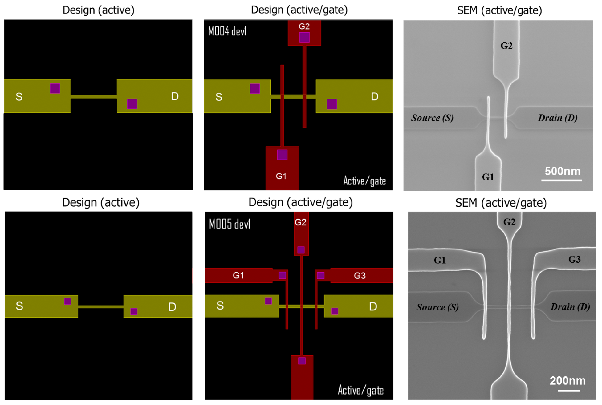
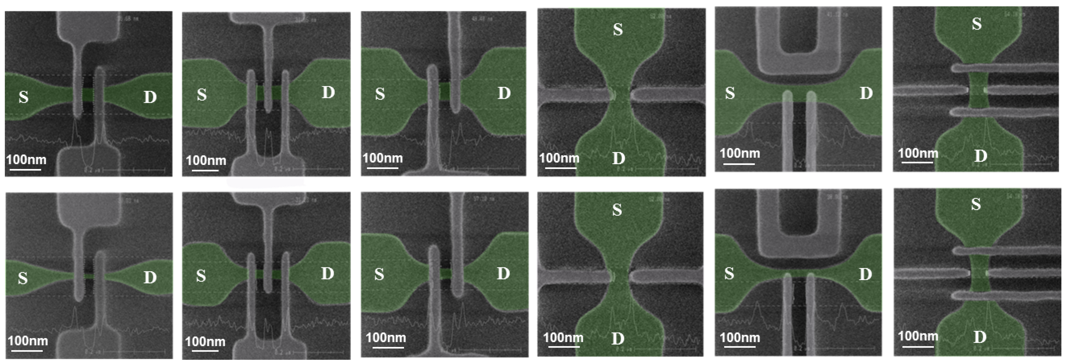
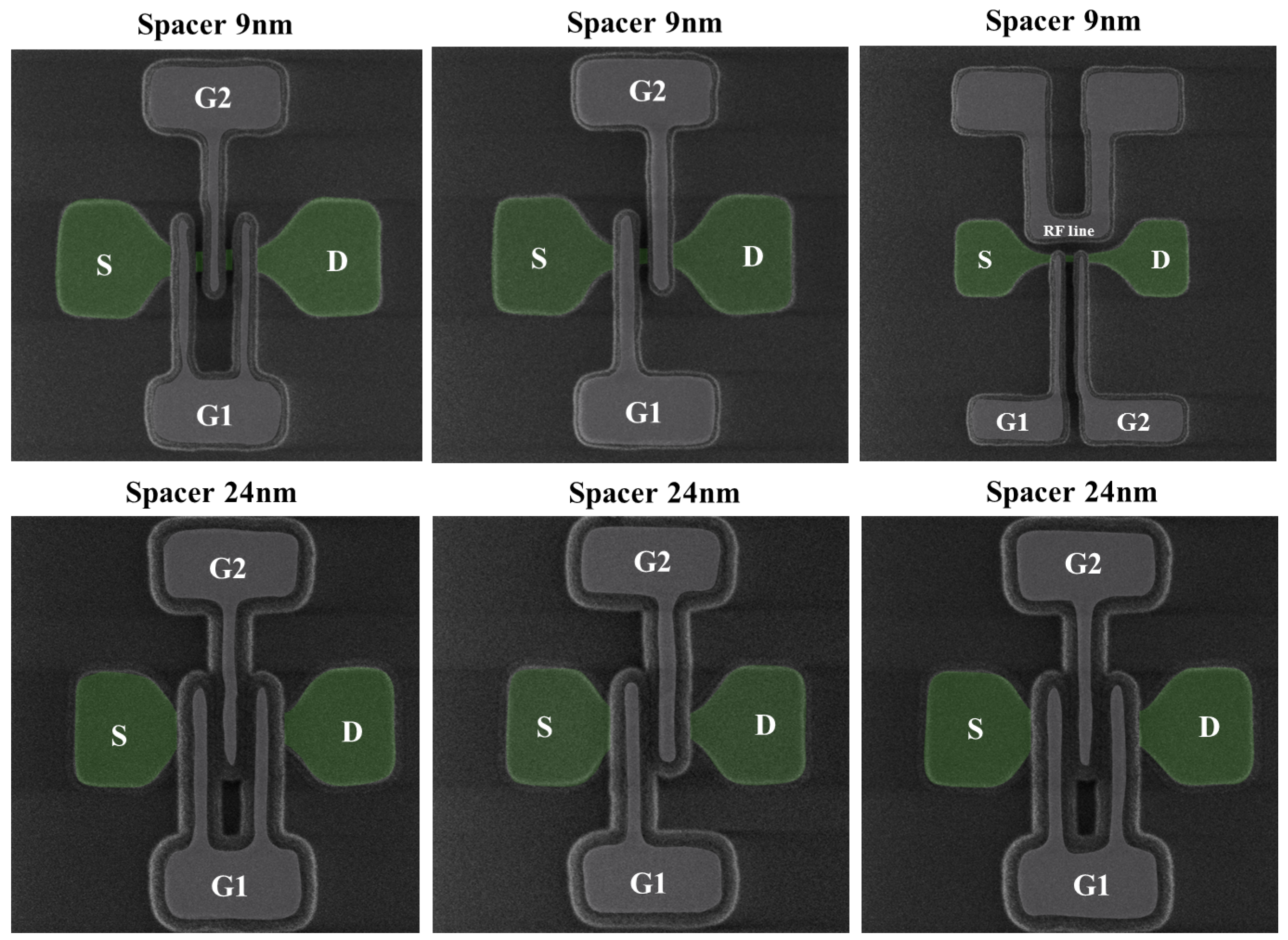
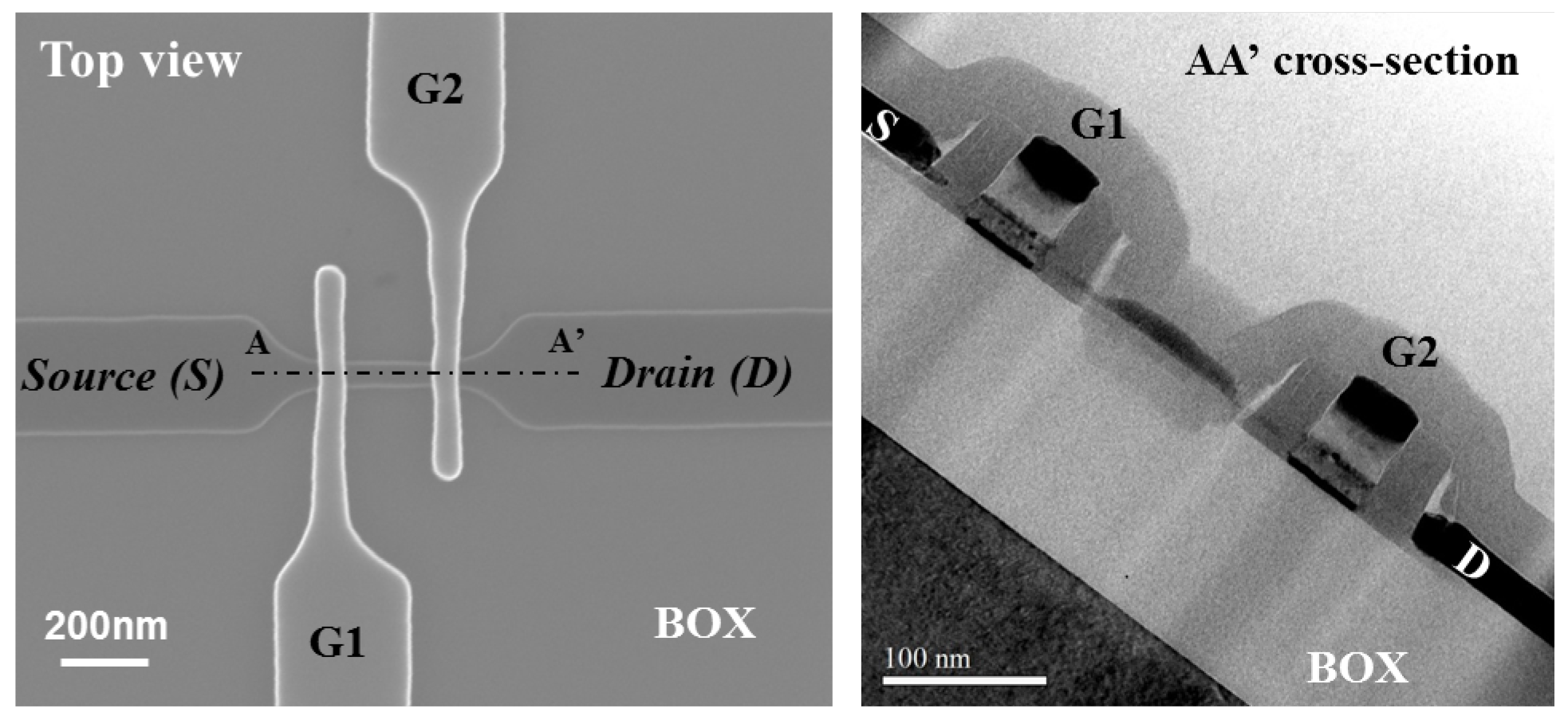
3.1. Active Area Patterning

[110]-oriented Nanowire (NW) field-effect-transistors (N- and P-MOS) with high-k/metal gate stack were fabricated on (100) SOI wafers with BOX (buried oxide) thickness of 145 nm. The silicon film thickness is approximately 13 nm. The silicon layer is patterned to create NWs by the mesa isolation technique, i.e., each transistor is isolated from each other with the SiO 2 buried oxide of the SOI substrate. NW patterns are defined by deep-UV (193nm) optical lithography and followed by a resist trimming process in order to shrink the dimensions of nanowires. Nanowire width down to 10 nm can be achieved after active patterning [9]. In Figure 2, Figure 3 and Figure 4, we show the active area of various structures, highlighted in green. Undoped or channel doping can be used.

3.2. Gate Patterning with a 65 nm Pitch

After the active area patterning a high-k/metal gate is deposited. The gate stack consists in a SiO 2 oxide of 2.5 nm, 2 nm CVD HfO 2 (high-k dielectric), 5 nm TiN (metal gate) made by atomic layer deposition and Poly-Silicon (50 nm) layers. The gate is wrapped around the channel like an omega-gate configuration. As for the active patterning, the same photo-resist trimming is used to achieve gate lengths down to 20 nm. Note that the 2.5 nm of SiO 2 is markedly larger than the usual value used for microelectronics applications, because we infer a large impact of remote Coulomb scattering in the gate stack. Hence pushing this interface further away could be an important point for low temperature applications. The benefits of e-beam gates is illustrated in Figure 2 and Figure 3. First, for two gates in series the spacing can be as low as 35 nm, compared to 170 nm in Figure 5. Another advantage is the relatively straightforward integration of more complex designs such as 3 or 4-gate pumps or pumps with an RF antenna in the vicinity of the island. Note however that a nearby detector based on another active area was not implemented in this study. This would require advanced patterning for the active area layer [10] which is possible in principle but has not been used in this work.
Afterwards a nitride spacer is formed on the sidewalls of the gate. Spacers are self-aligned since they consist of a nitride layer anisotropicaly etched, thus remaining only where a significant step height is present, i.e., at this stage all around the nearly 60 nm high gate stack. Spacer of thicknesses 9, 15 or 30 nm have been implemented (Figure 6). The thinner spacer allows creating a silicide area between the two gates in series, similar to the devices of “type C” in [11]. Then, low access resistances are realized by epitaxial silicon growth on the source and drain (T S i =18 nm). A second offset spacer consisting of a tetraethyl orthosilicate (TEOS) liner and a nitride layer was fabricated prior to source/drain implantations, activation spike anneal and silicidation (NiPtSi silicide), in order to obtain low contact resistances.
Finally, tungsten contact and standard Cu back-end-of-the-line process flows were used, as illustrated in Figure 7. As a result and in contrast with all other electron pumps reported so far, the devices are encapsulated with an industrial process. This could become important when exchanging and comparing samples between NMIs becomes a reality. It also ensures straightforward compatibility with circuit design tools, in order to build more complex circuits on-chip with electron pumps [12].

4. Electrical Characterizations at 300 K

The simple design of electron pumps relying on two NW FETs in series allows testing at 300 K, as illustrated in Figure 8. For this measurement a very small source-drain bias is applied (here 50 μV), in order to not saturate the high-gain (V/I of the order of 2 × 10 8 ) transimpedance amplifier used for subsequent measurements at low temperature. The maximum current measured (10 nA) thus corresponds to a resistance of 5 kΩ. The device shown on the left has a width of 50 nm and two gates of length 50 nm. For each backgate voltage a set of three curves is shown to illustrate the behaviour of each gate independently (green and blue curves, obtained by fixing one gate at +0.8 V while sweeping the other one) and the global behaviour ( V g 1 = V g 2 , red curves). A reasonable electrostatic control is obtained despite the two-gate layout which is not optimal: a slope of 90 mV/decade is obtained in the sub-threshold region. Moreover the backgate has a strong effect on the curves, allowing to tune the access resistances to the central island [13]. This additional knob offered by SOI technology is important for operation at low temperature, in particular to get away from impurities like donor states which induce a perturbation on the current maps [5]. On the right of Figure 8 we show the characteristics of a device with thinner silicon layer (T Si = 11 nm), narrower nanowire (W = 15 nm), 40 nm long gates and 30 nm spacing between them. It results in a nearly optimal slope of 68 mV/decade. The devices developped with our approach are now under systematic measurements to assess their metrological capabilities, in collaboration with NMIs. It is important to emphasize that the aggressive pitch (65 nm) we reached with our electron beam lithography gate level is now accessible with the most advanced industrial process [14] (14 nm node).

5. Conclusions

There is a need for robust and practical electron pumps to be shared and compared by NMIs for the quantum metrology of the forthcoming new ampere. In contrast with all other pumps realized in academic or small-scale fabrication facilities, we use a nearly industrial process to design and fabricate electron pumps and circuits. In this article we gave an overview of the most relevant process steps, including the custom gate level defined by electron beam lithography instead of the standard deep UV optical process used in production. This allows for a more aggressive pitch, of the order of 65 nm. We have shown a very good electrostatic control of the devices even for two-gate layouts which are the building blocks of electron pumps.

Acknowledgments

This work is partially supported by the EU through the FP7 ICT collaborative project SiAM (Project No. 610637). We also acknowledge support from the Fondation Nanosciences in Grenoble, through the Ph.D. and excellence chair programs.

Author Contributions

Sylvain Barraud, Romain Lavieville, Louis Hutin, Heorhii Bohuslavskyi and Maud Vinet designed and fabricated the devices, measured by Andrea Corna, Paul Clapera, Xavier Jehl and Marc Sanquer. All the authors participated in writing the manuscript.

Conflicts of Interest

The authors declare no conflict of interest.

References

  1. Blumenthal, M.D.; Kaestner, B.; Li, L.; Giblin, S.; Janssen, T.J.B.M.; Pepper, M.; Anderson, D.; Jones, G.; Ritchie, D.A. Gigahertz quantized charge pumping. Nat. Phys. 2007, 3, 343–347. [Google Scholar] [CrossRef]
  2. Giblin, S.; Kataoka, M.; Fletcher, J.; See, P.; Janssen, T.; Griffiths, J.; Jones, G.; Farrer, I.; Ritchie, D. Towards a quantum representation of the ampere using single electron pumps. Nat. Commun. 2012, 3, 930. [Google Scholar]
  3. Fricke, L.; Wulf, M.; Kaestner, B.; Hohls, F.; Mirovsky, P.; Mackrodt, B.; Dolata, R.; Weimann, T.; Pierz, K.; Siegner, U.; et al. Self-Referenced Single-Electron Quantized Current Source. Phys. Rev. Lett. 2014, 112, 226803. [Google Scholar]
  4. Kaestner, B.; Kashcheyevs, V. Non-adiabatic quantized charge pumping with tunable-barrier quantum dots: A review of current progress. Rep. Prog. Phys. 2015, 78, 103901. [Google Scholar] [CrossRef] [PubMed]
  5. Jehl, X.; Voisin, B.; Charron, T.; Clapera, P.; Ray, S.; Roche, B.; Sanquer, M.; Djordjevic, S.; Devoille, L.; Wacquez, R.; et al. Hybrid Metal-Semiconductor Electron Pump for Quantum Metrology. Phys. Rev. X 2013, 3, 021012. [Google Scholar] [CrossRef]
  6. Clapera, P. Design and operation of CMOS-compatible electron pumps fabricated with optical lithography. IEEE Electron Device Lett. 2016. submitted. [Google Scholar]
  7. Rossi, A.; Tanttu, T.; Tan, K.Y.; Iisakka, I.; Zhao, R.; Chan, K.W.; Tettamanzi, G.C.; Rogge, S.; Dzurak, A.S.; et al. An Accurate Single-Electron Pump Based on a Highly Tunable Silicon Quantum Dot. Nano Lett. 2014, 14, 3405–3411. [Google Scholar] [CrossRef] [PubMed]
  8. Yamahata, G.; Karasawa, T.; Fujiwara, A. Gigahertz single-hole transfer in Si tunable-barrier pumps. Appl. Phys. Lett. 2015, 106, 023112. [Google Scholar] [CrossRef]
  9. Barraud, S.; Coquand, R.; Casse, M.; Koyama, M.; Hartmann, J.; Maffini-Alvaro, V.; Comboroure, C.; Vizioz, C.; Aussenac, F.; Faynot, O.; et al. Performance of Omega-Shaped-Gate Silicon Nanowire MOSFET With Diameter Down to 8 nm. IEEE Electron. Device Lett. 2012, 33, 1526–1528. [Google Scholar] [CrossRef]
  10. Gaben, L.; Barraud, S.; Pimenta-Barros, P.; Morand, Y.; Pradelles, J.; Samson, M.P.; Previtali, B.; Besson, P.; Allain, F.; Monfray, S.; et al. Omega-Gate Nanowire Transistors Realized by Sidewall Image Transfer Patterning: 35 nm channel pitch and opportunities for stacked-Nanowires architectures. In Proceedings of the International Conference on Solid-State Devices and Materials, Sapporo, Japan, 27–30 September 2015.
  11. Pierre, M.; Roche, B.; Wacquez, R.; Jehl, X.; Sanquer, M.; Vinet, M. Intrinsic and doped coupled quantum dots created by local modulation of implantation in a silicon nanowire. J. Appl. Phys. 2011, 109, 084346. [Google Scholar] [CrossRef]
  12. Clapera, P.; Ray, S.; Jehl, X.; Sanquer, M.; Valentian, A.; Barraud, S. Design and Cryogenic Operation of a Hybrid Quantum-CMOS Circuit. Phys. Rev. Appl. 2015, 4, 044009. [Google Scholar] [CrossRef]
  13. Roche, B.; Voisin, B.; Jehl, X.; Wacquez, R.; Sanquer, M.; Vinet, M.; Deshpande, V.; Previtali, B. A tunable, dual mode field-effect or single electron transistor. Appl. Phys. Lett. 2012, 100, 032107. [Google Scholar] [CrossRef]
  14. Natarajan, S.; Agostinelli, M.; Akbar, S.; Bost, M.; Bowonder, A.; Chikarmane, V.; Chouksey, S.; Dasgupta, A.; Fischer, K.; Fu, Q.; et al. A 14 nm logic technology featuring 2nd-generation FinFET, air-gapped interconnects, self-aligned double patterning and a 0.0588 μm2 SRAM cell size. In Proceedings of the IEEE International Electron Devices Meeting (IEDM), San Francisco, CA, USA, 15–17 December 2014.
Figure 1. Two-gate and three-gate devices realized with deep-UV lithography. Left: mask design with the nanowire (yellow) and its Source (S) and Drain (D) extremities, and the two and three gates in red; Right: Scanning electron micrograph of actual devices, with a gate pitch of 190 nm.
Technologies 04 00010 g001
Figure 2. Examples of samples after gate patterning. Active (resp. gate) area is represented in green (grey) color. Multi-gate devices are realized with a 65 nm gate pitch.
Technologies 04 00010 g002
Figure 3. Examples of two-gate devices after gate patterning for narrow (15 nm) and wide (40 nm) nanowire width. Active (resp. gate) area is represented in green (grey) color. Top: Scanning electron micrograph of two-gate device. The two gates partially overlap the active area and a RF line is located in the vicinity of the Si islands; Bottom: Scanning electron micrograph of two-gate device used for electron pumps. The minimal spacing between gates is 30 nm.
Technologies 04 00010 g003
Figure 4. Examples of samples after spacer patterning. Multi-gate devices are realized with a 65 nm gate pitch. Active (resp. gate) area is represented in green (grey) color. Top: a thin spacer (9 nm) is used in order to create a silicide area between the two gates; Bottom: a thick spacer (24 nm) is used in order to avoid salicidation between the two gates.
Technologies 04 00010 g004
Figure 5. Two-gate device realized with deep-UV lithography. Left: Scanning electron micrograph of an actual device, with a gate pitch of 190 nm; Right: Transmission electron micrograph of two-gate device realized with wide spacer (40 nm).
Technologies 04 00010 g005
Figure 6. Examples of samples after Si source-drain epitaxy. Multi-gate devices are realized with a 65 nm gate pitch. Top: a thin spacer (9 nm) is used in order to create a silicide area between the two gates; Bottom: a thick spacer (24 nm) is used in order to avoid salicidation between the two gates.
Technologies 04 00010 g006
Figure 7. Transmission electron micrograph of single-gate device after back-end process. The device is at the center, and only the Source and Drain vertical vias and copper lines are visible. Tungsten contact and standard Cu back-end-of-the-line process are used, as usual for advanced CMOS transistors.
Technologies 04 00010 g007
Figure 8. Left: Drain-Source current versus gate voltages at 300 K and at three values of the backgate voltage in a two-gate electron pump. For the red curves the two gates are swept together. For the blue and green curves one gate is swept while the other one is kept at +0.8 V. The sub-threshold slope measured here is ≈ 90 mV/decade. The degradation compared to the ideal value of 60 mV/decade at 300 K is mostly due to the thick silicon layer (T Si = 20 nm); Right: Same data (except for the two gates at the same voltage, not shown) at zero backgate voltage in a device with very good electrostatic control (slope of 68 mV/decade) thanks to a much thinner silicon layer (T Si = 11 nm). The black dashed line shows the ideal slope of 60 mV/decade.
Technologies 04 00010 g008

