Piezoelectric Thick Film Deposition via Powder/Granule Spray in Vacuum: A Review
by

Deepak Rajaram Patil
1, 
Venkateswarlu Annapureddy
2,
J. Kaarthik
2,
Atul Thakre
1,
Jun Akedo
3 and
Jungho Ryu
1,4,* 1
School of Materials Science and Engineering, Yeungnam University, Gyeongsan 38541, Korea
2
Department of Physics, National Institute of Technology Tiruchirappalli, Tiruchirappalli, Tamil Nadu 620015, India
3
National Institute of Advanced Industrial Science and Technology (AIST), Tsukuba 305-8560, Japan
4
Institute of Materials Technology, School of Materials Science and Engineering, Yeungnam University, Gyeongsan 38541, Korea
*
Author to whom correspondence should be addressed.
Actuators 2020, 9(3), 59; https://0-doi-org.brum.beds.ac.uk/10.3390/act9030059
Submission received: 10 June 2020
/
Revised: 3 July 2020
/
Accepted: 3 July 2020
/
Published: 23 July 2020
(This article belongs to the Special Issue Piezoelectric Actuators and Ultrasonic Motors: Future Perspectives)
Abstract
:Conventional thin-film processing techniques remain inadequate for obtaining superior dense ceramic thick films. The incompatibility of ceramic films prepared via other methods, such as screen printing, spin coating, and sputtering, is a major obstacle in the fabrication of thick film-based ceramic electronic components. The granule spray in vacuum (GSV) processes and aerosol deposition (AD) are important coating approaches for forming dense ceramic thick films featuring nanoscale crystallite structures at room temperature, which offer excellent material properties and facilitate cost-effective production. AD ceramic coatings require the acceleration of solid-state submicron ceramic particles via gas streams with a velocity of a few hundred meters per second, which are then wedged onto a substrate. This process is economical and particularly useful for the fabrication of piezoelectric thick film-based microactuators, energy harvesters, sensors, and optoelectronic devices. More recently, the GSV technique was improved to achieve more uniform and homogeneous film deposition after AD. This review article presents a detailed overview of the AD and GSV processes for piezoelectric thick films in terms of recent scientific and technological applications.
1. Introduction
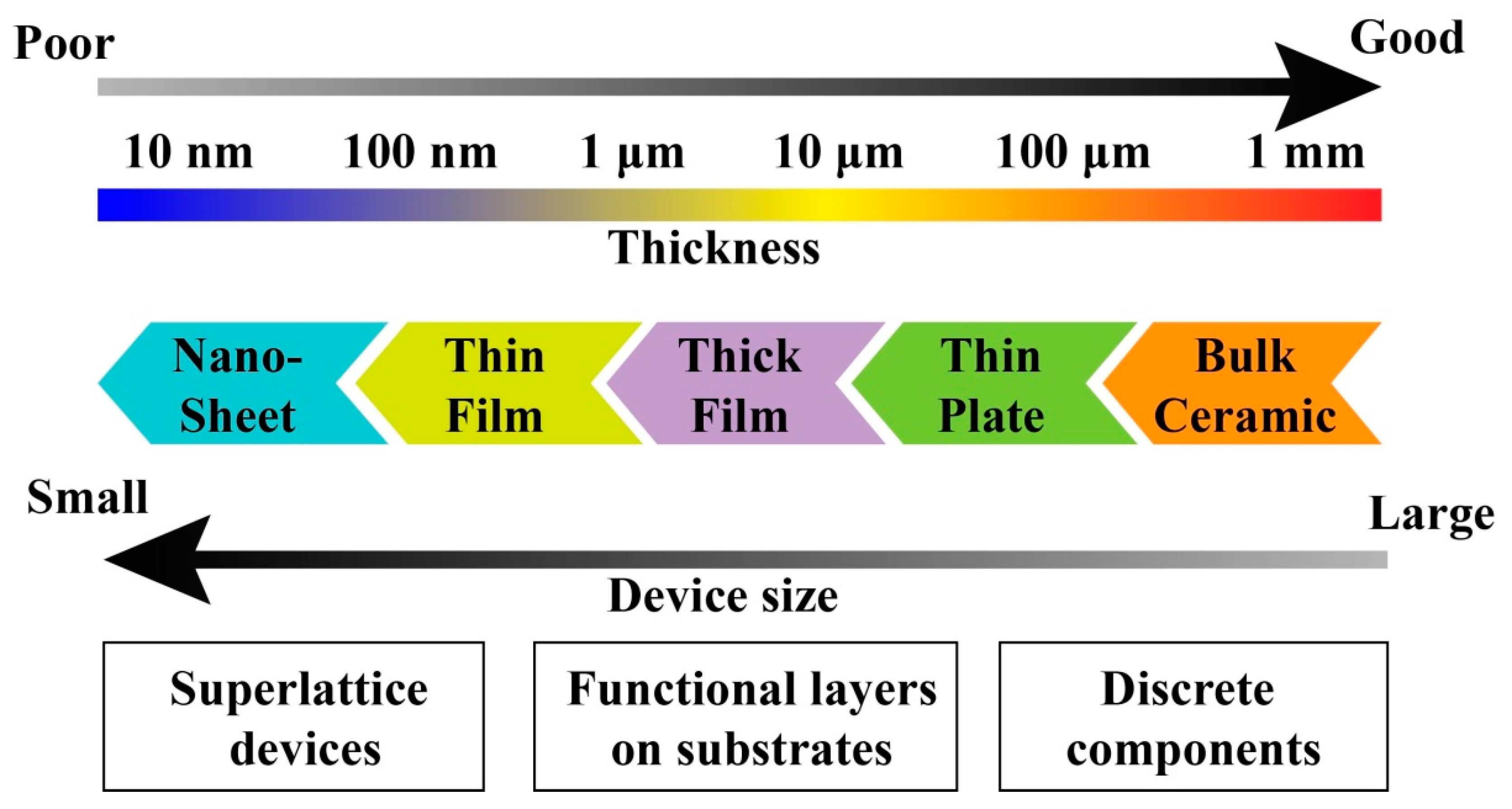
The synthesis of dense ceramic involves high-temperature firing (≥1000 °C). As structures encompassing substrates, such as glass, metal, or plastic, are more delicate under such high temperatures, assimilating them into a useful device structure is challenging. Moreover, the high-temperature annealing or sintering of ceramic components results in uncontrolled volatilization or decomposition. This necessitates the development of ground-breaking engineering processes for fabricating high-performance functional devices with dense films, which consequently reduces the cost of device fabrication. Figure 1 depicts the scope of piezoelectric films with different thickness values for various applications. Films with a thickness of 1–100 µm are primarily employed for the successful fabrication of microelectromechanical systems (MEMS), actuators, etc. [1]. Therefore, there is a need to develop a novel method for processing thick films to ensure integration competence in circuits and/or miniaturized devices.
Film thickness plays a vital role in the construction of application-oriented devices, and also influences the working efficiency of thick films. For instance, in piezoelectric actuator applications, the performance of a device is based on film thickness; a very thin piezoelectric film may generate a significantly small displacement/force. Conversely, very thick films may require excessive driving voltages. Therefore, several μm-thick films are essential for applications such as actuators to efficiently convert the input electrical energy to the output mechanical energy. When a thick film of several μm is formed onto a substrate by means of conventional technologies, such as sol–gel or sputtering methods, various problems might occur, including a slow deposition rate or variable composition. Owing to these concerns, conventional thin film deposition technologies have been generally used to merely fabricate thin films with limited thicknesses of approximately ≤1 µm. Thus, it can be concluded that the fabrication of piezoelectric thick films via conventional methods is practically challenging [1].
The screen-printing method that utilizes a mixture of ceramic powder and binder is one of the approaches for the production of thick films. However, this strategy has been developed based on conventional technology, which requires the sintering of ceramic materials, wherein the material is heated to a high temperature of ≥1000 °C. Moreover, the choice of the substrate material is typically limited to only ceramics in this technique. It is evident that conventional methods suffer from several disadvantages, such as high processing temperatures and limitations over the thickness for fine patterning. Recently, several methods have been developed with the aim of reducing the sintering temperature, considering the large energy consumption, and integrating innovative functional components with low melting temperature substrates, such as glass, metal, or flexible polymers. Recently, the cold spray method for fabricating thick films on the metal substrate has attracted considerable attention. In this method, micron-sized particle jets are accelerated and transported to the substrates at high speeds. Upon impacting the substrates, the solid particles adhere to the surface of the substrate and form coatings with high density and less porosity. However, this method is unsuitable for depositing ceramic thick films.
A promising alternative to these conventional ceramics methods is aerosol deposition (AD), which employs the impact consolidation of fine ceramic powders to form a dense ceramic coating at room temperature (RT) [2]. It is possible to fabricate thick films exceeding 100 μm through this process. Moreover, the AD process occurs at RT; hence, the high-temperature firing of ceramic films is avoided. Therefore, AD serves as one of the simplest methods, without requiring any complex processes. AD is also referred to as vacuum kinetic spraying or vacuum cold spraying, as well as “powder aerosol deposition” to differ from liquid aerosol technology [3].
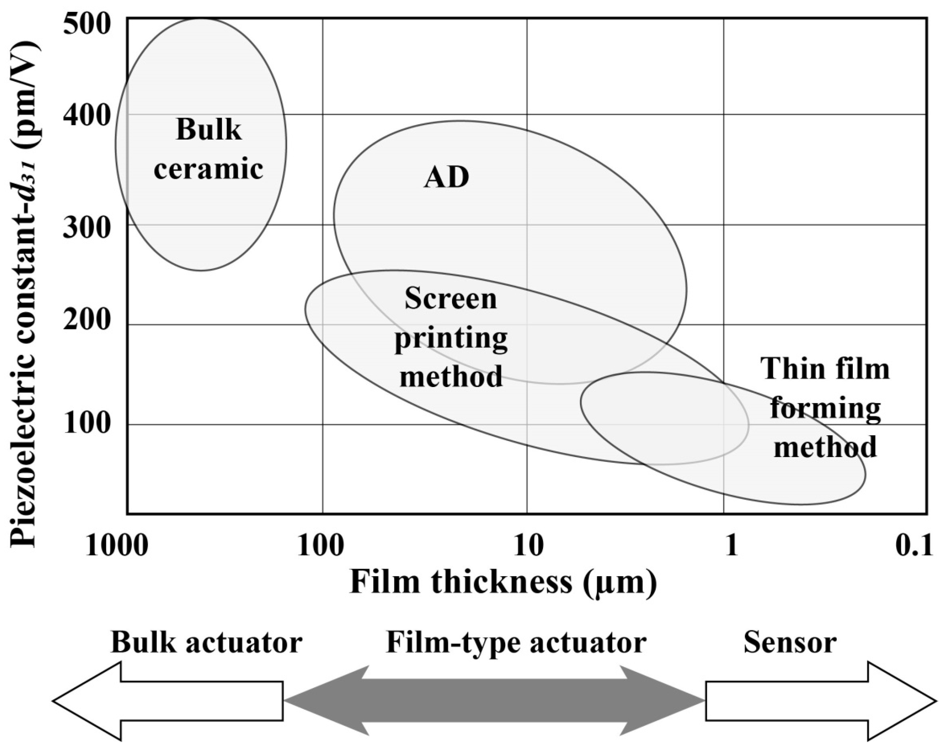
Figure 2 presents a comparison of the piezoelectric properties of thin/thick films formed via AD and other conventional film deposition methods. The AD film deposited on the stainless steel substrate exhibited a piezoelectric constant (−d31) of 158 pm/V, which is approximately equal to that of films fabricated using conventional thin film deposition technologies [4]. On a Zirconate substrate, a −d31 of 360 pm/V was achieved, which was comparable to that of bulk ceramics [5]. In AD, dense and thick ceramic coatings are formed at room temperature by aerosolizing ceramic microparticles with diameters ranging from several hundred nm to several µm in the gas fluid; the particles remain in the solid-state form without any binder composition and are sprayed onto a substrate material under reduced pressure. AD enables the production of high-density polycrystalline films from bulk powder without requiring any high-temperature process for any type of substrate material.
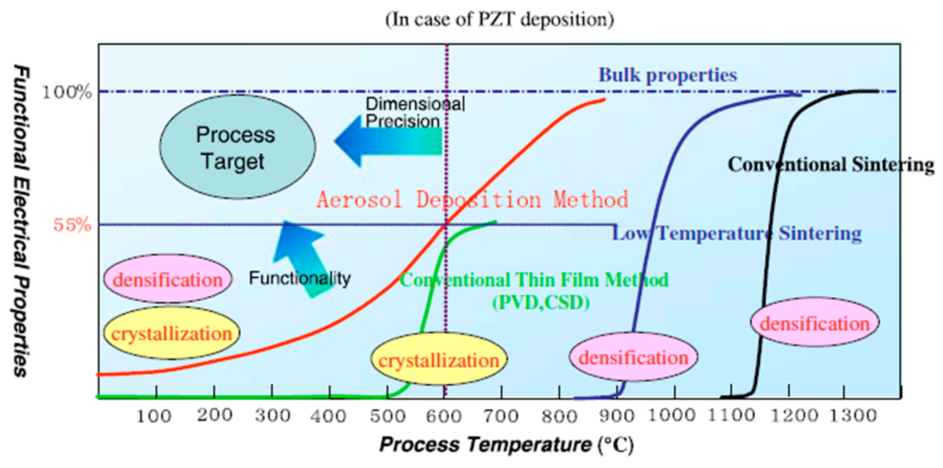
Figure 3 summarizes the annealing temperature-dependent ferroelectric properties of lead zirconate titanate (PZT) films prepared via AD, as compared to the conventional process. The films fabricated through conventional processes required heat treatments exceeding 600 °C for their crystallization and densification. On the other hand, AD enables a 300–400 °C reduction of the post-process temperature, even without the addition of any special additives to the feed particles. Most importantly, the as-deposited films by AD have a denser and more crystallized structure because they are near the bulk material [2], even before sintering. Consequently, piezoelectric and ferroelectric properties are further improved via additional annealing of the films. Furthermore, there is no shrinkage of the AD layer before and after annealing. Therefore, AD layers are referred to as “high-density ceramic green without binders” [2]. Using this method, various ceramics, such as BaTiO3 [6], BaSrTiO3 [7], (K,Na)NbO3 [8], Pb(Zr,Ti)O3 [5], α-Al2O3 [9], and MgB2 [10] were deposited as thick films at RT with enhanced physical properties such as a high breakdown voltage.
2. Room-Temperature Aerosol Deposition
2.1. Construction of AD System
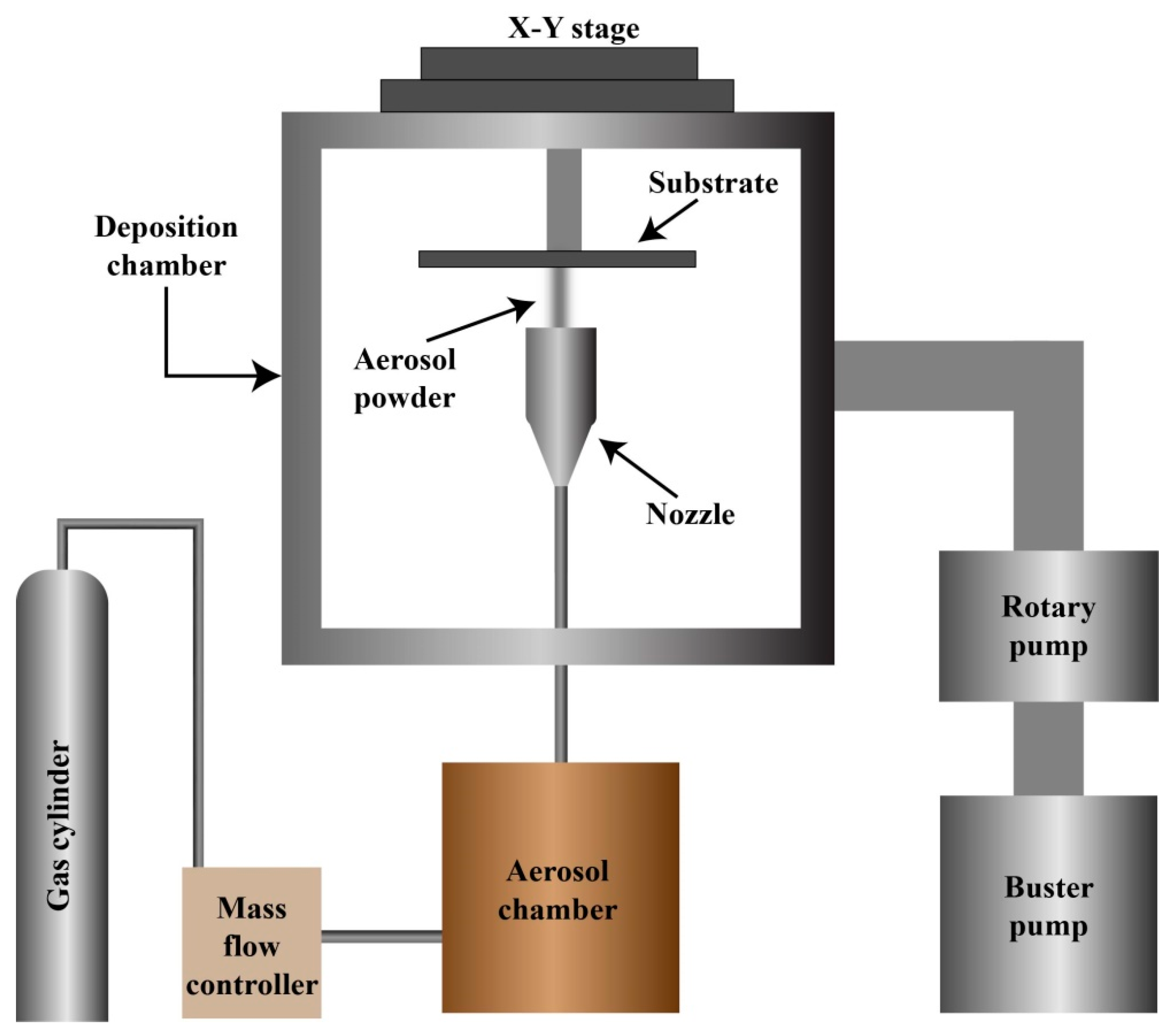
Figure 4 depicts the setup of the AD system, and the appropriate deposition conditions for the AD process are listed in Table 1. The setup comprises the following components: (a) two vacuum chambers, i.e., a deposition chamber where film deposition occurs and the aerosol chamber where ceramic powders get aerosolized for deposition; and (b) a vacuum pump (rotary type with a mechanical booster) to generate a vacuum for facilitating the deposition. A carrier gas, such as dried air, O2, Ne, and He, [9] is passed into the aerosol chamber, wherein an aerosol is formed by mixing the carrier gas with fine-sized powders within the vicinity of a micron. A conventional AD setup [11,12], wherein large-area films are deposited on a flat plate by means of a nozzle using the movable x–y axes stage, is used to deposit thick ceramic films. A mass flow controller was used to regulate particle velocities through mass flow consumption [13]. A vacuum pump is used to generate a constant pressure difference in the aerosol, deposition chamber, and aerosol chamber, which helps transport the generated aerosol to the deposition chamber. The generated aerosol is then accelerated with a velocity of a few hundred meters per second via a nozzle. Upon entering the deposition chamber, the accelerated particles collide with the substrate mounted on the x–y stage and form a firmly adhering ceramic film. Occasionally, filters and classificators are used between the aerosol-generation and deposition chambers to generate a jet of particles with acceptable sizes and morphologies. For large-sized particles and agglomeration, the filters and classificators break the particles apart as much as possible in order to obtain particles within a prescribed size range.
2.2. Working Principle
During deposition, the aerosol formed by the suspension of ceramic powders (particle size of approximately 0.08–2.0 μm) in a carrier gas is accelerated to several hundreds of meters per second and directly impacts the desired substrate. During particle–substrate collision, the kinetic energy of the particles is converted to heat energy, which consequently increases the local surface temperature of the substrate within a few nanoseconds, resulting in strong bonding between the substrate and accelerated particles via fracture and plastic deformation. Thus, a dense and thick film is formed [14,15]. For successful deposition, particle size selection and distribution are essential parameters. A particle size analyzer helps to precisely measure particle diameters and distribution. The initial particle size and degree of aggregation of the particles play a significantly important role in the formation of thick films [13].
2.3. Limitations of AD
Two major obstacles need to be surmounted for successful AD: (i) maintaining aerosol density and (ii) controlling the initial agglomeration of particles. These difficulties can be overcome by utilizing a de-agglomeration device.
2.4. Granule Spray in Vacuum
Granule spray in vacuum (GSV) is an RT deposition method for dense nanostructured ceramic films through the stable feeding of powder granules that are flowable agglomerates of fine primary powder particles [2]. GSV is an improved version of AD, and it offers continuous and uniform particle feeding to the nozzle. In GSV, intentionally agglomerated granule powders, i.e., finely crushed powder agglomerates during deposition, are used as the starting material because of their more free-flowing nature in order to ensure that the agglomeration issues can be regulated. GSV, in turn, produces a higher kinetic energy under the same gas flow conditions; however, it requires higher speeds to produce a larger kinetic energy for breaking the granules.
3. Fabrication of Lead-Based Piezoelectric Ceramic Materials
3.1. Fabrication of PZT Thick Films
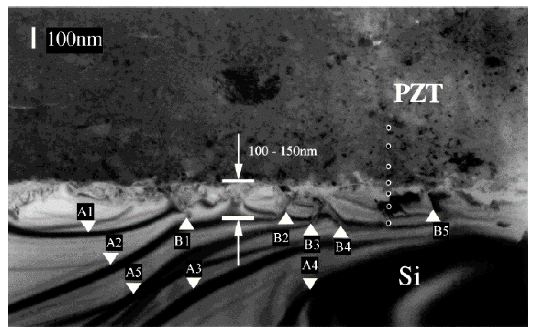
AD is widely used for the fabrication of PZT-based thick films with thicknesses exceeding 10 µm [11,16,17,18,19]. Akedo et al. deposited PZT films on Pt/Ti/SiO2/Si and Si substrates through AD [11]. Figure 5 presents the cross-sectional transmission electron microscopy (TEM) image of a 30-µm PZT thick film deposited using AD at RT. The density of the PZT layer was found to be 7.76 g/cm3, which represents 95% of its theoretical density. This indicates that the dense structure is formed by the fracturing of the starting particles during layer formation. A type of damage layer with a thickness of 100–150 nm was also observed at the PZT/Si substrate interface. The stacking faults (marked as B1–B5 in Figure 5) induced several deformations (marked as A1–A5 in Figure 5) inside the Si wafer due to mechanical shock compression. The hardness of the deposited layer is measured to be 530, which is less than that of the Si. The as-deposited films at RT consist of randomly oriented crystallites with sizes of 40 nm, which is considerably smaller than the primary powder grain sizes and the large crystallites with sizes of 100–300 nm.
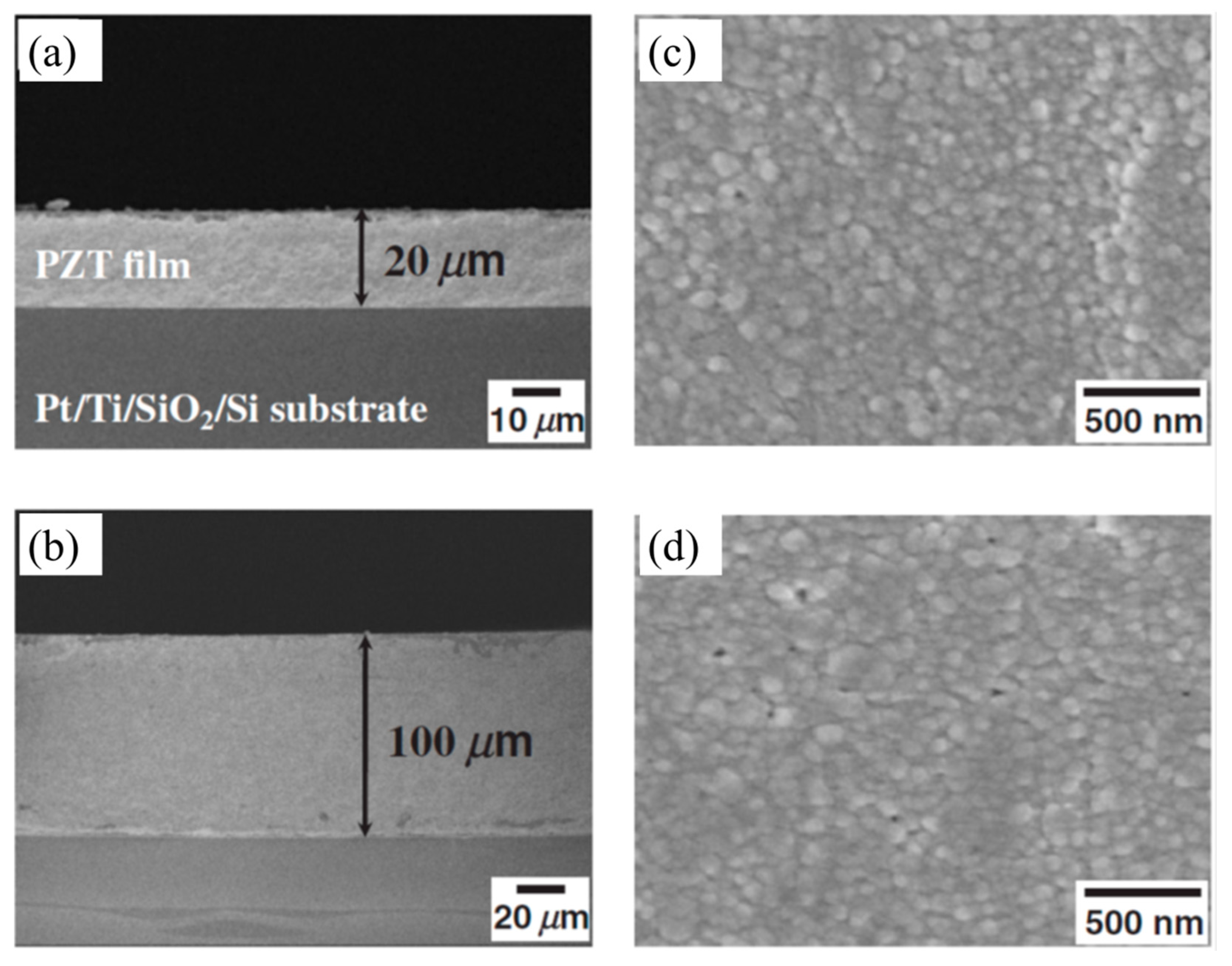
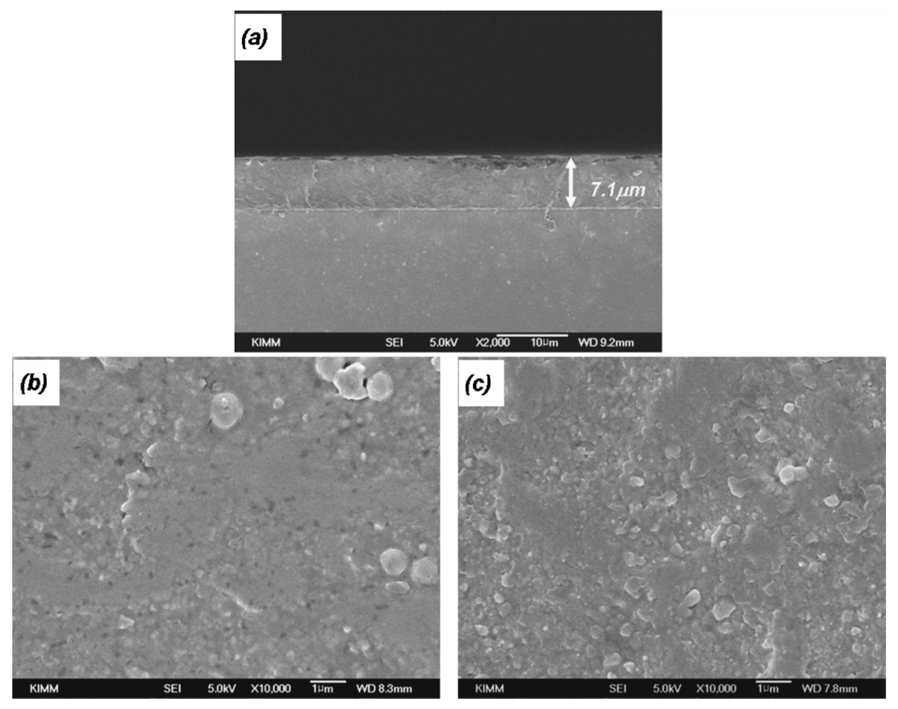
AD has paved the way for the successful deposition of thicker films with superior bonding quality; surprisingly, it also requires a processing temperature of RT. However, in AD, the films develop intrinsic compressive stress [20,21,22] upon the impact of ceramic microparticles onto the substrate and extrinsic thermal stress owing to the difference in the thermal expansion coefficients of the film and substrate. Several approaches have been investigated to eliminate these residual stresses in thicker films. For example, Hahn et al. introduced fine pores within the films to eliminate the intrinsic residual stress and fabricated crack-free PZT films with a thickness exceeding 20 µm [22]. Another approach is stress relaxation by using organic powders, such as polyvinylidene fluoride (PVDF) with AD-derived PZT films [23]. During the post-annealing of PZT films, the PVDF evaporates and results in stress relaxation, and PZT thick films of over 20 µm–100 µm were successfully obtained on the Si-based substrate via this approach, as shown in Figure 6.
3.2. Material Properties of AD Thick Films
3.2.1. Piezoelectric Properties
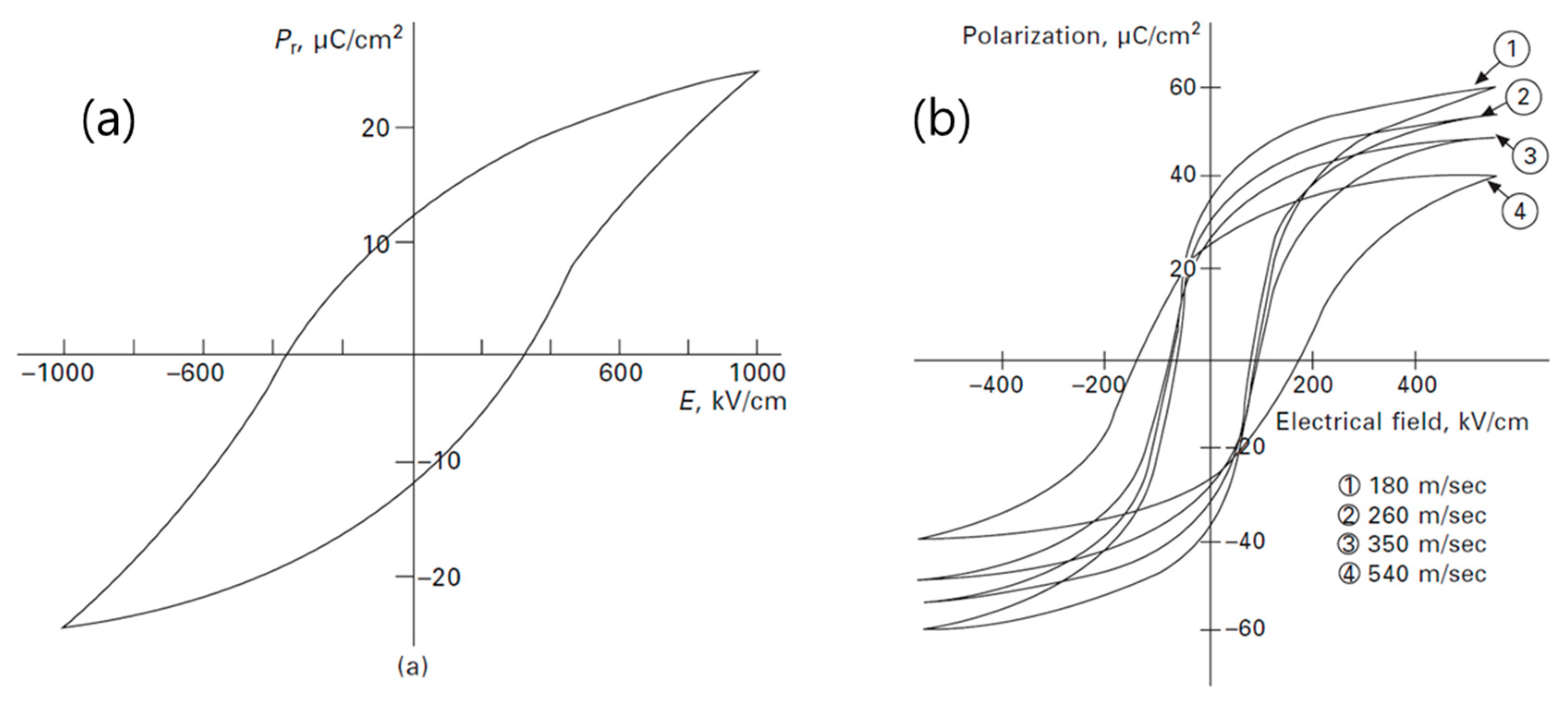
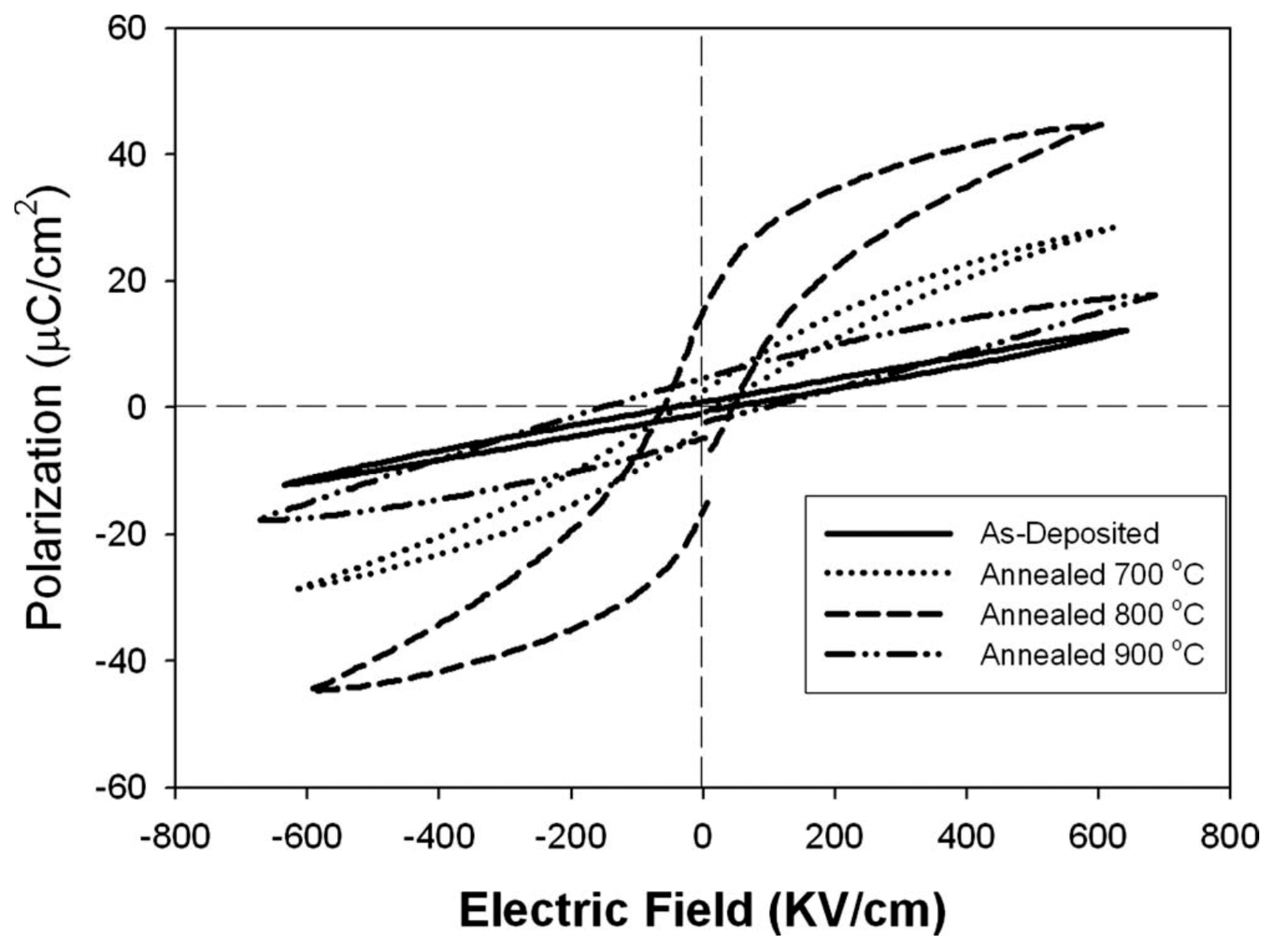
Although as-deposited AD PZT layers exhibit improved piezoelectric and ferroelectric behaviors, they are unsuitable for device applications due to their structural imperfections and crystallite size reduction. By conducting post-annealing of these as-deposited films from 500–600 °C, defect-free films are obtained along with adequate crystallite growth, which consequently enhances the ferroelectric properties of the film. d31 and the dielectric constant of the post-annealed films at 600 °C were −100 pm/V and 800–1200 [18], respectively, which were analogous to the values reported for conventional thin film methods. Moreover, the Young’s modulus (>80 GPa) and electrical breakdown (<1 MV/cm) for the AD films are higher than those achieved for conventional thick film technologies. A remnant polarization (Pr) of 38 μC/cm2 and coercive field strength (Ec) of 30 kV/cm were obtained for the post-annealed PZT films at 600 °C, [24,25] which is much higher than that of as deposited PZT film (Figure 7).
3.2.2. Stress-Related Influences in Thick Films
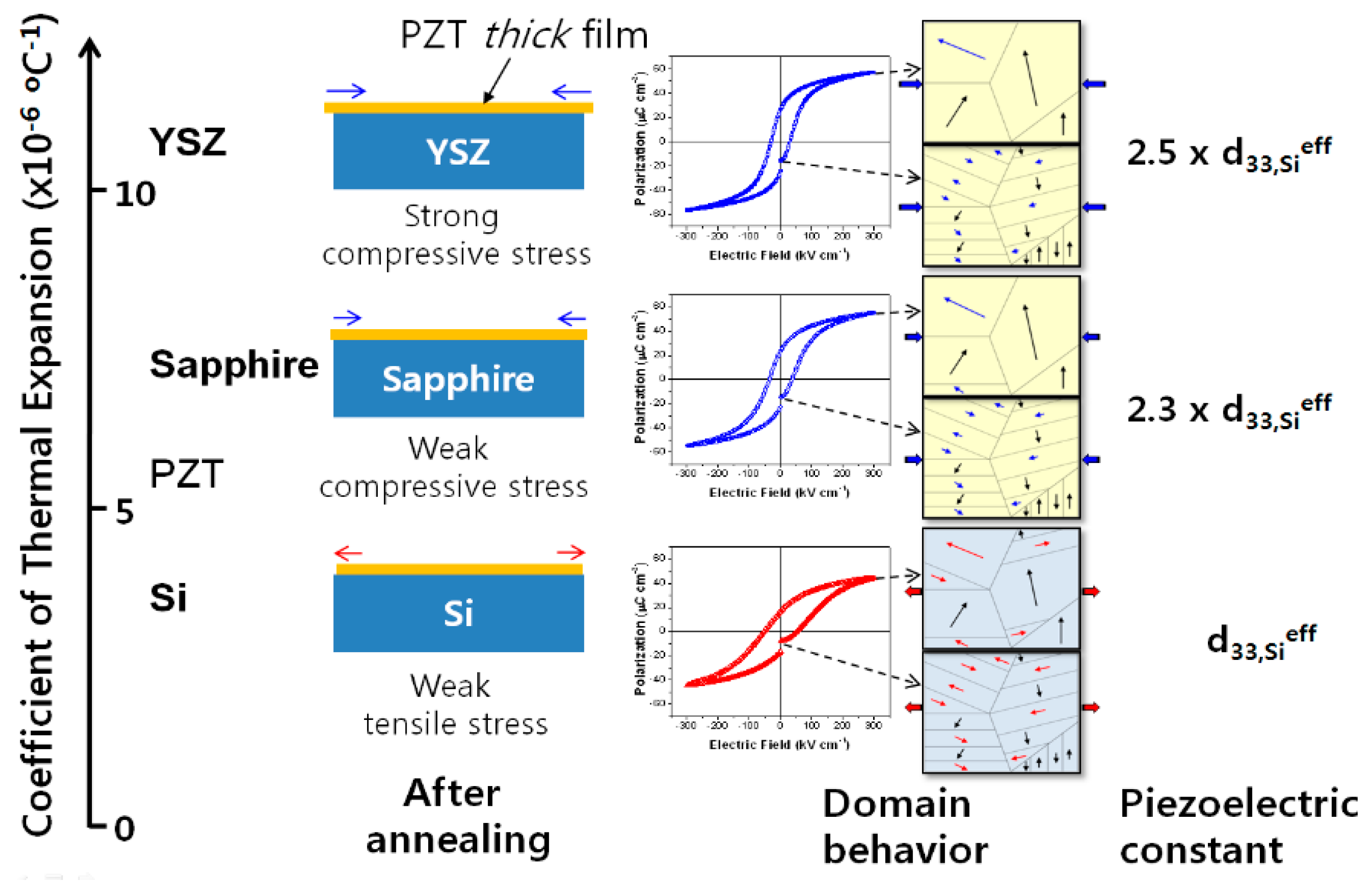
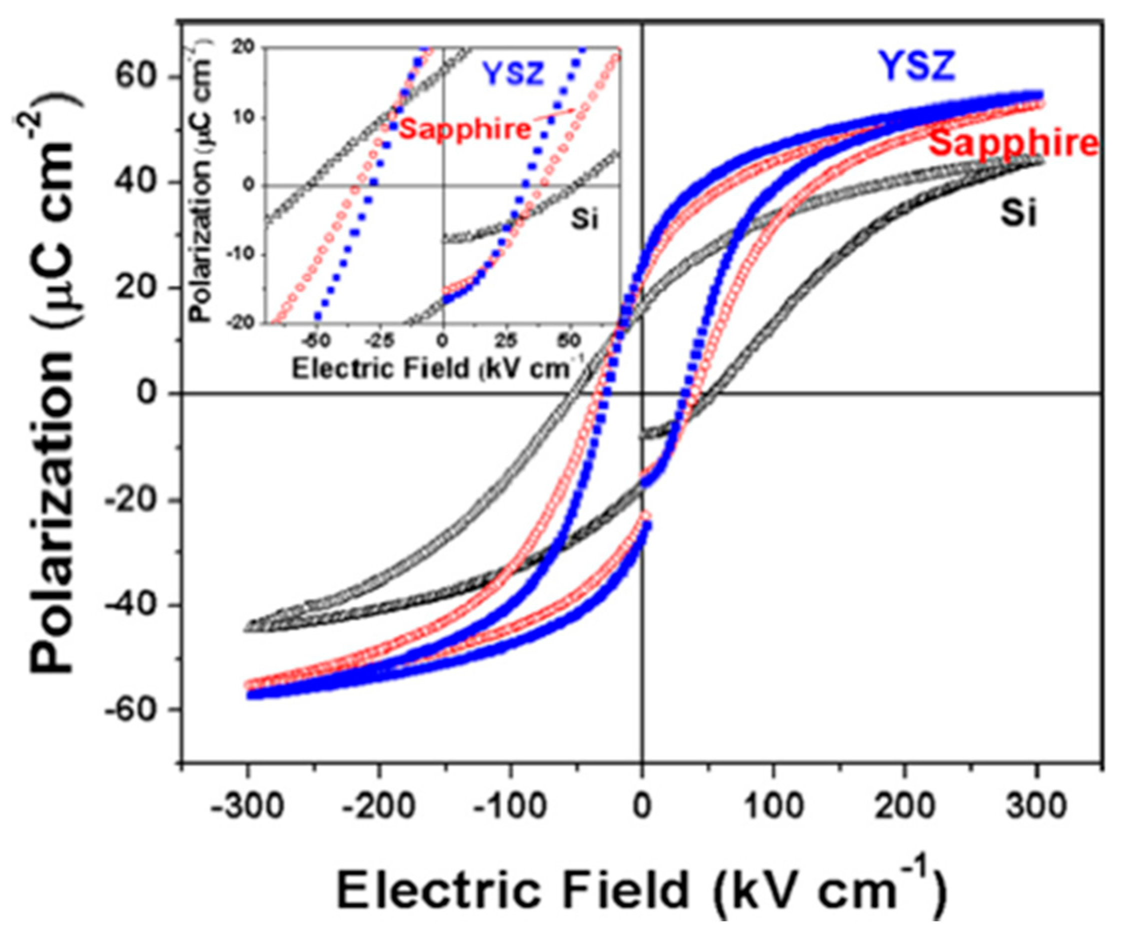
Han et al. [26] investigated the influence of the magnitude of compressive and tensile stresses on the domain alignment and crystal structure of thick films; they discovered that interfacial stress could be controlled by choosing substrates with a different coefficient of thermal expansion (CTE), such as Si, Sapphire (Al2O3), and yttria-stabilized zirconia (YSZ), as shown in Figure 8. They grew 10-μm-thick PZT films on each of these substrates and investigated their stress effects on the electronic properties of the film. The resultant polarization–electric field (P-E) loops are shown in Figure 8. It was found that the films on the Si substrate experience a weak tensile stress; consequently, they exhibit a mediocre ferroelectric response. However, the films on the YSZ and sapphire substrates exhibited significant enhancements in their ferroelectric and piezoelectric responses (Figure 8). These different responses occurred due to the differences in the CTE between the films and substrates. The films on the sapphire substrate exhibited a weaker compressive stress, whereas those on the YSZ substrates exhibited the highest compressive stress. The PZT films on the YSZ substrate evinced superior properties compared to those of the other PZT films on the two other substrates. Thus, this work recommends that the properties of a thick film can be controlled by simply choosing substrates with different CTEs.
Figure 9 presents the ferroelectric hysteresis loops of PZT films grown on different substrates. As apparent from the figure, the PZT film grown on the Si substrate exhibited the lowest saturation and remnant polarization but the highest coercive field. Conversely, the PZT films grown on the YSZ substrate exhibited the highest saturation and remnant polarization with the lowest coercive field.
3.3. Laser Annealing of AD Thick Films
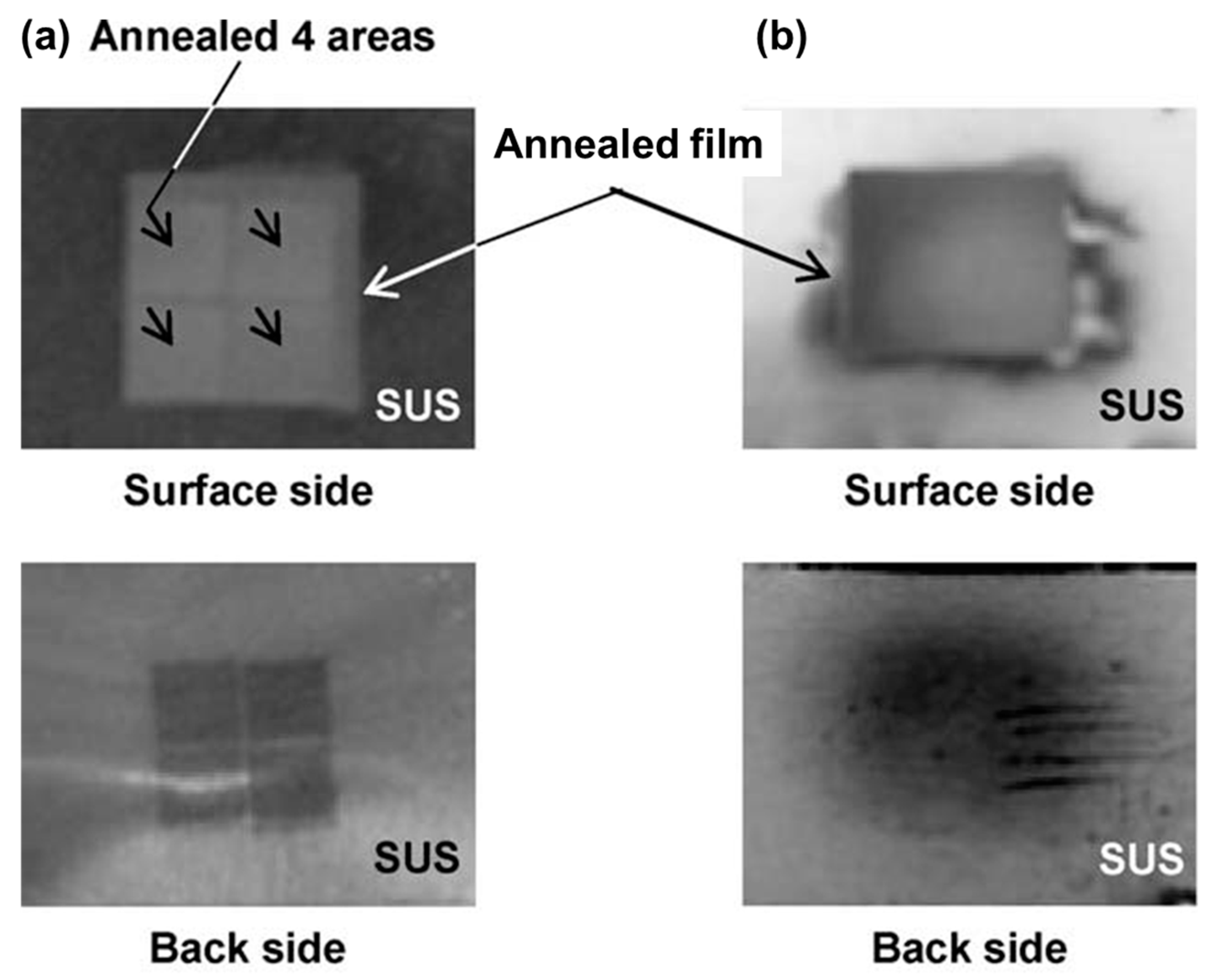
In AD-derived microstructures, temperature-sensitive substrate materials such as metals are typically involved. Conventional sintering techniques may damage the associated substrate. Thus, a special thermal method is required to treat thick films. Hence, laser annealing is suggested for the post-thermal process of PZT thick films over metal substrates, such as stainless steel, for MEMS devices. Baba et al. investigated this laser irradiation by using two sources—CO2 laser and fiber laser (FL)—for the deposition of PZT thick films over a stainless-steel substrate (PZT/STS). They found that the CO2 laser results in considerable thermal damage to the associated substrate, whereas FL irradiation suppresses thermal damage to the substrate. Compared to a CO2 laser, FL offers multiple advantages, including high vibrational stability and good beam quality [27]. Figure 10 presents photographs of the PZT films annealed using the CO2 laser and FS.
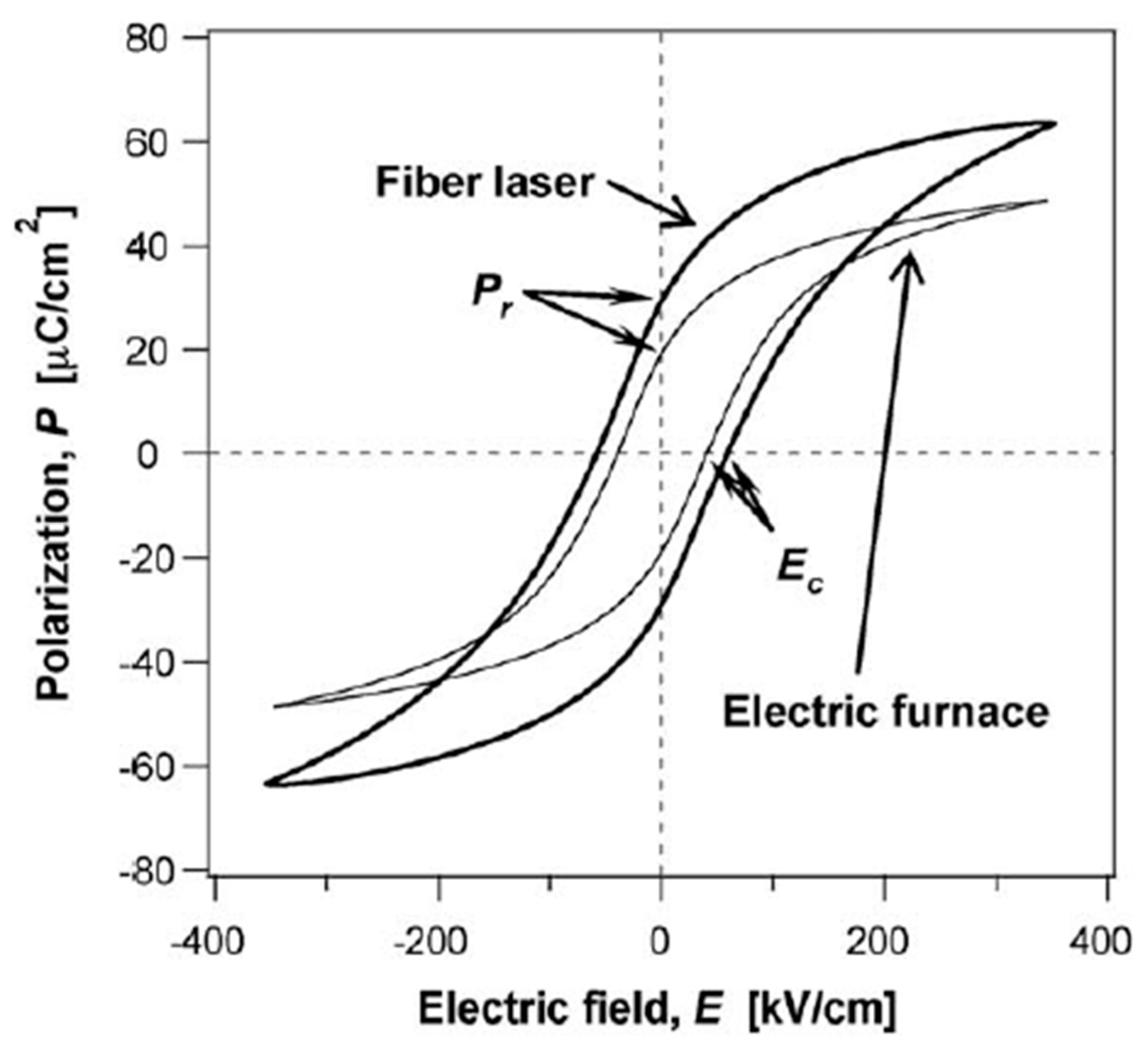
Investigations were also conducted by annealing the PZT/STS at 600 °C using an electric furnace (EF) and FL for comparison. Figure 11 presents the hysteresis loop of the PZT film annealed using EF and FL. As shown in Figure 11, the FL-annealed film exhibited a remnant polarization (Pr) value of 30 µC/cm2 and Ec < 50 kV/cm, which was significantly higher than that observed for the EF-annealed film [27].
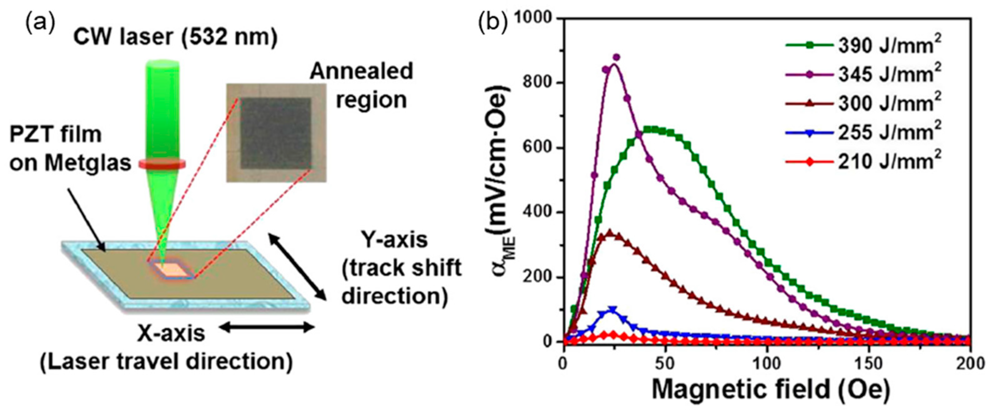
Palneedi et al. recently studied the effect of laser annealing on the magnetoelectric (ME) properties of PZT/Metglas (FeBSi amorphous alloy foil) heterostructured films grown via the GSV technique [28,29,30]. It is well known that PZT films deposited by the GSV method need to be annealed to achieve better piezoelectric performances; however, conventional annealing of the PZT film [31] on a low melting temperature Metglas (Tcrystal ≈ 510 °C) leads to the crystallization and oxidation of Metglas, resulting in the degradation of magnetostrictive properties. To overcome these problems, they [28] adopted localized annealing using continuous wave ytterbium (CW Yb) laser radiation (560 nm, 220 mW, and 0.05 mm/s), which was able to anneal the PZT thick film without causing any deteriorative effect to the Metglas. Most importantly, the dielectric, ferroelectric, and ME properties (Figure 12a) of the laser annealed PZT/Metglas system were greatly enhanced due to better crystallinity and grain growth in the PZT film owing to laser irradiation (Figure 12b). They [29] also investigated the effect of varying the laser energy (210–390 J/mm2, 0.1 mm/s) of a CW, neodymium-doped yttrium aluminum garnet laser (532 nm) on the ME properties of a 2-µm-thick PZT film deposited on Metglas. They found that the ME voltage coefficient of the PZT/Metglas system increases with laser energy up to 345 J/mm2 and decreases thereafter (Figure 12b). They observed that the properties of PZT and the ME coupling in PZT/Metglas were strongly dependent on changes in the crystallinity and grain size of the PZT film with a variation in laser intensity.
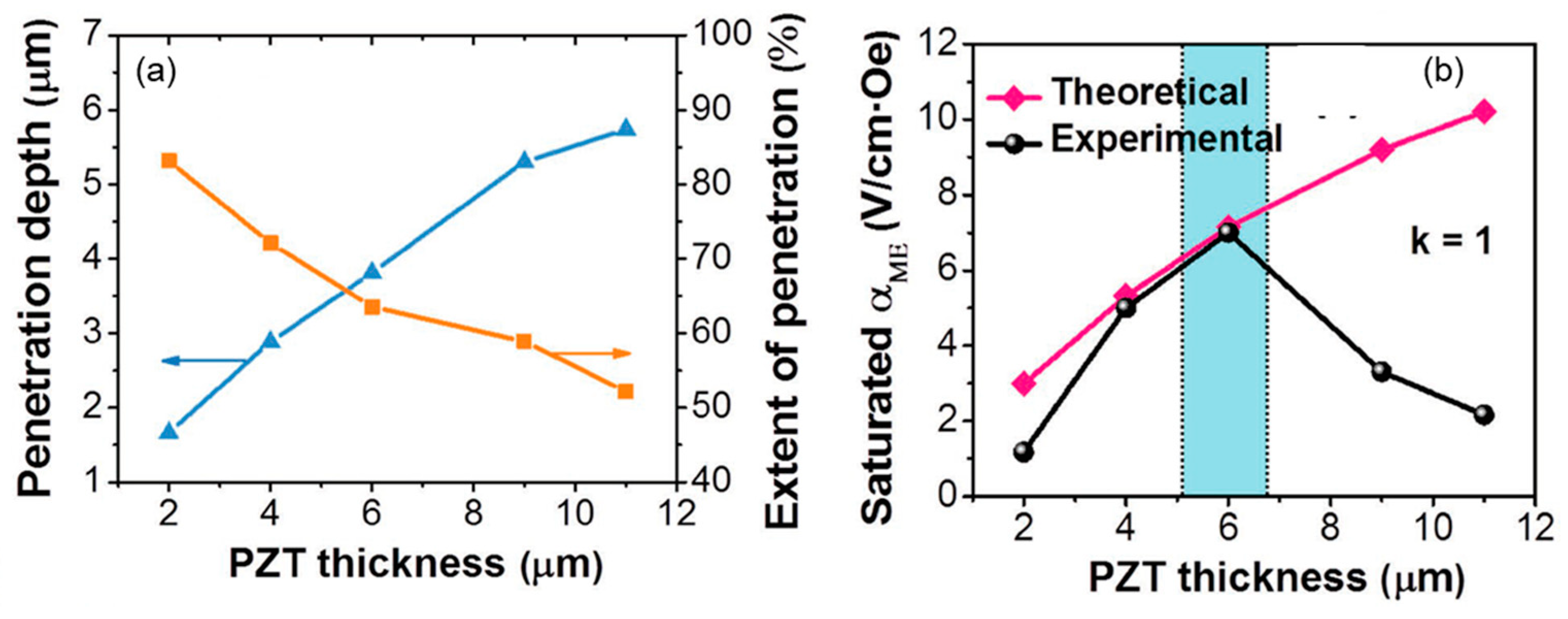
The effect of laser annealing on the ME properties of PZT films with different thicknesses (2–11 µm) was also studied [30]. The ME output was found to be strongly dependent on film thickness and the extent of film annealed via laser radiation (Figure 13a). Laser treatment could completely anneal the PZT films up to a thickness of 6 µm; beyond that, the films were only partially annealed. This is because the extent of penetration of laser radiation decreases with increasing PZT thickness (Figure 13a). The thicker films deposited via GSV contain a higher volume fraction of the amorphous phase and a smaller volume fraction of the nanocrystalline phase; consequently, the films exhibit a lower thermal conductivity, resulting in a constrained dissipation of laser-induced heat through the thicker films, which is insufficient to anneal the layers closer to the Metglas substrate. The PZT films with greater thicknesses can be completely annealed by using higher laser energy. A large ME output (comparable to the theoretical value) of 7 V/cm. Oe was obtained from laser-annealed PZT/Metglas film composites (Figure 13b).
3.4. Deposition of Lead-Free Piezoelectric Thick Films
Fabricating lead-free piezoelectric ceramic thick films is considerably challenging when using conventional film growth techniques due to the volatile nature of the elements involved, such as Bi, Na, and K. [8,32,33]. However, these thick films can be easily prepared via AD, which involves the processing of these thick films at RT with enhanced piezoelectric/ferroelectric responses. (K,N)aNbO3 (KNN) is one of the most promising materials owing to its excellent ferroelectric properties, low anisotropy, and high Curie temperature (Tc) [34,35]. A dense lead-free KNN piezoelectric film was deposited on a Si substrate and a Pt/Ti/SiO2/Si substrate at RT via AD. The as-deposited KNN film was annealed at 700 °C for 1 h. Scanning electron microscopy (SEM) images of the as-deposited and annealed KNN films are presented in Figure 14.
The primary concern with pristine KNN piezoelectric films is the difficulty in obtaining high-density sintered bodies through conventional processes and pressureless sintering due to the volatile nature of K and the instability of the crystal phase. It is possible to enhance the performance of pristine KNN films by lowering the phase transition from ferroelectric tetragonal to ferroelectric orthorhombic [33,36]. This can be achieved by adding LiSbO3 (LSO). The accelerated LSO-doped KNN particles collided with the Pt/TiO2/SiO2 substrate for the film at RT. The as-deposited KNN-LSO films were further annealed at 800 °C for 1 h to increase film crystallinity. The resultant SEM image of the KNN-LSO thick films is presented in Figure 15. The grain size of the annealed KNN-LSO was found to be 100 nm.
Figure 16 shows the P-E loop of the as-deposited and annealed KNN–LSO films. A paraelectric-like P-E loop was observed for the as-deposited KNN–LSO films, whereas symmetric hysteresis loops were observed for the annealed KNN–LSO films. Pr was found to be 15.5 µC/cm2, which was considerably higher than the value reported for KNN-based films [33]. Moreover, the Pr value of KNN increased by 90% with the addition of LSO, as compared with the pristine KNN film (Pr = 8 µC/cm2) [2], thereby indicating the superior piezoelectric properties of KNN–LSO films, which are beneficial for high-frequency ultrasonic transducers.
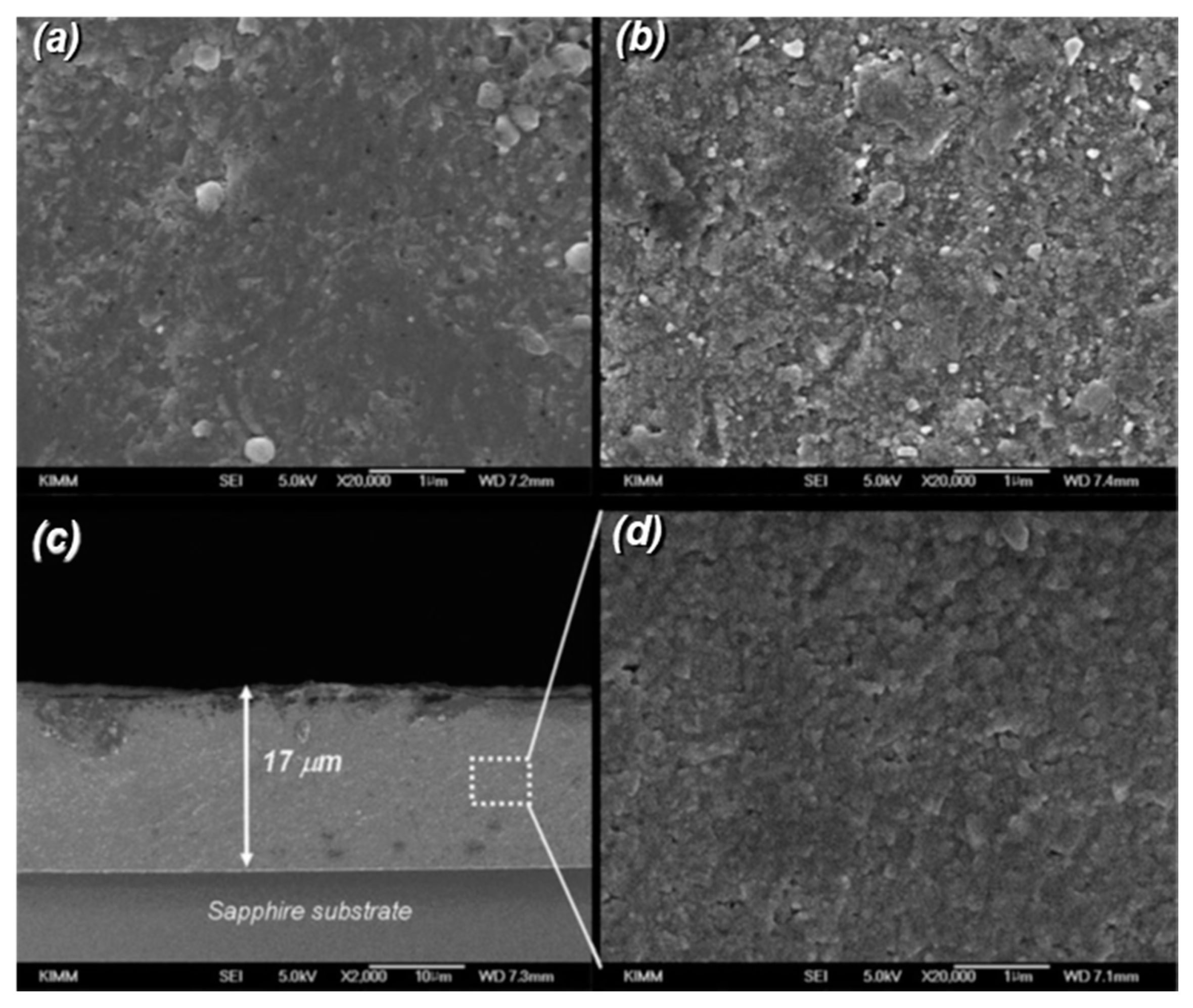
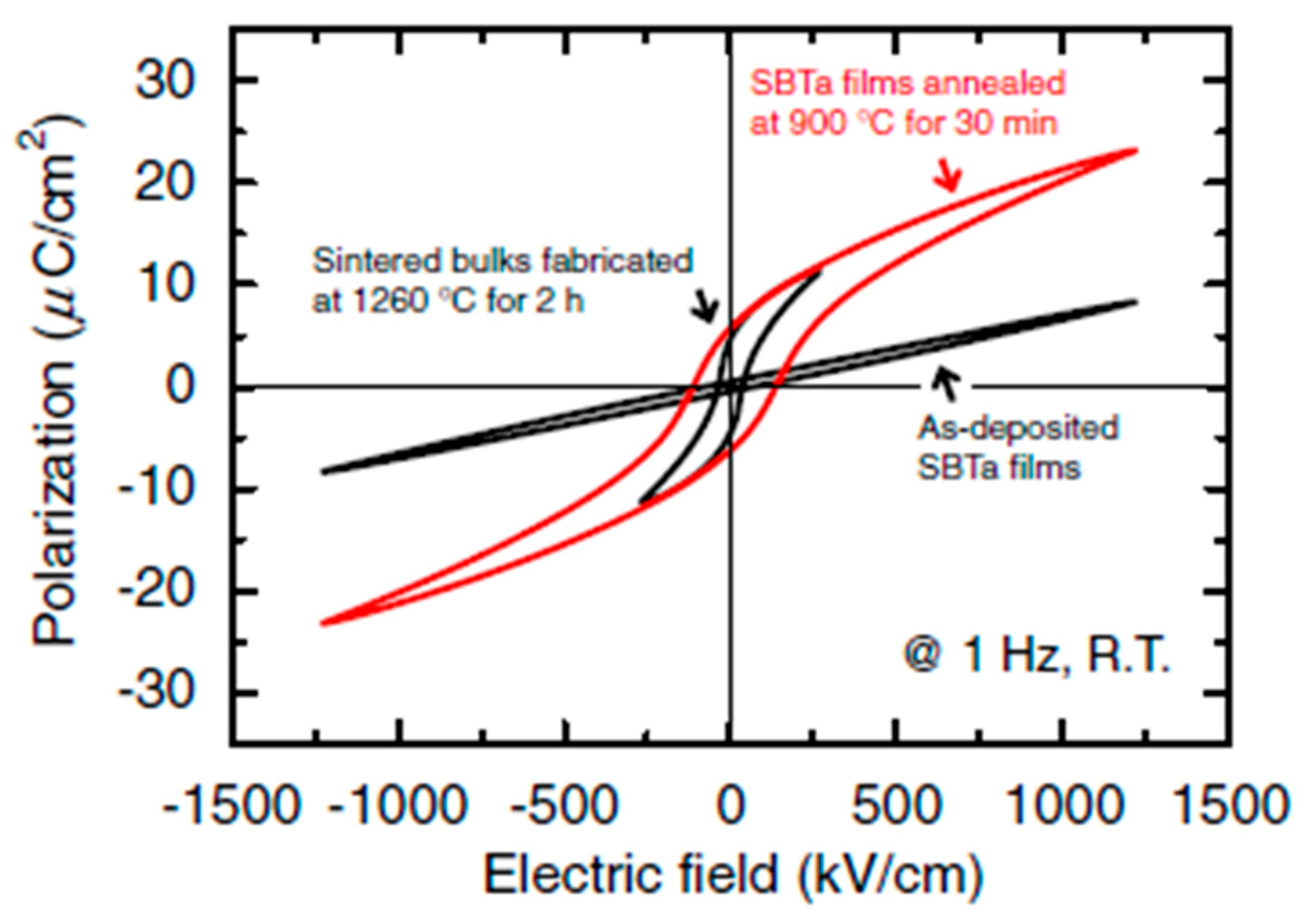
Bismuth strontium tantalate (SrBi2Ta2O9, SBTa ceramic films) exhibits a fatigue-free behavior [37]. SBTa and its related materials have been widely studied for their application in non-volatile ferroelectric random-access memories [38,39,40,41,42,43,44,45,46,47,48]. Ferroelectric thick films of SBTa were deposited on secured Pt/Ti/YSZ substrates via AD, and the as-deposited films were further annealed at 700–1100 °C for 30 min. For comparison, SBTa sintered bulks were also prepared using conventional solid-state reactions, employing the same starting raw powder used for AD.
Figure 17 shows the surface morphological SEM images of the as-deposited and annealed films on the Pt/Ti/YSZ substrate at different temperatures. It was reported that grain size increases in the subsequent annealing steps from 700–1100 °C in 200 °C intervals; this resultant growth occurs up to 300 nm. Finally, completely dense SBTa film microstructures are formed. Figure 18 presents the ferroelectric properties of the as-deposited and annealed films at 900 °C, as well as the sintered bulk. The films annealed at 900 °C yielded a Pr of 5.7 µC/cm2 and an Ec of 125 kV/cm, which are significantly higher than those of the sintered bulk (Pr of 4.7 µC/cm2 and Ec of 35.4 kV/cm). The large Pr value indicates that the vaporization of Bi is suppressed due to the minimum heat treatment required for AD-deposited films, which is of great importance in practical applications, whereas the sintering of bulk samples at high temperatures leads to Bi vaporization.
3.5. Micro-Patterning Materials Fabrication
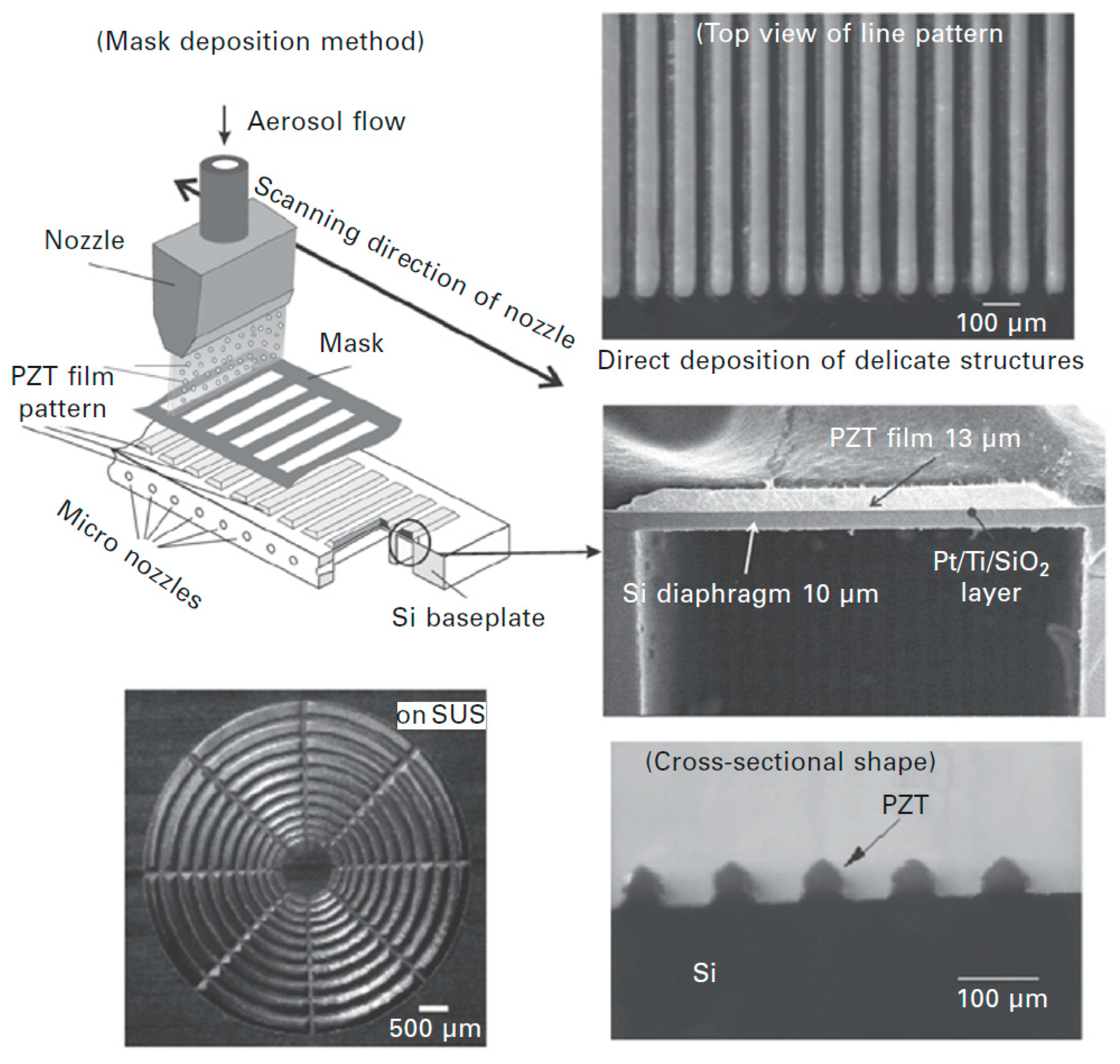
AD can also be used for film patterning via the mask deposition method [34,35], wherein the particle jet is impacted on the substrate through a defined pattern mask that contains openings with a width of at least 50 μm.
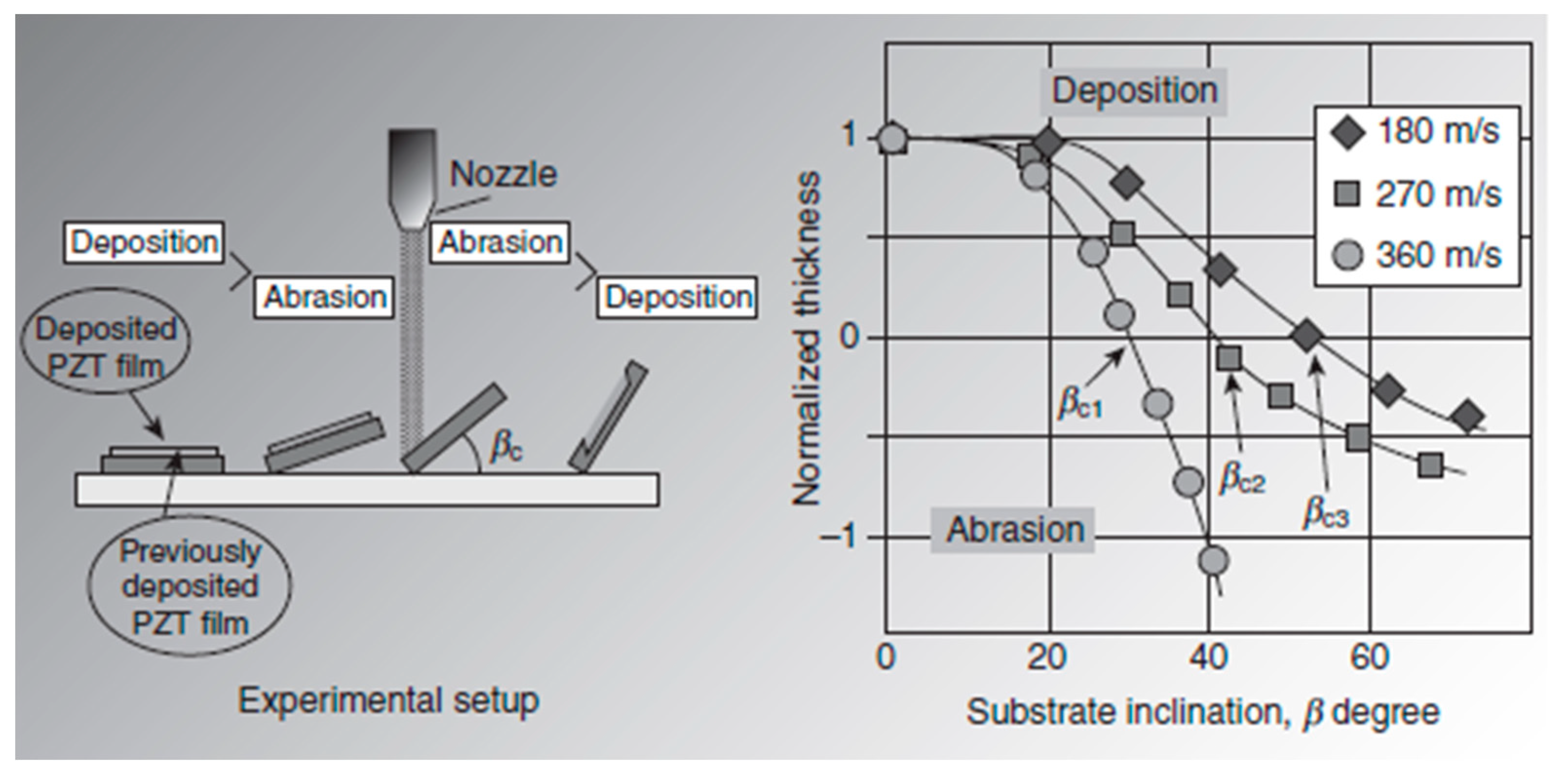
As shown in Figure 19, the effect of ceramic particles sprayed onto the substrate changes from deposition to erosion [2] depending on the velocity, particle diameter, and angle of incidence β of the particle jet on the substrate. At βc, the deposition and abrasion rates are equal, and the normalized thickness is that of the PZT layer after AD, relative to the initial value of PZT thickness. These factors also influence the layer density and surface roughness characteristics. However, to achieve acceptable patterns through a mask with sufficient detail, βc must be kept within a specified range. This is because βc affects the flow patterns, deposition efficiency, and the degree to which the mask profile is distorted.
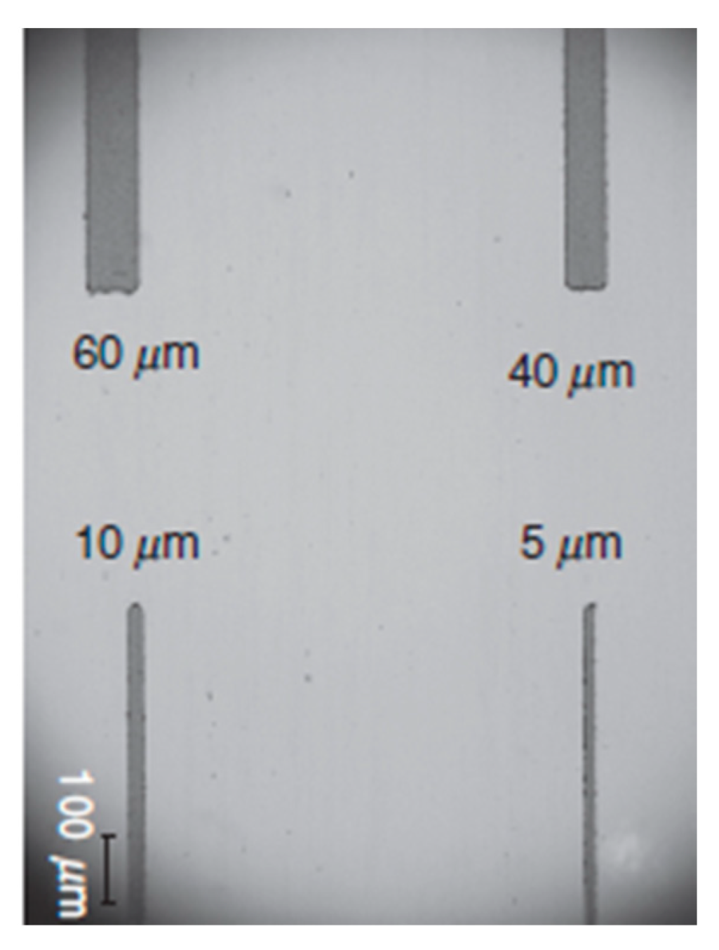
Figure 20 shows a thick, patterned PZT layer deposited onto stainless steel, silicon, and Pt/Si substrates under optimum conditions [2]. A thick film with a 50-μm-linewidth and an aspect ratio (line-height/linewidth) of >1 can be easily patterned by controlling the properties of the starting particle and the substrate temperature. It is difficult to obtain a pattern width of 50 μm on AD-deposited 10-μm-thick PZT films. However, the AD process is subsequently accompanied by the lift-off process. which makes this possible. For this purpose, the thickness and hardness of the photoresist layer should be chosen very carefully. A minimum pattern width of <10 μm on 2-μm-thick PZT and α–Al2O3 layers were successfully obtained, as shown in Figure 21.
4. Applications
4.1. Electro-Optic Probes
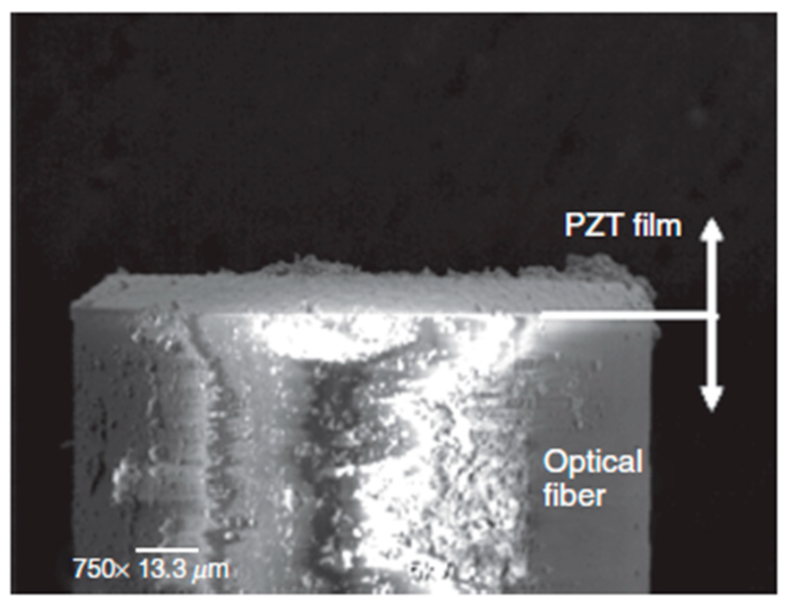
Iwanami et al. developed an electro-optic field probe [50] by depositing a 5-μm-thick PZT film onto an optical fiber edge with a length of 125 μm using AD, as shown in Figure 22. The probe was able to measure radiofrequency electro-optical signals over a microstrip line. They also studied the frequency response of the probe, which revealed its capability to measure fields in the range of gigahertz. The minimum measurable voltage sensitivity was found to be 50 mV/Hz1/2. The probe exhibits considerable potential for detailed semiconductor testing, the optimization of LSI packaging, and manufacturing reliability improvement.
4.2. Flapper Actuators for Hard Disk Drives
Flapper actuators are used in high-density hard disk drives (HDDs) for high-speed tracking and positioning of the magnetic head [51,52,53]. The process of writing data bits entails moving the magnetic head over the magnetic disk surface. The magnetic disk is spun, and the writing head, which is fixed at the head arm on the other end through a suspension beam, is placed over it. The recording density can be enhanced by increasing the number of data tracks along the disk radius. However, it becomes considerably challenging to appropriately place and aligns the magnetic head on top of the disk using conventional voice coil servo motors. This difficulty can be eliminated by employing actuator-based magnetic head controllers. The utilization of a microactuator attached between the suspension beam and the slider makes it easier to control the movement of the magnetic head within the range of ±1 µm with high speed and accuracy.
PZT thick films were directly deposited on a stainless steel STS304 substrate via AD. The obtained actuators had a length of 1.5–10 mm and width of 1 mm. The accuracy of the 3-mm-long actuator in terms of positioning the magnetic head under an applied potential of 5 V was found to be limited by the sensitivity of the measuring apparatus. The characteristics of the PZT/STS cantilever (19/50 μm) with a length of 10 mm were investigated by applying a unipolar voltage (50 V at 0.04 kHz). This was followed by the recalculation and comparison of results with the corresponding data of a more real actuator structure and applied conditions (cantilever length = 3 mm; same PZT/STS thickness; and applied potential of 5 V at 1 kHz). The obtained amplitude of deflection and measured inaccuracy of positioning were 0.5 μm and 20 nm, respectively, which are satisfactory for controlling the position of the magnetic head. Thus, the AD-derived PZT/STS cantilever is a cost-efficient actuator that exhibits good fatigue and linear frequency properties. Additionally, the inaccuracy in positioning lies within the acceptable range. Hence, the PZT/STS actuator is applicable for the positioning of magnetic heads in new-generation HDDs.
4.3. Optical Modulators
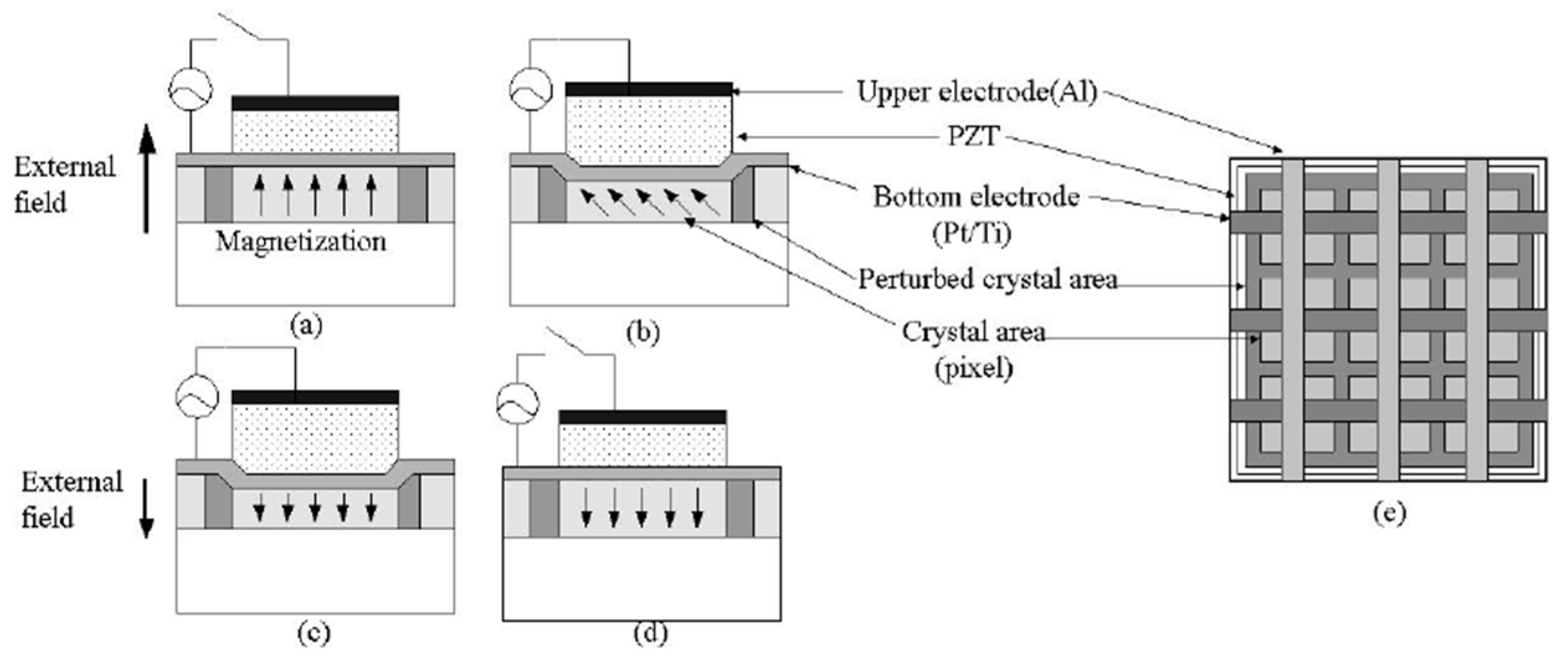
A spatial light modulator (SLM) is used to modify the polarization, amplitude, and phase of the optical wavefront via an electrically controlled signal. Different types of SLMs with pixel arrays have been developed thus far. A magneto-optic SLM (MOSLM) offers the advantages of high switching speed, non-volatility, and robustness. However, conventional MOSLMs consume significant amounts of power and require large driving currents. To overcome these disadvantages, the MOSLM is developed using a PZT driven by an electric and a magnetic field. A PZT-based MOSLM prototype was fabricated by incorporating a piezoelectric thick film into a magneto-optic material.
4.3.1. Mechanism of PZT-Driven MOSLM
Magnetization is induced upon the application of stress to a magnetic material. The effective magnetic field is derived by the following equation [54]:
where Mg, λ, and σ are the saturation magnetization, magnetostriction, and stress, respectively.
4.3.2. Construction and Working
Figure 23a presents an initial saturation magnetization of the bismuth-substituted yttrium/iron garnet (Bi:YIG) layer under an applied bias field. When voltage is applied to the PZT layer, it generates stress in the Bi:YIG layer according to Equation (1). The stress generated by the PZT layer changes the magnetization of the Bi:YIG layer according to the magnetostriction effect. In the Bi:YIG pixel, the stress generated by the PZT is equivalent to the effective magnetic field Heff [55] (Figure 23b). By changing the direction of the external field, the magnetization of the Bi:YIG layer can be easily reversed. (Figure 23c). Finally, the direction of magnetization is kept reversed by turning off the external field (Figure 23d).
The novel PZT-MOSLM is driven by the generation of a piezoelectric effect in the AD-deposited PZT film by applying an electric field rather than a magnetic field, which helps to reduce the anisotropic energy of the Bi:YIG layer. The pixels could be easily switched in the presence of a small external bias field. On using AD-deposited PZT films, there was a drastic reduction in power consumption, as compared to that of the current-driven MOSLM. Pixel switching at 20 MHz was successfully achieved by applying a driving voltage of 8 V.
4.4. Ultrasonic Motors
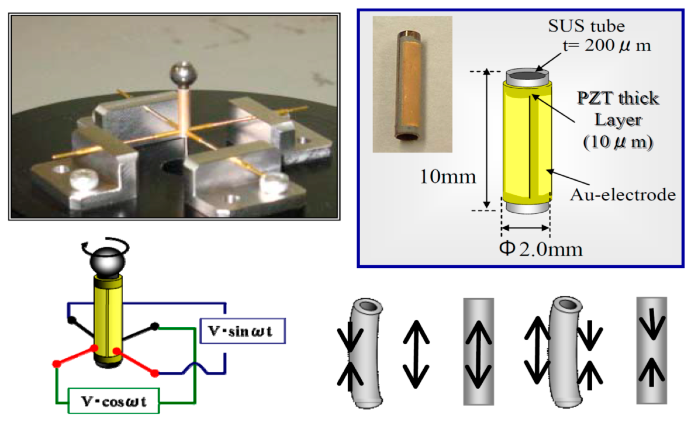
Miniaturized electromagnetic motors (>1 cm3) with sufficient energy efficiency are rather difficult to fabricate. Therefore, a new class of motors, referred to as ultrasonic motors, has been attracting significant attention. Ultrasonic motors comprising piezoelectric materials whose efficiencies are insensitive to size and are superior in the mini-motor area. Tube-type prototypes of ultrasonic micromotors were fabricated via AD, as shown in Figure 24 [2]. In this motor, a 10-μm-thick PZT film was deposited on the curved surface of a 2-mm-diameter stainless steel tube by means of AD. The rotation speed of the motor was found to be approximately 1200–1500 rpm, for a driving voltage of approximately 7–15 V.
4.5. Mechanical Energy Harvesting
Considering the ability of AD to fabricate dense thick films at RT, it has been applied for piezoelectric materials in energy harvesting technology [1,11,16,17,18,57,58,59,60]. Piezoelectric materials, such as PZT [61], aluminum-nitride [62], zirconate oxide [63], and KNN [64], have been widely used in MEMS energy harvesters. Specifically, PZT has been subjected to tremendous research due to its superior piezoelectric properties [18]. However, AD-fabricated films need to be heat treated in order to achieve large grain sizes (>1 μm) for high piezoelectric activity [65,66]. Therefore, the deposited films are typically annealed to promote grain growth [18,19,67]. Conventional annealing methods are unsuitable for annealing some of the flexible substrates used in energy harvesting [68]. Therefore, new approaches have been explored to overcome this challenge, which include the separation of deposited films from the original substrate through laser annealing.
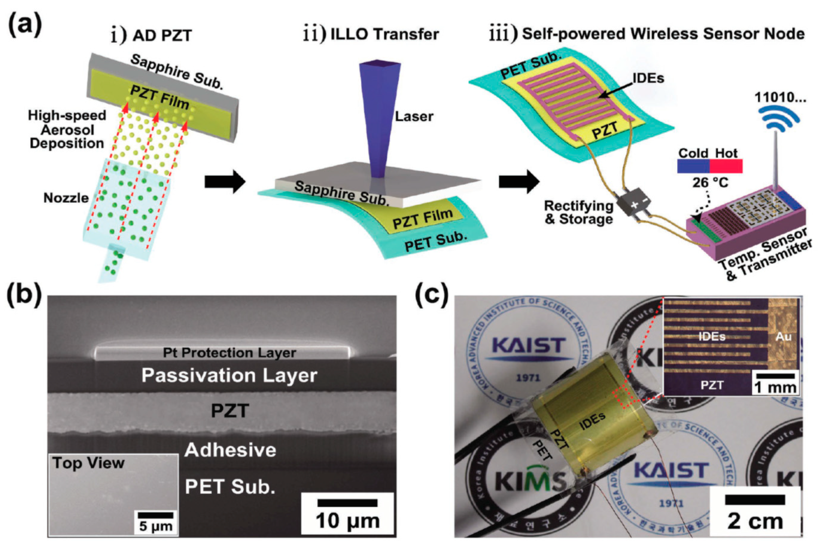
Recently, Hwang et al. described a technique called inorganic-based laser lift-off (ILLO) for separating piezoelectric AD-PZT films from their original substrates [69]. A film deposited on a sapphire substrate was successfully separated by irradiating the backside of the sapphire substrate with a XeCl laser (308 nm, and photon energy of 4.03 eV). Laser energy could not penetrate the sapphire substrate due to its wide bandgap (10 eV) and only couples in the interface between the PZT and sapphire to locally vaporize the PZT material (band gap energy 3.3 eV) [55,70]. After separation, the PZT film is transferred to a flexible polyethylene terephthalate (PET) substrate. Hwang et al. reported a single-step deposition of PZT films on sapphire substrates using AD, and post-annealing was employed to fabricate a high-performance, flexible piezoelectric energy harvester. The annealed film was transferred to a flexible substrate via the ILLO process (Figure 25). The flexible PZT harvester could generate a maximum output voltage of 200 V and a current of 35 mA from biomedical bending motions. The generated electricity was used to operate a wireless Internet of Things sensor 18 times [69].
Kuo et al. fabricated a bimorph vibration energy harvester based on cantilever beams where a seismic mass at the tip of the cantilever beam generates periodic vibrations in a piezoelectric layer to produce an output voltage [71]. Kuo et al. achieved a maximum power of 423 μW at an excitation frequency of 143.4 Hz using an excitation acceleration of 1.5 g. The bimorph piezoelectric MEMS generator poled for serial connection was driven up to a base excitation acceleration of 1.5 g and connected with an optimal load impedance of 330 kΩ. The device poled for serial connection achieved a maximum power output of 413 μW and an output voltage of 33 Vp-p under a 1.5 g base excitation acceleration.
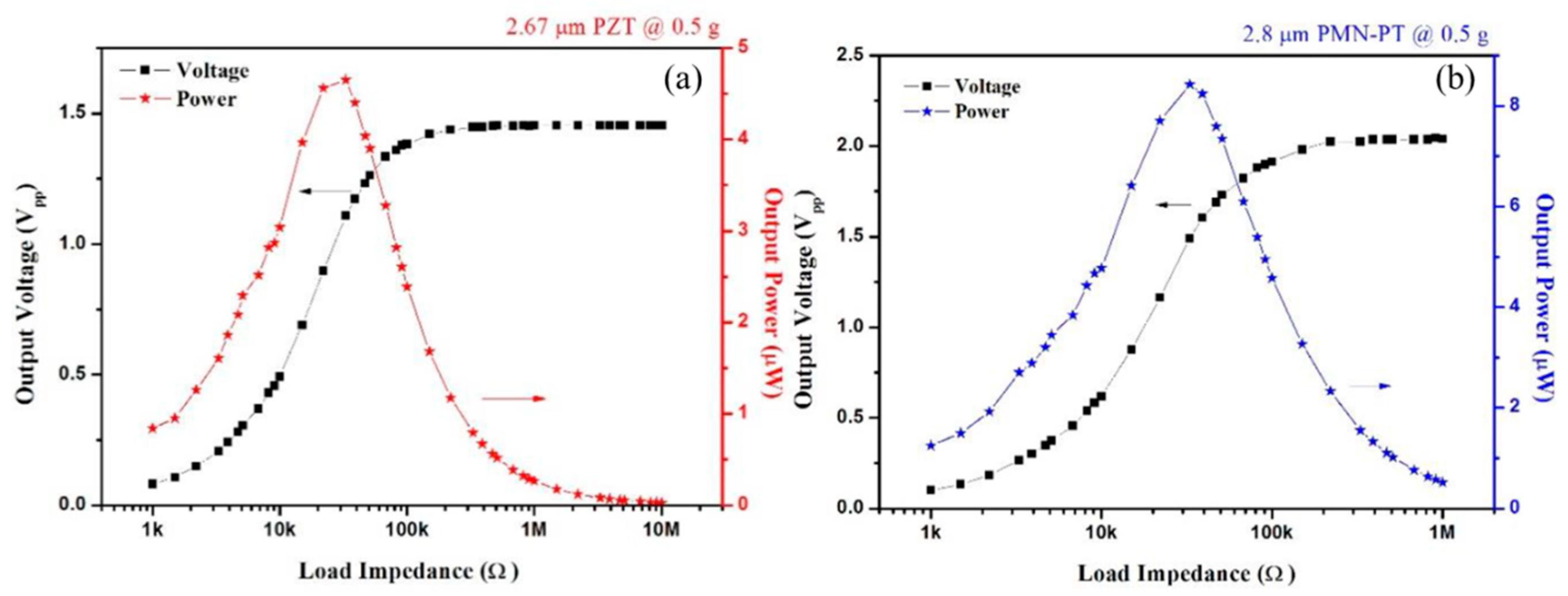
Chen et al. conducted a comparative study between the AD-PZT and lead magnesium niobate-lead titanate (PMN-PT) energy harvesters (EH). Their experimental results showed that the PZT-based EH achieved a maximum output power of 4.65 μW with a 1.11 Vpp output voltage under a 0.5 g base excitation, whereas the PMN-PT-based device yielded a maximum output power of 8.42 μW with a 1.49 Vpp output voltage at the same base excitation level (Figure 26). Thus, the PMN-PT-based EH has an output power 1.8 times greater than that of traditional PZT-based EHs [64].
4.6. Optical Micro Scanner
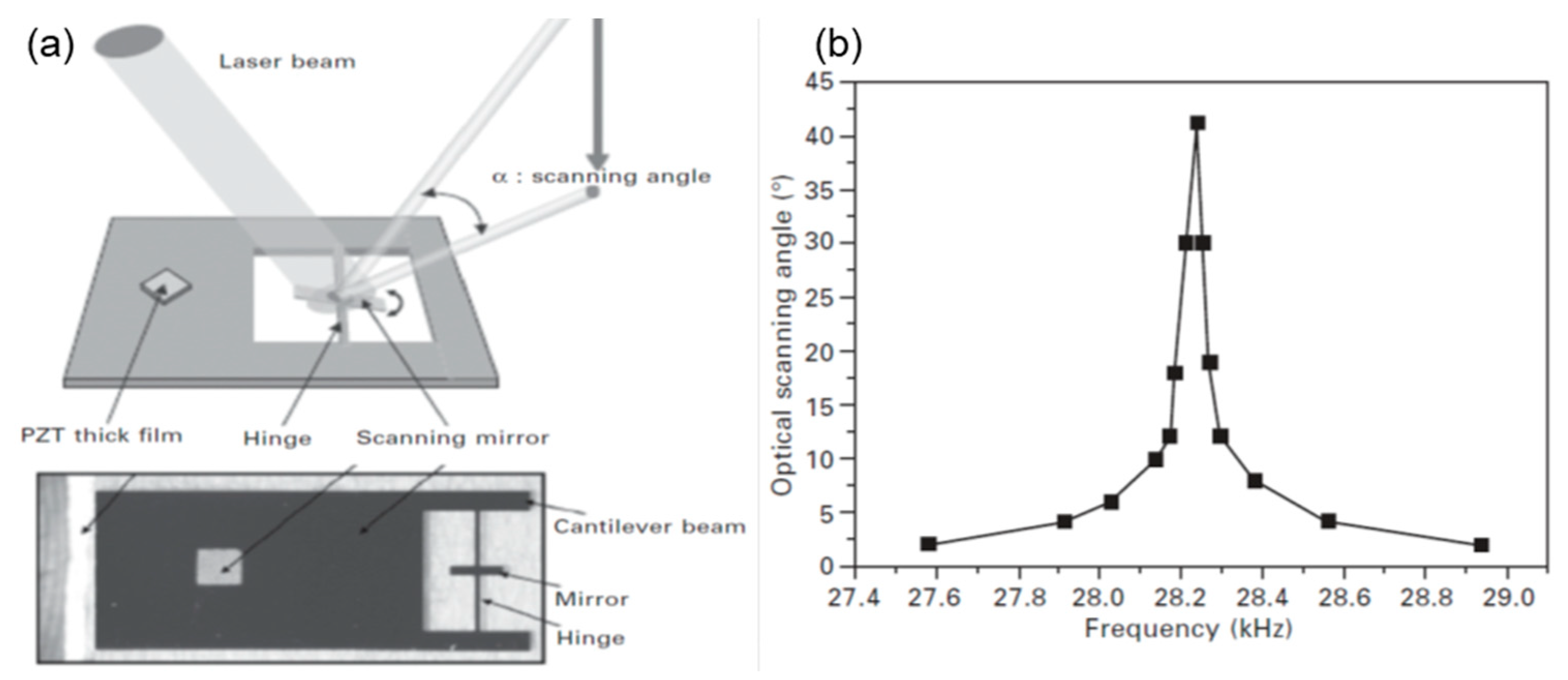
A typical optical micro scanner comprises two hinges, a reflection mirror, a mainframe, two cantilever beams, an excitation source (PZT thick film), and a clamping holder (Figure 27a). The mirror is sustained by using two cantilevers, a torsion bar, and a connecting beam between them. PZT actuators are fabricated on cantilevers to actuate the scanner. These actuators are also driven at the resonance frequency of the scanner by applying sine-voltages to generate bending moments of the beams, which are then converted to torque for rotating the mirror [72]. The laser beam is incident on the reflection mirror, whereas the reflected beam is projected on the photodiode. The mirror is scanned by applying a sine voltage, and the trajectory of the scanning beam is used to calculate the scan angle [72]. The d31 mode of the piezoelectric actuator bends the scanner frame to induce vibrational ‘‘Lamb wave’’ within the frame. The metal scanner structure is specially designed, two-dimensionally guided, and concentrated the lamb waves towards the narrow torsion hinges holding the mirror. The waves change with the torsional vibrations of the mirror caused by the vertical difference in the direction between progressing waves and the torsion hinge. Moreover, the torsional vibration vertically scans the mirror axis.
For the optical micro scanner, a silicon wafer and stainless steel were used as the substrates. Generally, stainless steel is preferred in optical scanners due to its robust structure, as compared to silicon. A 6-μm-thick PZT film deposited on a Si wafer using AD and annealed at 600 °C for 1 h was used for the optical micro scanner. Using this device, a scanning angle of 25.9° was achieved using a driving voltage of 60 V, at a resonance frequency of 33 kHz [72]; this was similar to the scanners composed of stainless steel. Using AD-PZT films with a thickness of 5–20 μm, a scanning angle of up to 42° was realized with a driving voltage of 60 V, at the resonance frequency of approximately 28 kHz (Figure 27b) [73,74]. The scanning angle and frequency can be easily adjusted by modifying the mirror size and hinge length.
4.7. Ultrasonic Transducers
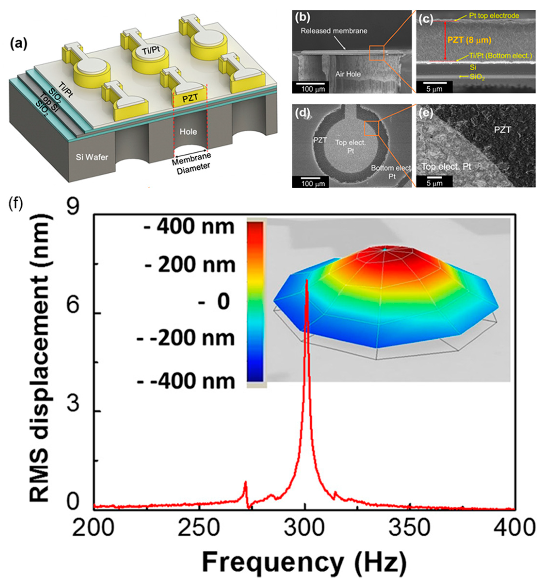
Piezoelectric micro-machined ultrasonic transducers (pMUTs) have attracted significant attention owing to their potential applications in ultrasonic cameras, intravascular ultrasound systems, and portable medical diagnosis systems. pMUTs are superior to conventional ultrasonic transducers in terms of their low power consumption, acoustic impedance matching with the body, small size, and simple system integration. However, the thin, active piezoelectric films used for pMUTs are unable to produce sufficient acoustic pressure, resulting in weak ultrasonic intensities. Jung et al. overcame this limitation by fabricating a thick piezoelectric PZT film-based pMUT possessing high deflection at low driving voltages, by using AD [68]. Pre-patterned, highly dense PZT thick films (exceeding 8 μm) were grown on 6-in-diameter Si/SiO2/Ti/Pt wafers at RT, following the MEMS process (Figure 28a–e). The fabrication of pMUTs via GSV was considerably easy and fast, as compared to those prepared using the sol-gel process. The pMUT evinced a coupling coefficient of 1.05% and exhibited a high peak displacement of 0.8 μm under 5 Vpp (E = 6.25 kVpp/cm), at its resonance frequency of 300.9 kHz (Figure 28b).
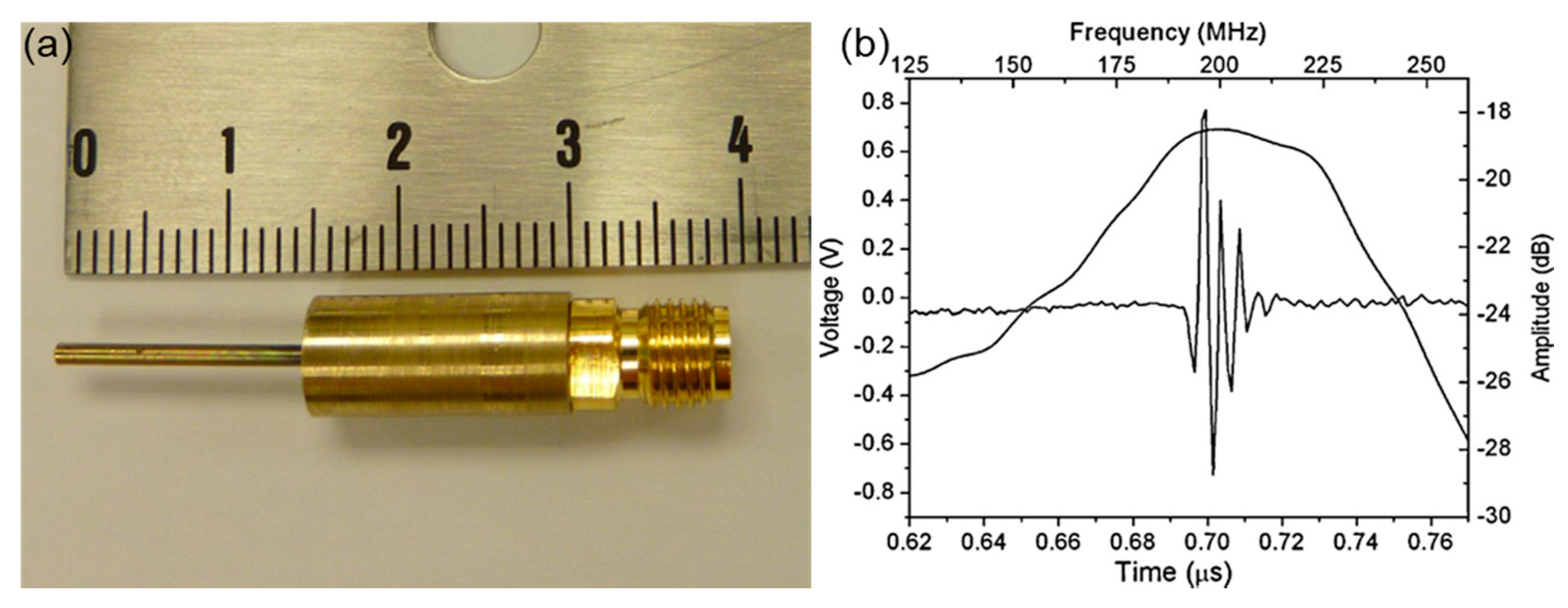
Similarly, Lau et al. reported the fabrication of a 194-MHz high-frequency needle transducer using a lead-free 0.948(K0.5Na0.5)NbO3-0.052LiSbO3 film as an active element [75]. They first deposited 6-μm-thick KNN-LSO on a platinized Si substrate via GSV (Figure 29a). A dense and crack-free thick film was fabricated, which exhibited an excellent remnant polarization of 13.2 μC/cm2 and dielectric constant of 766. A needle transducer comprising the KNN-LSO thick film exhibited a center frequency of 197 MHz with a bandwidth at −6 dB, approximately 50% with a -20 dB pulse length of 20 ns (Figure 29b). The performance of this lead-free needle transducer is comparable to that of the PZT-based transducer.
4.8. Energy Storage Capacitors
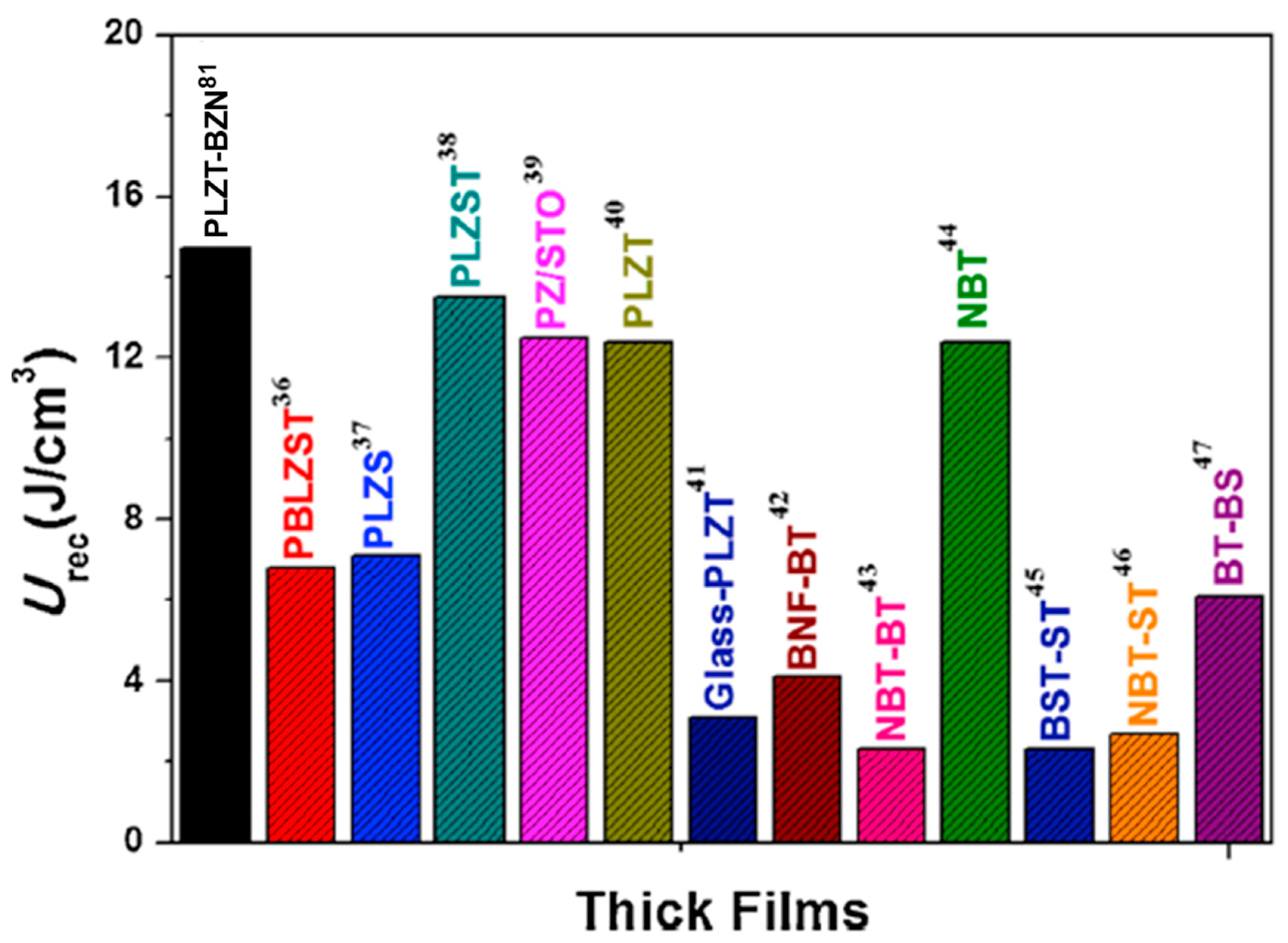
Recently, capacitors with considerably high energy density and high efficiency have attracted significant research attention for various applications such as hybrid electric automobiles, military ordnance, and smart electronics. Energy storage capacity is associated with low dielectric loss, high breakdown strength, low Pr, and maximum polarization (Pmax). Generally, relaxor ferroelectrics are highly ideal candidates for energy storage due to their narrow hysteresis (low hysteresis loss), which is attributed to their high-density microstructure with nano-sized domains. AD produces highly dense materials featuring nano-sized grains. With regard to this, Park et al. fabricated nano-sized grained ferroelectric 65PMN-35PT thick films for a high energy density capacitor [76]. AD films of 65PMN-35PT exhibited a narrower hysteresis loop than that of the bulk with the same composition, along with increased energy storage. Furthermore, AD films exhibit a smaller loss than bulk materials (Figure 30a,b). The energy density (U) and efficiency (η) were calculated from the hysteresis loop by using and η = U/(U + Uloss), respectively. Therefore, low loss and enhanced breakdown are required to achieve high energy efficiency. Similarly, high Pmax and Emax and low Pr and Ec are needed for U and η [76]. After annealing, the AD film of 65PMN-35PT revealed a U of 35 J/cc and η of 70% at a 2000 kV/cm electric field (Figure 30c). Kang et al. [77] also reported a temperature-independent energy density for PIN-PMN-PT thick films fabricated via AD. Jung et al. [78] reported a high recoverable U for Pb0.92La0.08Zr0.52Ti0.48O3- Bi(Zn0.66Nb0.33O3) (PLZT-BZN) mixed systems fabricated via the AD process. They studied the effect of different compositions and annealing temperatures on U and η. The PLZT-BZN5 film annealed at 550 °C exhibited a superior U of 14.7 J/cm3 under an electric field of 1400 kV/cm and an η of 81% with low dielectric loss and improved temperature stability. The recoverable U of the PLZT-BZN5 film was considerably higher than that of other reported thick films (Figure 31). Similarly, a few lead-free thick films have also been fabricated via the AD process for energy storage applications [79,80,81].
5. Summary
Herein, the primary features of the AD technique for obtaining high-quality piezoelectric thick films and their applications to various devices are discussed. The deposition mechanism, general aspects of AD, structural and ferroelectric/piezoelectric properties, and its potential applications were introduced and discussed in comparison with conventional thin film technologies. Relative to conventional film processes, AD features unique processing capabilities, such as lower annealing temperature, higher deposition rate, dense film fabrication at RT, the withholding of primary material composition, and a crystal structure in the deposited films, due to the RT impact consolidation process.
Some of the salient features of this method are as follows:
- (a)
- Dense consolidation of ceramic microparticles is realized at RT.
- (b)
- Film formation in the AD process can be explained using a five-step process: Spraying >> impact >> Cracking >> Densification >> Consolidation.
- (c)
- The piezoelectric properties of lead-based thick films deposited via AD were discussed, along with the effects of low-temperature post-annealing of these thick films. The piezoelectric properties of PZT thick films were enhanced significantly after post-annealing the as-deposited AD films.
- (d)
- AD is capable of fabricating complex ferroelectric thick films, such as lead-free KNN and SBTa, featuring enhanced piezoelectric responses.
- (e)
- AD is considerably effective in fabricating functional piezoelectric materials for applications in micro-devices.
- (f)
- The improved version of AD, i.e., GSV, which is capable of producing a uniform and large-area deposition, is also introduced. GSV involves the intentional crushing of ceramic microparticles into fine particles.
- (g)
- AD/GSV is capable of depositing more than 100-μm-thick films with superior piezoelectric performances.
- (h)
- A few examples of piezoelectric and optical devices fabricated using AD were presented, and the advantages offered by this technique were highlighted.
Author Contributions
Conceptualization, D.R.P. and V.A.; methodology, D.R.P.; software, A.T.; validation, A.T. and J.K.; investigation, J.R.; writing—original draft preparation, D.R.P. and V.A.; writing—review and editing, J.R.; visualization, J.A.; supervision, J.R. All authors have read and agreed to the published version of the manuscript.
Funding
This research was funded by the National Research Foundation of Korea (NRF-2019R1A2B5B01070100). VA would like to acknowledge the support from the Department of Science and Technology (DST, Grant No. DST/INSPIRE/04/2016/001295) and the Science and Engineering Research Board (SERB, Grant No. SERB/F/7249/2019-2020), Government of India).
Conflicts of Interest
The authors declare no conflict of interest.
References
- Akedo, J.; Park, J.H.; Kawakami, Y. Piezoelectric thick film fabricated with aerosol deposition and its application to piezoelectric devices. Jpn. J. Appl. Phys. 2018, 57, 07LA02. [Google Scholar] [CrossRef]
- Akedo, J. Room temperature impact consolidation (RTIC) of fine ceramic powder by aerosol deposition method and applications to microdevices. J. Therm. Spray Technol. 2008, 17, 181–198. [Google Scholar] [CrossRef]
- Schubert, M.; Hanft, D.; Nazarenus, T.; Exner, J.; Schubert, M.; Nieke, P.; Glosse, P.; Leupold, N.; Kita, J.; Moos, R. Powder Aerosol Deposition Method-Novel Applications in the Field of Sensing and Energy Technology. Funct. Mater. Lett. 2019, 1930005. [Google Scholar] [CrossRef] [Green Version]
- Masafumi, N.; Toshihiro, K.; Mizuki, I.; Keishi, O. Application of Electronic Devices for Aerosol Deposition Methods. NEC TECH J. 2007, 2, 76–80. [Google Scholar]
- Kawakami, Y.; Aisawa, S.; Akedo, J. Annealing effect on 0.5Pb(Ni1/3Nb2/3)O3-0.5Pb(Zr0.3Ti0.7)O3 thick film deposited by aerosol deposition method. Jpn. J. Appl. Phys. Part 1 Regul. Pap. Short Notes Rev. Pap. 2005, 44, 6934–6937. [Google Scholar] [CrossRef]
- Kawakami, Y.; Watanabe, M.; Arai, K.I.; Sugimoto, S. Effects of substrate materials on piezoelectric properties of BaTiO3 thick films deposited by aerosol deposition. Proc. Jpn. J. Appl. Phys. 2016, 55. [Google Scholar] [CrossRef]
- Popovici, D.; Tsuda, H.; Akedo, J. Postdeposition annealing effect on (Ba0.6, Sr0.4)TiO3 thick films deposited by aerosol deposition method. J. Appl. Phys. 2009, 105, 061638. [Google Scholar] [CrossRef]
- Ryu, J.; Choi, J.J.; Hahn, B.D.; Park, D.S.; Yoon, W.H.; Kim, K.H. Fabrication and ferroelectric properties of highly dense lead-free piezoelectric (K0.5Na0.5)NbO3 thick films by aerosol deposition. Appl. Phys. Lett. 2007, 90, 152901. [Google Scholar] [CrossRef]
- Schubert, M.; Exner, J.; Moos, R. Influence of Carrier Gas Composition on the Stress of Al2O3 Coatings Prepared by the Aerosol Deposition Method. Materials 2014, 7, 5633–5642. [Google Scholar] [CrossRef] [Green Version]
- Kauffmann-Weiss, S.; Hassler, W.; Guenther, E.; Scheiter, J.; Denneler, S.; Glosse, P.; Berthold, T.; Oomen, M.; Arndt, T.; Stocker, T.; et al. Superconducting Properties of Thick Films on Hastelloy Prepared by the Aerosol Deposition Method with Ex Situ MgB2 Powder. IEEE Trans. Appl. Supercond. 2017, 27. [Google Scholar] [CrossRef]
- Akedo, J.; Lebedev, M. Microstructure and electrical properties of lead zirconate titanate (Pb(Zr52/Ti48)O3) thick films deposited by aerosol deposition method. Jpn. J. Appl. Phys. Part 1 Regul. Pap. Short Notes Rev. Pap. 1999, 38, 5397–5401. [Google Scholar] [CrossRef]
- Nam, S.M.; Mori, N.; Kakemoto, H.; Wada, S.; Akedo, J.; Tsurumi, T. Alumina thick films as integral substrates using aerosol deposition method. Jpn. J. Appl. Phys. Part 1 Regul. Pap. Short Notes Rev. Pap. 2004, 43, 5414–5418. [Google Scholar] [CrossRef]
- Sato, Y.; Uemichi, Y.; Nishikawa, K.; Yoshikado, S. Fabrication of Al2O3 Films Using Aerosol Deposition Method and Their Characterization. IOP Conf. Ser. Mater. Sci. Eng. 2011, 18, 092056. [Google Scholar] [CrossRef]
- Kim, J.; Lee, J.I.; Park, D.S.; Park, E.S. Enhancement of interface anchoring and densification of Y2O3 coating by metal substrate manipulation in aerosol deposition process. J. Appl. Phys. 2015, 117, 014903. [Google Scholar] [CrossRef] [Green Version]
- Akedo, J. Aerosol Deposition of Ceramic Thick Films at Room Temperature: Densification Mechanism of Ceramic Layers. J. Am. Ceram. Soc. 2006, 89, 1834–1839. [Google Scholar] [CrossRef]
- Akedo, J.; Lebedev, M. Aerosol Deposition Method (ADM): A novel method of PZT thick films producing for microactuators. Recent Res. Dev. Mater. Sci. 2001, 2, 51–77. [Google Scholar]
- Uchino, K. Advanced Piezoelectric Materials; Elsevier: Amsterdam, The Netherlands, 2010. [Google Scholar]
- Akedo, J.; Lebedev, M. Piezoelectric properties and poling effect of Pb(Zr,Ti)O3 thick films prepared for microactuators by aerosol deposition. Appl. Phys. Lett. 2000, 77, 1710–1712. [Google Scholar] [CrossRef]
- Akedo, J.; Lebedev, M. Effects of annealing and poling conditions on piezoelectric properties of Pb(Zr0.52,Ti0.48)O3 thick films formed by aerosol deposition method. J. Cryst. Growth 2002, 235, 415–420. [Google Scholar] [CrossRef]
- Ryu, J.; Han, G.; Song, T.K.; Welsh, A.; Trolier-Mckinstry, S.; Choi, H.; Lee, J.P.; Kim, J.W.; Yoon, W.H.; Choi, J.J.; et al. Upshift of phase transition temperature in nanostructured PbTiO3 thick film for high temperature applications. ACS Appl. Mater. Interfaces 2014, 6, 11980–11987. [Google Scholar] [CrossRef]
- Lee, J.; Lee, S.; Choi, M.-G.; Ryu, J.; Lee, J.-P.; Lim, Y.-S.; Jeong, D.-Y. Stress Modulation and Ferroelectric Properties of Nanograined PbTiO3 Thick Films on the Different Substrates Fabricated by Aerosol Deposition. J. Am. Ceram. Soc. 2014, 97, 3872–3876. [Google Scholar] [CrossRef]
- Hahn, B.D.; Kim, K.H.; Park, D.S.; Choi, J.J.; Ryu, J.; Yoon, W.H.; Park, C.; Kim, D.Y. Fabrication of lead zirconate titanate thick films using a powder containing organic residue. Jpn. J. Appl. Phys. 2008, 47, 5545–5552. [Google Scholar] [CrossRef]
- Han, G.; Ryu, J.; Yoon, W.-H.; Choi, J.-J.; Hahn, B.-D.; Park, D.-S. Effect of Film Thickness on the Piezoelectric Properties of Lead Zirconate Titanate Thick Films Fabricated by Aerosol Deposition. J. Am. Ceram. Soc. 2011, 94, 1509–1513. [Google Scholar] [CrossRef]
- Ryu, J.; Priya, S.; Park, C.S.; Kim, K.Y.; Choi, J.J.; Hahn, B.D.; Yoon, W.H.; Lee, B.K.; Park, D.S.; Park, C. Enhanced domain contribution to ferroelectric properties in freestanding thick films. J. Appl. Phys. 2009, 106, 024108. [Google Scholar] [CrossRef] [Green Version]
- Lebedev, M.; Akedo, J. Patterning Properties of Lead Zirconate Titanate (PZT) Thick Films Made by Aerosol Deposition. IEEJ Trans. Sens. Micromachines 2000, 120, 600–601. [Google Scholar] [CrossRef] [Green Version]
- Han, G.; Ryu, J.; Yoon, W.H.; Choi, J.J.; Hahn, B.D.; Kim, J.W.; Park, D.S.; Ahn, C.W.; Priya, S.; Jeong, D.Y. Stress-controlled Pb(Zr0.52Ti0.48)O3 thick films by thermal expansion mismatch between substrate and Pb(Zr0.52Ti0.48)O3 film. J. Appl. Phys. 2011, 110, 124101. [Google Scholar] [CrossRef] [Green Version]
- Baba, S.; Akedo, J. Fiber laser annealing of nanocrystalline PZT thick film prepared by aerosol deposition. Appl. Surf. Sci. 2009, 255, 9791–9795. [Google Scholar] [CrossRef]
- Palneedi, H.; Maurya, D.; Kim, G.Y.; Priya, S.; Kang, S.J.L.; Kim, K.H.; Choi, S.Y.; Ryu, J. Enhanced off-resonance magnetoelectric response in laser annealed PZT thick film grown on magnetostrictive amorphous metal substrate. Appl. Phys. Lett. 2015, 107, 012904. [Google Scholar] [CrossRef]
- Palneedi, H.; Maurya, D.; Kim, G.Y.; Annapureddy, V.; Noh, M.S.; Kang, C.Y.; Kim, J.W.; Choi, J.J.; Choi, S.Y.; Chung, S.Y.; et al. Unleashing the Full Potential of Magnetoelectric Coupling in Film Heterostructures. Adv. Mater. 2017, 29, 1–9. [Google Scholar] [CrossRef]
- Palneedi, H.; Choi, I.; Kim, G.-Y.; Annapureddy, V.; Maurya, D.; Priya, S.; Kim, J.-W.; Lee, K.J.; Choi, S.-Y.; Chung, S.-Y.; et al. Tailoring the Magnetoelectric Properties of Pb(Zr,Ti)O3 Film Deposited on Amorphous Metglas Foil by Laser Annealing. J. Am. Ceram. Soc. 2016, 99, 2680–2687. [Google Scholar] [CrossRef]
- Im, I.-H.; Chung, K.-H.; Kim, D.-H. Dependence of Annealing Temperature on Properties of PZT Thin Film Deposited onto SGGG Substrate. Trans. Electr. Electron. Mater. 2014, 15, 253–256. [Google Scholar] [CrossRef]
- Oh, S.W.; Akedo, J.; Park, J.H.; Kawakami, Y. Fabrication and evaluation of lead-free piezoelectric ceramic LF4 thick film deposited by aerosol deposition method. Jpn. J. Appl. Phys. Part 1 Regul. Pap. Short Notes Rev. Pap. 2006, 45, 7465–7470. [Google Scholar] [CrossRef]
- Ryu, J.; Choi, J.J.; Hahn, B.D.; Park, D.S.; Yoon, W.H. Ferroelectric and piezoelectric properties of 0.948(K0.5Na0.5)NbO3-0.052LiSbO3 lead-free piezoelectric thick film by aerosol deposition. Appl. Phys. Lett. 2008, 92, 012905. [Google Scholar] [CrossRef]
- Maeder, M.D.; Damjanovic, D.; Setter, N. Lead free piezoelectric materials. In Proceedings of the Journal of Electroceramics; Springer: Berlin/Heidelberg, Germany, 2004; Volume 13, pp. 385–392. [Google Scholar]
- Saito, Y.; Takao, H.; Tani, T.; Nonoyama, T.; Takatori, K.; Homma, T.; Nagaya, T.; Nakamura, M. Lead-free piezoceramics. Nature 2004, 432, 84–87. [Google Scholar] [CrossRef] [PubMed]
- Zhang, S.; Xia, R.; Shrout, T.R.; Zang, G.; Wang, J. Piezoelectric properties in perovskite 0.948(K0.5Na0.5)NbO3-0.052LiSbO3 lead-free ceramics. J. Appl. Phys. 2006, 100, 104108. [Google Scholar] [CrossRef]
- De Araujo, C.A.P.; Cuchiaro, J.D.; Mc Millan, D.L.; Scott, M.C.; Scott, J.F. Fatigue-free ferroelectric capacitors with platinum electrodes. Nature 1995, 374, 627–629. [Google Scholar] [CrossRef]
- Noguchi, Y.; Miyayama, M.; Kudo, T. Direct evidence of A-site-deficient strontium bismuth tantalate and its enhanced ferroelectric properties. Phys. Rev. B Condens. Matter Mater. Phys. 2001, 63, 214102. [Google Scholar] [CrossRef]
- Atsuki, T.; Soyama, N.; Yonezawa, T.; Ogi, K. Preparation of bi-based ferroelectric thin films by sol-gel method. Jpn. J. Appl. Phys. 1995, 34, 5096–5099. [Google Scholar] [CrossRef]
- Noguchi, T.; Hase, T.; Miyasaka, Y. Analysis of the dependence of ferroelectric properties of strontium bismuth tantalate (SBT) thin films on the composition and process temperature. Jpn. J. Appl. Phys. Part 1 Regul. Pap. Short Notes Rev. Pap. 1996, 35, 4900–4904. [Google Scholar] [CrossRef]
- Noda, M.; Matsumuro, Y.; Sugiyama, H.; Okuyama, M. A fatigue-tolerant metal-ferroelectric-oxide-semiconductor structure with large memory window using Sr-deficient and Bi-excess Sr0.7Bi2+yTa2O9 ferroelectric films prepared on SiO2/Si at low temperature by pulsed laser deposition. Jpn. J. Appl. Phys. Part 1 Regul. Pap. Short Notes Rev. Pap. 1999, 38, 2275–2280. [Google Scholar] [CrossRef]
- Furuya, A.; Cuchiaro, J.D. Compositional Dependence of Electrical Characteristics in SrBi2Ta2-xNbxO9 Ferroelectric Capacitor Reduced by H2 Annealing. Jpn. J. Appl. Phys. 2000, 39, L371–L373. [Google Scholar] [CrossRef]
- Forbess, M.J.; Seraji, S.; Wu, Y.; Nguyen, C.P.; Cao, G.Z. Dielectric properties of layered perovskite Sr1-xAxBi2Nb2O9 ferroelectrics (A=La, Ca and x=0,0.1). Appl. Phys. Lett. 2000, 76, 2934–2936. [Google Scholar] [CrossRef]
- Aizawa, K.; Tokumitsu, E.; Okamoto, K.; Ishiwara, H. Impact of face-to-face annealing in preparation of sol-gel-derived SrBi2Ta2O9 thin films. Appl. Phys. Lett. 2000, 76, 2609–2611. [Google Scholar] [CrossRef]
- Chung, H.-T.; Cho, J.-H.; Kim, H.-G. The Effect of Bi Ions Substituting at the Sr Site in SrBi2Ta2O9. Jpn. J. Appl. Phys. 1998, 37, 2554–2558. [Google Scholar] [CrossRef]
- Shimakawa, Y.; Kubo, Y.; Nakagawa, Y.; Kamiyama, T.; Asano, H.; Izumi, F. Crystal structures and ferroelectric properties of SrBi2Ta2O9 and Sr0.8Bi2.2Ta2O9. Appl. Phys. Lett. 1999, 74, 1904–1906. [Google Scholar] [CrossRef]
- Noguchi, Y.; Miyayama, M.; Kudo, T. Effect of Bi substitution at the Sr site on the ferroelectric properties of dense strontium bismuth tantalate ceramics. J. Appl. Phys. 2000, 88, 2146–2148. [Google Scholar] [CrossRef]
- Shoji, K.; Aikawa, M.; Uehara, Y.; Sakata, K. Preparation and Properties of SrBi2Ta2O9 Ceramics. Jpn. J. Appl. Phys. 1998, 37, 5273–5276. [Google Scholar] [CrossRef]
- Suzuki, M.; Nishihara, Y.; Uesu, Y.; Akedo, J. Polarization properties of bismuth strontium tantalate ceramic films deposited by aerosol deposition method. Jpn. J. Appl. Phys. 2012, 51, 09LA17. [Google Scholar] [CrossRef]
- Iwanami, M.; Nakada, M.; Tsuda, H.; Ohashi, K.; Akedo, J. Ultra small electro-optic field probe fabricated by aerosol deposition. IEICE Electron. Express 2007, 4, 26–32. [Google Scholar] [CrossRef] [Green Version]
- Nojima, Y.; Koganezawa, S. Newly Designed Slider-Based Micro-Actuator for Magnetic Disk Drive. J. Adv. Mech. Des. Syst. Manuf. 2011, 5, 45–53. [Google Scholar] [CrossRef]
- Hirano, T.; Fan, L.S.; Lee, W.Y.; Hong, J.; Imaino, W.; Pattanaik, S.; Chan, S.; Webb, P.; Horowitz, R.; Aggarwal, S.; et al. High-bandwidth high-accuracy rotary microactuators for magnetic hard disk drive tracking servos. IEEE/ASME Trans. Mechatronics 1998, 3, 156–165. [Google Scholar] [CrossRef]
- Lebedev, M.; Akedo, J. Thick PZT film/stainless steel actuator fabricated by aerosol deposition method: Fatigue property. In Proceedings of the Nano-and Microtechnology: Materials, Processes, Packaging, and Systems; Sood, D.K., Malshe, A.P., Maeda, R., Eds.; SPIE: Melbourne, Australia, 2002; Volume 4936, p. 345. [Google Scholar]
- Schröder, K. Stress operated random access, high-speed magnetic memory. J. Appl. Phys. 1982, 53, 2759–2761. [Google Scholar] [CrossRef]
- Robertson, J.; Warren, W.L. Energy levels of point defects in perovskite oxides. In Proceedings of the Materials Research Society Symposium-Proceedings. Mater. Res. Soc. 1995, 361, 123–128. [Google Scholar] [CrossRef]
- Takagi, H.; Park, J.H.; Mizoguchi, M.; Nishimura, K.; Uchida, H.; Lebedev, M.; Akedo, J.; Inoue, M. PZT-driven micromagnetic optical devices. In Proceedings of the Materials Research Society Symposium-Proceedings; Cambridge University Press: Cambridge, UK, 2003; Volume 785, pp. 177–182. [Google Scholar]
- Akedo, J.; Kiyohara, M. Nanostructuring by Shock Compaction with Fine Particle Beam. J. Soc. Powder Technol. Jpn. 2003, 40, 192–200. [Google Scholar] [CrossRef]
- Akedo, J.; Lebedev, M.; Iwata, A.; Ogiso, H.; Nakano, S. Aerosol Deposition Method (Adm) For Nano-Crystal Ceramics Coating Without Firing. MRS Online Proc. Libr. Arch. 2003, 778. [Google Scholar] [CrossRef]
- Akedo, J.; Lebedev, M. Powder preparation in aerosol deposition method for lead zirconate titanate thick films. Jpn. J. Appl. Phys. Part 1 Regul. Pap. Short Notes Rev. Pap. 2002, 41, 6980–6984. [Google Scholar] [CrossRef]
- Lebedev, M.; Akedo, J.; Mori, K.; Eiju, T. Simple self-selective method of velocity measurement for particles in impact-based deposition. J. Vac. Sci. Technol. A Vac. Surf. Film. 2000, 18, 563–566. [Google Scholar] [CrossRef]
- Fang, H.B.; Liu, J.Q.; Xu, Z.Y.; Dong, L.; Wang, L.; Chen, D.; Cai, B.C.; Liu, Y. Fabrication and performance of MEMS-based piezoelectric power generator for vibration energy harvesting. Microelectron. J. 2006, 37, 1280–1284. [Google Scholar] [CrossRef]
- Elfrink, R.; Kamel, T.M.; Goedbloed, M.; Matova, S.; Hohlfeld, D.; Van Andel, Y.; Van Schaijk, R. Vibration energy harvesting with aluminum nitride-based piezoelectric devices. J. Micromechanics Microengineering 2009, 19. [Google Scholar] [CrossRef] [Green Version]
- Trolier-Mckinstry, S.; Muralt, P. Thin film piezoelectrics for MEMS. J. Electroceramics 2004, 12, 7–17. [Google Scholar] [CrossRef]
- Chaoting, C.; Wu, W.-J.; Chen, C.T.; Lin, S.C.; Lin, T.K.; Wu, W.J. High-performance energy harvester fabricated with aerosol deposited PMN-PT material. Artic. J. Phys. Conf. Ser. 2016. [Google Scholar] [CrossRef] [Green Version]
- Hanft, D.; Exner, J.; Schubert, M.; Stöcker, T.; Fuierer, P.; Moos, R. An overview of the Aerosol Deposition method: Process fundamentals and new trends in materials applications. J. Ceram. Sci. Technol. 2015, 6, 147–181. [Google Scholar]
- Heywang, W.; Lubitz, K.; Wersing, W. Piezoelectricity; Springer Series in Materials Science; Springer: Berlin/Heidelberg, Germany, 2008; p. 114. [Google Scholar]
- Hahn, B.D.; Park, D.S.; Choi, J.J.; Yoon, W.H.; Ryu, J.; Kim, D.Y. Effects of Zr/Ti ratio and post-annealing temperature on the electrical properties of lead zirconate titanate (PZT) thick films fabricated by aerosol deposition. J. Mater. Res. 2008, 23, 226–235. [Google Scholar] [CrossRef]
- Jung, J.; Annapureddy, V.; Hwang, G.T.; Song, Y.; Lee, W.; Kang, W.; Ryu, J.; Choi, H. 31-mode piezoelectric micromachined ultrasonic transducer with PZT thick film by granule spraying in vacuum process. Appl. Phys. Lett. 2017, 110, 212903. [Google Scholar] [CrossRef]
- Hwang, G.T.; Annapureddy, V.; Han, J.H.; Joe, D.J.; Baek, C.; Park, D.Y.; Kim, D.H.; Park, J.H.; Jeong, C.K.; Park, K.-I.; et al. Self-Powered Devices: Self-Powered Wireless Sensor Node Enabled by an Aerosol-Deposited PZT Flexible Energy Harvester. Adv. Energy Mater. 2016, 6. [Google Scholar] [CrossRef] [Green Version]
- Do, Y.H.; Kang, M.G.; Kim, J.S.; Kang, C.Y.; Yoon, S.J. Fabrication of flexible device based on PAN-PZT thin films by laser lift-off process. Sens. Actuators A Phys. 2012, 184, 124–127. [Google Scholar] [CrossRef]
- Kuo, C.-L.; Lin, S.-C.; Wu, W.-J. Fabrication and performance evaluation of a metal-based bimorph piezoelectric MEMS generator for vibration energy harvesting. Smart Mater. Struct. 2016, 25, 105016. [Google Scholar] [CrossRef]
- Asai, N.; Matsuda, R.; Watanabe, M.; Takayama, H.; Yamada, S.; Mase, A.; Shikida, M.; Sato, K.; Lebedev, M.; Akedo, J. A novel high resolution optical scanner actuated by aerosol deposited PZT films. In Proceedings of the IEEE Micro Electro Mechanical Systems (MEMS), Kyoto, Japan, 23 January 2003; pp. 247–250. [Google Scholar]
- Park, J.H.; Akedo, J.; Sato, H. High-speed metal-based optical microscanners using stainless-steel substrate and piezoelectric thick films prepared by aerosol deposition method. Sens. Actuators A Phys. 2007, 135, 86–91. [Google Scholar] [CrossRef]
- Akedo, J.; Lebedev, M.; Sato, H.; Park, J. High-speed optical microscanner driven with resonation of lam waves using Pb(Zr,Ti)O3 thick films formed by aerosol deposition. Jpn. J. Appl. Phys. Part 1 Regul. Pap. Short Notes Rev. Pap. 2005, 44, 7072–7077. [Google Scholar] [CrossRef]
- Lau, S.T.; Li, X.; Zhou, Q.F.; Shung, K.K.; Ryu, J.; Park, D.S. Aerosol-deposited KNN-LSO lead-free piezoelectric thick film for high frequency transducer applications. Sens. Actuators A Phys. 2010, 163, 226–230. [Google Scholar] [CrossRef]
- Park, C.K.; Lee, S.H.; Lim, J.H.; Ryu, J.; Choi, D.H.; Jeong, D.Y. Nano-size grains and high density of 65PMN-35PT thick film for high energy storage capacitor. Ceram. Int. 2018, 44, 20111–20114. [Google Scholar] [CrossRef]
- Kang, S.B.; Kim, H.S.; Lee, J.G.; Park, C.K.; Ryu, J.; Choi, J.J.; Hahn, B.D.; Wang, L.; Jeong, D.Y. Dielectric properties of Pb(In1/2Nb1/2)O3-Pb(Mg1/3Nb2/3)O3-PbTiO3 film by aerosol deposition for energy storage applications. Ceram. Int. 2016, 42, 1740–1745. [Google Scholar] [CrossRef]
- Jung, H.B.; Lim, J.H.; Peddigari, M.; Ryu, J.; Choi, D.H.; Jeong, D.Y. Enhancement of energy storage and thermal stability of relaxor Pb0.92La0.08Zr0.52Ti0.48O3-Bi(Zn0.66Nb0.33)O3 thick films through aerosol deposition. J. Eur. Ceram. Soc. 2020, 40, 63–70. [Google Scholar] [CrossRef]
- Kim, J.-W.; Lim, J.H.; Kim, S.H.; Koo, C.Y.; Ryu, J.; Jeong, D.Y. Energy storage properties of dielectric Bi1.5Zn1.0Nb1.5O7 thick films on flexible metal foil substrates fabricated by aerosol deposition method. J. Ceram. Process. Res. 2018, 19, 243. [Google Scholar]
- Lim, J.H.; Lee, S.H.; Kim, K.H.; Ji, S.Y.; Jung, S.; Park, C.K.; Jung, H.B.; Jeong, D.Y. High temperature grain growth behavior of aerosol deposited BaTiO3 film on (100), (110) oriented SrTiO3 single crystal. Korean J. Mater. Res. 2019, 29, 684–689. [Google Scholar] [CrossRef]
- Lim, J.H.; Kim, J.W.; Lee, S.H.; Park, C.K.; Ryu, J.; Choi, D.H.; Jeong, D.Y. Fabrication of high density BZN-PVDF composite film by aerosol deposition for high energy storage properties. Korean J. Mater. Res. 2019, 29, 175–182. [Google Scholar] [CrossRef]
Figure 1.
Different applications of piezoelectric thick films with varying thicknesses.

Figure 2.
Piezoelectric film formation technologies and a comparison of piezoelectric properties.

Figure 3.
Improvement in the functional properties of ferroelectric aerosol deposition (AD) films by heat treatment [2]. © Copyright 2008, J. Therm. Spray Technol.
Figure 3.
Improvement in the functional properties of ferroelectric aerosol deposition (AD) films by heat treatment [2]. © Copyright 2008, J. Therm. Spray Technol.

Figure 4.
Schematic of AD apparatus.

Figure 5.
Typical transmission electron microscopy (TEM) image (cross-sectional) of a lead zirconate titanate (PZT) thick film deposited on Si substrate at room temperature (RT) via AD [11]. © Copyright 1999, Jpn. J. Appl. Phys.
Figure 5.
Typical transmission electron microscopy (TEM) image (cross-sectional) of a lead zirconate titanate (PZT) thick film deposited on Si substrate at room temperature (RT) via AD [11]. © Copyright 1999, Jpn. J. Appl. Phys.

Figure 6.
Field Emission Scanning Electron Microscope images of PZT thick films deposited from powder mixed with polyvinylidene fluoride (PVDF). (a,b), Cross-sectional and (c,d) surface microstructure images of PZT thick films [22]. © Copyright 2008, Jpn. J. Appl. Phys.
Figure 6.
Field Emission Scanning Electron Microscope images of PZT thick films deposited from powder mixed with polyvinylidene fluoride (PVDF). (a,b), Cross-sectional and (c,d) surface microstructure images of PZT thick films [22]. © Copyright 2008, Jpn. J. Appl. Phys.

Figure 7.
Polarization-electric field (P-E) hysteresis loops of 5-μm-thick PZT films (a) as-deposited and (b) after post-annealing at 600 °C with different particle impact velocities [17]. © Copyright 2010, Elsevier.
Figure 7.
Polarization-electric field (P-E) hysteresis loops of 5-μm-thick PZT films (a) as-deposited and (b) after post-annealing at 600 °C with different particle impact velocities [17]. © Copyright 2010, Elsevier.

Figure 8.
Schematic of high piezoelectric performance in PZT thick films deposited on various substrates; their stresses were controlled via the thermal expansion mismatch between substrates and PZT films [26]. © Copyright 2011, J. Appl. Phys.
Figure 8.
Schematic of high piezoelectric performance in PZT thick films deposited on various substrates; their stresses were controlled via the thermal expansion mismatch between substrates and PZT films [26]. © Copyright 2011, J. Appl. Phys.

Figure 9.
P-E hysteresis loops of annealed PZT films deposited on different substrates [26]. © Copyright 2011, J. Appl. Phys.
Figure 9.
P-E hysteresis loops of annealed PZT films deposited on different substrates [26]. © Copyright 2011, J. Appl. Phys.

Figure 10.
Photographs of top and bottom surfaces of PZT/ stainless-steel substrate (STS) system annealed using (a) fiber laser (FL) and (b) CO2 laser irradiations [27]. © Copyright 2009, ApplAppl. Surf. Sci.
Figure 10.
Photographs of top and bottom surfaces of PZT/ stainless-steel substrate (STS) system annealed using (a) fiber laser (FL) and (b) CO2 laser irradiations [27]. © Copyright 2009, ApplAppl. Surf. Sci.

Figure 11.
Comparative ferroelectric hysteresis loops of 10 µm thick AD PZT films annealed using an electric furnace (EF) at 600 °C and FL [27]. © Copyright 2009, ApplAppl. Surf. Sci.
Figure 11.
Comparative ferroelectric hysteresis loops of 10 µm thick AD PZT films annealed using an electric furnace (EF) at 600 °C and FL [27]. © Copyright 2009, ApplAppl. Surf. Sci.

Figure 12.
(a) Schematic of laser annealing of PZT/Metglas. (b) Variation of magnetoelectric (ME) voltage coefficient (αME) as a function of Hdc at a fixed AC magnetic field of 1 Oe at f = 1 kHz for laser annealed PZT/Metglas [30]. © Copyright 2016, J. Am. Ceram. Soc.
Figure 12.
(a) Schematic of laser annealing of PZT/Metglas. (b) Variation of magnetoelectric (ME) voltage coefficient (αME) as a function of Hdc at a fixed AC magnetic field of 1 Oe at f = 1 kHz for laser annealed PZT/Metglas [30]. © Copyright 2016, J. Am. Ceram. Soc.

Figure 13.
(a) Variation in laser penetration depth and extent of penetration as a function of PZT film thickness. (b) Effect of PZT film thickness on theoretical and experimental αME values [29]. © Copyright 2017, Adv. Mater.
Figure 13.
(a) Variation in laser penetration depth and extent of penetration as a function of PZT film thickness. (b) Effect of PZT film thickness on theoretical and experimental αME values [29]. © Copyright 2017, Adv. Mater.

Figure 14.
Scanning electron microscopy (SEM) images of the AD films (a) cross section, (b) as-deposited film, and (c) annealed (K,N)aNbO3 (KNN) film [8]. © Copyright 2007, Appl. Phys. Lett.
Figure 14.
Scanning electron microscopy (SEM) images of the AD films (a) cross section, (b) as-deposited film, and (c) annealed (K,N)aNbO3 (KNN) film [8]. © Copyright 2007, Appl. Phys. Lett.

Figure 15.
SEM images of the (a) as-deposited and (b) 800 °C-annealed KNN–LiSbO3 (LSO) films. (c) Low- and (d) high-magnification cross-sectional views of the annealed film [33]. © Copyright 2008, Appl. Phys. Lett.
Figure 15.
SEM images of the (a) as-deposited and (b) 800 °C-annealed KNN–LiSbO3 (LSO) films. (c) Low- and (d) high-magnification cross-sectional views of the annealed film [33]. © Copyright 2008, Appl. Phys. Lett.

Figure 16.
P-E hysteresis loop of the as-deposited and annealed KNN–LSO films [33]. © Copyright 2008, Appl. Phys. Lett.
Figure 16.
P-E hysteresis loop of the as-deposited and annealed KNN–LSO films [33]. © Copyright 2008, Appl. Phys. Lett.

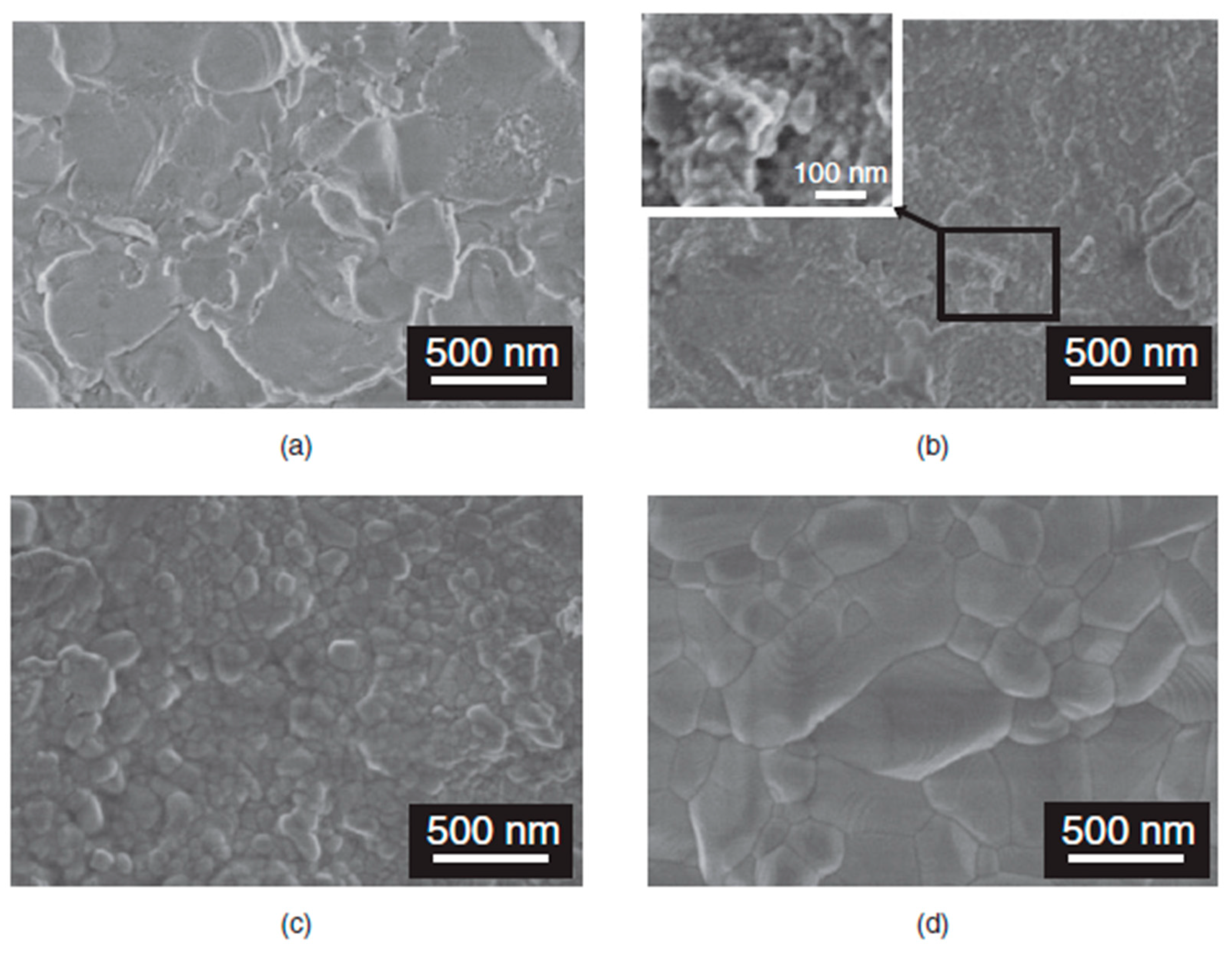
Figure 17.
SEM images of SrBi2Ta2O9 (SBTa) films deposited on Pt/Ti/yttria-stabilized zirconia (YSZ) ceramic substrates (a) as-deposited and annealed at (b) 700 °C for 30 min, (c) 900 °C for 30 min, and (d) 1100 °C for 30 min [49]. © Copyright 2012, Jpn. J. Appl. Phys. Lett.
Figure 17.
SEM images of SrBi2Ta2O9 (SBTa) films deposited on Pt/Ti/yttria-stabilized zirconia (YSZ) ceramic substrates (a) as-deposited and annealed at (b) 700 °C for 30 min, (c) 900 °C for 30 min, and (d) 1100 °C for 30 min [49]. © Copyright 2012, Jpn. J. Appl. Phys. Lett.

Figure 18.
P-E curves of AD films deposited on Pt/Ti/YSZ substrates and sintered bulk [49]. © Copyright 2012, Jpn. J. Appl. Phys. Lett.
Figure 18.
P-E curves of AD films deposited on Pt/Ti/YSZ substrates and sintered bulk [49]. © Copyright 2012, Jpn. J. Appl. Phys. Lett.

Figure 19.
Particle jet flow angle of incidence effect on deposition properties [2]. © Copyright 2008, J. Therm. Spray Technol.
Figure 19.
Particle jet flow angle of incidence effect on deposition properties [2]. © Copyright 2008, J. Therm. Spray Technol.

Figure 20.
Patterning of thick ceramic films via AD using the mask deposition method [2]. © Copyright 2008, J. Therm. Spray Technol.
Figure 20.
Patterning of thick ceramic films via AD using the mask deposition method [2]. © Copyright 2008, J. Therm. Spray Technol.

Figure 21.
Micro-patterning of piezoelectric layers deposited via AD using the lift-off process with photoresist [2]. © Copyright 2008, J. Therm. Spray Technol.
Figure 21.
Micro-patterning of piezoelectric layers deposited via AD using the lift-off process with photoresist [2]. © Copyright 2008, J. Therm. Spray Technol.

Figure 22.
SEM image of PZT-deposited optical fiber edge [50]. © Copyright 2007, IEICE Electron. Express.
Figure 22.
SEM image of PZT-deposited optical fiber edge [50]. © Copyright 2007, IEICE Electron. Express.

Figure 23.
Schematics of PZT-driven magneto-optic spatial light modulator (MOSLM) and the switching mechanism of magnetization in the bismuth-substituted yttrium/iron garnet (Bi:YIG) layer. (a–d) Cross-sectional view and (e) top view from the upper electrode side. Step-by-step switching mechanism of magnetization is schematically shown in (a–d) [56]. © Copyright 2007, Cambridge University Press.

Figure 24.
Tube-type ultrasonic motor driven with a PZT thick film layer deposited on an STS tube via AD [17]. © Copyright 2007, Elsevier.
Figure 24.
Tube-type ultrasonic motor driven with a PZT thick film layer deposited on an STS tube via AD [17]. © Copyright 2007, Elsevier.

Figure 25.
(a) Schematic of the fabrication of the flexible AD-PZT energy harvester enabled by inorganic-based laser lift-off (ILLO). (b) Cross-sectional SEM image of the PZT thick film on a polyethylene terephthalate (PET) substrate. (c) Optical image of the flexible PZT harvester. The inset shows the top-view of optical microscope image of metal IDE patterns on the PZT [69]. © Copyright 2016, Adv. Energy Mater.

Figure 26.
Output performance of piezoelectric energy harvesters (EHs) based on (a) PZT and (b) lead magnesium niobate-lead titanate (PMN-PT), under a 0.5 g acceleration [64]. © Copyright 2016, Artic. J. Phys. Conf. Ser.
Figure 26.
Output performance of piezoelectric energy harvesters (EHs) based on (a) PZT and (b) lead magnesium niobate-lead titanate (PMN-PT), under a 0.5 g acceleration [64]. © Copyright 2016, Artic. J. Phys. Conf. Ser.

Figure 27.
(a) Schematic of a micro-scanner based on metal structure and Lamb wave resonation for raster-scanning laser displays. (b) Frequency-dependent optical scanning angle of an optical micro scanner driven by a PZT thick film under a driving voltage of 60 V [74]. © Copyright 2005, Jpn. J. Appl. Phys.

Figure 28.
(a) Schematic of the PZT-Piezoelectric micro-machined ultrasonic transducer (pMUT) device. SEM images of (b,c) cross-sectional view of the pMUT membrane; and (d,e) top view of the pMUT element. (f) RMS displacement as a function of the frequency of a pMUT element [68]. © Copyright 2017, Appl. Phys. Lett.

Figure 29.
(a) Photograph of the completed needle transducer. (b) Pulse echo response of the single-element KNN–LSO transducer [75]. © Copyright 2010, Sens. Actuators A Phys.
Figure 29.
(a) Photograph of the completed needle transducer. (b) Pulse echo response of the single-element KNN–LSO transducer [75]. © Copyright 2010, Sens. Actuators A Phys.

Figure 30.
Schematic of comparative P–E loops of (a) bulk and (b) AD films. (c) Variations in energy density and efficiency of 65PMN-35PT films as a function of the electric field [76]. © Copyright 2018, Ceram. Int.
Figure 30.
Schematic of comparative P–E loops of (a) bulk and (b) AD films. (c) Variations in energy density and efficiency of 65PMN-35PT films as a function of the electric field [76]. © Copyright 2018, Ceram. Int.

Figure 31.
Comparison of Urec for AD-deposited Pb0.92La0.08Zr0.52Ti0.48O3- Bi(Zn0.66Nb0.33O3) (PLZT-BZN) with other piezoelectric thick films [78]. © Copyright 2020, J. Eur. Ceram. Soc.
Figure 31.
Comparison of Urec for AD-deposited Pb0.92La0.08Zr0.52Ti0.48O3- Bi(Zn0.66Nb0.33O3) (PLZT-BZN) with other piezoelectric thick films [78]. © Copyright 2020, J. Eur. Ceram. Soc.


Table 1.
Important parameters for AD experiments.
| Parameters | Reported Data |
|---|---|
| Pressure in the deposition chamber | 0.5~10 Torr |
| Pressure in the aerosol chamber | 100~700 Torr |
| Nozzle dimensions | 5 × 0.3 mm2~1000 × 1 mm2 |
| Carrier gas | Air, N2, O2, He |
| Gas flow rate | 1-300 l/min (depending on the nozzle slit) |
© 2020 by the authors. Licensee MDPI, Basel, Switzerland. This article is an open access article distributed under the terms and conditions of the Creative Commons Attribution (CC BY) license (http://creativecommons.org/licenses/by/4.0/).
Share and Cite
MDPI and ACS Style
Patil, D.R.; Annapureddy, V.; Kaarthik, J.; Thakre, A.; Akedo, J.; Ryu, J. Piezoelectric Thick Film Deposition via Powder/Granule Spray in Vacuum: A Review. Actuators 2020, 9, 59. https://0-doi-org.brum.beds.ac.uk/10.3390/act9030059
AMA Style
Patil DR, Annapureddy V, Kaarthik J, Thakre A, Akedo J, Ryu J. Piezoelectric Thick Film Deposition via Powder/Granule Spray in Vacuum: A Review. Actuators. 2020; 9(3):59. https://0-doi-org.brum.beds.ac.uk/10.3390/act9030059
Chicago/Turabian StylePatil, Deepak Rajaram, Venkateswarlu Annapureddy, J. Kaarthik, Atul Thakre, Jun Akedo, and Jungho Ryu. 2020. "Piezoelectric Thick Film Deposition via Powder/Granule Spray in Vacuum: A Review" Actuators 9, no. 3: 59. https://0-doi-org.brum.beds.ac.uk/10.3390/act9030059
Note that from the first issue of 2016, this journal uses article numbers instead of page numbers. See further details here.