Femtosecond Laser Additive Manufacturing of Multi-Material Layered Structures

PolarOnyx, Inc., 2526 Qume Drive, Suites 17 and 18, San Jose, CA 95131, USA
*
Author to whom correspondence should be addressed.
Appl. Sci. 2020, 10(3), 979; https://0-doi-org.brum.beds.ac.uk/10.3390/app10030979
Submission received: 15 December 2019
/
Revised: 23 January 2020
/
Accepted: 27 January 2020
/
Published: 3 February 2020
(This article belongs to the Section Optics and Lasers)
Abstract
:Laser additive manufacturing (LAM) of a multi-material multi-layer structure was investigated using femtosecond fiber lasers. A thin layer of yttria-stabilized zirconia (YSZ) and a Ni–YSZ layer were additively manufactured to form the electrolyte and anode support of a solid oxide fuel cell (SOFC). A lanthanum strontium manganite (LSM) layer was then added to form a basic three layer cell. This single step process eliminates the need for binders and post treatment. Parameters including laser power, scan speed, scan pattern, and hatching space were systematically evaluated to obtain optimal density and porosity. This is the first report to build a complete and functional fuel cell by using the LAM approach.
1. Introduction
Laser additive manufacturing (LAM) [1,2,3,4,5,6] uses powder bed fusion (PBF), feedstock, or powder injection systems to build three dimensional (3D) parts. To date, the PBF AM system is the best approach compared with other AM approaches because it can achieve excellent density (>99%) and mechanical strength.
Solid oxide fuel cells (SOFC) [7,8,9,10] provide high efficiency of energy conversion and little pollution to the environment. Although conventional methods can make good quality SOFCs, they are limited in part by geometry (i.e., planar or tubular) and flexibility. Moreover, post heat treatment is usually required for binder-based AM to achieve reasonable density and mechanical strength. This adds significant cost, time, and process complexity, especially for making large sized parts. It is even more challenging to make multi-material multi-layer parts, in the case of SOFC, which has at least three basic layers: the anode, electrolyte, and cathode. Therefore, LAM could be a promising approach to make SOFCs of complex structures and shapes without the need for binders.
In our previous publication [11], we developed an AM process to make a solid YSZ layer with greater than 99% density. Micron sized powders were used with a femtosecond (fs) laser PBF to directly manufacture YSZ samples without binders and post heat treatment. Process control parameters were systematically studied including laser power, scanning speed, and hatching space. Microstructure and mechanical properties of the fabricated parts were investigated and demonstrated to have a comparable performance with conventional methods.
In this paper, we report on our research to directly make multi-material and multi-layer structures without binders and post-process. This is the essential step to build a SOFC. To our knowledge, this is the first publication demonstrating a working basic three-layered SOFC cell using LAM technology.
2. Materials and Methods
A high power mode-locked Yb-doped fiber laser (Laser-Femto, Inc., San Jose, CA, USA) was used in the experiment. It delivers up to 250 W of average power at a pulse repetition rate (PRR) of 80 MHz with a central wavelength at 1030 nm. The output pulses were compressed to have a full-width-half-maximum (FWHM) pulse duration of 800 fs. The laser beam was guided through a galvanic-mirror enabled scanner and raster-scanned on the powder surface. The laser beam was focused by a lens with a 100 mm long focal length and had a FWHM beam diameter of 25 μm on the target. Considering the loss through all of the components, the maximum power on the powder surface was about 170 W. An acoustic–optical modulator (AOM, Gooch & Housego, Melbourne, FL, USA) was used in the laser beam path to modulate the laser power and pulse format. The Galvano laser scanner was mounted on a motorized stage to adjust the focal spot position relative to the powder surface. It was synchronized with the AOM to scan the laser beam following the designed scan patterns, commanded by a computer [11]. The AM process needs a good balance between the peak power and average power. Proper peak power can give a good initiation for melting, while average power helps maintain the melting process. The 80 MHz is the maximum we can obtain for high PRR matching with 200 W average power. Too high a peak power will generate too much ablation.
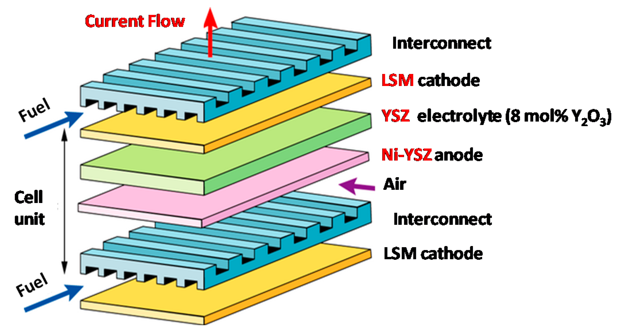
Planar SOFCs are operated at high temperatures (800–1000 °C) using a thin ceramic yttria-stabilized zirconia (YSZ) electrolyte and supporting Ni–YSZ anode layers [7,8,9,10]. YSZ has a 9.2 × 10⁻⁶/K thermal expansion coefficient, 1.8 W/m.k thermal conductivity, and melting temperature greater than 2780 °C. Lanthanum strontium manganite (LSM) or lanthanum strontium cobalt oxide (LSC) is used as a cathode layer. Stainless steel or ceramic interconnects is used for electric current routing. In a SOFC, a combination of a gaseous fuel (e.g., hydrogen or hydrocarbon fuels) and an oxidant gas (e.g., oxygen in the air) goes through electrodes and the reaction occurs on the anode and cathode, respectively. The actively charged carrier species go through an ion conducting electrolyte to generate an electronic current. A high density of YSZ is required in order to physically separate the gaseous fuel from oxygen to efficiently produce electricity.
Figure 1 gives a schematic drawing for a typical SOFC. Table 1 shows the design specifications of the SOFC for each layer. Once a cell is made and tested, the process is repeated to make the next cell to stack on the previous cell. The cathode (LSM), electrolyte (YSZ), or anode (Ni–YSZ) can be used as a supporting substrate in a three layer cell unit. In our case, we will focus on an anode supported SOFC.
3. Results and Discussion
3.1. Fabrication of Multi-Layer and Multi-Material Structures
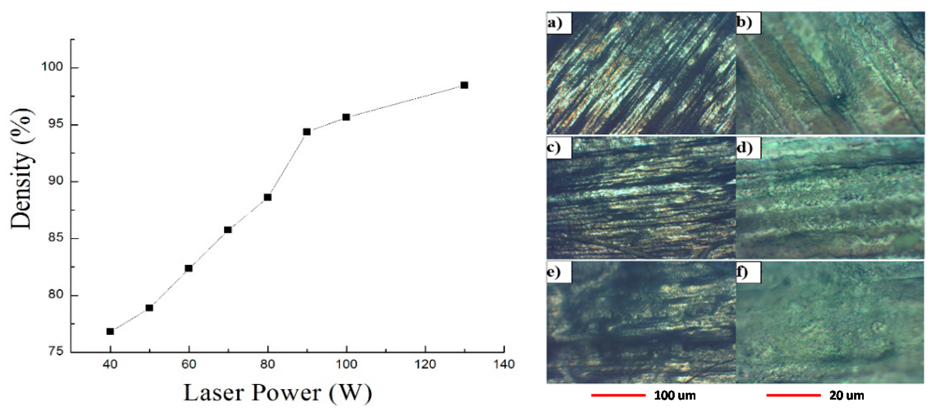
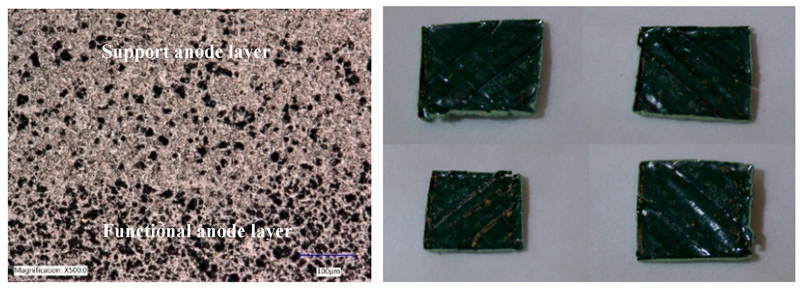
The Ni–YSZ supporting layer was first made with the LAM. Similar to YSZ LAM [11], the process window is small and a perfect match between the laser power and scan speed is critical. The feasibility of melting Ni–YSZ powders was successfully demonstrated with 80 MHz PRR femtosecond laser AM and without mixing any binders with the Ni–YSZ powders. Figure 2 (left) shows the experimental result of porosity (or relative density) as a function of laser power at a fixed scan speed of 300 mm/s. A high density of Ni–YSZ can be achieved at 130 W laser power and 300 mm/s scan speed. Lower density (high porosity, specifications of the Ni–YSZ anode are in Table 1) can be achieved by either increasing the scan speed to 500 mm/s or reducing the laser power. Figure 2 (right) shows the microscopic photos of the melted Ni–YSZ layers under various scan speed conditions at a fixed power of 130 W. The results show that high density Ni–YSZ had a better surface smoothness (with much clearer image) than the low density Ni–YSZ. Moreover, we also demonstrated that it was possible to control the laser power (Figure 2) to obtain a support layer and functional layer in one process. Figure 3 (left) shows an example with the combined functional anode layer and support anode layer. It has 35 to 40 vol% of Ni from Energy Dispersed X-ray spectroscopy (EDX) measurement. Figure 3 (right) are examples of anode samples with excellent uniformity and repeatability. These findings lay a solid foundation for the next LAM process of YSZ, the electrolyte layer.
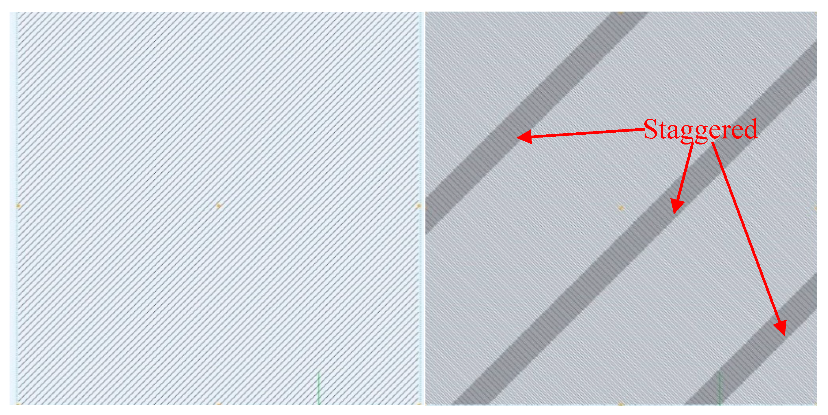
Second, a thin layer of YSZ, either in powder or ink, was spread on top of the Ni–YSZ anode support substrate and processed with the laser. Both can be melted and bonded on top of the anode surface, but the ink type of YSZ provides better uniformity. The scan patterning and hatching space play critical roles in the melting of YSZ on the Ni–YSZ anode. Two patterning types were systematically studied as shown in Figure 4, and the staggering pattern was better than the line pattern, with less thermally induced peeling off. YSZ was strongly bonded on Ni–YSZ. The YSZ layer was fabricated from 10 to 50 µm in thickness.
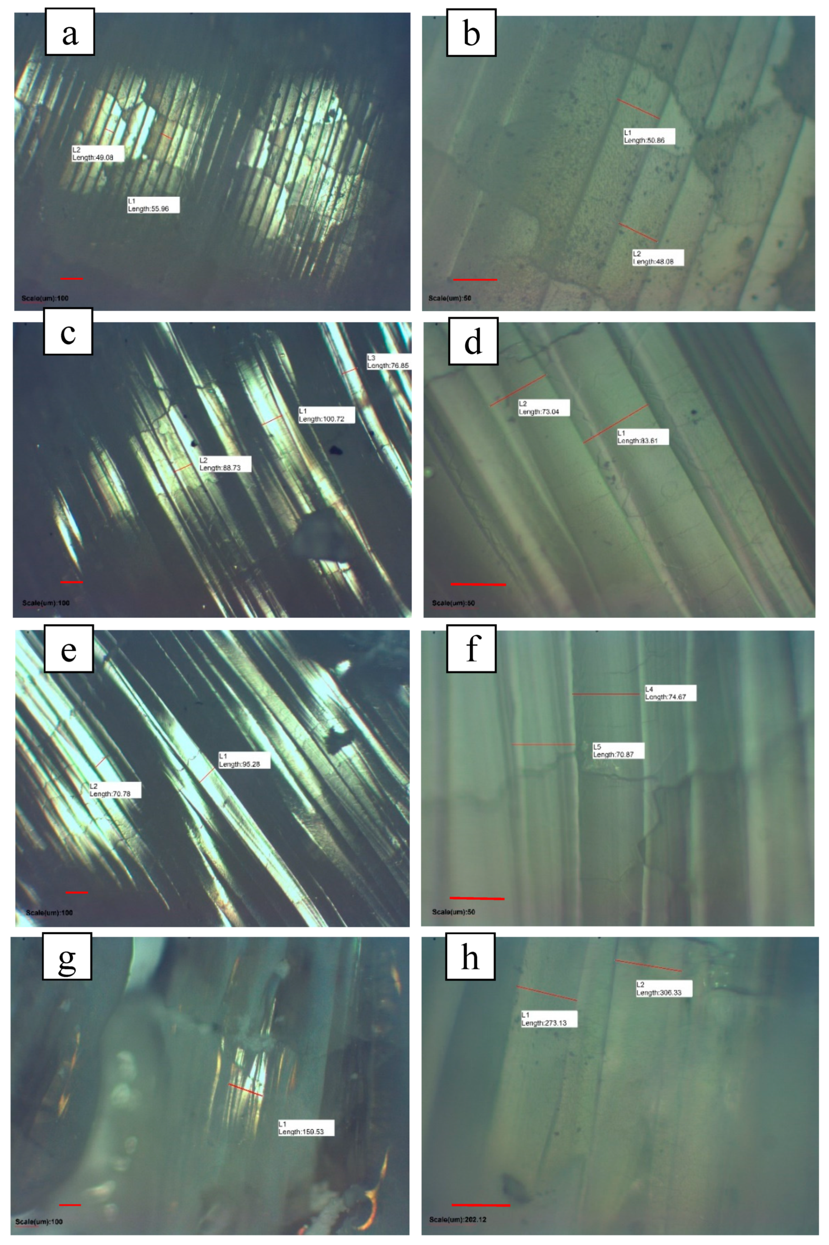
The melting effect of YSZ on Ni–YSZ as a function of hatching space was investigated and summarized in Figure 5. Figure 5a,b show the YSZ layers printed on the Ni–YSZ anode substrates with a hatching space of 15 μm, scanning speed of 80 mm/s, and on-target power of 78 W. Figure 5c,d show the results with hatching space of 20 μm, scanning speed of 100 mm/s and on-target power of 78 W. Figure 5e,f show the results with a hatching space of 20 μm, scanning speed of 80 mm/s, and target power of 78 W. Figure 5g,h show the results with a hatching space of 25 μm, scanning speed of 100 mm/s, and target power of 78 W. Images on the right column (b, d, f, h) differ only in the magnifying scale from their counterparts on the left column (a, c, e, g).
When the hatching space is too small, continuous ripple lines in the narrow space can be found. This results in more cracks propagating in the cross direction. Consequently, the porosity is large (as shown in Figure 5a,b). When the hatching space is too large, melted lines cannot be formed continuously, resulting in unmelt regions and fractured structure with large porosity (as shown in Figure 5g,h). At the hatching space of 20 μm, large uniformly melted regions with less cracks were found, as shown in Figure 5c–f. After the YSZ electrolyte layer was printed on the anode substrate, a thin layer of LSM (ink type) was spread on the YSZ layer and melted to serve as the cathode of the SOFC.
3.2. Three-Layered Cell Testing and Analysis
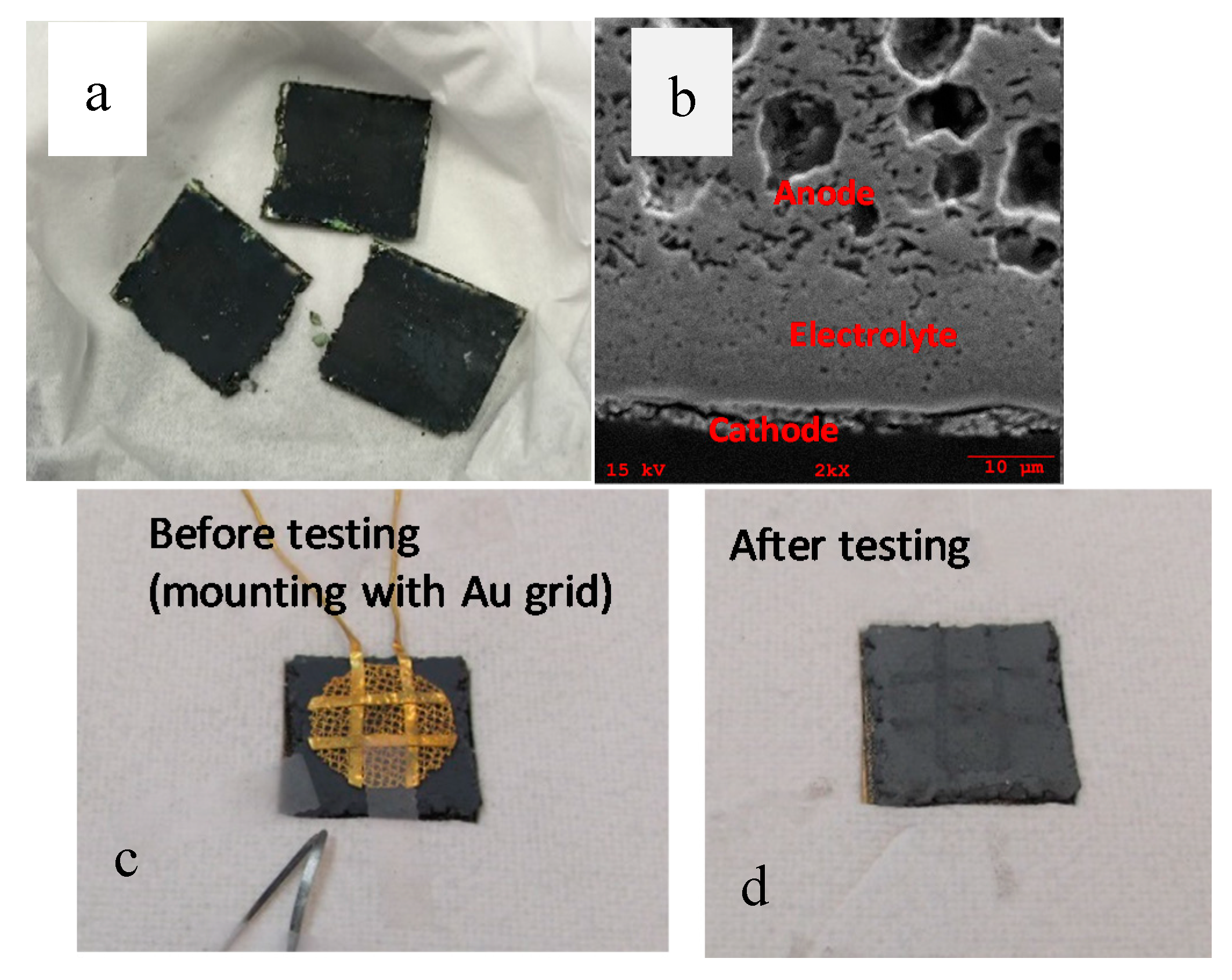
Figure 6a is a photo of the SOFC cells made from the same batch. Consistent and uniform three layered cells were made in our laboratories with up to a 30 × 30 mm active area. Figure 6b shows that the high strength of Ni–YSZ supporting anode can be achieved with controlled porosity at properly adjusted laser power and scan speed.
We have developed a process to control the laser power, scan speed, and scan patterning to obtain complete cell unit fabrication (anode, electrolyte, and cathode). Over 50% yield of complete SOFC cells was achieved from the anode substrates. The boundary and porosity were well controlled to achieve desired values as described in Table 1. A complete SOFC cell was sent to a third party (Fiaxell, Lausanne, Switzerland) for performance tests including polarization (I-V) curve and electro impedance spectroscopy (EIS). Figure 6c,d show the cell before and after the performance tests. Of note, since there is no interconnect integrated with the cell sample, it is a challenge for the Au grid attached to the cell to have a perfect contact. This may impact the final results. However, the purpose of this publication is to demonstrate that the basic three-layered structure (anode, electrolyte, and cathode) made with LAM can generate a current.
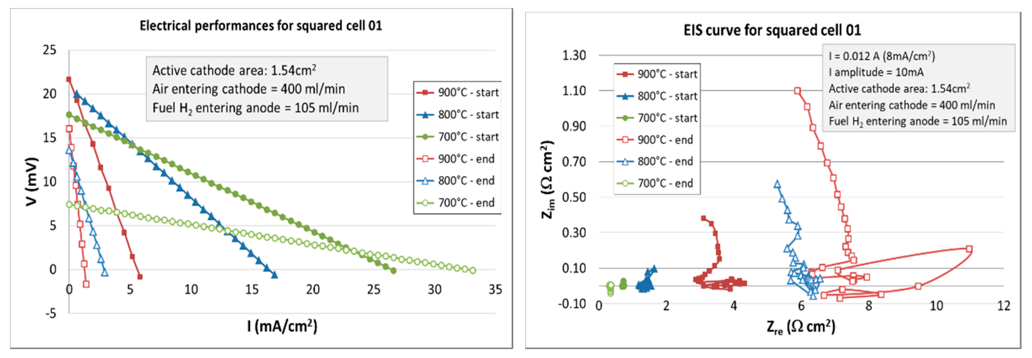
The testing results are shown in Figure 7. The cell sample was functional and an electrical current was generated. Two measurements were implemented to reflect the time dependent performance. Data with solid markers were taken right after injecting the H2 into the cell. The cell was then kept in a protective atmosphere (200 mL/min of 92%N2 + 8%H2) overnight. Data with open markers were taken after 18 h in 92%N2 + 8%H2, followed by the injection of H2. Three temperatures (700 °C, 800 °C, and 900 °C) were sequentially tested. The resistance of cells was found to be much higher than the SOFC made by conventional approaches such as cold spray. The higher resistance causes a lower voltage and lower current at the same time. Based on our current LAM process, the high resistance may be caused by the thickness control of the YSZ electrolyte, with the thickness being either too large or non-uniform. The second possibility is the YSZ electrolyte layer does not connect well with both the Ni–YSZ anode and LSM cathode layer (disconnection). The third issue may come from the Au grid attachment in testing. The Au grid might not be in physical contact with the testing cell during the 18 h testing period. All these issues are related to the uniformity control of the LAM process over the entire SOFC area, especially the surface roughness of the Ni–YSZ anode and thin layer printing uniformity of the YSZ electrolyte. We are currently working to improve the control process. In future activities, a full temperature range, temperature cycling, and damp heat will be used to test its reliability and endurance. A model related to the LAM process will be built to analyze its failure mode and mechanism.
4. Conclusions
For the first time, a three layered structure, as a basic cell unit of SOFC, was built and demonstrated via laser additive manufacturing. The processed multi-layer structure was examined and characterized, and a basic cell sample was tested on polarization I-V and EIS curves. It shows that the density and porosity can be well controlled during the LAM process, and that the basic SOFC cell sample functions. We believe that once the interface strength and uniformity of the YSZ electrolyte thickness, reduction of the Ni–YSZ surface roughness, and the LAM integration of the interconnect are improved, there will be great potential for many applications.
Author Contributions
Conceptualization, J.L. and S.B.; methodology, S.B.; formal analysis, S.B. and J.L.; investigation, S.B. and J.L.; writing—original draft preparation, S.B.; writing—review and editing, J.L.; supervision, J.L.; project administration, J.L.; funding acquisition, J.L. All authors have read and agree to the published version of the manuscript.
Funding
This research was funded by the Department of Energy (DOE) Small Business Innovation Research (SBIR) SBIR DE-SC0015199.
Acknowledgments
This research was funded by the Department of Energy (DOE) Small Business Innovation Research (SBIR) SBIR DE-SC0015199. Special thanks go to Patcharin Burke for her guidance and support.
Conflicts of Interest
The authors declare no conflicts of interest.
References
- Kamath, C.; El-dasher, B.; Gallegos, G.F.; Gallegos, W.; King, W.E.; Sisto, A. Density of additively-manufactured, 316L SS parts using laser powder-bed fusion at powers up to 400 W. Int. J. Adv. Manuf. Technol. 2014, 74, 65–78. [Google Scholar] [CrossRef] [Green Version]
- Abe, F.; Osakada, K.; Shiomi, M.; Uematsu, K.; Matsumoto, M. The manufacturing of hard tools from metallic powders by selective laser melting. J. Mater. Process. Technol. 2001, 111, 210–213. [Google Scholar] [CrossRef]
- Bai, S.; Yang, L.; Liu, J. Manipulation of Microstructure in Laser Additive Manufacturing. Appl. Phys. A 2016, 122, 495. [Google Scholar] [CrossRef]
- Nie, B.; Huang, H.; Bai, S.; Liu, J. Femtosecond laser melting and resolidifying of high-temperature powder materials. Appl. Phys. A 2015, 118, 37–41. [Google Scholar] [CrossRef]
- Nie, B.; Yang, L.; Huang, H.; Bai, S.; Wan, P.; Liu, J. Femtosecond laser additive manufacturing of iron and tungsten parts. Appl. Phys. A 2015, 119, 1075–1080. [Google Scholar] [CrossRef]
- Fulcher, B. Effects of Laser Parameter Variation and Thermal Processing on Mechanical Properties and Microstructure of Laser-Melted Inconel 718. In Proceedings of the Additive Manufacturing with Powder Metallurgy Conference, Orlando, FL, USA, 19–20 May 2014; p. 146. [Google Scholar]
- Huang, W.L.; Zhu, Q.; Xie, Z. Gel-cast anode substrates for solid oxide fuel cells. J. Power Sour. 2006, 162, 464–468. [Google Scholar] [CrossRef]
- Sammes, N.M.; Du, Y.; Bove, R. Design and fabrication of a100W anode supported micro-tubular SOFC stack. J. Power Sour. 2005, 145, 428–434. [Google Scholar] [CrossRef]
- Lawlor, V. Review of the micro-tubular solid oxide fuel cell (PartII: Cell design issues and research activities). J. Power Sour. 2013, 240, 421–441. [Google Scholar] [CrossRef]
- Ding, J.; Liu, J.; Yuan, W.; Zhang, Y. Slip casting combined with colloidal spray coating in fabrication of tubular anode-supported solid oxide fuel cells. J Eur. Ceram. Soc. 2008, 28, 3113–3117. [Google Scholar] [CrossRef]
- Liu, J.; Bai, S. Femtosecond laser additive manufacturing of YSZ. Appl. Phys. A 2017, 123, 293. [Google Scholar] [CrossRef]
Figure 1.
Solid oxide fuel cell (SOFC) design architecture. A single cell unit include cathode (LSM), electrolyte (YSZ), and anode (Ni–YSZ). In this paper, the anode layer is the supporting substrate.
Figure 1.
Solid oxide fuel cell (SOFC) design architecture. A single cell unit include cathode (LSM), electrolyte (YSZ), and anode (Ni–YSZ). In this paper, the anode layer is the supporting substrate.

Figure 2.
(Left) Density as a function of laser power at a scan speed of 300 mm/s. (Right) Microscopic images of melted layer with a target power of 130 W, hatching space of 30 μm, scanning speed at 300 mm/s (a,b), 400 mm/s (c,d), and 500 mm/s (e,f). (Right) column images (b,d,f) are magnified images of the left column (a,c,e).

Figure 3.
(Left) Cross-section scanning electromagnetic (SEM) image of the interface between the functional layer and support layer of the anode. (Right) Ni–YSZ anode samples (the largest size was 30 × 30 mm).
Figure 3.
(Left) Cross-section scanning electromagnetic (SEM) image of the interface between the functional layer and support layer of the anode. (Right) Ni–YSZ anode samples (the largest size was 30 × 30 mm).

Figure 4.
Types of scan patterning of LAM process for YSZ on Ni–YSZ. Staggered pattern (Right) shows less peel-off issues during the AM process than the line pattern (Left).
Figure 4.
Types of scan patterning of LAM process for YSZ on Ni–YSZ. Staggered pattern (Right) shows less peel-off issues during the AM process than the line pattern (Left).

Figure 5.
Microscopic images (different scales) of the YSZ layer printed on the Ni–YSZ anode substrates. (a,b) Hatching space of 15 μm, scanning speed of 80 mm/s, and target power of 78 W; (c,d) hatching space of 20 μm, scanning speed of 100 mm/s, and target power of 78 W. (e,f) Hatching space of 20 μm, scanning speed of 80 mm/s, and target power of 78 W. (g,h) Hatching space of 25 μm, scanning speed of 100 mm/s, and target power of 78 W.

Figure 6.
(a) Complete three layered cell samples (30 × 30 mm); (b) cross-section SEM image of the interfaces for a complete cell sample; (c) a cell sample is mounted with a Au grid for testing I-V curve and EIS; (d) the cell sample after testing.
Figure 6.
(a) Complete three layered cell samples (30 × 30 mm); (b) cross-section SEM image of the interfaces for a complete cell sample; (c) a cell sample is mounted with a Au grid for testing I-V curve and EIS; (d) the cell sample after testing.

Figure 7.
Polarization (I-V) curve and electro impedance spectroscopy (EIS) test curve for a cell sample.
Figure 7.
Polarization (I-V) curve and electro impedance spectroscopy (EIS) test curve for a cell sample.


Table 1.
Solid oxide fuel cell (SOFC) structure specifications.
| Component | Material | Thickness | Porosity |
|---|---|---|---|
| Anode | Ni–YSZ | 0.3–0.6 mm | ~40% |
| Electrolyte | YSZ | 5–10 µm | <5% |
| Cathode | Conducting ceramic | 10–50 µm | ~30% |
© 2020 by the authors. Licensee MDPI, Basel, Switzerland. This article is an open access article distributed under the terms and conditions of the Creative Commons Attribution (CC BY) license (http://creativecommons.org/licenses/by/4.0/).
Share and Cite
MDPI and ACS Style
Bai, S.; Liu, J. Femtosecond Laser Additive Manufacturing of Multi-Material Layered Structures. Appl. Sci. 2020, 10, 979. https://0-doi-org.brum.beds.ac.uk/10.3390/app10030979
AMA Style
Bai S, Liu J. Femtosecond Laser Additive Manufacturing of Multi-Material Layered Structures. Applied Sciences. 2020; 10(3):979. https://0-doi-org.brum.beds.ac.uk/10.3390/app10030979
Chicago/Turabian StyleBai, Shuang, and Jian Liu. 2020. "Femtosecond Laser Additive Manufacturing of Multi-Material Layered Structures" Applied Sciences 10, no. 3: 979. https://0-doi-org.brum.beds.ac.uk/10.3390/app10030979
Note that from the first issue of 2016, this journal uses article numbers instead of page numbers. See further details here.