Advances in Imaging Diagnostics for Spray and Particle Research in High-Speed Flows

Artium Technologies, 470 Lakeside Dr., Sunnyvale, CA 94085, USA
*
Author to whom correspondence should be addressed.
Appl. Sci. 2020, 10(4), 1450; https://0-doi-org.brum.beds.ac.uk/10.3390/app10041450
Submission received: 22 January 2020
/
Revised: 12 February 2020
/
Accepted: 14 February 2020
/
Published: 21 February 2020
(This article belongs to the Special Issue Progress in Spray Science and Technology)
Abstract
:Measurements of high-pressure sprays and particle fields in high-speed flows have been very challenging for the existing instrumentation. Deformed drops or solid particles significantly limit the range of experimental methods that can be applied for detailed, quantitative measurements. We developed advanced microscope imaging equipment and diagnostic methods to characterize fast-moving droplets or particles. We designed illumination systems based on high-power light-emitting diode (LED) and incoherent laser devices capable of short, intense light pulses. We compared their characteristics and performance separately, as well as their interaction within a complete line-of-sight microscope imaging system. The optical design of the microscope setup was optimized via ray tracing simulations showing high energy losses for LED illumination compared to laser radiation, as confirmed experimentally. The energy transmission measurements provided guidance about the pulse energy density necessary to maximize camera response and signal-to-noise ratio. Characterization testing supported that both illumination systems are valid options for microscopy applications, with an advantage to LED for image quality and resolution performance, but a strong limitation to distance, where the multi-beam laser system demonstrated its superiority.
1. Inroduction
Sprays are routinely used in our daily lives; from medical to industrial, as well as transportation technologies, the applications are countless [1]. The wide range of applications means an equally large spectrum of spray and droplet field requirements and properties. High-velocity sprays, such as those found in in thermal engines [2] or thermal spray technologies [3], have very specific requirements to make them as effective as possible. Beyond sprays, high-speed multi-phase or particle flows are also used in a vast number of applications, from explosion residues [4] to weather-induced ice crystals [5]. In many of the aforementioned applications, parameters such as drop size, velocity, concentration, and many more need to be tightly controlled to ensure that the spray or particle field present the optimal properties.
The study and characterization of sprays alongside droplets and particle fields have been benefiting from advanced diagnostics for decades, and the technological advancements consistently and regularly push the capabilities [6,7]. Diagnostic methods represent the tools researchers have at their disposal to study sprays and particle fields. Non-intrusive diagnostics are highly desirable in most spray and particle field characterization efforts, but their implementation may require specific developments to be appropriate for the required information to be extracted, or to simply fit within the experimental constraints. Advanced, non-intrusive diagnostics are needed today to uncover important aspects about sprays and particle fields, especially in high-speed flows.
Optical measurement tools in general, and more specifically laser-based diagnostics, have contributed to significant discoveries in the present field and many others over the last decades. There is an extensive list of methods employing laser light to investigate sprays and particle fields; they can be point-source [8,9], planar [10,11], or three-dimensional [12,13]. These different methods focus on one aspect or another, and come with their respective strengths and weaknesses, making them suitable to a range of applications and conditions. Half of the methods listed above rely on the Mie scattering theory, which is valid for spherical particles (drops), but fails in the presence of non-spherical particles (solid, ice, etc.) [14].
Complimentary to other non-intrusive methods, such as laser diagnostics, imaging has been widely applied to analyze or investigate sprays and particles fields. The two-dimensional aspect of the data enables imaging to cover a wide range of applications, including the characterization of solid and non-spherical particles, where laser diagnostic methods relying on the Mie scattering theory are no longer appropriate [15]. Driven by machine vision, digital cameras now feature megapixel sensors which offer comparable light collection and conversion efficiency compared to expectedly superior scientific equipment. State-of-the-art streaming cameras are nearly matching the pixel throughput of dedicated high-speed cameras, whereas they are smaller, easier to implement, and substantially cheaper. Another advantage of machine vision cameras for microscope imaging applications compared to advanced high-speed cameras is the pixel dimension. High-throughput sensors are available in machine vision with small pixels in comparison to high-speed cameras. Although large pixels are necessary to collect the amount of light to optimize dynamic range, they are detrimental to microscopy applications, where it becomes difficult to match the microscope objective with the pixel characteristics of the sensor to optimize the imaging systems optical resolution [16]. The illumination side has also benefited from improvements in semiconductor technology in recent years, with the significant progress made by light-emitting diode (LED) emitters. Widely used today for industrial lighting applications as a result of significant improvements in luminous power output and efficiency, LEDs have shown good performance with respect to high-speed operation as well [17].
In this work, we investigated the characteristics and performance of a long-distance microscope imaging system optimized for quantification of droplets and particle fields in high-speed flows. We thoroughly characterized illumination systems based on light-emitting diode (LED) and a laser technology newly introduced for imaging applications: the vertical-cavity surface-emitting laser (VCSEL). The illumination systems were designed to generate short pulses of uniform light over the small probe volume created by the camera and associated long-distance microscope objective. Relevant characteristics of the high-resolution, high-throughput machine-vision camera were also measured, to ensure optimal image quality and signal integrity. The energy transmission characteristics of the illumination systems and their relationship to the image acquired by the camera were measured and analyzed, providing estimates of the energy delivered by the illumination systems to the object and image planes. Such information is necessary to understand how much energy is needed to optimize dynamic range and maximize signal-to-noise ratio of a digital imaging system. Laboratory testing was undertaken to characterize the imaging system with both illuminations devices, focusing on parameters relevant to microscopy measurements of droplet and particles in high-speed flows. We finally performed droplet size measurements on a droplet field produced by a commercial air-operated spray system, eventually demonstrating the high performance of the system in that regard.
The present manuscript follows the organization given hereafter. The experimental apparatus is presented in Section 2, including a description of the various components of the imaging and illumination systems. Section 3 aims at characterizing the LED and VCSEL illumination systems and evaluate their performance in the context of line-of-sight microscopy for high-speed operation. In Section 4, the imaging system is characterized, again comparing the two illumination devices, and including measurement-based correlations between photonic energy and digital levels. This section also reports the sample droplet sizing experiments with the two illumination systems. Section 5 summarizes the findings and concludes this work.
2. Microscope Imaging Apparatus
A bright-field digital microscope imaging system is composed of several elements, including an illumination source and a digital camera equipped with a microscope objective. These elements need to be carefully selected or designed, as well as thoroughly characterized to ensure optimal performance. Balancing optical resolution, magnification, working distance, and field of view, for example, is a difficult task, with multiple parameters available to optimize the system according to the specific requirements of the imaging experiments. For the purpose of this work, we proposed a configuration with a working distance above 100 mm, and a digital resolution in the vicinity of 2.5 /pix. The imaging system is optimized to capture high-quality images of particles ranging in diameter between below 10 to 1 mm or larger, in flows at speeds up to 100 m/s. With these requirements in mind, the system’s first priority was image quality, which implies identifying the optimal balance between optical and digital resolution, as well as making sure the particles are captured no apparent motion blurring deterioration.
2.1. Ultra-Fast Illumination Solutions
The light source is a critical component of a microscope-based imaging system; every aspect of the light characteristics bears importance when the system needs to be optimized. The first parameter of a microscope imaging system is its effective optical resolution. Though generally correlated, magnification alone does not tell much about the performance of a system. Looking at resolution in optical microscopy from a fundamental standpoint, we realize it is limited by diffraction. A properly configured and set up microscope is said to be diffraction-limited, which can be expressed by criteria proposed by Abbe or Rayleigh [18]. They relate the illumination wavelength and numerical aperture of the receiving optics to estimate the diffraction-limited resolution of a system, demonstrating that shorter wavelengths and high numerical apertures are beneficial to optical resolution.
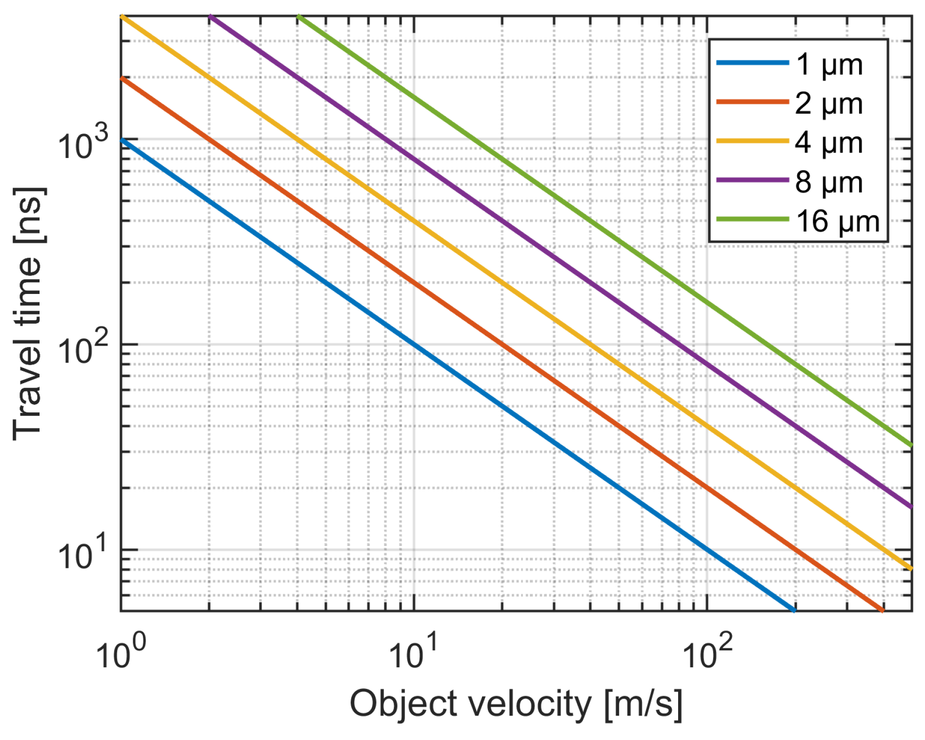
One important aspect of particle characterization in high-speed flow is the negative effect of motion blurring. Motion blurring is the result of the displacement of the object under study during the imaging system’s exposure, with the image of the object appearing blurred or smeared. Objects moving at high speeds require short exposures to be captured without any apparent exposure-related blur. The situation becomes even more challenging under microscopy application, where typical camera shutter times, even scientific equipment, are much longer than what is needed to capture the object without motion blur. In this case, high-power light pulses are used to illuminate the scene for a short duration, with the camera sensor exposed for a longer time period. Assuming that the amount of background light integrated by the sensor over the camera exposure is negligible compared to the amount of energy delivered by the short light pulse, the pulse width becomes the effective exposure time. Figure 1 shows the travel time as function of object velocity for select linear displacements from 1 to 16 . This plot provides a simplistic perspective on the exposure or pulse duration requirements to limit or avoid motion blur for a range of length-scales, which can be interpreted as the system’s spatial resolution.
Although straightforward in nature, the results of Figure 1 highlight the stringent pulse width requirements when measuring small particles at high speeds. For instance, particles smaller than 10 in 100-m/s flow must be illuminated by a sub-100 ns pulse not to be significantly affected by motion blurring when imaged by a microscope setup. Correction methods have been proposed to compensate the effects of motion blurring [19,20]. Although these methods are successful when applied to known objects or displacement, this is not necessarily the case in high-speed flow. As such, and based on the requirements listed above, we decided to set the illumination duration to approximately 50 ns to ensure that particles would be imaged with no apparent motion blurring.
The output radiation distribution is another important aspect of the illumination system, especially when dealing with high-speed flows and short pulse duration. The scene needs to be properly illuminated, as seen from the camera perspective. This means that the integrated photonic intensity over an imaged pixel area between the object and image planes needs to be sufficient to maximize the sensor’s dynamic range. The intensity at the probe volume is therefore paramount, and the characteristics of the light source may or may not present the right output radiation properties to be transmitted over large distances.
There are a number of light sources to can be considered for the present applications, and they all present strengths and weaknesses. After designing, testing, and evaluating several solutions, we found that both light-emitting diodes (LEDs) and vertical-cavity surface-emitting lasers (VCSELs) presented adequate characteristics to answer the specific requirements listed above. LEDs have seen a growing interest over the last decade for illumination and even electromagnetic signal transmission. New designs are highly efficient and can produce illumination power from a relatively small emitting area. LEDs are available in various wavelengths, from ultraviolet to infrared, and of course white, with the addition of a phosphor. LEDs present definitive advantages for illumination with respect to background uniformity, and the absence of speckle and diffraction patterns that plagued laser illumination, mainly due to the limited monochromatic and coherent properties of LED emitters, in general. The low coherence and large emitting area, however, have a negative impact on the property of the high-dispersion radiation to be shaped and collimated, and thus transmitted over long distances.
Although LEDs are the most appropriate choice for most applications, long working distances limit their use. We therefore developed another illumination source to use in arrangements where LEDs are no longer applicable. Employing high-power versions of vertical-cavity surface-emitting lasers (VCSELs), a technology developed mainly for telecommunication, the high bandwidth and speckle-free output radiation is more in line with the needs of line-of-sight microscopy than other laser technologies. We have combined up to six (or more) VCSEL devices into a multi-beam illumination arrangement [21]. The output radiation in this configuration presents further reduced coherence and a wider wavelength distribution, by mixing the wavefronts coming from different laser devices. The multi-beam arrangement has also been observed to behave in a diffuse manner, which helps mitigate depth-of-field effects and corruption of images due to larger particles passing through the illumination beams outside of the object plane.
2.1.1. High-Power Light-Emitting Diode Illumination Source
We have developed various high-current electronics for our LED system, increasing or tuning their performance with each generation. The latest driver was developed for a quad-channel multi-die LED emitter, which demonstrated exceptional bandwidth at very high radiation power. This four-channel driver can generate short pulses at current levels above 220 A. It demonstrated extreme stability, short pulse capability below 10 ns, and repetition rates well above 5 MHz, a major improvement compared to all commercially available systems. In this work, we coupled the driver with a custom-made royal blue, quad-channel, multi-die LED emitter (custom LEDengin LZP). The customization of this LED emitter includes the selected wavelength of the emission spectrum (centered at 457 nm, with a 22-nm bandwidth), as well as the replacement of the LED glass dome for a flat glass window, which contributes to the simplicity and flexibility of the optical set-up to maximize light collection and transmission. Blue and UV LED emitters generally present the highest flux of all LED chips; they rely on a gallium nitride (GaN) semiconductor to form a p–n junction by silicon and magnesium doping, and convert the electric energy into photons of short wavelength, due to the high energy bandgap of GaN. Indium nitride (InN) is typically added to GaN to change the energy bandgap and tune the dominant radiation wavelength of the LED.
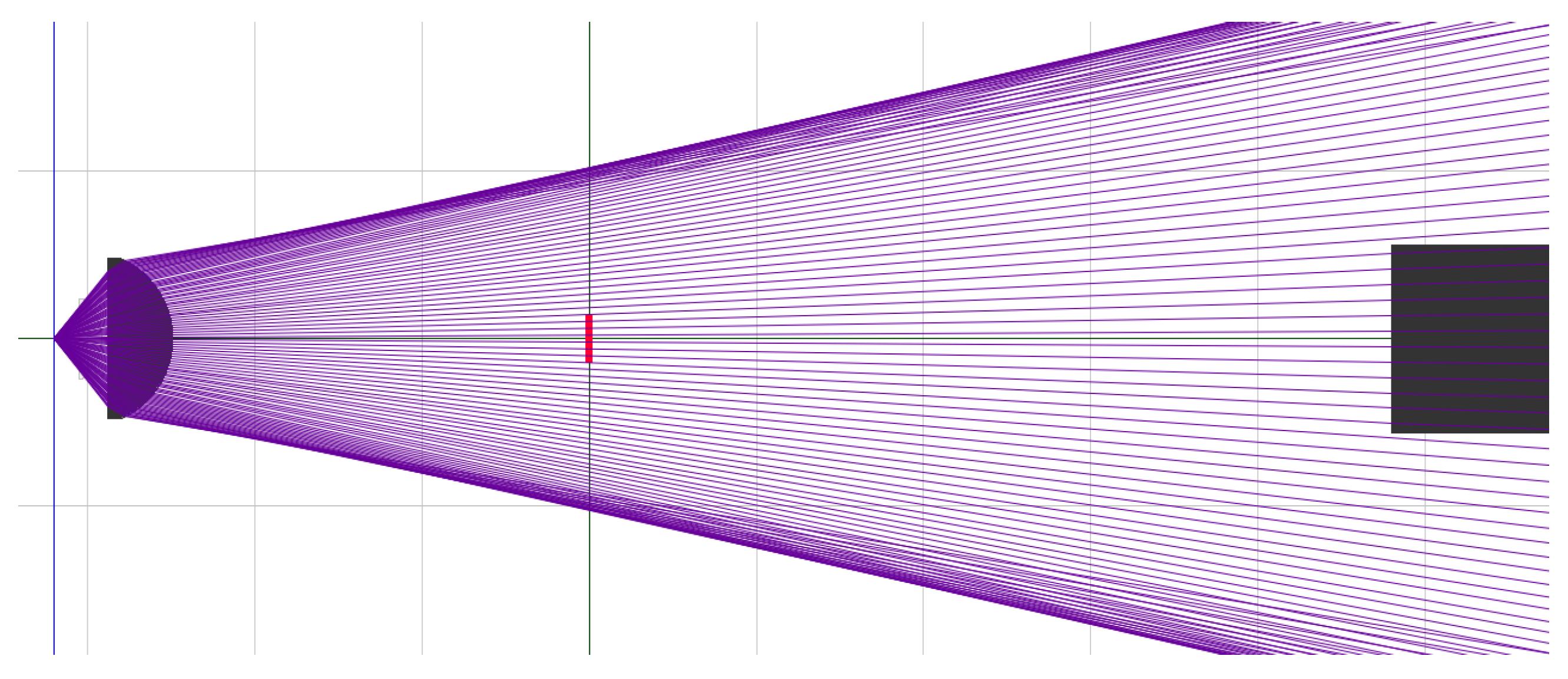
The high dispersion of typical LED output radiation (120 for the emitter used in this work) results in rapidly decreasing energy density on and off axis with distance. Specific optics need to be used to collect and transmit the LED output light with the minimum amount of energy loss. To keep the configuration simple in this work, we used a single 16-mm focal length aspheric condenser lens located just under 10 mm away from the LED emitter’s glass window. Figure 2 presents a ray tracing simulation of the optical arrangement, with the LED emitter located on the far left of the diagram, and the light rays represented in purple color. The measurement volume is represented in red, at 80 mm from the LED emitter, with the middle of the measurement volume corresponding to the object plane. The condenser lens is shown in dark gray and the effective collection space of the long-distance microscope objective is shown by a dark gray rectangle.
The ray tracing simulations of Figure 2 show the good behavior and coherence of the wavefront, as indicated by the unidirectional trajectories of the rays, which is important for line-of-sight imaging. This configuration represents a factor nine improvement over the bare LED emitter at this location, according to the ray tracing simulation results. Nevertheless, a large fraction of the LED output radiation does not illuminate the probe volume, with nearly over a 99% loss. These simple simulations do not account for the energy distribution of the LED emitter, but only represent the radiation over the full width at half maximum angle, per the LED specifications (120). More accurate energy figures are provided later in this manuscript along with a full characterization of the LED radiation output.
2.1.2. Multi-Beam Vertical-Cavity Surface-Emitting Diode Laser Array
To answer the needs for more efficient light transmission, we have developed VCSEL-based light sources as a means to achieve high quality illumination that is uniform and free of laser speckle [21]. The devices were originally developed for data communication and local-area networks and were designed to replace edge-emitting lasers. The lasers consist of layers of semiconductor material, which is grown on top of each other on a substrate. In the lasing medium of a VCSEL, the light oscillates perpendicular to the layers and exits through the top of the device. This laser technology offers a number of advantages over edge-emitting laser diodes, such as higher quality beam, practically easier implementation, and their ability to operate at relatively high temperatures, thus not requiring dedicated cooling. For aircraft icing applications, the laser may be in an environment close to the probe heaters so the temperature insensitivity is important. These lasers can deliver very high power per unit area reaching approximately 1200 . They emit a circular beam which can be shaped to have a Gaussian intensity distribution. This simplifies the optics needed for transforming the beam to a near top hat intensity distribution. High-power VCSEL devices combine hundreds or thousands of individual VCSEL sources.
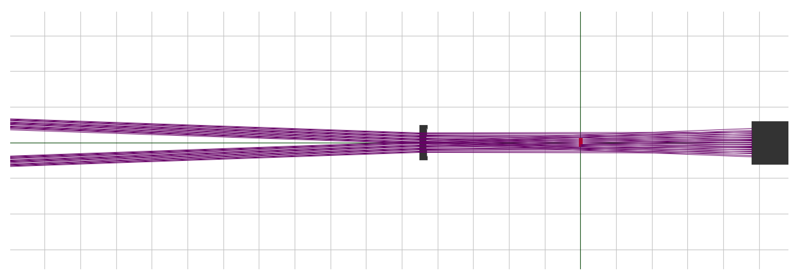
As mentioned above, beam quality is one of the many advantages of VCSEL technology compared to laser diodes. Beam divergence of bare VCSEL devices is approximately 20, which is substantially narrower than LEDs, providing a significant advantage for light transmission. For this research, we selected a VCSEL device (FLIR CWV-HP) equipped with integrated optics to control beam divergence and provide a near-Gaussian distribution with a dispersion angle on the order of 7. The relatively small emitting area and low divergence enable the beam output to be collimated for transmission over larger distances, a key advantage compared to LEDs, as stated above. We used 100 mm focal length plano-convex lenses to collect and nearly collimate the radiation coming from each VCSEL in the multi-beam assembly. The six beams are converged at a 2 angle, and merged by a plano-concave lens with a −200 mm focal length. This produces a circular distribution on the order of 10 mm in diameter at the object plane located 130 mm away from the plano-concave lens (represented in red), and 12 mm at the receiving optics’ effective front element (dark gray rectangle). The partial results of the ray tracing simulations carried out to optimize this optical arrangement is provided in Figure 3.
As suggested by the ray tracing simulations, the output of the VCSEL illumination system is a slightly diverging beam, which is fully collected by the receiving optics, as demonstrated by the dark gray rectangle on the right side of the diagram. Compared to the LED simulation results, the ray tracing diagram of Figure 3 indicates that over 20% of the laser radiation is illuminating the probe volume, compared to less than 1% for the LED system, despite the condenser lens. Note that the distances are much greater than for the LED system to achieve optimal illumination distribution with the VCSEL system. The length of the arrangement shown in Figure 3 is more than twice that of the LED-based arrangement, and it does not include another 150 mm necessary for proper VCSEL collimation. In total, the VCSEL-based illumination system is approximately 550 mm long to the object plane. Although the size of the optical arrangement for the illumination system may not be a problem in most applications, it must be considered when compactness is required.
As described above, VCSEL devices are based on laser diodes, and as such, their radiation is expected to be monochromatic. The VCSEL used in this study has a radiation wavelength centered at 860 nm, and features a spectral spread close to 1 nm. Such a narrow spectral range may be problematic for line-of-sight microscopy measurements, as it could produce interference patterns around the edges of objects. The multi-beam approach, with six independent laser units, serves to mitigate this condition. The near-infrared wavelength of the lasers may also be detrimental to resolution in microscopy as suggested by the theory with the wavelength relationship with the diffraction limit [18].
2.2. High-Resolution Digital Camera and Long-Distance Microscope Objective
Although there are many options to record high-quality images under the conditions relevant to this study, the advantage of high-performance machine vision cameras or streamers, compared to dedicated, state-of-the-art high-speed cameras was discussed in the introduction (c.f. Section 1). For this work, we used a customized high-resolution digital camera equipped with a 12 Mpix CMOS sensor (AMS CMV12000), or 4096 × 3072 pixels. The camera sensor features square, 5.5 pipelined global shutter pixels, for image-side sensor dimensions of 22.5 × 16.9 . The sensor counts 64 12-bit digitizers which can be operated at 8-, 10-, or 12-bit digital output, allowing the sensor to acquire at rates up to 330 frames per second in full-frame, 8-bit mode. The camera is connected to the computer system via fiber optics operating at 25 Gbit/s (SFP28 protocol), and streams the data directly to either the computer memory (RAM) or a dedicated high-speed storage system. As a result of limitations in camera front end electronics, the imaging system can effectively records full-frame images at acquisition rates up to 188 frames per second in 8-bit digital output mode, equivalent to 18.9 Gbit/s. A more practical metric to assess camera readout performance is the effective pixel throughput , which simply multiplies the selected pixel count and acquisition frame rate combination [16]:
where is the total number of pixels at which the camera can sustain the associated frame rate. The total number of pixels is calculated by summing all pixels or multiplying the horizontal () and vertical () sensor pixel counts. Under the present camera settings (full-frame, 8-bit digitization), the maximum effective pixel throughput is 2.37 Gpix/s. Such digital throughput approaches the performance of dedicated high-speed streaming cameras, or even that of entry-level high-speed cameras. Direct comparison is difficult, however, because high-speed cameras generally employ lower pixel count sensors than the 12 Mpix device used in this study. Although the exposure time is set by the LED or laser pulse, the camera was exposed for 100 during the experiments. Such a short exposure time ensures the minimal amount of flare from the environment, but also minimizes the dark current and other exposure-related noises to be significant.
The camera and illumination systems were synchronized by the camera frame output signal. This signal was used as input trigger to a 120 MHz arbitrary waveform generator configured in pulse mode. The delay between the frame acquisition output signal and the electrical pulse signal for the illumination was set to 1 , and camera shutter and illumination jitter was below 5 ns, which is insignificant compared to the 100 camera exposure time. The operating rate of the system was effectively determined by the camera acquisition frequency; which was set to 100 Hz for all the experiments reported in this manuscript.
The long-distance microscope lens attached to the camera works in conjunction with the camera’s sensor to provide the appropriate resolution at the object plane. We tested several state-of-the-art microscope objectives matching the requirements set for this work, and selected the Infinity K2-DistaMax because it offered the highest optical performance, certainly a result of the large optics used (2 diameter). The microscope lens was equipped with the CF-3 objective, and set at 120 mm from the object plane, providing a magnification factor of 2.2×. Note that the object plane moved away from the microscope objective by 3.7 mm when VCSEL illumination was used. This is expected given that the microscope objective does not feature chromatic correction. The measured digital resolution at the object plane was 2.5 , which matches the intended specifications for this set-up. As such, the field of view at the object plane was 10.2 × 7.7 . With an effective front element diameter of 38 mm, the numerical aperture of the microscope objective was 0.156 under the present configuration, which equates to a diffraction-limited resolution of 1.77 for the LED illumination, and 3.35 for the VCSEL, based on the Rayleigh criterion.
3. Illumination Systems’ Performance Comparisons
Under high-speed particle field conditions, it is imperative for the illumination system to produce short light pulses to capture the particles without the collateral motion blurring effects. Beyond short pulse performance, another critical aspect is light transmission efficiency, such that the highest fraction of the output radiation may be used to illuminate the scene and later collected by the imaging system’s receiving optics. Although lasers are known to offer near ideal output radiation characteristics to that end, it is more complicated for LED light output to be collimated, due to the non-coherent aspect of the radiation, in addition to the generally large emitting area. The present section investigates the different aspects of VCSEL and LED radiation relevant to microscopy applications under high-speed flow conditions.
3.1. Bandwidth and Short Pulse Capabilities
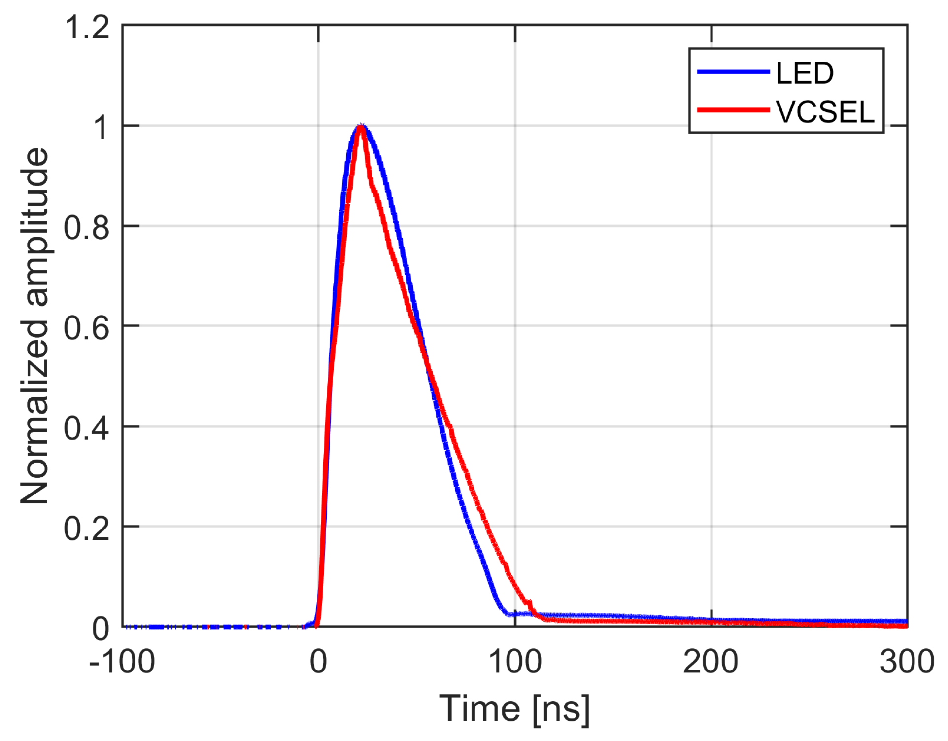
At the flow speed and imaging system’s resolution, the objective for the illumination sources is to generate light pulses of approximately 50 ns duration carrying the maximum amount of energy to the probe volume and later collected by the receiving optics. We used a high-speed photo-detector to measure the temporal pulse profile emitted by the VCSEL and LED systems, and recorded the signal with a computer-based 200 MHz oscilloscope. The photo-detector rise and fall times are on the order of 1.5 ns, which is sufficient to track the ramp up and decay of the light pulses. The results of the pulse profiles for a 50 ns duration for both VCSEL and LED-based illumination sources are presented in Figure 4.
The profiles of Figure 4 show that both the VCSEL and the LED systems offer high-speed capabilities when driven by the respective electronics developed in our laboratories. As expected, the two light pulses coincide in duration at the half intensity mark, both producing 50 ns light pulses, based on the full width at half maximum measurement. Surprisingly, and despite the differences being minor, the LED system’s bandwidth appears to be superior to that of the VCSEL illumination system. Both systems present fast ramp-up profiles of approximately 10 ns, but the decay is noticeably faster for the LED system.
It is important to note that under these conditions, the VCSEL and LED emitters are driven at much higher current than their nominal specifications, much beyond their respective specified maximum current. The result of driving these two illumination sources at higher current levels than the specifications is much higher radiation flux than specified, with a factor of eight improvement for the VCSEL and seven for the LED. Despite the level of performance with respect to short pulse capabilities, these two systems are configured for maximum output, rather than bandwidth. Other configurations showed higher bandwidth, with both systems being capable of pulse widths comfortably below 10 ns. Such short pulse durations are still achieved at higher driving current and radiation intensities than the nominal specifications of the respective VCSEL or LED emitters.
3.2. Output Radiation and Energetic Transmission
As described above, the output radiation characteristics are important to ensure that the maximum amount of energy is being used effectively to illuminate the scene, as seen from the imaging side. Although this is unlikely a problem for the laser system, with a slightly diverging beam, the ray tracing simulations already indicated significant losses with the LED illumination system. We therefore measured the angular intensity distribution of the LED system with the optics described above, see Figure 2. The full width at half maximum dispersion angle of the LED emitter alone is specified at 120, which was confirmed by our measurements, with a full width at half maximum slightly below 117. With the optics proposed above, the dispersion angle of the radiation distribution has decreased to 25.9, suggesting a substantial improvement in energy transmission. On the other hand, and as expected based on the results of the ray tracing simulations of Figure 3, the VCSEL illumination system presented a radiation dispersion of less than 0.5. However, it should be noted that the divergence of the diffuse illumination distribution was a little over 2. The diffuse aspect of the illumination radiation is important to limit the shadowing effects of out-of-focus features [22], as described earlier in this manuscript. The illuminated area at the probe volume was circular for the laser system, whereas it was slightly oval for the LED illumination, due to the rectangular layout of the emitting area. The equivalent diameter of the illuminated area at the probe volume, taken at full width at half maximum was 15 mm for the VCSEL-based system, and 51.2 mm for the LED illumination.
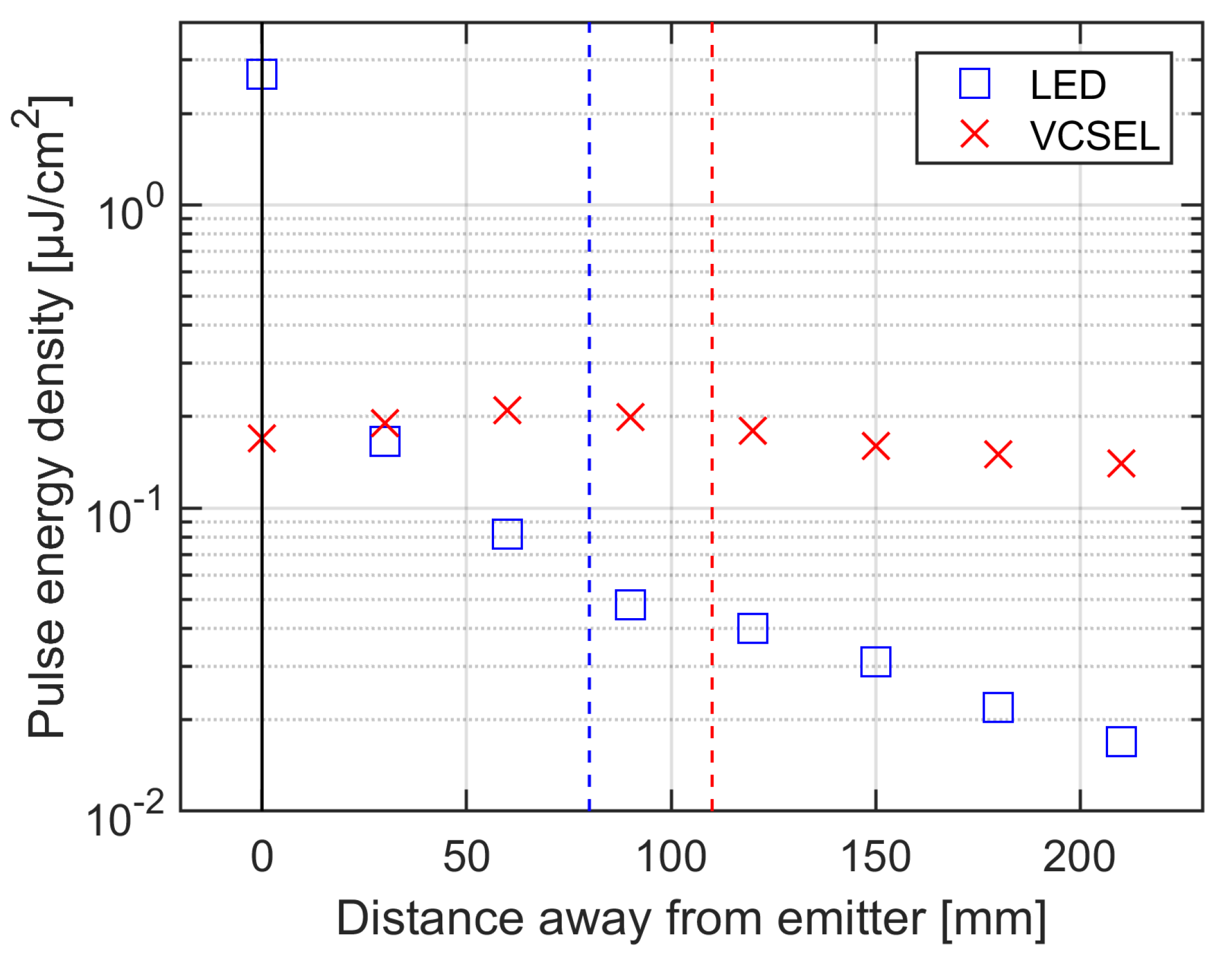
The global quantities reported above do not necessarily correlate with the light intensity at the measurement volume. We therefore measured the energy density at the probe volume for both systems. The energy density integrated over the field of view at 80 mm from the LED window cover is 0.004 / per pulse, under the pulse specifications given above. Inserting the 16 mm focal length aspheric condenser lens improves this figure to 0.058 /. These results confirm both the magnitude of the improvement brought by the aspheric condenser lens, as well as the significant energy loss at the probe volume, over 99%, as predicted by the ray tracing simulations. Despite comparable total pulse energy at the source (0.38 , compared to 0.34 for the LED), the VCSEL-based illumination system delivers 0.18 / per pulse at the probe volume, or more than three times the energy density of the LED system. As anticipated from Figure 3, the low divergence of the laser illumination should result in only minor energy loss over distances relevant to long-distance microscopy. In contrast, the high divergence of the LED illumination system, despite the 16 mm focal length aspheric condenser lens, results in high energy losses at distances away from the emitter. Figure 5 reports the energy density per pulse measured as function of distance for the LED and VCSEL illumination system, according to the configurations given above (see Figure 2 and Figure 3). The respective object planes for both illumination configurations are represented by vertical dash-lines, in blue color for the LED illumination system and red for the VCSEL.
The results of Figure 5 confirm the fairly constant energy density for the VCSEL illumination system, and they highlight the decrease in energy density with distance for the LED system. Interestingly, the energy density as function of distance for the VCSEL illumination is not monotonic, but first increases and then decreases. This trend is the result of the optical arrangement with the plano-concave lens merging the beams from the six laser units, producing an energy density maximum at the converging location, as suggested by the ray tracing simulations. Note that although the VCSEL radiation output could be optimized to maximize energy density at the object plane, the spatial intensity distribution was more uniform when the peak energy density was moved away from the object plane. The logarithmic scale on the energy density axis of Figure 5 shows a linearly decreasing relationship with distance for the LED illumination, for all measurement points except the one taken right at the emitter. The energy density at the emitter is computed as the total radiation energy measured at the LED emitter in relation to the emitter area, i.e., 12.5 . It should be emphasized that the condenser lens is located between the first two measurement points. The monotonic decreasing trend of the LED profile is expected because the energy density is a function of the illuminated area, which grows with distance. The results highlight the high energy losses as a function of distance with LED lighting, with more than a factor two decrease in energy density as distance doubles. More complex optical configurations to optimally collect and transmit the LED light output have shown improvements, but these are more likely to be effective with a particular set0up, rather than a general imaging system configuration like the one presented in this document.
Note that the illumination intensity distributions were fairly smooth across the field of view for both illumination systems, but that LED was clearly superior with respect to uniformity. With a relative dispersion below 8% across the image for the LED illumination, it represents a substantial advantage compared to the near 25-% dispersion measured with the VCSEL illumination. Intensity dispersion, or fall-off in the present case, is detrimental to the system’s dynamic range and signal-to-noise ratio. In this context, it appears that while VCSEL illumination is adapted to small fields of view, it may compromise illumination distribution, and image quality over larger fields.
4. Imaging System Characterization and Performance
This section presents the results of characterization testing to assess and understand the optical capabilities of the imaging system with the equipment described above, with a focus on comparing its performance when LED or laser illumination is employed. In addition, these tests provide specific information to correlate illumination intensity and camera response, to serve as a basis to assess the necessary illumination intensity or pulse energy at the probe volume to optimize the imaging system’s dynamic range and signal-to-noise ratio. We finally present droplet size measurements from a sample spray with the imaging system described in this manuscript.
4.1. Camera Signal-To-Noise Ratio
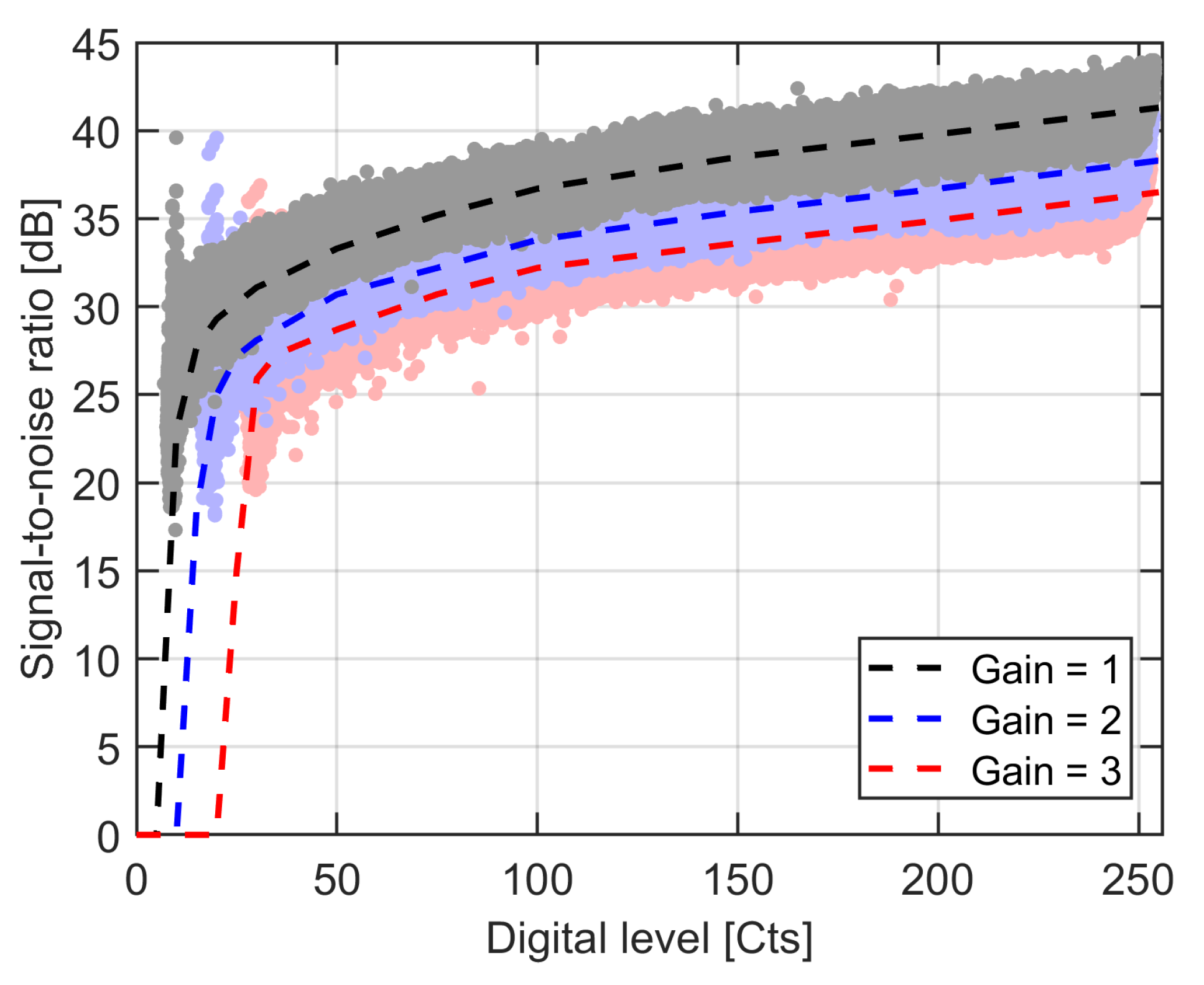
Besides selecting or developing the microscope objective and light source, image quality also relates to the signal-to-noise ratio (SNR) of the imaging device. Under specific conditions, such as the high-speed requirements investigated in this work, the SNR may become critical when gain is applied to the images within the imaging device (in this case at the sensor or camera front-end) to maximize its light sensitivity. Gain generally comes with noise, and too much noise may compromise the image quality, taxing the image processing methods to extract information from the acquired data. We therefore measured the SNR as a function of digital level (8-bit scale) using the following expression,
In Equation (2), and are the mean and standard deviation of the signal S, respectively. To measure the SNR across the dynamic range of the camera, the sensor was illuminated with a diagonal intensity gradient covering the entire dynamic range. The SNR was then computed applying Equation (2) on all pixels of the sensor, except when pixels reached the top-end of the 8-bit digital scale (255 Cts). We repeated the experiments at several gain settings, from a gain level of 1 (or no gain), to a gain level of 3. The results are reported in Figure 6, showing the SNR for all pixels, represented by the dots, as well as the mean profile (dashed-lines) as function of digital intensity.
The results of Figure 6 demonstrate that the camera exhibits excellent SNR, with a mean peak SNR of 41.3 dB with a conversion gain of 1. Current standards for digital camera systems consider 40 dB as excellent SNR, whereas 10 dB would represent an acceptable SNR level. This represents a dynamic range of 120:1, supporting the 8-bit (256 levels) ADC operation as the appropriate digitization mode. At the same time, it would be interesting to evaluate the same camera with the sensor’s ADCs operating at 10- and 12-bit digitization level to conclude whether the increased bit-depth effectively provides usable image information. As expected, SNR drops with higher gain settings, by approximately 3 dB for a gain of 2 and a total of 5 dB from baseline to the SNR measured with a gain of 3; though these still represent good SNR behavior. Looking at the SNR data at the low-end of the graph, we observe that the background level increases with higher gain settings, which is in fact where a large part of the difference in top-end SNR comes from. Despite not being observable on the scatter results of Figure 6, all three gain-specific distributions present similar dispersion, with a marginal increase in standard deviation for the SNR at a gain level of 3.
4.2. Photonic to Digital Relationship
CMOS (or CCD) sensors are based on metal-oxide semiconductor technology, which means that field effect transistors are employed to gate the charge coming from the semiconductor, i.e., the photosensitive area. The photo-site material (semiconductor), used in most modern cameras operating in visible light, is silicon. Silicon is used because its valance to conduction energy gap, or bandgap, of 1.1 eV is near ideal for wavelengths in the visible or near infrared. This means that when a photon of higher energy (above 1.1 eV, or below 1127 nm) hits the surface of the silicon, that photon is absorbed in the silicon and generates a charge. The silicon is doped with different materials with positive and negative charges to create a diode-like structure. The pixel charge is related to the amount of photons hitting the photosensitive area, and being converted by the semiconductor. The conversion efficiency is generally referred to as quantum efficiency (QE). The fill factor is another key information to assess overall photonic conversion efficiency; it represents the fraction of the photosensitive area compared to the effective pixel area. Microlenses are commonly used to collect the light signal and direct it onto the photo-site, effectively improving the fill factor.
CMOS sensors read the charge out under the form of voltage or current directly on the pixel, next to the photo-site. This allows parallel readout, as opposed to the sequential readout used in CCD sensors, a major advantage when it comes to speed. Several transistors are employed to perform the necessary operations to read and move the charges, as well as commonly available features in recent cameras such as gate transfer or global shutter. Global shutter means that all pixels are exposed at the same time, which is important in high-speed applications [16], including the current study. After the charge has been converted to voltage, it is further amplified, and sent to the on-chip analog-to-digital converters (ADC). Each photonic-derived voltage coming from a pixel is converted into digital format based on the level and ADC bit-depth (e.g., 8-bit). Readout rate is in principle related to the number of ADCs, as well as their operating frequency. The camera sensor used in this work features 64 ADCs, all of which can be operated at rates up to 600 MHz, for parallelized and fast conversion. The digital information is then transferred to the computer or directly saved to a high-speed storage system. As commented earlier, the high readout rate of the camera used in this study (18.9 Gbit/s) requires advanced hardware and data handling methods to be sustained.
To relate the photonic energy measured at the probe volume to a digital level, and estimate the light losses through the microscope objective, fundamental characteristics of the sensor are needed. The camera sensor is specified to feature a full well depth (charge) of 13.5 , a sensitivity of 4.64 , and a conversion factor of 0.075 bit/ (for 10-bit digitization). Other parameters such as dark noise, dark current, and fixed pattern noise are insignificant compared to the light-induced charge or the measured digital quantities at the current camera settings. The various noise sources are included as a global noise level under the current camera settings and reported in Figure 6. The absolute (or effective) QE combines the fill factor (including the microlens) and the conversion efficiency of the sensor from photon (light) to charge, i.e., the QE. The absolute QE of the sensor at the LED illumination wavelength (455 nm) is on the order of 43%, whereas the peak QE is near 47%, at 550 nm wavelength. As expected for visible camera sensors, the QE is much lower in the near-infrared wavelength range of the VCSEL, with values on the order of 16% according to the sensor specification document.
Based on the digital resolution of the system, the area of a pixel at the object plane is 6.25 . Considering the measured energy density per pulse at the object plane for the LED illumination system (c.f. Figure 5), the energy going through a virtual pixel at the object plane is slightly more than 3.6 × nJ. On the other hand, the energy going through a virtual pixel at the object plane with the VCSEL illumination system is 1.1 × nJ, a significant gain compared to LED lighting. To understand what these quantities represent in front of the energy necessary to illuminate a pixel at the image plane, the Planck–Einstein relationship can be used as it relates fundamental quantities such as the photon energy E, at a particular wavelength, and is expressed as
where h is the Planck constant, c is the speed of light in vacuum, and is the illumination wavelength. With the illumination wavelength taken as the center wavelength of the LED radiation (455 nm), or at the specified VCSEL radiation wavelength (860 nm), each photon carries an energy on the order of 4.37 × J for LED and 2.31 × J for VCSEL illumination. The respective number of photons going through a virtual pixel at the object plane was on the order of 8200 for the LED illumination, while it was over 48,000 for the VCSEL light source.
Assuming a conversion gain of 1 with the sensor’s ADCs operating under 8-bit mode, the conversion factor is 0.0187 bit/, meaning that each pixel would reach digital saturation (255 Cts) by accumulating a total of nearly 32,000 photons at the LED illumination wavelength, and over 85,000 photons at the VCSEL wavelength. The number of photons necessary to reach full dynamic range of the camera sensor is approximately four times higher than the measured LED light energy at over a virtual pixel at the object plane, and a little under twice the energy delivered by the VCSEL illumination system. These quantities assume that the light between the object and image planes suffer no loss. Comparing these results to the digital level measured by the camera indicates that ~80% of the energy with LED lighting is being lost between the object and image planes. The losses are likely explained by a higher than anticipated dispersion of the diffuse illumination distribution, resulting in lower light energy entering the microscope objective, as well as losses within the microscope objective as a result of the diffuse illumination distribution. Conversely, the VCSEL lighting only appeared to suffer an energy loss below 10% between the object plane and the sensor, demonstrating the efficient energy transmission beyond the probe volume and inside the microscope objective.
In both cases, some amount of gain needs to be applied to the camera sensor to maximize signal-to-noise ratio and effective dynamic range. We applied a gain level of 3 for the LED illumination, and a 40-% gain when using the VCSEL illumination system.
4.3. Optical Resolution and Depth of Field
One of the most important parameters in microscopy is the effective spatial resolution of the system, or how small a feature the device can reliably detect and quantify. Several metrics and methods have been proposed to assess image resolution [18]. The Rayleigh diffraction limit, given earlier in the manuscript (c.f. Section 2), provides theoretical information about the absolute spatial resolution limit of the system. It represents the resolution limit a properly setup imaging system can achieve according to its specifications, namely, the numerical aperture and illumination wavelength [18].
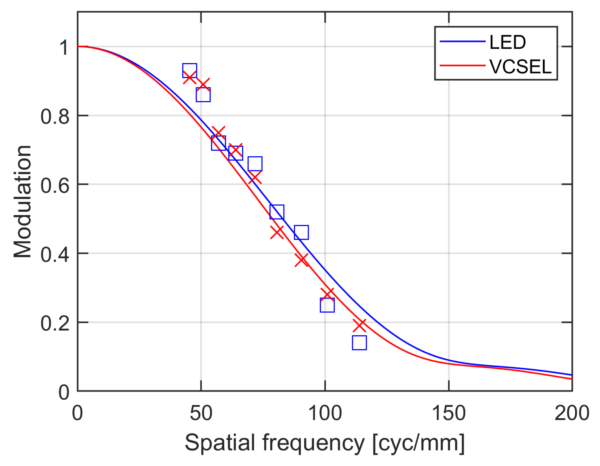
The modulation transfer function (MTF) of a system is metric available to estimate its optical resolution from a practical standpoint. The MTF is a representation of the modulation frequencies that can be resolved by an optical system in the Fourier (frequency) domain. As commented above, the MTF profile of a properly setup microscope system should coincide with the Rayleigh resolution limit approaching zero modulation. We used two methods to evaluate the MTF: The USAF-1951 resolution chart and the knife-edge methods [23]. Both the distribution, in terms of the diffuse angular properties, and the wavelength of the illumination affect optical resolution [22] are two competing parameters when assessing the resolution performance of the LED and VCSEL illumination systems used in this work. The MTF resolution results for both LED and VCSEL illumination are reported in Figure 7.
The modulation transfer function results of Figure 7 show that the intensity contrast decreases as expected from full modulation to below 20% contrast at ~120 cyc/mm. Half modulation is achieved at spatial frequencies near 70 cyc/mm. The results from the knife edge method or the USAF-1951 resolution chart are very similar for both the LED and VCSEL-based illumination systems, meaning that the differences from a practical resolution performance standpoint should be minimal. Considering the differences in wavelength, one would expect higher resolution benefits in favor of the LED illumination configuration. This means that, although the imaging system is indeed diffraction-limited for the VCSEL illumination, the sensor-driven Nyquist frequency limit effectively reduces the resolution performance of the imaging system when LED lighting is employed. Another aspect mentioned above is the impact of diffuse lighting on resolution. Although the diffuse aspect of the illumination distribution, important with the LED system, has been shown to negatively affect resolution, it has not been thoroughly quantified [22]. More work is needed in this area to fully optimize a microscope imaging system when diffuse lighting is used. We remind the reader that diffuse lighting is employed in applications where obscuration or other aspects may compromise image quality at the probe volume, such as dense particle fields, high pressure and temperature environments, or long working distances.
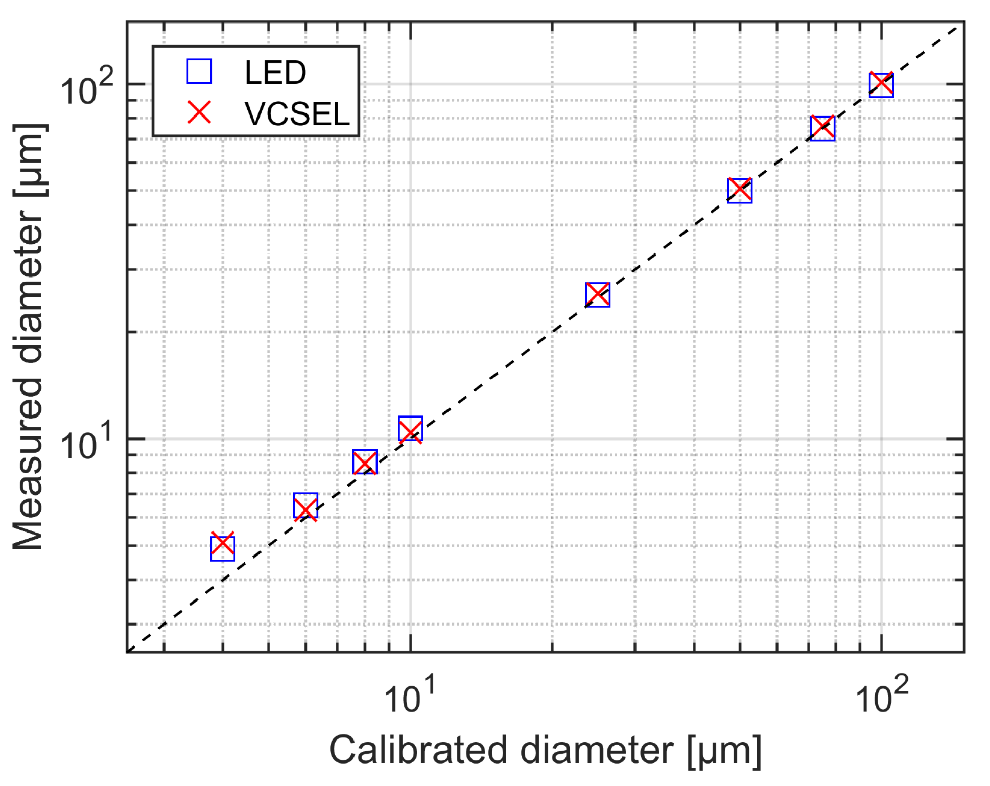
The resolution performance results indicate that the microscope imaging system should be able to resolve features as small as 4 to 5 . To provide more information about the system’s capabilities to detect and quantify small drops or particles, we imaged calibrated opaque disks of various diameters printed on a transparent glass substrate. The printed face of the substrate was located at the object plane and the images with the opaque disks were analyzed to extract equivalent diameter [23]. Figure 8 presents a comparison between measured and calibrated disk diameters when illuminating the scene with both the LED and VCSEL systems.
We imaged disks ranging from 2 to 100 , but disks below 4 were not reliably detected by the system. This is in agreement with the findings of Figure 7. It is important to note that despite being detected and measured, the 4- disk’s measured diameter deviated from the calibrated size by more than 20% (4.9 ). It is unclear if the inaccuracy at such small length scale comes from a fundamental resolution limit of the system, or because of the limited number of pixels to resolve such a small feature (an area equivalent to approximately 2 pixels).
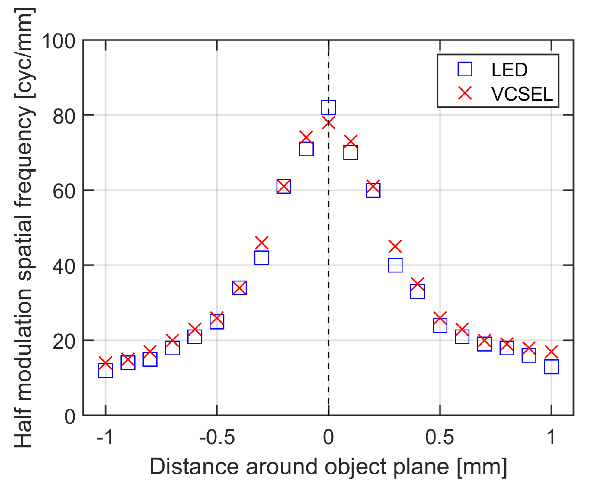
For drop or particle sizing applications, such as the current work, the response of an imaging system with respect to out-of-focus features is yet another important aspect. It is well known that image sharpness, in other terms the effective resolution, degrades when imaging objects away from the object plane. This aspect can be characterized by evaluating the MTF of the system at various depth around the object plane. To synthesize the information, Figure 9 plots the spatial frequency the system can resolve with a half intensity difference, or the spatial frequency at half modulation, as function of the distance on both sides of the object plane.
Figure 9 confirms the marginal differences between LED and VCSEL-based illumination when it comes to resolution and depth of field. The subtle difference in peak spatial frequency at 50% modulation was already appreciated in Figure 7, whereas the slightly wider distribution of the VCSEL in Figure 9 can be explained by the increased distance to the microscope objective (due to chromatic focus shift). The results of Figure 9 show how quickly spatial resolution deteriorates as an imaged object is moved away from the plane of optimal focus. The spatial frequency at 50% modulation approaches half its peak value only about 0.3 mm away from the object plane. Even with such degradation in spatial resolution, the test results still indicate that the system should be able to resolve features on the order of 10 over half a millimeter around the object plane.
4.4. Sample Spray Experiments
To demonstrate the capabilities and performance of the imaging system, we performed droplet size measurements. The droplet field was generated by an air-operated spray system (airbrush). An airbrush operates with a flow of compressed air passing through a venturi, which creates a low-pressure region, pulling liquid, in this case water, from a directly-connected reservoir. The high-velocity air flow contributes to the fine breakup of the liquid stream into small droplets, appropriate for the size range of the imaging system presented herein. The airbrush was operated with an air pressure of 1.70 atm and an air flow of 10 L/min. The measurements were performed on axis with the droplet stream coming out of the airbrush nozzle, at a distance of approximately 50 mm. Both illumination systems (LED and VCSEL) were used to compare their performance in practical conditions.
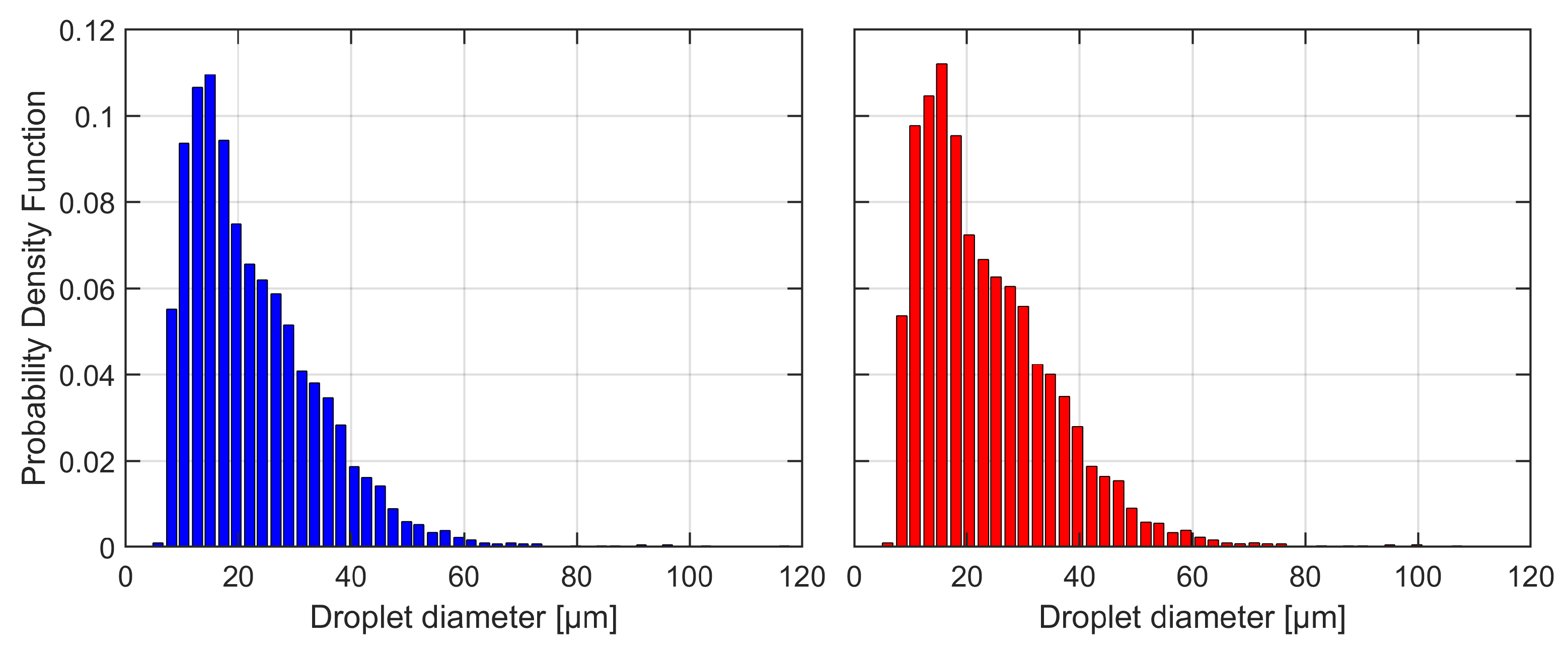
The images were processed according to the image processing methods developed by the authors and described in detail in [23], and summarized in the following lines. A dynamic background correction based on a three-level temporal derivative scheme is applied first to compensate dynamic changes in intensity distribution, acting as a normalization scheme. The droplet detection method is based on a modified Moore Neighborhood algorithm with optimized stopping criteria for boundary tracing [24]. Detected droplets are kept with their surrounding area, and the local two-dimensional attenuation distribution is computed for each droplet. The attenuation distributions are analyzed to extract peak attenuation and edge gradient criteria. These two parameters are used simultaneously to limit the depth of field and associated out-of-focus sizing uncertainty to below 5% over the imaging system’s size range. The results of the tests performed with the airbrush are shown in Figure 10. The left size histogram reported the droplet size distribution measured when LED illumination was employed, whereas the right plot shows the results with the VCSEL illumination system. The results are presented as probability density function, as opposed to droplet counts, to assist with the comparison. A single, 5-s long acquisition (~500 frames) was recorded in both experimental configurations, resulting in detecting and measuring approximately the same number of drops with both illumination systems: 4225 droplets for LED and 4177 for VCSEL.
The two droplet size distributions reported in Figure 10 are visually very similar. They both present the typical log-normal distribution profile expected in flow-driven liquid breakup conditions. The smallest droplet measured by the imaging system with LED illumination was 5.6 , whereas it was 6.0 with VCSEL illumination. The largest was 114 and 117 for LED and VCSEL illumination, respectively. These droplet diameter differences are more likely related to a particular event difference than actual differences in instrumentation performance using one illumination system or another. Similarly, the arithmetic mean diameter was 21.1 when using LED illumination, and 21.9 when the VCSEL illumination system was employed. Under the present imaging system set-up and experimental configuration, both illumination systems performed similarly, and the results appear not to be compromised by the shortcomings of one illumination solution compared to the other.
5. Conclusions
This work investigated the characteristics and performance of a long-distance microscope imaging system optimized for quantification of droplets and particle fields in high-speed flows. We developed and thoroughly characterized two ultrafast illumination systems based on light-emitting diode (LED) and vertical-cavity surface-emitting lasers (VCSEL). The illumination systems were designed to generate short light pulses with energetic and spatial distribution properties optimized for line-of-sight, long-distance microscope imaging. We selected a state-of-the-art long-distance microscope lens to be mounted onto a high-resolution (12 Mpix), high-throughput (2.37 Gpix/s) machine-vision camera, for a final digital resolution of 2.5 /pix. The relatively simple optical setup on the illumination side was aided by ray tracing simulations, enabling object plane energy densities sufficient to use short (50 ns) light pulses to illuminated the scene. Energy transmission measurements demonstrated the high energy losses with the LED system, whereas the laser-based illumination maintained fairly constant energy density as function of distance. We provided estimates regarding the energy delivered by the illumination systems to the object and image planes, and correlations between illumination intensities and recorded digital levels, as measured by the camera system. The laboratory experiments to characterize the imaging system with both illuminations devices showed that the system was near diffraction-limited when VCSEL illumination was used, although it was likely limited by digital resolution, and possibly the diffuse aspect of the illumination when using LED lighting. Both illumination solutions provided comparable performance with respect to resolution, detectability, and sizing accuracy, as well as depth-of-field. Droplet sizing measurements performed on a sample droplet field generated by an airbrush confirmed these findings, with very similar droplet size distributions measured when the droplet field was illuminated with the LED or VCSEL illumination systems.
Author Contributions
Conceptualization; methodology; validation; formal analysis; investigation; data curation; writing—original draft preparation; visualization; supervision; project administration; funding acquisition by J.M. Writing—review and editing; supervision; project administration; funding acquisition by W.D.B. All authors have read and agree to the published version of the manuscript.
Funding
This research was funded by NASA Shared Services Center (NSSC) contract numbers 80NSSC19C0019 and 80NSSC19C0032.
Acknowledgments
The authors are grateful for the financial support by NASA Glenn Research Center through several research projects and contracts, including NASA Shared Services Center (NSSC) SBIR Phase III contracts.
Conflicts of Interest
The authors declare no conflict of interest.
References
- Ashgriz, N. Handbook of Atomization and Sprays: Theory and Applications; Springer Science & Business Media: Berlin, Germany, 2011. [Google Scholar]
- Lefebvre, A.H. Atomization and Sprays; CRC Press: New York, NY, USA, 1989. [Google Scholar]
- Pawlowski, L. The Science and Engineering of Thermal Spray Coatings; John Wiley & Sons: Hoboken, NJ, USA, 2008. [Google Scholar]
- Li, Q.; Yuan, C.; Tao, Q.; Zheng, Y.; Zhao, Y. Experimental analysis on post-explosion residues for evaluating coal dust explosion severity and flame propagation behaviors. Fuel 2018, 215, 417–428. [Google Scholar] [CrossRef]
- Cziczo, D.J.; Ladino, L.; Boose, Y.; Kanji, Z.A.; Kupiszewski, P.; Lance, S.; Mertes, S.; Wex, H. Measurements of ice nucleating particles and ice residuals. Meteor. Mon. 2017, 58, 8.1–8.13. [Google Scholar] [CrossRef] [Green Version]
- Chen, G.; Mazumder, M.; Chang, R.K.; Swindal, J.C.; Acker, W.P. Laser diagnostics for droplet characterization: Application of morphology dependent resonances. Prog. Energ. Combust. 1996, 22, 163–188. [Google Scholar] [CrossRef]
- Linne, M. Imaging in the optically dense regions of a spray: A review of developing techniques. Prog. Energ. Combust. 2013, 39, 403–440. [Google Scholar] [CrossRef]
- Durst, F.; Zare, M. Laser Doppler measurements in two-phase flows. In Proceedings of the LDA-Symposium, Copenhagen, Grenoble, France, 30 March–2 April 1976; pp. 403–429. [Google Scholar]
- Bachalo, W.D.; Houser, M.J. Development of the phase/Doppler spray analyzer for liquid drop size and velocity characterizations. In Proceedings of the AIAA, SAE, and ASME, Joint Propulsion Conference, Cincinnati, OH, USA, 11–13 June 1984. [Google Scholar]
- Cruyningen, I.; Lozano, A.; Hanson, R.K. Quantitative imaging of concentration by planar laser-induced fluorescence. Exp. Fluids 1990, 10, 41–49. [Google Scholar] [CrossRef]
- Greenhalgh, D. Planar measurements of fuel vapour, liquid fuel, liquid droplet size and soot. In Proceedings of the Planar Optical Measurement Methods for Gas Turbine Components, Cranfield, UK, 16–17 September 1999; pp. 1–7. [Google Scholar]
- Kim, H.; Westerweel, J.; Elsinga, G.E. Comparison of Tomo-PIV and 3D-PTV for microfluidic flows. Meas. Sci. Technol. 2012, 24, 024007. [Google Scholar] [CrossRef]
- Seifi, M.; Fournier, C.; Grosjean, N.; Mees, L.; Marie, J.L.; Denis, L. Accurate 3D tracking and size measurement of evaporating droplets using in-line digital holography and “inverse problems” reconstruction approach. Opt. Express 2013, 21, 27964–27980. [Google Scholar] [CrossRef] [PubMed]
- Van De Hulst, H.C. Light Scattering by Small Particles; Dover Publications, Inc.: New York, NY, USA, 1981. [Google Scholar]
- Wriedt, T. A review of elastic light scattering theories. Part. Part. Syst. Charact. Meas. Descr. Part. Prop. Behav. Powders Other Disperse Syst. 1998, 15, 67–74. [Google Scholar] [CrossRef]
- Manin, J.; Skeen, S.A.; Pickett, L.M. Performance comparison of state-of-the-art high-speed video cameras for scientific applications. Opt. Eng. 2018, 57, 124105. [Google Scholar] [CrossRef]
- Carlen, C.R. High-Speed, High-Current Pulsed Driver Circuit. US Patent 9,603,210, 21 March 2017. [Google Scholar]
- Murphy, D.B. Fundamentals of Light Microscopy and Electronic Imaging; John Wiley & Sons: Hoboken, NJ, USA, 2002. [Google Scholar]
- Nayar, S.K.; Ben-Ezra, M. Motion-based motion deblurring. IEEE Trans. Pattern Anal. Mach. Intell. 2004, 26, 689–698. [Google Scholar] [CrossRef] [PubMed]
- Wong, W.P.; Halvorsen, K. The effect of integration time on fluctuation measurements: Calibrating an optical trap in the presence of motion blur. Opt. Express 2006, 14, 12517–12531. [Google Scholar] [CrossRef] [PubMed] [Green Version]
- Bachalo, W.D.; Payne, G.A.; Ibrahim, K.; Fidrich, M.J.; Manin, J. Particle Field Imaging and Characterization Using Vcsel Lasers for Convergent Multi-Beam Illumination. US Patent App. 15/959,717, 24 October 2019. [Google Scholar]
- Westlye, F.R.; Penney, K.; Ivarsson, A.; Pickett, L.M.; Manin, J.; Skeen, S.A. Diffuse back-illumination setup for high temporally resolved extinction imaging. Appl. Optics 2017, 56, 5028–5038. [Google Scholar] [CrossRef] [PubMed] [Green Version]
- Manin, J.; Bachalo, W.D. Advances in imaging diagnostics for icing research in aircraft engines. In Proceedings of the ILASS-Americas 2019, Tempe, AZ, USA, 12–15 May 2019. [Google Scholar]
- Reddy, P.R.; Amarnadh, V.; Bhaskar, M. Evaluation of stopping criterion in contour tracing algorithms. Int. J. Comput. Sci. Inf. Technol. 2012, 3, 3888–3894. [Google Scholar]
Figure 1.
Relationship between travel time and object velocity for a range of linear displacements (see legend) relevant to microscopy in high-speed flows. This graph provides guidance to limit motion blurring to image moving objects at different spatial resolutions.
Figure 1.
Relationship between travel time and object velocity for a range of linear displacements (see legend) relevant to microscopy in high-speed flows. This graph provides guidance to limit motion blurring to image moving objects at different spatial resolutions.

Figure 2.
Ray tracing simulation showing the output radiation of the light-emitting diode (LED) emitter on the left. The LED output is collected and transmitted by a 16 mm focal length condenser lens. The probe volume is shown in red and the microscope objective’s effective collection is represented by a dark gray rectangle.

Figure 3.
Ray tracing simulation showing the output radiation of the multi-beam laser illumination system. The collimated and oriented laser beams enter from the left and are merged together by a −200 mm plano-concave lens. The probe volume is shown in red and the microscope objective’s effective optical collection is represented by a dark gray rectangle.

Figure 4.
Measured pulse profiles for a 50 ns pulse duration with both LED and vertical-cavity surface-emitting laser (VCSEL) illumination systems developed in our laboratories.
Figure 4.
Measured pulse profiles for a 50 ns pulse duration with both LED and vertical-cavity surface-emitting laser (VCSEL) illumination systems developed in our laboratories.

Figure 5.
Energy density measurements as function of distance away from the emitter for the LED (c.f. Figure 2), and away from the plano-concave lens for the VCSEL illumination system (c.f. Figure 3). The object planes for both illumination systems are indicated as dashed-lines, blue for LED and red for the VCSEL configuration.

Figure 6.
Signal-to-noise ratio as a function of digital intensity for the camera at various gain settings. The data points have been calculated from Equation (2), and the dashed-line profiles represent the mean of the scatter distributions.
Figure 6.
Signal-to-noise ratio as a function of digital intensity for the camera at various gain settings. The data points have been calculated from Equation (2), and the dashed-line profiles represent the mean of the scatter distributions.

Figure 7.
Modulation transfer function of the imaging system at the object plane with both the LED and VCSEL illumination systems. The results report the modulation transfer function (MTF) evaluated with both the knife-edge method and the USAF-1951 resolution chart.
Figure 7.
Modulation transfer function of the imaging system at the object plane with both the LED and VCSEL illumination systems. The results report the modulation transfer function (MTF) evaluated with both the knife-edge method and the USAF-1951 resolution chart.

Figure 8.
Measured diameter comparisons with calibrated diameter for metal-printed opaque disks of various diameters ranging from 4 to 100 . These measurements were performed with the scene illuminated by the LED and VCSEL light sources.
Figure 8.
Measured diameter comparisons with calibrated diameter for metal-printed opaque disks of various diameters ranging from 4 to 100 . These measurements were performed with the scene illuminated by the LED and VCSEL light sources.

Figure 9.
Depth of field measurements evaluated as the spatial frequency at half modulation as function of distance around the object plane. The modulation transfer function was measured via the knife edge method with both the LED and VCSEL light sources.
Figure 9.
Depth of field measurements evaluated as the spatial frequency at half modulation as function of distance around the object plane. The modulation transfer function was measured via the knife edge method with both the LED and VCSEL light sources.

Figure 10.
Histograms of droplet size distributions measured by the imaging system for an example droplet field generated by an air-operated nozzle. The left histogram was acquired with the droplet field illuminated by the LED light source, whereas the VCSEL system was used to generate the right histogram.

© 2020 by the authors. Licensee MDPI, Basel, Switzerland. This article is an open access article distributed under the terms and conditions of the Creative Commons Attribution (CC BY) license (http://creativecommons.org/licenses/by/4.0/).
Share and Cite
MDPI and ACS Style
Manin, J.; Bachalo, W.D. Advances in Imaging Diagnostics for Spray and Particle Research in High-Speed Flows. Appl. Sci. 2020, 10, 1450. https://0-doi-org.brum.beds.ac.uk/10.3390/app10041450
AMA Style
Manin J, Bachalo WD. Advances in Imaging Diagnostics for Spray and Particle Research in High-Speed Flows. Applied Sciences. 2020; 10(4):1450. https://0-doi-org.brum.beds.ac.uk/10.3390/app10041450
Chicago/Turabian StyleManin, Julien, and William D. Bachalo. 2020. "Advances in Imaging Diagnostics for Spray and Particle Research in High-Speed Flows" Applied Sciences 10, no. 4: 1450. https://0-doi-org.brum.beds.ac.uk/10.3390/app10041450
Note that from the first issue of 2016, this journal uses article numbers instead of page numbers. See further details here.