
Roadmapping of Nanoelectronics for the New Electronics Industry

1
IEEE IRDS, IEEE 445 Hoes Lane, Piscataway, NJ 08855, USA
2
CNRS, Grenoble INP, University Grenoble Alpes, European Sinano Institute, 3 Parvis Louis Neel, 38016 Grenoble, France
3
Faculty of Science and Technology, Keio University, 2-15-45 Mita, Minato-ku, Tokyo 108-8345, Japan
*
Author to whom correspondence should be addressed.
Appl. Sci. 2022, 12(1), 308; https://0-doi-org.brum.beds.ac.uk/10.3390/app12010308
Submission received: 4 November 2021
/
Revised: 17 December 2021
/
Accepted: 20 December 2021
/
Published: 29 December 2021
(This article belongs to the Special Issue Advances in Microelectronic Materials, Processes and Devices)
Abstract
:This paper is dedicated to a review of the international effort to map the future of nanoelectronics from materials to systems for the new electronics industry. The following sections are highlighted: the Roadmap structure with the international teams, the methodology and historical evolution, the various eras of scaling, the new ecosystems and computer industry, the evolving supply chain, the development of SoC and SiP, the advent of the Internet of Everything and the 5G communications, the dramatic increase of data centers, the power challenge, the technology fusion, heterogeneous and system integration, the emerging technologies, devices and computing architectures, and the main challenges for future applications.
1. Introduction
Roadmaps are absolutely necessary for all high-tech sectors, such as nanoelectronics, in order to improve the links between academia and industry, to stimulate investments, to provide elements for future research programs and activities, and to coordinate efforts to propose the most promising solutions.
Two different strategies can be used for the roadmapping process: starting from the requests of application experts to address various societal challenges and find the technologies that can satisfy the required function performance for each application, or starting from the planned technological evolution to propose disruptive applications.
The combination of a top-down, application-oriented approach and a bottom-up approach, based on planned technological change to spark new ideas for disruptive products and applications, can be a good solution.
Various roadmapping activities have been performed these last years in different regions, for example in Japan with SRDJ (System and Device Roadmap of Japan) [1], in Europe with NEREID [2], for the long term Nanoelectronics Roadmap funded by the European Commission and driven by the Sinano Institute, and at international level with the ITRS and IRDS (International Roadmap for Devices and Systems).
The main aim of the ITRS, which ended in 2015, has been to provide guidance to the many players in the semiconductor field, to synchronize technological development and the availability of equipment, as well as to focus on critical challenges.
However, the “technological push” that has been the basis of the ITRS has shown its limits in recent years, and systems-oriented technologies have been taken into account by the new IRDS roadmap (International Roadmap for Devices and Systems), launched in 2016 [3]. On the other hand, the development of novel functionalities for new applications, requires the use of special figure of merits for technologies that do not follow “Moore’s law”, expanding the focus of chips to different types of systems. This novel field has recently been integrated in the IRDS Roadmap.
This article will be devoted to IRDS, which focuses on producing a roadmap of the main building blocks of the electronics industry ranging from devices to systems. The IRDS offers a 15-year perspective that leaves enough time for researchers to find solutions for challenges that lie ahead 10 years in advance and beyond, while providing a range of technology and system alternatives in the short and medium terms. Finally, the IRDS is closely monitoring the progress of the industry over the next 5 years to verify that planned projections were in line with actual implementations adopted in manufacturing by the industry.
2. IRDS Structure
The International Roadmap for Devices and Systems, supported by the IEEE, includes the work of 13 IFTs (International Focus Teams) experts in materials, devices and systems. Led by the IRC (International Roadmap Committee), the IFTs developed the IRDS 2021 roadmap and engaged with other IEEE societies: Rebooting Computing Initiative, Electron Devices Society, Computer Society, Communication Society, as well as with related expert communities such as System and Device Roadmap of Japan (SDRJ) and the European Academic and Scientific Association for NanoElectronics (SINANO Institute) [4] in complementary activities to help ensure alignment and consensus among universities, industry, national laboratories and consortia.
The IRC is made up of representatives from SINANO, SDRJ and IEEE EDS and IEEE CS. The IFTs cover the following areas: AB: Applications Benchmarking, SA: Systems and Architecture, OSC: Outside system Connectivity, MM: More Moore, BC: Beyond CMOS, CEQIP: Cryogenics Electronics and Quantum Information Processing, PI: Packaging Integration, FI: Factory integration, L: Lithography, YE: Improved yield, M: Metrology, ESH/S: Environment, safety, health and sustainability, MtM: More than Moore. Each of the IFTs focuses on technological roadmaps in their specific fields and on cross-border domains. The major revision of the IRDS™ roadmaps is carried out every two years, and minor revisions are performed annually.
3. Roadmap Methodology Background and Historical Evolution
The IRDS is the third generation of the Roadmap, initially described empirically by Gordon Moore in 1965 [5]. His prediction mentioned that the number of transistors that could be integrated into a single chip would double each year for the next ten years. This was found to be true and in 1975 he revised his prediction by doubling the number of transistors every 2 years [6]. He also identified three main contributors to these results: the architecture of integrated circuits, the scaling down of devices, and the ability to produce cost effectively larger dice thanks to high manufacturing efficiencies. Robert Dennard published also some rules for predicting the performance of miniaturized transistors [7]. The semiconductor industry scrupulously followed these rules for the next fifteen years. Dennard’s methodology was correct till about 2005. Inversely, Moore’s Law is still valid today and is predicted to continue to hold for at least the next ten years.
In 1991, it was proposed by the universities, industry and government organizations in the US to write a document with the future evolution governing the next steps of the semiconductor and electronics industries for the next 15 years. Eleven Technology Working Groups (TWGs) were indeed formed for this purpose. In 1992, the National Technology Roadmap for Semiconductors (NTRS) was published, followed by publications in 1994 and 1997.
In 1996 it was clear that major obstacles will be encountered in the next years; for example, the gate dielectric becoming too thin by 2005 at the latest. A full re-engineering of the transistor was necessary to overcome these limits. This was a worldwide problem affecting the entire semiconductor and electronics industries.
The International Technology Roadmap for Semiconductors (ITRS) was formed in 1998 to overcome these roadblocks with the involvement of partners from Europe, Japan, Korea, Taiwan and US. A revolutionary strategy to completely change how transistors are structured and manufactured was proposed. The worldwide collaboration between universities, suppliers, national programs and consortia around allowed the development of strained silicon, high-k/metal-gate, novel device architecture such as FinFET, in manufacturing. In 2011 this effort was finalized and allowed to save the semiconductor and the electronics industry.
Historically, the semiconductor industry provided the needed blocks to system integrators. New products with enhanced performance than the previous ones were enabled by an improved technology. The pace at which the whole electronics industry ecosystem was moving forward was guided by the Integrated device manufacturers (IDM) together with software companies for operating systems and applications. The transistor scaling, the challenges to be overcome, the performance of integrated circuits were forecasted by the NTRS and IRDS Roadmaps.
In the last 15 years, system integrators have regained full control of the business model due to the development of design houses and foundries that have revolutionized the semiconductor industry. System requirements are driving any new product design cycle and related needs are transmitted through the manufacturing production chain to the semiconductor manufacturers. The design of a new PC is presently not triggered by a faster processor, and on the contrary new ICs and other functionalities are required by the design of a new smart phone. On the other hand, limits of traditional 2D integration lead to a substantial challenge for semiconductor industry to continue scaling at historical rates. In 2016, the introduction of new very innovative 3D transistors, memory cells and other 3D IC structures has launched another revolution in the way ICs will be designed and produced in the next decade.
4. The New Computer Industry
Bipolar devices, proposed at the end of the 1940s, were the first transistors fabricated at the beginning of the electronics era. However, the Si CMOS technology, proposed in 1960, were developed in the following decades and became the main one for both logic and memory devices. Nevertheless, in the middle of the first decade of the new century we faced again power limitations inducing performance saturation. The solution to this challenge, which became the standard, was the use of multiple cores processing in parallel, which saved computational performance while retaining reliable power control.
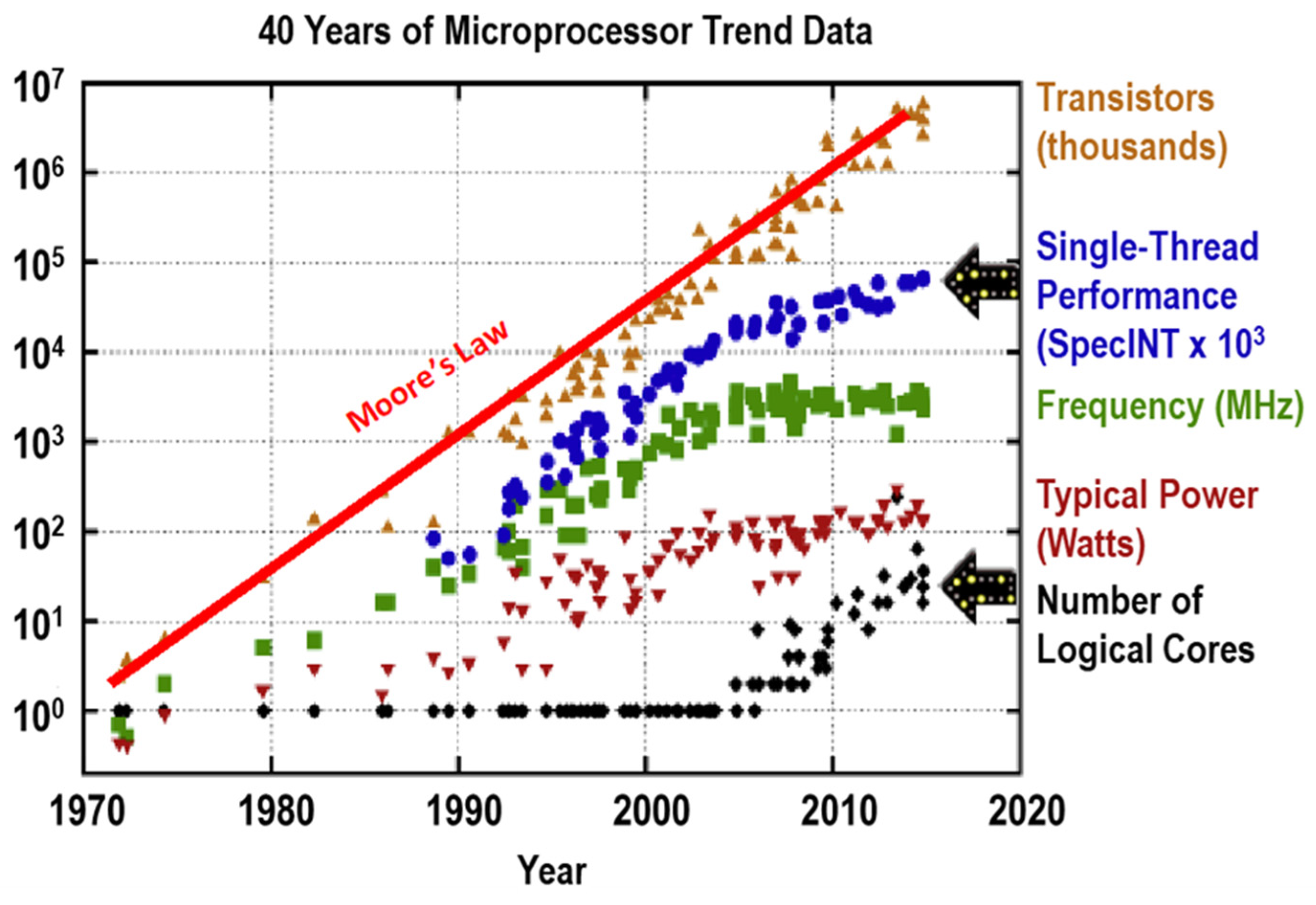
However, the resulting rate of improvement was not as good as the previous ones (Figure 1).
It became clear to system designers that in order to improve performance it was no longer possible to seek for a common solution for many applications, but it was needed to develop alternative architectures, which was not based on the Von Neumann approach proposed in 1945 for solving specific problems. These solutions include neuromorphic computing, approximate computing, reversible computing, in-memory computing, and quantum computing for some special applications.
5. SoC and SiP
In the past 15 years, the electronics industry has substantially changed due to the pervasive deployment of mobile phones, Wi-Fi stations, together with the success of joint work between foundries and fabless companies. Today, the conception, design, and realization of any ICs by system integrators do not need integrated device manufacturers, including the integration of multiple functionalities in a single chip (System on Chip/SoC) or multiple dice in a single package (System in Package/SiP). These strategies of integration allow to reduce the cost and increase the efficiency compared with the assembly of many components on a board (PCB). They also allow to reduce the size of the functionalities for mobile products with confined environments. The development of heterogeneous monolithic integration is more complex than the SiP one and requires one or two more technology generations to be launched. In order to increase system performance, the combination of SoC and SiP could become a cost-effective solution.
System integrators are generally setting the pace for innovation for the electronics industry. The integrated circuit industry has also helped provide innovative technological building blocks to other industries that did not exist or were in their infancy before. Additional functionalities, such as MEMS, flat panel displays, sensors have been provided by the IC industry to other ones, which allowed for the development of the More than Moore (MtM) field, which began to be discussed in 2006 by the ITRS.
6. Power Challenge
In the beginning of the first decade of this century thermal limits have been reached by advanced integrated circuits. It was not possible to simultaneously increase the frequency of operation together with the number of transistors. It was decided to continue to increase the number of devices and to limit the frequency in the range of a few GHz. In the past 5–10 years, novel materials and device architectures have been proposed to alleviate this challenge. Complex software algorithms were also developed to increase performance, changing at the same time the processor architecture from single to multi-core. The combination of the output of the multiple cores, each core operating at a lower frequency, allow to recover the performance for a given application. However, some problems can only use a serial operation, and therefore this strategy does not represent a universal solution.
Nevertheless, communication with mobile devices using Wi-Fi access have been up to now not impacted by these frequency and power limitations, due to their moderate frequency and power operations. However, the development of 5G will significantly change these considerations and these limits will have to be reconsidered.
7. Internet of Things, Internet of Everything (IoT, IoE)
These last 25 years, the Internet has had a revolutionary impact on many domains, including the rise of electronic mail, instant messaging, voice over Internet Protocol (VoIP) telephone calls, and the World Wide Web. The internet has dramatically increased the worldwide connectivity with many new applications in the past 25 years, with data transmissions beyond 40-Gbit/s. A total of 1% of the telecommunicated information was transmitted by internet in 1993 and up to 97% in 2007!
The Internet of Things and of Everything are now leading to ubiquitous communications with the help of innovative functionalities at affordable costs driven by the progress of semiconductor industry. In the future, innovative materials, devices, circuit design, functionalities including autonomous ubiquitous nanosystems, 3D integration, system architectures will lead to a new revolution for the computers and electronic products (see for instance NEREID and Rebooting Computing websites for more details).
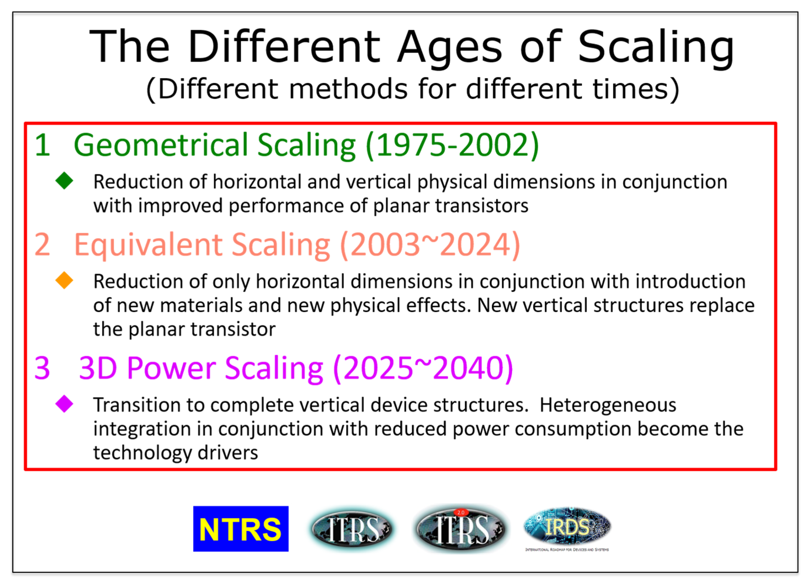
8. The 3 Eras of Scaling
The self-aligned silicon MOSFET planar process was invented in the late 1960s. Geometrical scaling was dominant till the 1990s, with a bottom-up approach for new systems based on continuous increase of the performance of transistors leading to better microprocessors and memory products. However, the MOS transistor was completely restructured in 1998 to overcome identified major bottlenecks.
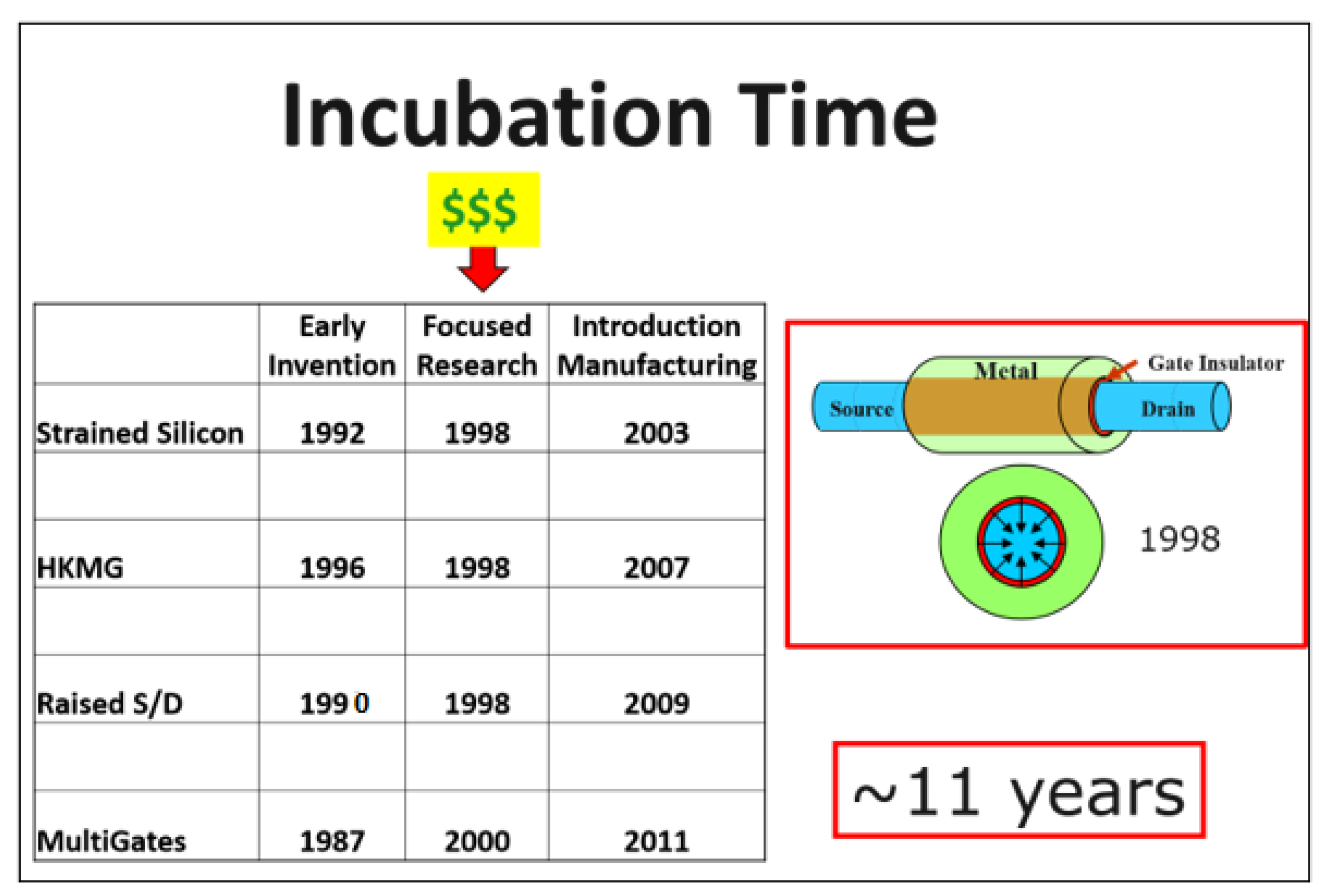
Therefore, a new era, the “equivalent scaling”, based on strained silicon [8,9], high-κ/metal gate [10], raised Source/Drain [11], multigate [12] specially FinFET [13] or Gate-All-Around (GAA) [14], was launched at the end of the 1990s. This novel strategy allows to reduce the historical time of ~25 years for the development of major transistor innovations to less than half in and to save the semiconductor industry, which introduces these innovations by 2011 into high volume manufacturing (Figure 2 and Figure 3).
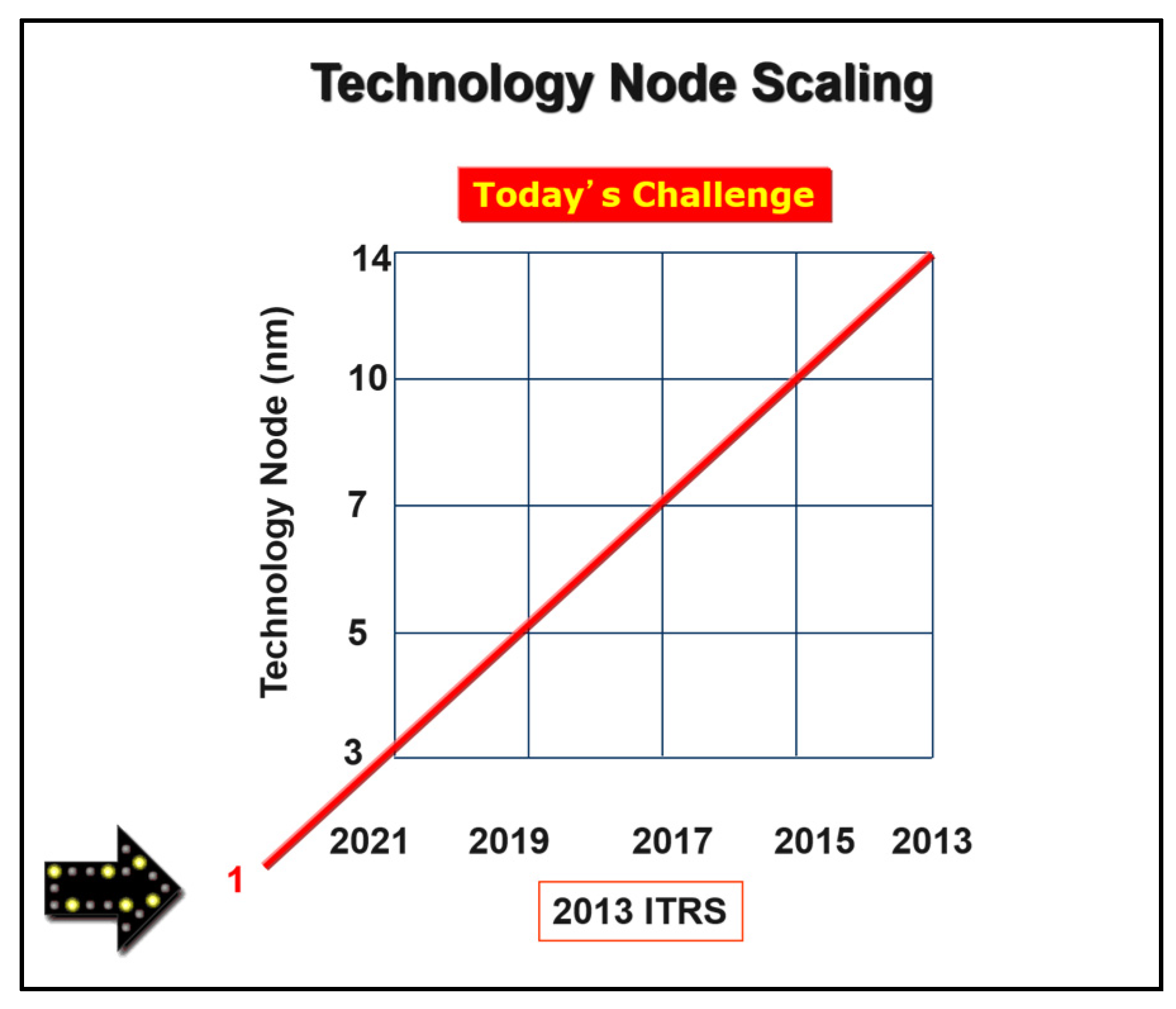
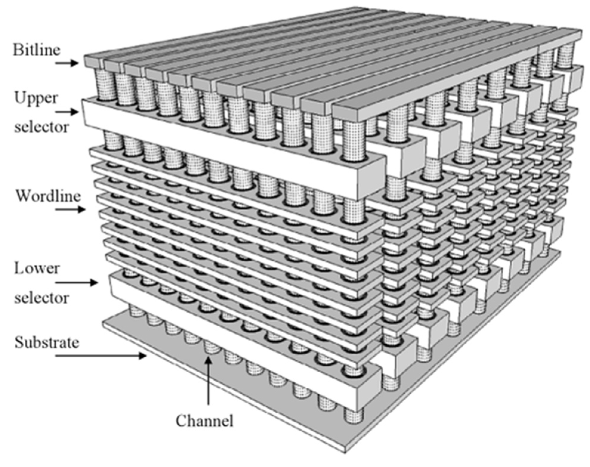
In 2013 ITRS the limits of 2D integration were forecasted with dimension of a few nm planed for the 2020s (Figure 4). Flash memories were the first product facing this problem, and in 2014 announcements were made by several companies that they planned to use the third dimension, launching the third generation of transistor scaling (Figure 5).
The name “3D Power Scaling” was proposed by the IRDS highlighting the future challenges of the semiconductor and electronics industries in the next decades.
Figure 6 shows the three eras of transistor scaling discussed previously.
9. The Continuously Evolving Supply Chain
The semiconductor industry was revolutionized by the development of the PC (personal computer) adopted by consumers having continually different needs for novel products. This was an unprecedented situation for this industry, which was able to respond to these requirements with the combination of Intel as IDM and Microsoft as the software provider. The supply chain model was completely changed by the advent of the iPhone and iPad in 2007 and 2010, respectively, showing that system integrators were able to design their products and chips, followed by a successful foundry manufacturing. Since that time, this new model controls the electronics industry growth.
Cell phones and Wi-Fi notebooks were adopted by the business community and also by consumers. In a single device it is now possible to integrate all the functionalities of the PCs and other equipment, including, pictures, books, songs, etc. Recently, in 2020 due to the pandemic the market of PCs and notebooks has regained a significant growth.
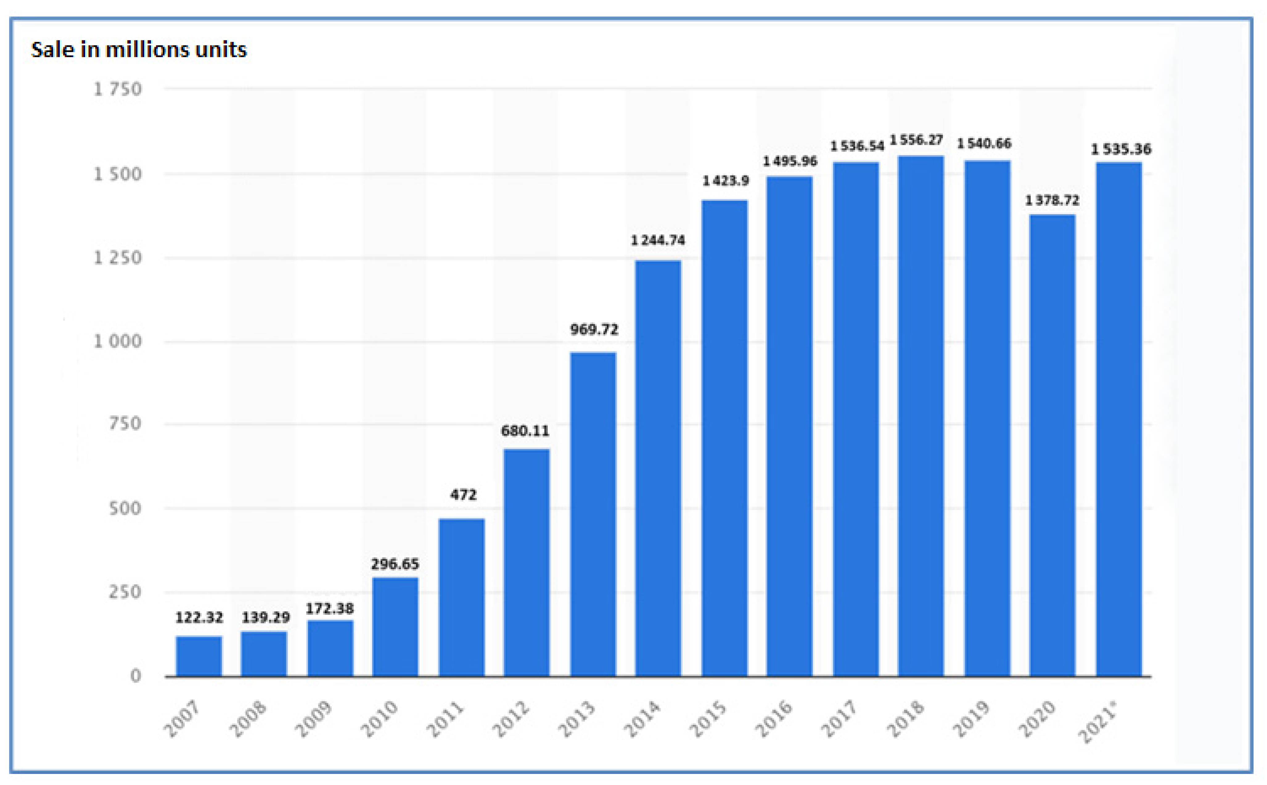
On the other hand, a huge growth was observed from 122 million in 2007 to 1.5 billion smartphones in 2017, with some saturation and a decline for the first time in 2020 (Figure 7).
In recent decades, Moore’s Law has been driven by the downscaling of dimension, innovative circuit architecture, larger die and improvement of the yield. Lithography tools have substantially progressed every 2 years till the advent of EUV (extreme UV) using 13.5 nm illumination, which took a long time to be optimized due to the weakness of power sources to expose wafers fast enough needed for economic purposes, in order to avoid multiple exposures. Flash memory producers used these last years a workaround by stacking more than 100 memory cells on top of each other in order to obtain a high density without the use of the most advanced lithography tools; this solution is not adopted yet by logic manufacturers. The EUV equipment was launched in 2018 in pilot lines, using a power source of more than 100 watts. Several tens of tools were recently delivered in high volume manufacturing lines, able to resolve lines and space with a single exposure with a 36 nm pitch, corresponding to the 18 nm node using the right definition. However, the industry misnamed this technology generation using the 5 nm label.
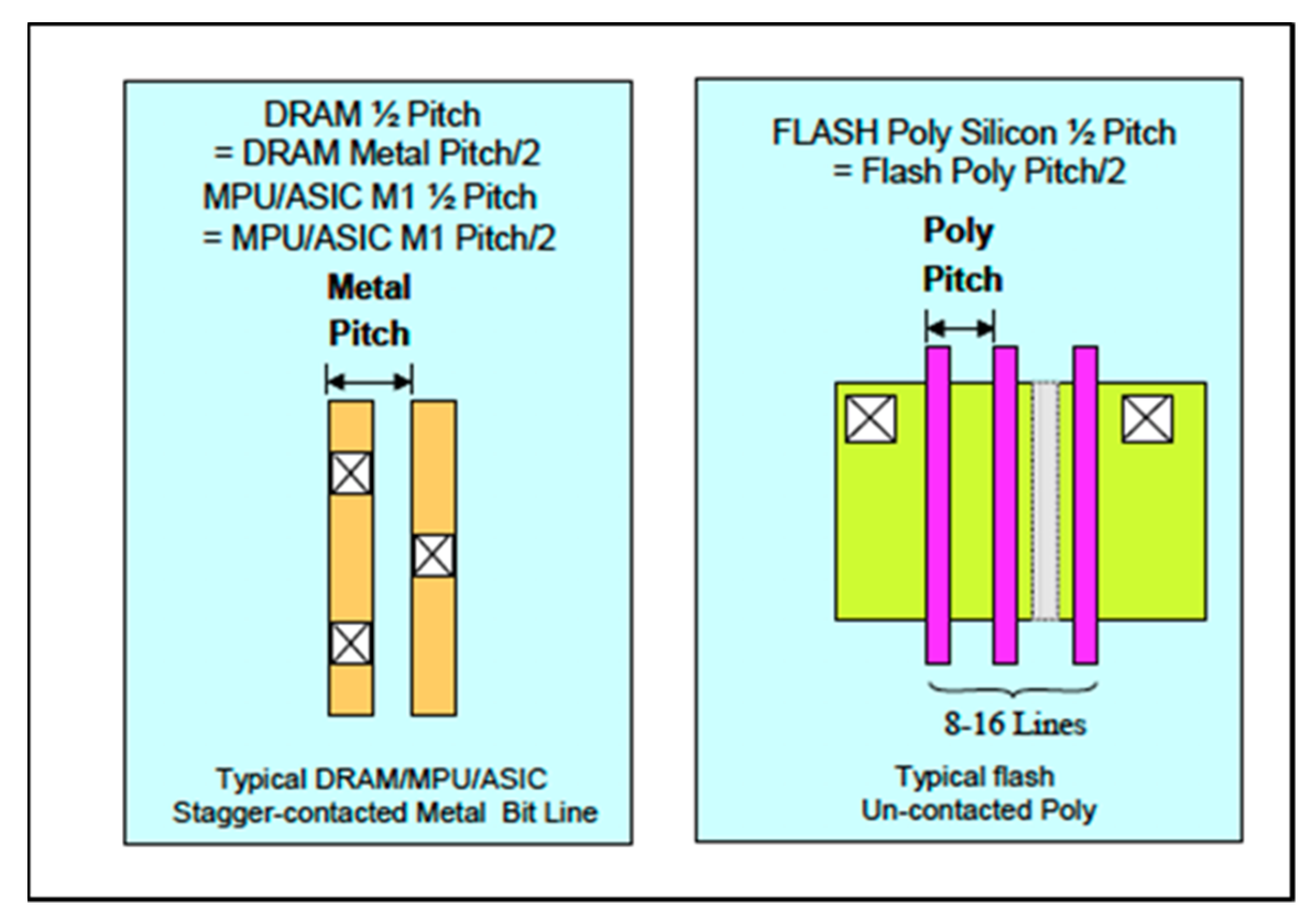
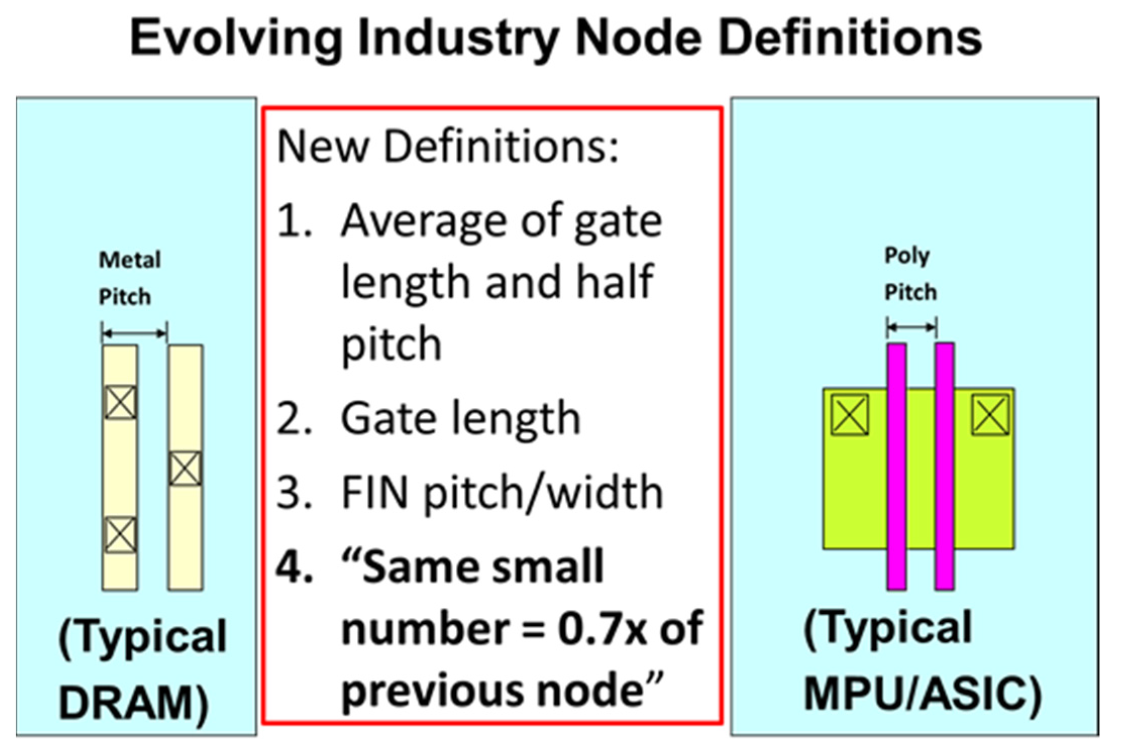
Bringing the Node Nomenclature Back to Normal
Technology nodes were previously defined from 1992 by NTRS, ITRS and IRDS by the densest metal layer to be found in any integrated circuit leading to the smallest pitch. Half pitch of the tightest metal layer was the original definition of the node (Figure 8), which was correlated to the gate length of the devices till the 1990s, leading to both density and performance with a single number. A new technology generation used dimensions of 70% of the previous one.
Since the mid-1990s, a 2-year cycle for microprocessor technologies was adopted instead of the previous 3–4 years cycle, due to the adoption of the PC by the consumers. The demands of higher performance induced a faster evolution of the gate length of the MOSFETs with a 60% reduction compared to the previous generation, and an averaging of the dimensions of the gate length and half-pitch to define the node name. Later on, some companies used only the gate length to define the technology name, and finally a 70% reduction of the node name was proposed compared with the previous generation, independently of the real physical dimensions! (See Figure 9.)
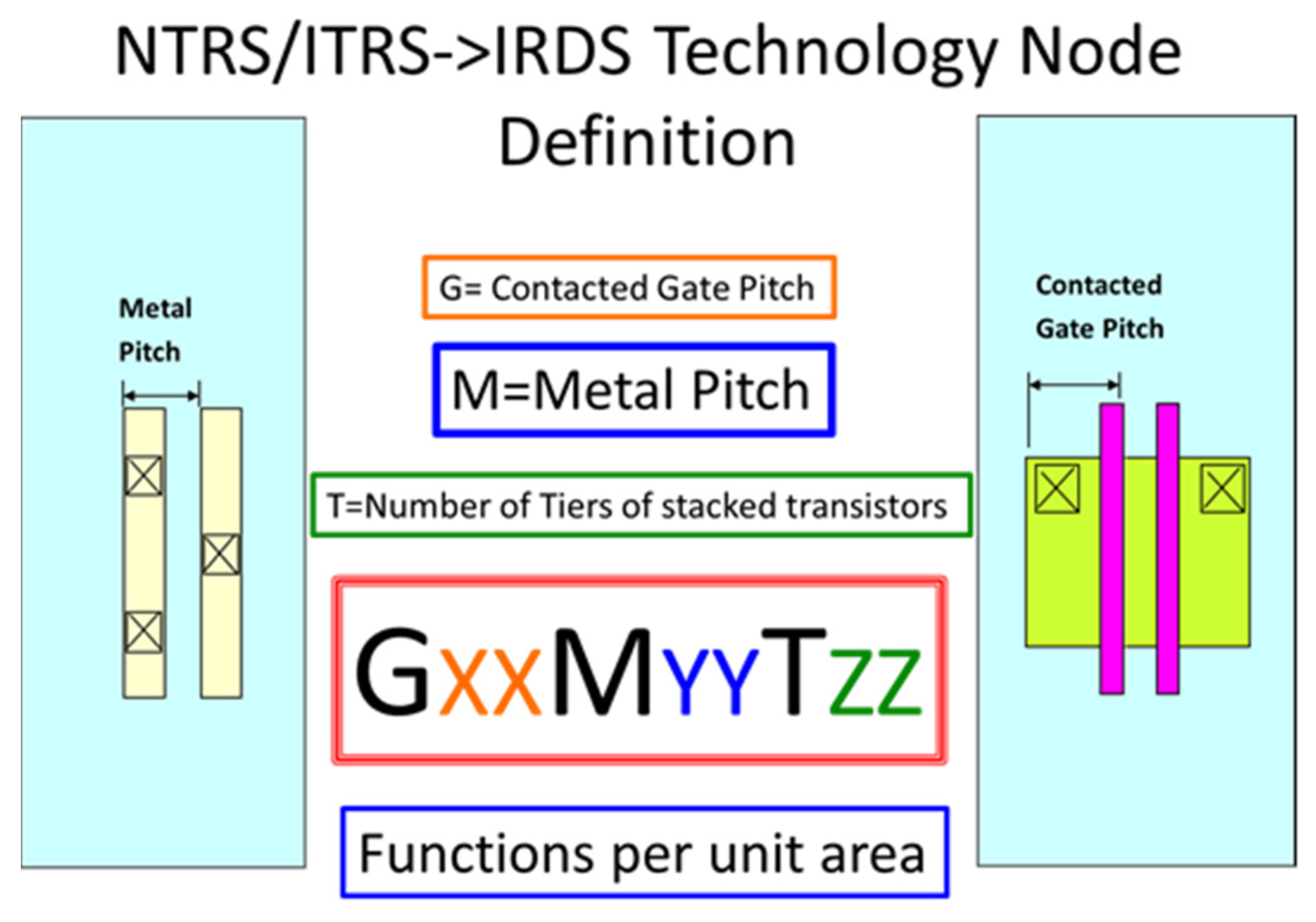
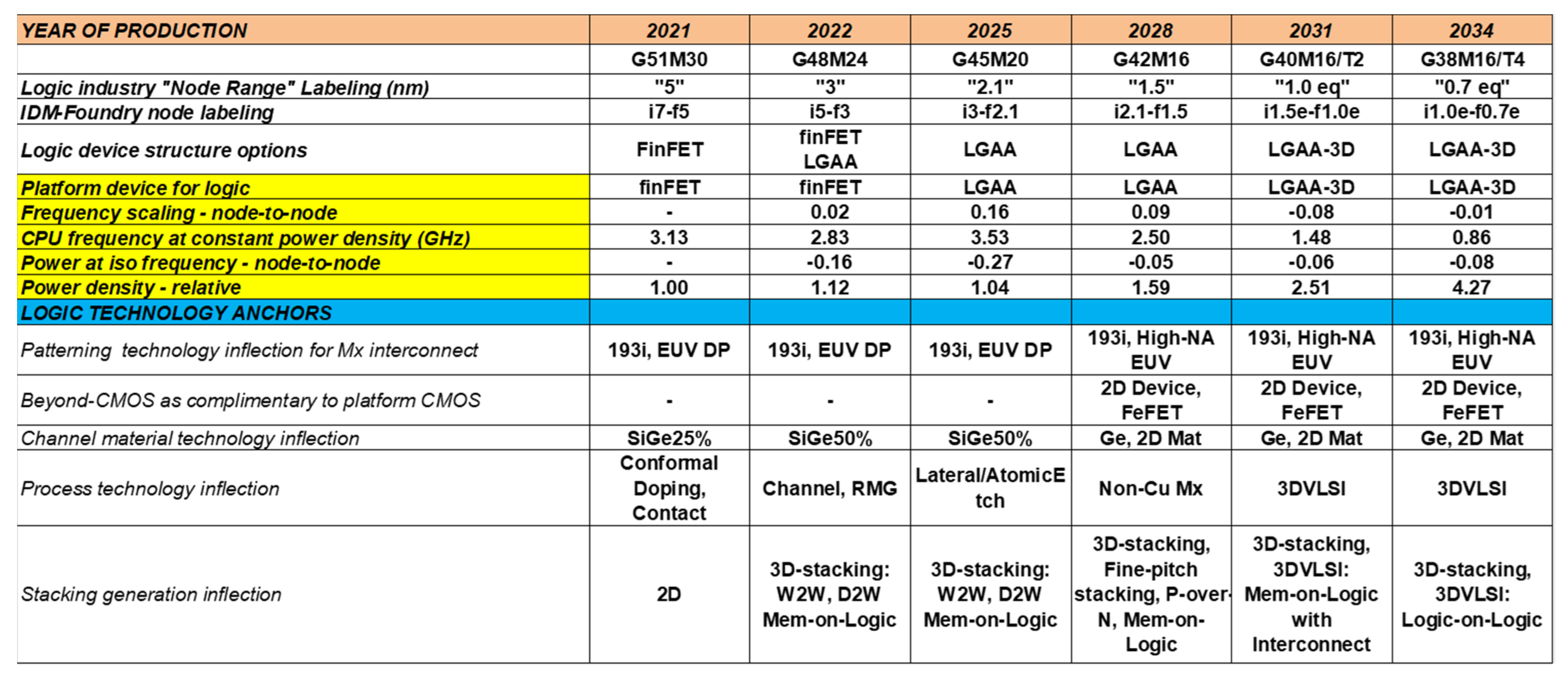
Some companies are announcing technology nodes below 1 nm by the end of this decade. In order to stay closer to the technology, the IRDS has adopted a node definition related to the NTRS and ITRS ones (Figure 10 and Figure 11).
In Figure 11, the following parameters are reported:
- -
- Top line: year for the introduction of a given technology into manufacturing;
- -
- Second line: details of the node, with G indicating the dimension of the contacted gated pitch and M the dimension of the tightest metal pitch;
- -
- Third line: “industry labeling” of technology, not correlated to reality.
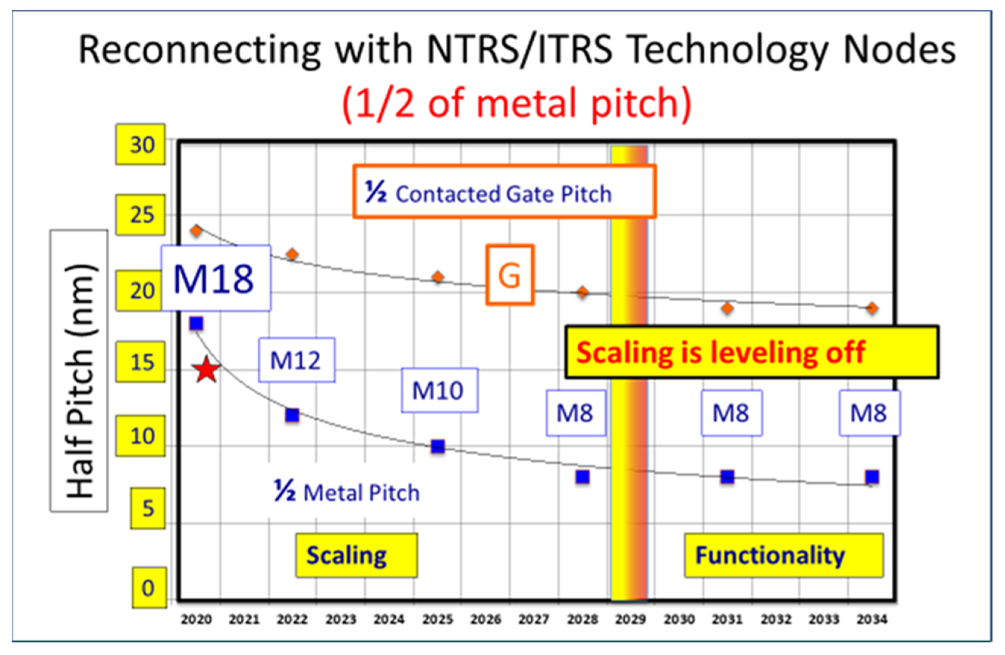
The reduction of the contacted gate pitch is used mainly for the increase of the transistor density, and does not have a great influence on the performance of ICs due to the severe power limitations mentioned above. The semiconductor industry mainly focused on the reduction of power consumption, which had become a major issue. The speed of the transistors is still progressing but not at the same rate as the one in the 1990s.
In any case, Moore’s Law and the associated scaling will continue in the next 10 years allowing for substantially increased transistor density.
However, feature scaling will reach fundamental limits in the next decade (around 7–8 nm), as shown in Figure 12, which is consistent with the prediction of the equipment industry. However, in the 2030s, other computing architectures will be able to significantly contribute to the advancement of the electronics industry.
10. 5G and Beyond Roadmap Has Become the “International Network Generations Roadmap”
The operational frequency of the cell phones started from 800–900 MHz in the 90 s with the (GSM) Global System for Mobile Communications to presently 2500–2700 MHz ranges for 4G and LTE.
In the past few years, the 5G communication infrastructure, with higher frequencies was launched. In 2017 IEEE decided to launch a new network roadmap for 5G due to the complex transition between the different communication eras. Indeed, 5G is a broad new platform covering multiple aspects of communications, including multiple bands up to the 20–40 GHz and ~60 GHZ ranges. Therefore, the roadmapping effort was named the INGR (International Network Generations Roadmap) to encompass novel network solutions. The collaboration between IRDS and INGR has been strengthened these last years.
The capabilities of ICs can cover these new frequency ranges. Different technologies, such as Wi-Fi, 4G-LTE, and communication for TV programs, developed with different market models and applications, are now contending for similar targets and solutions. Is this a recipe for some type of unification and/or consolidation among all these business models?
11. Data Centers
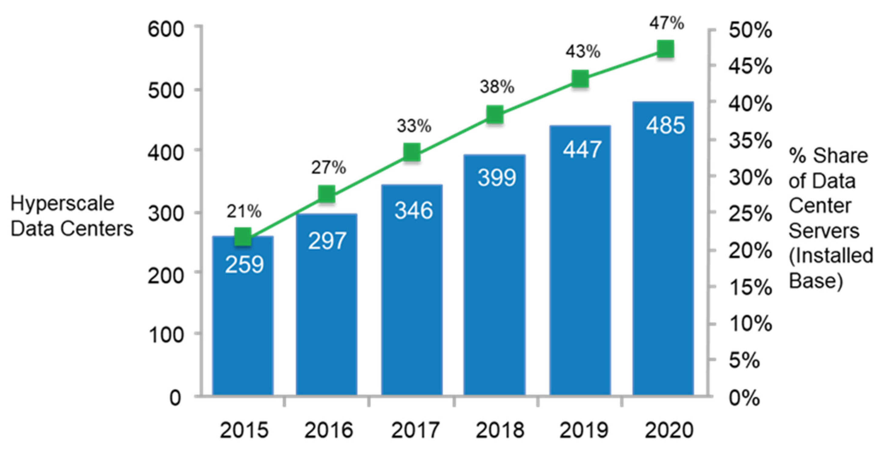
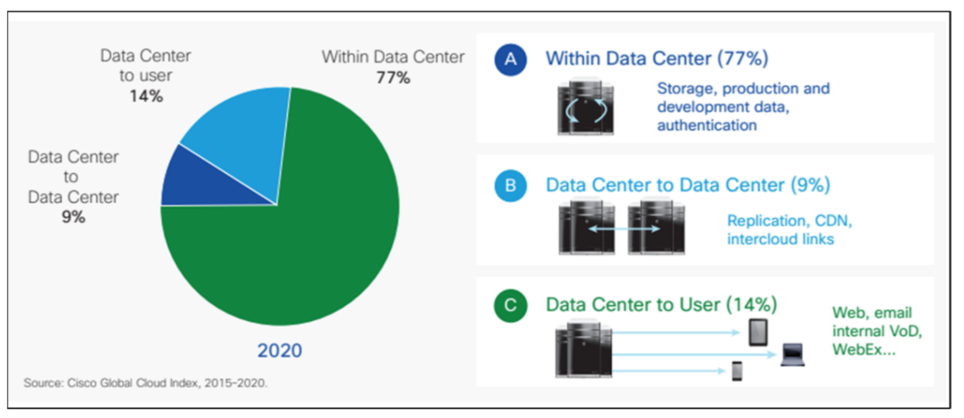
A continuous increase of gigantic clusters of servers and memory banks, called “data centers” (Figure 13), has been observed due to the exponential demand of data transfer and information. The dramatic increase of their power consumption has reached a range of hundreds of megawatts, needing complex cooling techniques. Fiber optics allow communications with low attenuation specially for long distance, but the traffic within data centers is a bottleneck (Figure 14).
The advent of multicore processors was used to “host” different operating systems in each of the cores, which was useful to address different applications leading to a substantial increase in efficiency. The data transfer in these data centers moved from 1 Gigabit Ethernet (GbE) links out of a server rack a decade ago to 100 GbE today and 400 GbE very soon, needing single mode fibers to satisfy these requirements.
12. Product Confluence and Technology Fusion
CMOS technology and derivatives is up to now at the core of many applications together with the Von Neumann architecture for the link between logic and memory. Will these technologies remain the main ones for the next decades? Indeed, substantial research efforts have been performed these last two decades for novel devices using new materials such as phase-change and resistive ones, novel physical mechanisms, such as TFETs (Tunnel FETs) and NCFETs (Negative Capacitance Ferroelectric FETs) and alternative technologies, including 3D integration, bottom-up process and alternative architectures (neuromorphic computing, quantum computing) [15,16,17,18,19,20,21,22].
Will 5G become the all-pervasive technology for cell phones, Internet devices and other applications?
It is in any case clear that devices and systems can no longer be developed independently. The electronics industry is now driven by many different products and the ITRS, which had a technology-driven bottom-up approach, had to move to the IRDS where application-driven, top-down requirements and bottom-up technology challenges are converging.
13. System Integration
We generally need multiple sub systems to be integrated in a system to satisfy the requirements for diverse functionalities, leading to possible reliability and cost issues. However, evolving technology capabilities, using monolithic or heterogeneous integration at the die level, or integration at the package level, allow one to make substantial progress that is able to overcome these challenges, the selection being made for each application.
Historically, heterogeneous integration has been launched using a printed circuit board (PCB) with an electrical connection of different electronic components using conductive tracks and pads. More recently flip chip (FC) technology associated with 2.5D tight integration, and through silicon vias (TSV) 3D stack HBM (high bandwidth memory) has become available. For example, these techniques have been used to stack the memory on top of the logic in order to reduce the computing delay, which is mainly due to the logic-memory connection.
14. More Than Moore and Packaging Integration
For smart system applications, heterogeneous integration of digital, analog and mixed-signal technologies is needed. This More than Moore (MtM) domain was firstly introduced in the framework of ITRS in 2005, then it was fully integrated in the NEREID and IRDS Roadmaps in the last decade. At the same time, the Roadmaps became mostly application driven instead of only technology driven. This new paradigm is associated with the need of multidisciplinary expertise along the complete innovation chain to develop generic technology modules, which can be made available on open technology platforms.
MtM includes innovative functionalities, in addition to logic and memory, such as RF communication [23], sensing [24], energy harvesting and management, power devices, flexible electronics. Complex embedded software needs also to be integrated into SoCs and SiPs to optimize performance scaling.
The Packaging Contribution
Several advancements in Flip Chip technologies have contributed to develop a viable and cost-effective approach. It is now used in many applications: microprocessors, low-cost GaAs power amplifiers, back-illuminated sensors (BIS) imaging chips, flat panel displays, lasers, LEDs, 3D stacked chips including logic chips and HBM memories.
All of the above systems specifications dictate the requirements for the semiconductor industry.
15. Beyond Dimensional Scaling
The combination of 3D scaling using monolithical (SoC) and heterogeneous (SiP) techniques will enable the integration of a higher density of devices in a well-defined area/volume according to Moore’s Law for the next two decades. However, physical, topological or technological limits could be reached at the end of this decade.
When overall 3D topological limitations will be reached it will not be possible to increase the number of devices in an IC; but is it possible to increase performance with a given number of devices with the same size?
An example of possible solutions is given by Flash memory products, with a storage of up to 4 bits in a single cell. Another possible solution using a multi-bit approach is given by a new way of computing: the Quantum Information Processing.
Quantum Information Processing (QIP)
Quantum computing relies on quantum bits (qubits), a qubit being a quantum-mechanical superposition of 0 and 1, which can be correlated through quantum entanglement. A massive quantum parallelism on a single quantum core can be use in the framework of this new paradigm. Quantum mechanics mainly applies at the atomic level, but it can be used in circuits based, e.g., on superconducting or spin qubits operating at very low temperatures. This new computing approach is not universal in order to solve all problems but could be exponentially more efficient for several applications. QIP is facing many challenges that have to be solved in the next decades.
Another approach utilizing more than one bit in a physical location consists of quantum annealing. This method, related to adiabatic quantum computing, is an approach in which binary variables are represented with qubits, each of which is initialized into a superposition of 0 and 1. However, hybrid cooperation with a classical computer is highly recommended.
Another class of quantum computing is the quantum gate model, using quantum logic gates to achieve a general-purpose quantum computer, creating a quantum von Neumann architecture using quantum gates instead of classical gates. Potential applications include classically challenging computational problems, such as factoring large numbers, database search, portfolio optimization, machine learning, and combinatorial optimization.
It should however be pointed out that most of the results of quantum computing calculations will often need additional data manipulation to become practically useable using classical computers.
16. Overall Roadmap Systems and Technology Characteristics (ORSC and ORTC)
The Overall Roadmap Systems Characteristics (ORSC) is given in the following Table 1, showing the main figures of merit as a function of the time horizons for very important applications: Cloud Computing, Mobile, Internet of Things, and Cyber Physical Systems.
The number of CPU or GPU cores continues to increase in the next decade. Frequency of operation will continue to increase especially for mobile systems but only moderately for other applications. However, power dissipation will remain an important challenge which needs to be taken into account.
Table 2 gives the Overall Roadmap Technology Characteristics for logic, DRAM and Flash memory devices as a function of time horizons.
17. IRDS: Summary of the International Focus Teams (IFT)
17.1. Applications Benchmarking (AB)
The aim of the AB IFT in the IRDS is the identification and periodic update of key application drivers, and to the performance of these applications as a function of the time horizons.
17.2. Systems and Architecture (SA)
A top-down, system-driven 15-year roadmapping addressing key market drivers of the semiconductor industry is performed in the SA IFT.
17.3. Outside System Connectivity (OSC)
In the OSC IFT in the IRDS the identification and assessment of capabilities needed to connect very different elements in the Internet of Everything (IoE) era is carried out together with the highlight technology needs and gaps. Applications include mobility, aerospace, home, factory, data centers and warehouses.
17.4. More Moore (MM)
The physical, electrical and reliability requirements for logic and memory technologies are at the core of the MM IFT in order to sustain More Moore applications (Power, performance, area, cost scaling for big data, mobility, cloud, IoT and server), including the transition from 2D to 3D integration.
17.5. Beyond CMOS (BC)
The mission of the BC IFT is to survey and assess the most promising future information processing technologies, which could be useful to overcome some CMOS limits, for instance in the field of power consumption.
17.6. Cryogenics Electronics and Quantum Information Processing (CE&QIP)
The catalog and evaluation of CEQUIP technologies is the goal of this IFT. It assesses the status of technologies in the areas of low temperature electronics and quantum information processing. It covers cryogenic electronics for temperature below −150 °C, including semiconductor and superconductor devices. On the other hand, quantum information processing using qubits is also addressed in this chapter.
17.7. Packaging Integration (PI)
This IFT is devoted to packaging integration, which is the last manufacturing process for functional products. Packaging includes electrical connections for signal transmission, power input and voltage control. It also aims to overcome thermal dissipation and reliability issues.
17.8. Factory Integration (FI)
The focus of factory Integration focus is to ensure that the semiconductor-manufacturing infrastructure is able to produce items at affordable cost and high volume. This includes yield improvement to near 100% and wafer size increases.
17.9. Lithography (L)
The Lithography IFT focuses on patterning technology for the production of high-performance logic, DRAM, and Flash chips. EUV (Extreme Ultraviolet Lithography) is now the leading-edge technique thanks to the reduction of the development cycle and manufacturing cycle times, the decrease of the numbers of patterning levels and overall complexity.
17.10. Yield Enhancement (YE)
The Yield Enhancement is devoted to the optimization of the semiconductor manufacturing. The production of the maximum number of functional units if at the center of the YE IFT. Avoiding defects, contamination and variability is the main goal of the manufacturing techniques.
17.11. Metrology (M)
Emerging measurement challenges from devices, systems, and integration is the main mission of the metrology IFT. This chapter covers CMOS, beyond CMOS, communication devices, More than Moore devices, materials and structures, as well as process control and failure analysis.
17.12. Environment, Safety, Health, and Sustainability (ESH/S)
The ESH/S IFT addresses critical Environment, Safety, Health and Sustainability challenges for future manufacturing technologies and identifies key new markets and opportunities.
17.13. More Than Moore (MtM)
The MtM chapter of the IRDS covers non-digital functionalities that do not necessarily scale according to Moore’s Law, which are needed for future smart electronics nano-systems, It includes sensors, actuators, energy harvesting and management, flexible electronics and power devices.
18. Conclusions
In this paper the international effort to map the future of nanoelectronics from materials to systems for the new electronics industry has been presented.
The following sections have been highlighted: the Roadmap structure with the international teams, the methodology and historical evolution, the various eras of scaling, the new ecosystems and computer industry, the evolving supply chain, the development of SoC and SiP, the advent of the Internet of Everything and the 5G communications, the dramatic increase of data centers, the power challenge, the technology fusion, heterogeneous and system integration, the emerging technologies, devices and computing architectures, and the main challenges for future applications.
Funding
This research received no external funding.
Institutional Review Board Statement
Not applicable.
Acknowledgments
The content of this article is based on 2020IRDS publications. The authors would like to thank all the IRDS teams.
Conflicts of Interest
The authors declare no conflict of interest.
References
- Available online: https://www.sdrj.jp/ (accessed on 2 June 2021).
- Available online: https://www.nereid-h2020.eu/ (accessed on 3 June 2019).
- Available online: https://0-irds-ieee-org.brum.beds.ac.uk/ (accessed on 1 December 2020).
- Available online: https://www.sinano.eu/ (accessed on 2 June 2021).
- Moore, G.E. Cramming more components onto integrated circuits. Electronics 1965, 38, 114. [Google Scholar] [CrossRef]
- Moore, G.E. Progress in digital integrated circuits. In Proceedings of the Plenary Address, International Electron Devices Conference, Washington, DC, USA, 1–3 December 1975. [Google Scholar]
- Dennard, R.H.; Gaensslen, F.H.; Yu, H.N.; Rideout, V.L.; Bassous, E.; LeBlanc, A.R. Design of ion-implanted MOSFET’s with very small physical dimensions. IEEE J. Solid State Circuits 1974, 9, 256–268. [Google Scholar] [CrossRef] [Green Version]
- Welser, I.; Hoyt, J.L.; Gibbons, J.F. Electron mobility enhancement in strained Si n-type MOSFET. IEEE Electron Device Lett. 1994, 15, 100–102. [Google Scholar] [CrossRef]
- Hoyt, J.L.; Nayfeh, H.M.; Eguchi, S.; Aberg, I.; Xia, G.; Drake, T.; Fitzgerald, E.A.; Antoniadis, D.A. Strained silicon MOSFET technology. In Proceedings of the Digest International Electron Devices Meeting, San Francisco, CA, USA, 8–11 December 2002. [Google Scholar] [CrossRef]
- Cheng, B.; Cao, M.; Rao, R.; Inani, A.; Voorde, P.V.; Greene, W.M.; Stork, J.M.C.; Yu, Z.; Zeitzoff, P.M.; Woo, J.C.S. The impact of high-κ gate dielectrics and metal gate electrodes on sub-100 nm MOSFETs. IEEE Tran. Electron. Dev. 1999, 46, 1537–1544. [Google Scholar] [CrossRef]
- Pfiester, J.R.; Sivan, R.D.; Liaw, H.M.; Seelbach, C.A.; Gunderson, C.D. A self-aligned elevated source/drain MOSFET. IEEE Electron Device Lett. 1990, 11, 365–367. [Google Scholar] [CrossRef]
- Balestra, F.; Cristoloveanu, S.; Benachir, M.; Brini, J.; Elewa, T. Double-gate Silicon-On-Insulator transistor with volume inversion: A new device with greatly enhanced performance. IEEE Electron Device Lett. 1987, 8, 410–412. [Google Scholar] [CrossRef]
- Yeap, G.; Lin, S.S.; Chen, Y.M.; Shang, H.L.; Wang, P.W.; Lin, H.C.; Peng, Y.C.; Sheu, J.Y.; Wang, M.; Chen, X.; et al. 5 nm CMOS production technology platform featuring full-fledged EUV, and high mobility channel FinFETs with densest 0.021 um2 SRAM cells for mobile SoC and high performance computing applications. In Proceedings of the 2019 IEEE International Electron Devices Meeting (IEDM), San Francisco, CA, USA, 7–11 December 2019. [Google Scholar]
- Bae, G.; Bae, D.I.; Kang, M.; Hwang, S.M.; Kim, S.S.; Seo, B.; Kwon, T.Y.; Lee, T.J.; Moon, C.; Choi, Y.M.; et al. 3 nm GAA technology featuring multi-bridge-channel FET for low power and high performance applications. In Proceedings of the 2018 IEEE International Electron Devices Meeting (IEDM), San Francisco, CA, USA, 1–5 December 2018. [Google Scholar]
- Khosla, R.; Sharma, S.K. Integration of ferroelectric materials: An ultimate solution for next-generation computing and storage devices. ACS Appl. Electron. Mater. 2021, 3, 2862–2897. [Google Scholar] [CrossRef]
- Salahuddin, S.; Datta, S. Use of negative capacitance to provide voltage amplification for low power nanoscale devices. Nano Lett. 2008, 8, 405–410. [Google Scholar] [CrossRef] [PubMed]
- Nikonov, D.E.; Young, I.A. Benchmarking of beyond-CMOS exploratory devices for logic integrated circuits. IEEE J. Explor. Solid-State Comput. Devices Circuits 2015, 1, 3–11. [Google Scholar] [CrossRef]
- Chen, A. A review of emerging Non-Volatile Memory (NVM) technologies and applications. Solid-State Electron. 2016, 125, 25–38. [Google Scholar] [CrossRef]
- Batude, P.; Ernst, T.; Arcamone, J.; Arndt, G.; Coudrain, P.; Gaillardon, P.E. 3-D sequential integration: A key enabling technology for heterogeneous co-integration of new function with CMOS. J. Emerg. Sel. Top. Circuits Syst. 2012, 2, 714–722. [Google Scholar] [CrossRef]
- Rachmady, W.; Agrawal, A.; Sung, S.H.; Dewey, G.; Chouksey, S.; Chu-Kung, B.; Elbaz, G.; Fischer, P.; Huang, C.Y.; Jun, K.; et al. 300mm heterogeneous 3D integration of record performance layer transfer germanium PMOS with silicon NMOS for low power high performance logic applications. In Proceedings of the 2019 IEEE International Electron Devices Meeting (IEDM), San Francisco, CA, USA, 7–11 December 2019. [Google Scholar]
- Chien, W.C.; Cheng, H.Y.; BrightSky, M.; Ray, A.; Yeh, C.W.; Kim, W.; Bruce, R.; Zhu, Y.; Ho, H.Y.; Lung, H.L.; et al. Reliability study of a 128Mb phase change memory chip implemented with doped Ga-Sb-Ge with extraordinary thermal stability. In Proceedings of the 2016 IEEE International Electron Devices Meeting (IEDM), San Francisco, CA, USA, 3–7 December 2016. [Google Scholar]
- Chen, H.Y.; Yu, S.; Gao, B.; Huang, P.; Kang, J.; Wong, H.S.P. HfOx based vertical resistive random-access memory for cost-effective 3D cross-point architecture without cell selector. In Proceedings of the 2012 International Electron Devices Meeting, San Francisco, CA, USA, 10–13 December 2012; pp. 20–27. [Google Scholar]
- Carter, R.; Mazurier, J.; Pirro, L.; Sachse, J.U.; Baars, P.; Faul, J.; Grass, C.; Grasshoff, G.; Javorka, P.; Kammler, T.; et al. 22 nm FDSOI technology for emerging mobile, internet-of-things, and RF applications. In Proceedings of the 2016 IEEE International Electron Devices Meeting (IEDM), San Francisco, CA, USA, 3–7 December 2016. [Google Scholar]
- Ouerghi, I.; Philippe, J.; Duraffourg, L.; Laurent, L.; Testini, A.; Benedetto, K.; Charvet, A.M.; Delaye, V.; Masarotto, L.; Scheiblin, P.; et al. High performance polysilicon nanowire NEMS for CMOS embedded nanosensors. In Proceedings of the 2014 IEEE International Electron Devices Meeting, San Francisco, CA, USA, 15–17 December 2014. [Google Scholar]
Figure 1.
Development of multicore architecture in the first decade of this century (source, accessed on 1 July 2016: https://developer.ibm.com/articles/j-java-streams-4-brian-goetz/).
Figure 1.
Development of multicore architecture in the first decade of this century (source, accessed on 1 July 2016: https://developer.ibm.com/articles/j-java-streams-4-brian-goetz/).

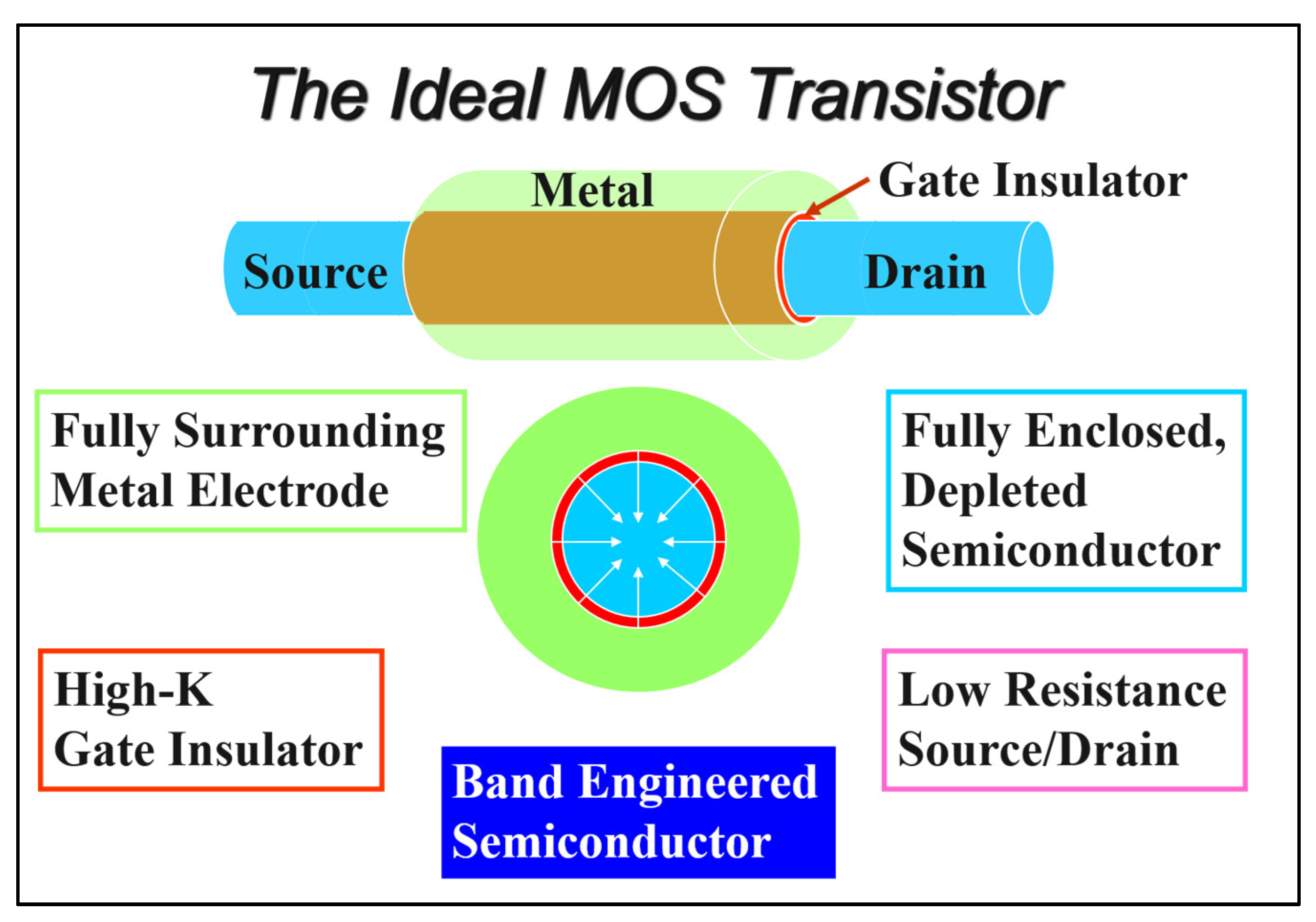
Figure 2.
The vision of innovative MOS transistor.

Figure 3.
From major innovation to implementation in high-volume: Strained Silicon [8,9], High k/Metal Gate [10], Raised Source/Drain [11], Multi-Gates [12].

Figure 4.
The past extrapolation showing that 2D scaling faced fundamental limits beyond 2020.

Figure 5.
Flash memory launched 3D scaling in 2014 (source, accessed on 1 August 2015: https://www.samsung.com/semiconductor/global.semi.static/2bit_V-NAND_technology_White_Paper-1.pdf).
Figure 5.
Flash memory launched 3D scaling in 2014 (source, accessed on 1 August 2015: https://www.samsung.com/semiconductor/global.semi.static/2bit_V-NAND_technology_White_Paper-1.pdf).

Figure 6.
The 3 eras of transistor scaling highlighted by NTRS, ITRS, ITRS 2.0, IRDS.

Figure 7.
Source: Statista, Sales of smartphones saturated in 2017 then declined in 2020 (* forecast).
Figure 7.
Source: Statista, Sales of smartphones saturated in 2017 then declined in 2020 (* forecast).

Figure 8.
Technology node definition used by the previous Roadmaps.

Figure 9.
Evolution of technology node definition used by industry.

Figure 10.
Technology node adopted by IRDS.

Figure 11.
IRDS Roadmap for the next years. Notes: Mx—Tight-pitch routing metal interconnect, IDM—integrated device manufacturer, FinFET—fin field-effect transistor, LGAA—lateral gate all around, EUV—extreme ultraviolet, NA—numerical aperture, Ge—germanium, SiGe—silicon germanium. RMG—replacement metal gate, VLSI—very large-scale integration, W2W—wafer to wafer, D2W—die to wafer, Mem-on-Logic—memory on logic.

Figure 12.
Metal pitch and contacted gate pitch scaling vs. time horizons.

Figure 13.
The number of data centers is accelerating (source: Cisco Global Cloud Index, 2015–2020, Synergy Research).
Figure 13.
The number of data centers is accelerating (source: Cisco Global Cloud Index, 2015–2020, Synergy Research).

Figure 14.
Traffic within data center is the bottleneck (source: Cisco Global Cloud Index, 2015–2020).
Figure 14.
Traffic within data center is the bottleneck (source: Cisco Global Cloud Index, 2015–2020).


Table 1.
Overall Roadmap System Characteristics for the different applications (in yellow: 5G maximum data rate).
Table 1.
Overall Roadmap System Characteristics for the different applications (in yellow: 5G maximum data rate).
| 2020 IRDS Driver (Exec Summary) Prep—ORSC | |||||||
|---|---|---|---|---|---|---|---|
| YEAR OF INTRODUCTION | 2019 | 2020 | 2022 | 2025 | 2028 | 2031 | 2034 |
| Cloud Computing (CC) | |||||||
| # Cores per Socket | 38 | 42 | 50 | 62 | 70 | 70 | 70 |
| Processor Base Frequency (for multiple cores together) | 3.00 | 3.10 | 3.30 | 3.60 | 3.90 | 4.20 | 4.5 |
| L1 Data Cache Size (in KB) | 36 | 38 | 40 | 42 | 44 | 44 | 44 |
| L1 Instruction Cache Size (in KB) | 48 | 64 | 96 | 128 | 160 | 160 | 160 |
| HBM Bandwidth (TB/s) | 2.4 | 2.4 | 6 | 6.6 | 6.6 | 6.6 | 6.6 |
| Into-Out of Server Data Rate/lane (Gb/s) (Package) | 56 | 56 | 56 | 56 | 56 | 100 | 100 |
| Socket TDP (Watts) | 226 | 237 | 262 | 303 | 351 | 387 | 425 |
| SA Mobile Table—Focus Drivers Line Items | |||||||
| # CPU cores | 10 | 10 | 12 | 18 | 25 | 28 | 30 |
| # GPU cores | 16 | 32 | 32 | 64 | 128 | 256 | 512 |
| Max Freq (GHz) | 2.8 | 3.0 | 3.7 | 4.9 | 6.5 | 8.6 | 11.5 |
| Cellular Data rate (Mb/s) | 22 | 22 | 1000 | 1000 | 1000 | 1000 | 1000 |
| 5G Maximum Data Rate (Gb/s) | 1 | 5 | 5 | 7 | 10 | 20 | 50 |
| # Sensors | 6 | 8 | 10 | 12 | 12 | 16 | 16 |
| Board Power (mW) | 5096 | 5351 | 5899 | 6829 | 7906 | 9152 | 10594 |
| SA IoT Table—Focus Drivers Line Items | |||||||
| CPUs per device | 1 | 2 | 2 | 4 | 6 | 8 | 8 |
| Max CPU Frequency (MHz) | 277 | 300 | 310 | 325 | 341 | 357 | 375 |
| Energy Source (B = battery, H = energy harvesting) | B + H | B + H | B + H | B + H | B + H | B + H | B + H |
| Sensors per device | 4 | 4 | 8 | 12 | 16 | 16 | 16 |
| SA CPS Table—Focus Drivers Line Items | |||||||
| Number of Devices | 64 | 64 | 64 | 128 | 256 | 512 | 512 |
| CPUs per Device | 4 | 4 | 8 | 12 | 12 | 16 | 16 |
Table 2.
Overall Roadmap Technology Characteristics.
| 2020 IRDS Executive Summary Drivers—ORTC | ||||||||
|---|---|---|---|---|---|---|---|---|
| YEAR OF PRODUCTION | 2019 | 2020 | 2022 | 2025 | 2028 | 2031 | 2032 | 2034 |
| Logic device technology naming: NEW node defintion | G54M38 | G48M36 | G45M24 | G45M20 | G40M16 | G38M16T2 | G38M16T3 | G38M16T4 |
| Logic industry “Node Range” Labeling (nm) | “7” | “5” | “3” | “2.1” | “1.5” | “1.0 nm eq” | “1.0 nm eq” | “0.7 nm eq” |
| Logic device structure options | FinFET | FinFET | FinFET LGAA | LGAA | LGAA VGAA | LGAA-3D VGAA | LGAA-3D VGAA | LGAA-3D VGAA |
| LOGIC CELL AND FUNCTIONAL FABRIC TARGETS | ||||||||
| Average Cell Width Scaling Factor Multiplier | 1 | 0.9 | 0.9 | 0.9 | 0.9 | 0.9 | 0.9 | 0.9 |
| LOGIC DEVICE GROUND RULES | ||||||||
| MPU/Soc M0 ½ Pitch (nm) | 18 | 15 | 12 | 10.5 | 8 | 8 | 8 | 8 |
| Physical Gate Length for HP Logic (nm) | 20 | 18 | 16 | 14 | 12 | 12 | 12 | 12 |
| Lateral GAA (nanosheet) Minimum Thickness (nm) | ||||||||
| Minimum Device Width (FinFET fin, nanosheet, SRAM) or Diameter (nm) | 9 | 7 | 6 | 7 | 6 | 6 | 6 | 6 |
| LOGIC DEVICE Electrial | ||||||||
| Vdd (V) | 0.75 | 0.7 | 0.7 | 0.65 | 0.65 | 0.6 | 0.6 | 0.6 |
| DRAM TECHNOLOGY | ||||||||
| DRAM Min half piutch (nm) | 18 | 17.5 | 17 | 14 | 11 | 8.4 | 8.4 | 7.7 |
| DRAM Min Hal Plich (Calculatod Half plich) (nm) | 20.5 | 17.5 | 18.5 | 15 | 12 | 10 | 10 | 8.5 |
| DRAM Coll slzo Factor: aF^2 | 6 | 6 | 4 | 4 | 4 | 4 | 4 | 4 |
| DRAM Gb/1chip target | 8 | 8 | 16 | 16 | 32 | 32 | 32 | 32 |
| NAND Flash | ||||||||
| Flash 2D NAND Flash unconfacted poly 1/2 pitch-F(nm)2D | 15 | 15 | 15 | 15 | 15 | 15 | 15 | 15 |
| Flash Product highost densilty (indpendent of 2D or 3D) | 512G | 1T | 1T | 1.5T | 3T | 4T | 4T | 4T+ |
| Flash Product Maximum btell (2D_3D) | 2_4 | 2_4 | 2_4 | 2_4 | 2_4 | 2_4 | 2_4 | 2_4 |
| Flash 3D NAND Maximum Number or Momoy Layers | 48–65 | 64–96 | 96–128 | 128–192 | 256–384 | 384–512 | 384–512 | 512+ |
Publisher’s Note: MDPI stays neutral with regard to jurisdictional claims in published maps and institutional affiliations. |
© 2021 by the authors. Licensee MDPI, Basel, Switzerland. This article is an open access article distributed under the terms and conditions of the Creative Commons Attribution (CC BY) license (https://creativecommons.org/licenses/by/4.0/).
Share and Cite
MDPI and ACS Style
Gargini, P.; Balestra, F.; Hayashi, Y. Roadmapping of Nanoelectronics for the New Electronics Industry. Appl. Sci. 2022, 12, 308. https://0-doi-org.brum.beds.ac.uk/10.3390/app12010308
AMA Style
Gargini P, Balestra F, Hayashi Y. Roadmapping of Nanoelectronics for the New Electronics Industry. Applied Sciences. 2022; 12(1):308. https://0-doi-org.brum.beds.ac.uk/10.3390/app12010308
Chicago/Turabian StyleGargini, Paolo, Francis Balestra, and Yoshihiro Hayashi. 2022. "Roadmapping of Nanoelectronics for the New Electronics Industry" Applied Sciences 12, no. 1: 308. https://0-doi-org.brum.beds.ac.uk/10.3390/app12010308
Note that from the first issue of 2016, this journal uses article numbers instead of page numbers. See further details here.