Article

Simulation Study of Vertical p–n Junction Photodiodes’ Optical Performance According to CMOS Technology

by
Gabriel M. Ferreira
1,2,
Vítor Silva
1,2,3,
Graça Minas
1,2,* and
Susana O. Catarino
1,2
1
Microelectromechanical Systems Research Unit (CMEMS-UMinho), School of Engineering, Campus de Azurém, University of Minho, 4800-058 Guimaraes, Portugal
2
LABBELS—Associate Laboratory, 4800-122 Braga, Portugal
3
INL—International Iberian Nanotechnology Laboratory, 4715-330 Braga, Portugal
*
Author to whom correspondence should be addressed.
Submission received: 7 February 2022 / Revised: 26 February 2022 / Accepted: 28 February 2022 / Published: 2 March 2022
(This article belongs to the Special Issue Novel Technology and Applications of Micro/Nano Devices and System)

Abstract

:
CMOS photodiodes have been widely reported in microsystem applications. This article presents the design and numerical simulation of p–n junction photodiodes, using COMSOL Multiphysics, for three CMOS technologies (0.18 μm, 0.35 μm and 0.7 μm) and three different p–n junction structures: n+/p-substrate, p+/n-well and n-well/p-substrate. For these simulations, the depth junctions and dopant concentrations were set according to the different technologies. Then, each photodiode was spectrophotometrically characterized regarding the current, responsivity and quantum efficiency. The obtained numerical results show that the 0.18 and 0.35 μm CMOS technologies are those with the highest peak of efficiency when visible spectral ranges are needed, comparative to the 0.7 µm technology. Furthermore, the three most common p–n vertical junction photodiode structures were compared. The n+/p-substrate junction photodiode appears to be the one with the highest quantum efficiency in the visible range, which is in agreement with the literature. It can be concluded that the photodiodes’ characteristic curves and dark current values are consistent with reports in the literature. Therefore, this numerical approach allows to predict the photodiodes’ performance, helping to select the best structural design for each required application, before their microfabrication.

1. Introduction

Photodetectors are optical sensors that are increasing in importance, mainly due to their high ability for being miniaturized and on-chip integrated, in several devices for different application areas [1,2]. In particular, photodiodes are optical sensors that convert light intensity into a photocurrent. Their operation principle is based on the photoelectric effect, where photons are converted into electron-hole pairs [3]. Photodiodes are typically characterized based on their generated current, dark current, responsivity and quantum efficiency features. The responsivity R (A/W) indicates the photodiode’s ability to absorb incident light, relating the produced current (Iph) to the incident optical power (Pin), as given by (1). The quantum efficiency ( φ ) describes the fraction of the incident optical power that contributes to the generated photocurrent, and it is given by (2), where h corresponds to the Plank constant (h = 6.6261 × 10 34   J · s ) , f is the incident frequency (Hz) and q the electron charge (q = 1. 6 × 10 19 C).
R = I p h P i n
φ = R × h × f q
Photodiodes can be microfabricated using Complementary Metal Oxide Semiconductor (CMOS) technology, which has enabled a major technological advance in the manufacturing of integrated sensors (namely optical sensitive surfaces), circuits and microchips in the last decades [3,4]. The reduction of the power consumption, the increase in the integration capacity and the low cost are strengths of CMOS technology, playing a key role in the most diverse areas of technology [5]. Over the years, CMOS has been the main competitor of CCD (Charge Couple Device) technology in the manufacturing of photodetectors. Although CCD is usually associated with higher quality images (due to their superior fill factor, when compared to the first CMOS devices), it is characterized by a high-power consumption and a large area per cell [6,7], when compared to CMOS technology. However, despite CMOS technology being more susceptible to noise, their low-power consumption is an advantage for portable and miniaturized devices. Additionally, back-illuminated CMOS photodiode sensors present improvements in the signal-to-noise ratio and in the fill factor, being able to compete with the CCD photodetectors in these features [8]. In addition to these features, CMOS active pixel sensors have also improved the speed and the signal-to-noise ratio of the CMOS sensors, despite having an even lower fill factor than the CCD detectors [9]. Moreover, CMOS photodetectors can be produced in the same substrate and same chip as their readout electronics. However, when compared to bipolar and other technologies used in microelectronics, CMOS technology has also some limitations. Unlike bipolar technology [5,7], CMOS manufacturing is more susceptible to contamination, due to the shallow diffusion on the silicon substrate and, therefore, even a small dust particle could compromise the entire process [5]. More recently, another technology has emerged, BiCMOS (or bipolar CMOS), to address the disadvantages presented by the CMOS and the bipolar technology. However, it presents a substantially higher cost by comparison, which makes it unfavorable for low cost and affordable processes and devices [7].
In this work, different CMOS vertical p–n junction photodiodes are studied, designed, simulated and compared for optical features. Besides the different designs of the photodiodes’ p–n junctions, which will be further detailed, it is expected that, for the same p–n junction structure, their optical response also varies according to the used CMOS technology. Therefore, herein three CMOS technologies: the 0.18 µm, the 0.35 µm and the 0.7 µm, are used for those studies. These values correspond to the minimum gate width of the metal–oxide–semiconductor field-effect transistors (MOSFETs) feasible by each technology. Besides this width, these three technologies differ also in the junctions’ depth and dopant concentration, as well as in the dimensions of contacts, metals and vias. The smaller the technology, the smaller and more compact the circuit [10].
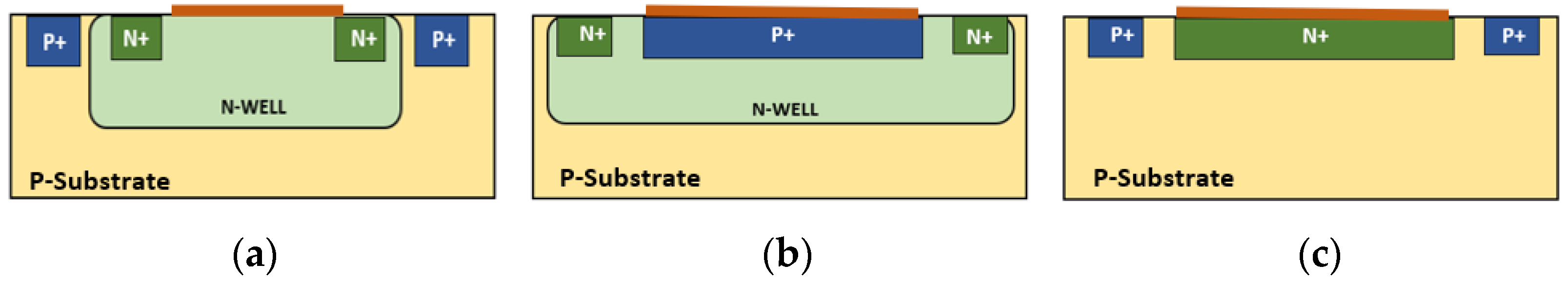
The three different types of available CMOS vertical photodiodes’ p–n junctions are based on n+/p-substrate; p+/n-well and n-well/p-substrate [7,11] as illustrated in 
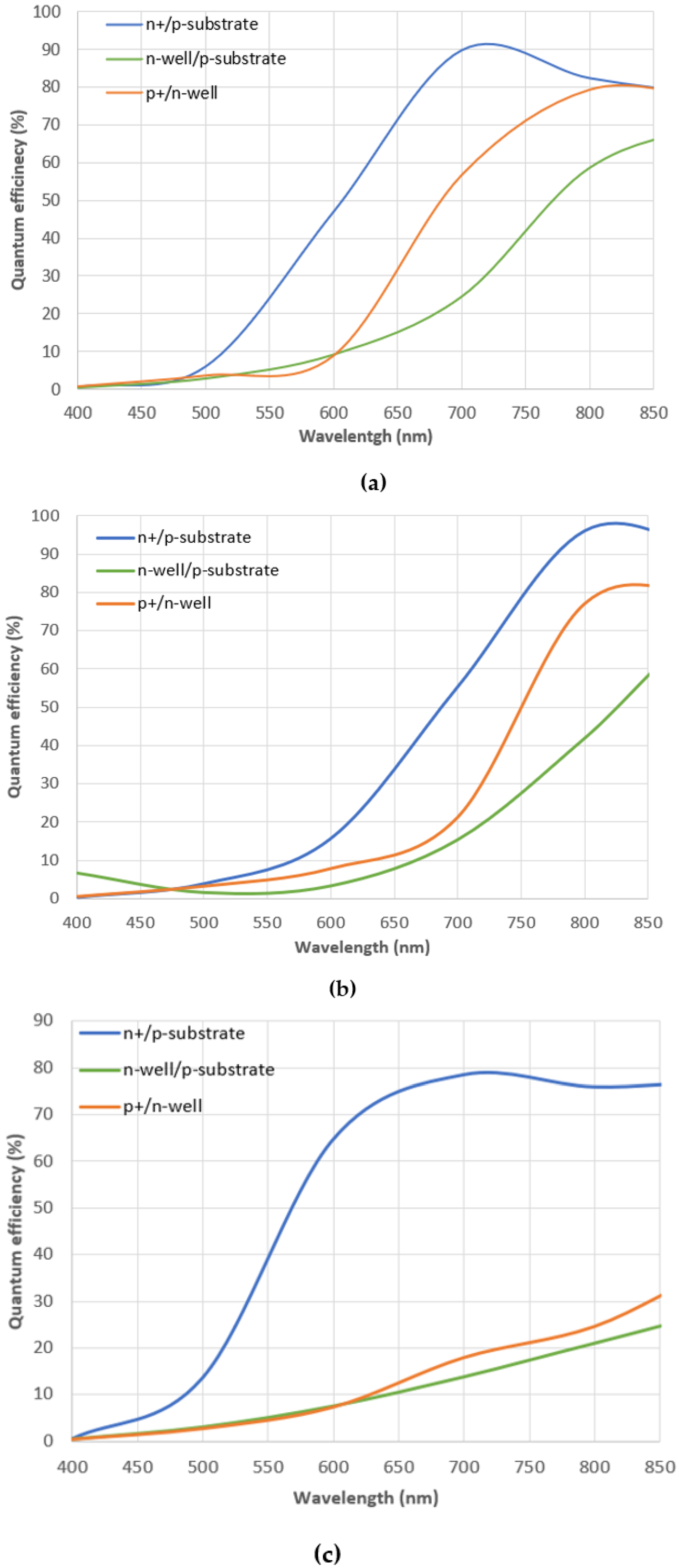
Figure 1. Due to the different junctions’ depths of these structures, according to the literature [7,
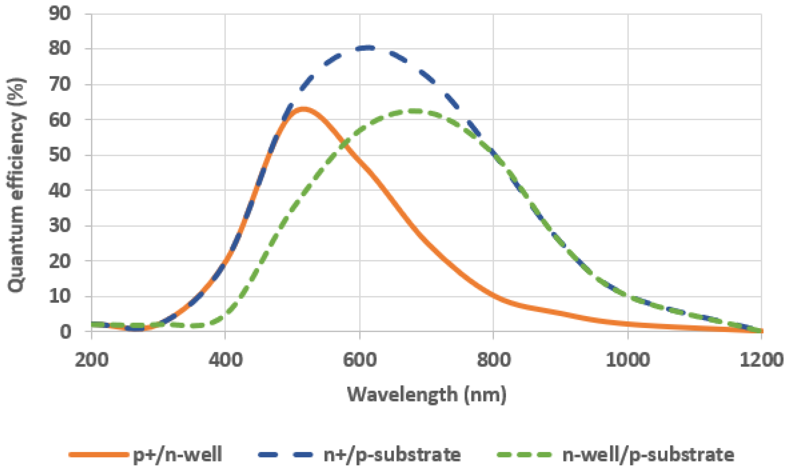
12], it is expected that their photodiodes present different quantum efficiency spectra, as shown in the example of Figure 2 (data obtained from the results of 2 µm CMOS technology photodiodes reported in literature). This occurs since the penetration depth of the light in silicon is wavelength dependent, due to the wavelength dependency of the silicon absorption coefficient in the visible spectrum [7,12]. Therefore, a shallow junction (as the n+/p-substrate or p+/n-well) collects the lower wavelengths more efficiently [7,12]. Additionally, the higher efficiency presented by the n+/p-substrate, above the 500 nm, is related to the different doping concentrations between the n and the p sides, which extends the p side depletion area more deeply.
According to the literature report of Figure 2, with an example in 2 μm technology, it is expected that the n+/p-substrate photodiode presents higher quantum efficiency than the p+/n-well and n-well/p-substrate photodiodes [7,11]. Therefore, to understand if such behavior also happens for the 0.18, 0.35 and 0.7 µm CMOS technologies, this manuscript aims to model and numerically characterize the three types of photodiodes’ junctions presented in Figure 1, for those three CMOS technologies. This will evaluate, for each structure, the differences in the optical performance, according to the manufacturing technology.
The theory regarding optical detectors is well studied and there are many reports detailing the analytical solution of the problems. However, there is a lack of literature regarding numerical methods dealing with optical–semiconductor interfaces. Thus, this work intends to overcome this gap and explore the possibility of using a finite elements’ numerical tool, in particular COMSOL Multiphysics, to understand the behavior of photodiodes in the entire optical spectrum. To the best of the authors’ knowledge, there is no other work providing this numerical comparison in the literature in the junction photodiode’s performance using different CMOS technologies for the three different types of photodiodes’ p–n junctions using the 0.18 µm, 0.35 µm and 0.7 µm CMOS technologies; this work thus fills a research void. Finally, the authors also detail the layout of the photodetectors, designed with CADENCE tools, using the 0.18 µm technology and chosen due to the better performance, including the optical response, achieved even when high frequency electronic circuits are used, since the authors intend to further integrate such photodiodes, their readout electronics and also acoustic sensors in the same CMOS chip for multisensing detection [13].

2. Methods

2.1. Numerical Simulation

COMSOL Multiphysics software, version 5.3, based on finite element analysis, was used to perform the numerical simulations. The software allows the modeling of different multiphysics phenomena through a simple graphical interface, with minimal need for coding. To model the optical detectors, the numerical model considered the physical equations of semiconductor materials (semiconductor material model) when an optical radiation is applied to them, by taking into account the conversion of optical energy (given by the equations of electromagnetic waves in a frequency domain) into electrical energy. In the model, the carrier statistics are given by a Fermi–Dirac distribution. The model uses trap-assisted (Shockley–Read–Hall) recombination, where the electrons transitioning between bands pass through new energy states created by a dopant within the band gap. The most important equations to describe the model are the Poisson and the continuity equations. The Poisson Equation (3) allows to calculate the electrostatic potential, where ϵ is the product between the relative and the absolute dielectric constants, V describes the electrostatic potential, q is the elementary charge, n and p represent the electron and hole concentrations, and the donor and acceptor concentrations are given by Nd+ and Na-, respectively [14].
· ( ϵ V ) = q ( p n + N d + N a )
The two continuity equations in the absence of illumination and the two drift-diffusion equations are given by, respectively:
1 q · J n = R s r h
1 q · J p = R s r h
J n = q n μ n E + q D n n
J p = q p μ p E q D p p
where Jn and Jp are electron and hole current density, μn and μp are the carrier mobility, Dn and Dp are the diffusion coefficients for electrons and holes, E is the electric field, and the Rsrh is the Shockley–Read–Hall generation/recombination rate, which is given by:
R s r h = n · p n i 2 τ p · ( n + n 1 ) + τ n · ( p + p 1 )
In this equation, τn and τp are the electron and hole lifetimes, ni is the intrinsic carrier density, and the electron and hole densities in trap energy level are denoted by n1 and p1 [14]. Equations (9) and (10) describe the continuity equations under illumination conditions, considering the effect of the photogeneration rate (G) [14]:
d n d t = · J n q + R s r h + G
d p d t = · J p q + R s r h + G
Derivatives d n d t and d p d t are assumed as zero in a steady-state analysis, without the lighting effect. Assuming the light in the photodiode, the photogeneration rate can be obtained from the Lambert–Beer law (11) [15]:
G ( x ) = l i n · ( 1 R 2 ) · α h c / τ × exp ( α · x )
where x is the depth along the substrate, R is the reflectance, lin is the input optical intensity, α is the absorption coefficient, τ is the wavelength of the light, c is the speed of the light in vacuum and h is the Plank constant. The optical absorption is dependent on the incident wavelength. Taking this into account, the variations of the refractive index and the extinction coefficient of silicon were considered in the simulations according to the data made available by Green and Keevers [16]. From these equations, through numerical simulation, and by performing a parametric sweep of the light wavelength (that enters Equation (11), further affecting Equations (9) and (10)), the current that each photodiode produces is obtained, thus obtaining its responsivity and quantum efficiency, as presented in Equations (1) and (2).
The photodiodes were modeled and simulated in COMSOL Multiphysics software, in a 2D geometry, with a cross-section as shown in Figure 1. The simulations only took into account the p–n junction of the photodetectors, without the oxide layers (which are usually included in the microfabrication processes). Furthermore, an “out-of-plane” parameter (100 µm) that represents the virtual depth of the structure was added to the software, allowing to take into account the microstructure as a volume instead of a plane, but without the computational cost of a 3D simulation. In these bidimensional simulations, the semiconductor and wave optics as well as the frequency domain modules were used to represent all the physical phenomena involved in the photodiode operation.
The first simulated photodiode junction was the n+/p-substrate photodiode, for all the considered CMOS technologies (0.18, 0.35 and 0.7 µm), due, theoretically, to its higher quantum efficiency in the visible spectral range (as in Figure 2) [7,11]. The photodiode was designed according to the Figure 3 representation, with two p+ and one n+ regions on top of a p-type silicon substrate (with 1.14 × 10¹⁵/cm3 acceptor concentration in the 0.18 µm technology). Two p+ regions were doped in the top corners of the photodiode, with a n+ doped region in the center of the photodiode, which will be the active area, i.e., the photosensitive region. This active area has a width of 100 μm. The distance d0 corresponds to the substrate thickness. In this work, the value of 500 µm was considered. Two ports were considered in the domain: one on the top of the photodiode, in the photosensitive region, where the wave excitation is defined (defined by the blue line and the red arrow in Figure 3a), and another on the bottom of the photodiode (with no wave excitation), that works as a radiation outlet. On the top of the photodiode, four regions with ideal ohmic contacts were defined (through the option: metal contact in COMSOL Multiphysics). All the other exterior boundaries of the photodiode geometry were defined as electric insulation. The boundary interface regions between the p+ and n+ doping and the p-type substrate were defined as heterojunction boundaries, through a continuous quasi-Fermi levels model.
According to the different technologies, the junction’s depth (Table 1) and the concentrations of dopants (Table 2) are the main varying parameters. These junction depths enter Equation (12), which defines the decay length li. The decay length represents the distance where the decay occurs between dopant concentration N0 and background doping Nb. Furthermore, Dj,i represents the junction depth in the i-direction, Nb is background doping and N0 is the dopant concentration within the uniformly doped region [15]. The dopants’ profiles, away from the boundary, are defined in terms of the distance D from the selected boundaries, as described by (13). In the equation, Na,d are the concentrations of the acceptors or donors and N0 is the concentration of dopants at the selected boundaries [15].
l i = D i , j ln N 0 N b
N a , d = N 0 e ( D l i ) 2
Regarding the concentrations of p and n type dopants, they also vary from technology to technology. Therefore, the values presented in Table 2 were used. Here, the acceptor concentration in p-substrate corresponds to Nb and the donor concentration or acceptor concentration at the boundary is represented by N0, as in (12).
Additionally, more parameters were needed to model and perform the numerical simulations (Table 3). Particularly, in COMSOL Multiphysics, the lifetime of electrons and holes is already predefined, by default, in the silicon material properties. Finally, an incident optical power of 0.1 µW was used in Equations (1) and (2). The initial temperature of the domain was set to 300 K.
Regarding the mesh, each 2D domain was refined with a small grid, comprised by triangular elements, as shown in Figure 4. From this figure, it is possible to see a greater refinement at the top of the photodiode, where the type n and type p diffusers are located, since it is the domain area where a more accurate simulation is required. Table 4 shows the number of elements and quality of the mesh of the n+/p-substrate photodiodes, for each of the technologies under study. As reported in Table 4, the nine generated meshes have high quality, with an average quality above 0.9 (mesh quality varies from 0 to 1) for all of them.
Two different solvers were considered: (1) a frequency–stationary study was used when the illuminated photodiodes were simulated (without polarization); (2) without lighting, when only the semiconductor physics was implemented, a stationary study was used. In the frequency–stationary solver, a parametric sweep of the wavelength was considered, so the spectral response could be obtained.

2.2. Photodiodes’ Layout

In order for the photodiodes to be microfabricated in a further step of this work, the photodiodes’ layout was also designed, according to the proposed p–n junction geometries. through Europractice, in the United Microelectronics Corporation (UMC), and by using the UMC l180 MM/RF technology.
The layout design was performed with CADENCE tools (Version IC6.1.8-64b-500.14), using the UMC 1180 MM/RF technology masks that comprise 6 metal layers [21]. Each type of p–n junction photodiode (n+/p-substrate, n-well/p-substrate and p+/n-well, as shown in Figure 1) has a different layout, as seen in Figure 5.
To design the n+/p-substrate photodiode layout, a diffusion mask together with the nplus (n+) mask was used, allowing to build the active area of the photodiode (100 µm × 100 µm), which, in Figure 5a, is represented by the main red square. Then, the p+ ring was implemented around that active area. Finally, as shown in the zoomed figure of the n+/p-substrate photodiode layout, Figure 5a.1, several metal contacts were inserted around the p+ ring and around the active area n+ (represented by small green dots in the figure). The photodiode cathode and anode were fully designed after the addition of the CADENCE predefined metal1 layer. Additionally, for the n-well/p-substrate photodiode, an n-well layer was used as active area and for the p+/n-well photodiode, an n-well layer was defined as the substrate, followed by an active area p+ and an n+ ring inserted into that n-well, as previously represented schematically in Figure 1. Three dark photodiodes were also included in the chip, i.e., three structures similar to the ones represented in Figure 1, but with a metal layer on top to experimentally measure the dark current of each p–n junction photodiode. The contacts of the photodiodes, the cathode and the anode, were connected to contact pads through metal, allowing the external access for measurements. Following the design of the layout (as shown in Figure 6), the masks will be sent to a European silicon foundry—IMEC, from the Europractice program—for chip fabrication.

3. Results and Discussion

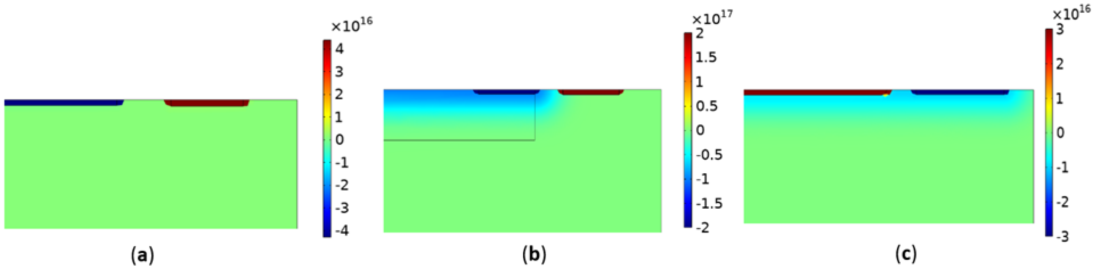
Figure 7 represents the spatial distribution of the differences between the concentrations of n-type and p-type dopants (represented by the semi.Na − semi.Nd (1/cm3) variable in COMSOL Multiphysics) in a zoomed region on the top of the cross-sections of the n+/p-substrate (a), n-well/p-substrate (b) and p+/n-well (c) photodiodes. In these figures, the orange or red zones have a positive value of the semi.Na − semi.Nd difference, which means that they contain a higher concentration of p-type dopants (acceptors). The blue zones correspond to a higher concentration of n-dopants (donors), and because of that, the semi.Na − semi.Nd has a negative value. Such dopant distributions are in agreement with the expected behavior of each p–n junction.
For all technologies, identical distributions to those shown in Figure 7 were obtained, varying only in the depth junctions and concentration of dopants. From these simulations, the results that characterize each photodiode for each of the technologies under study were obtained.
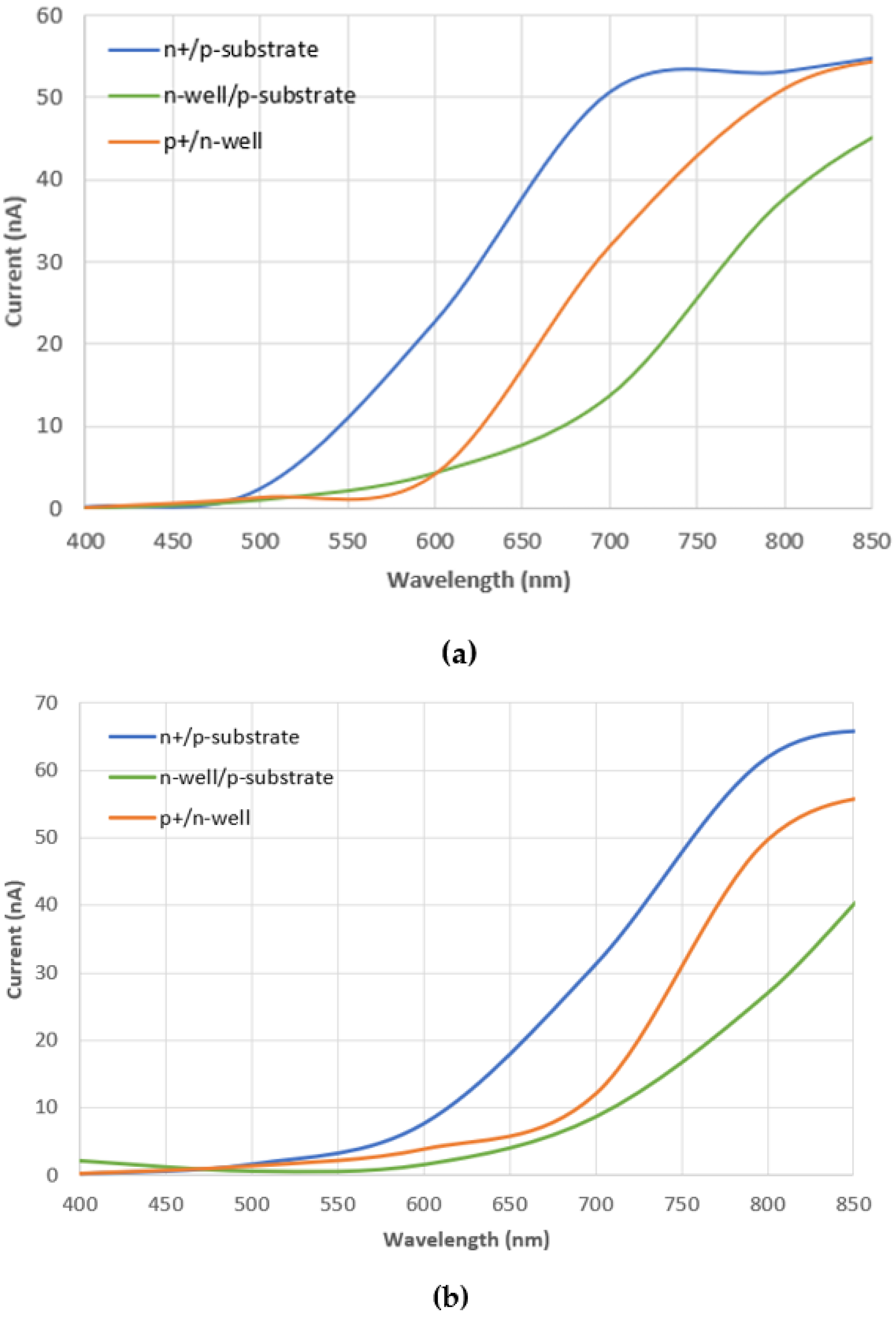
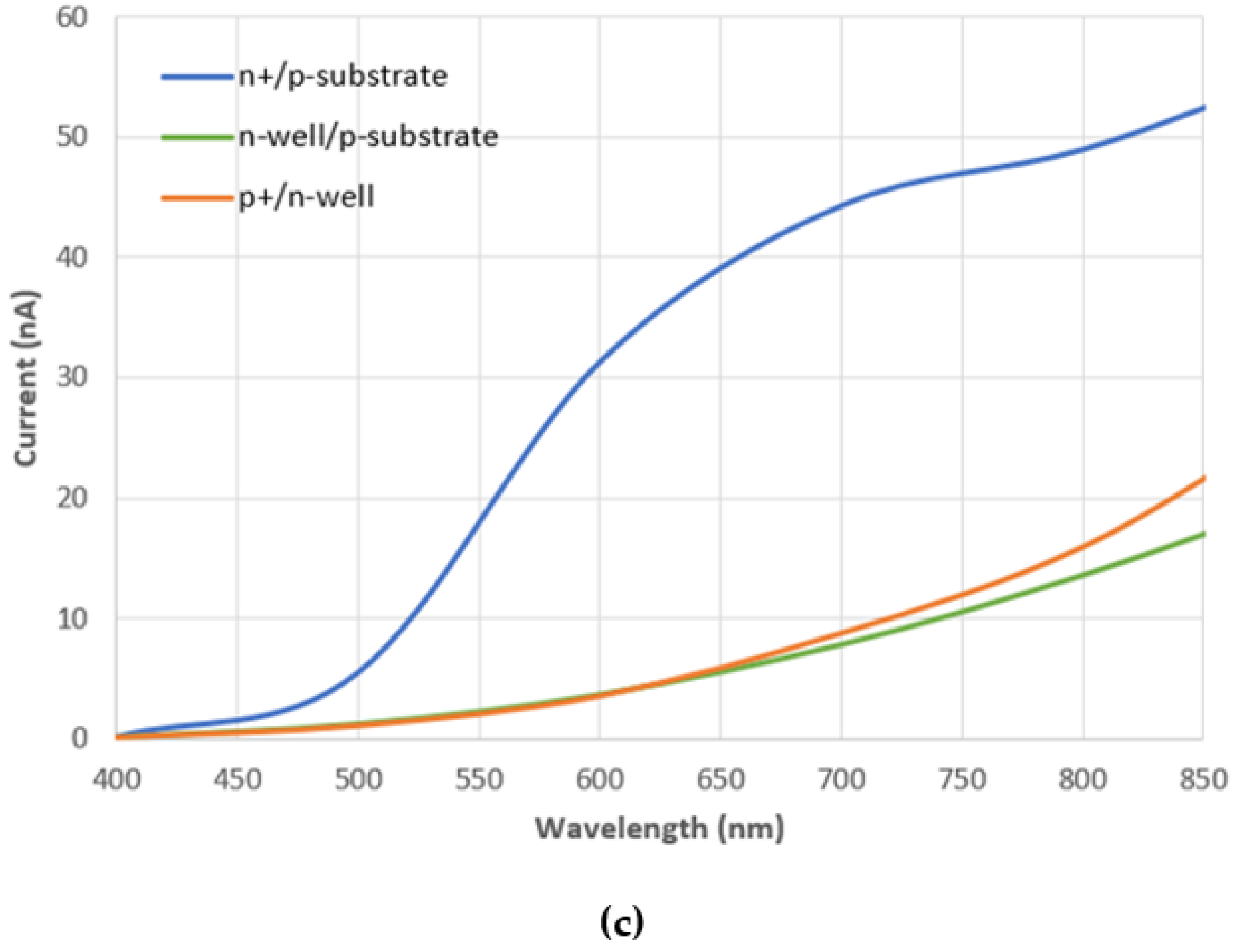
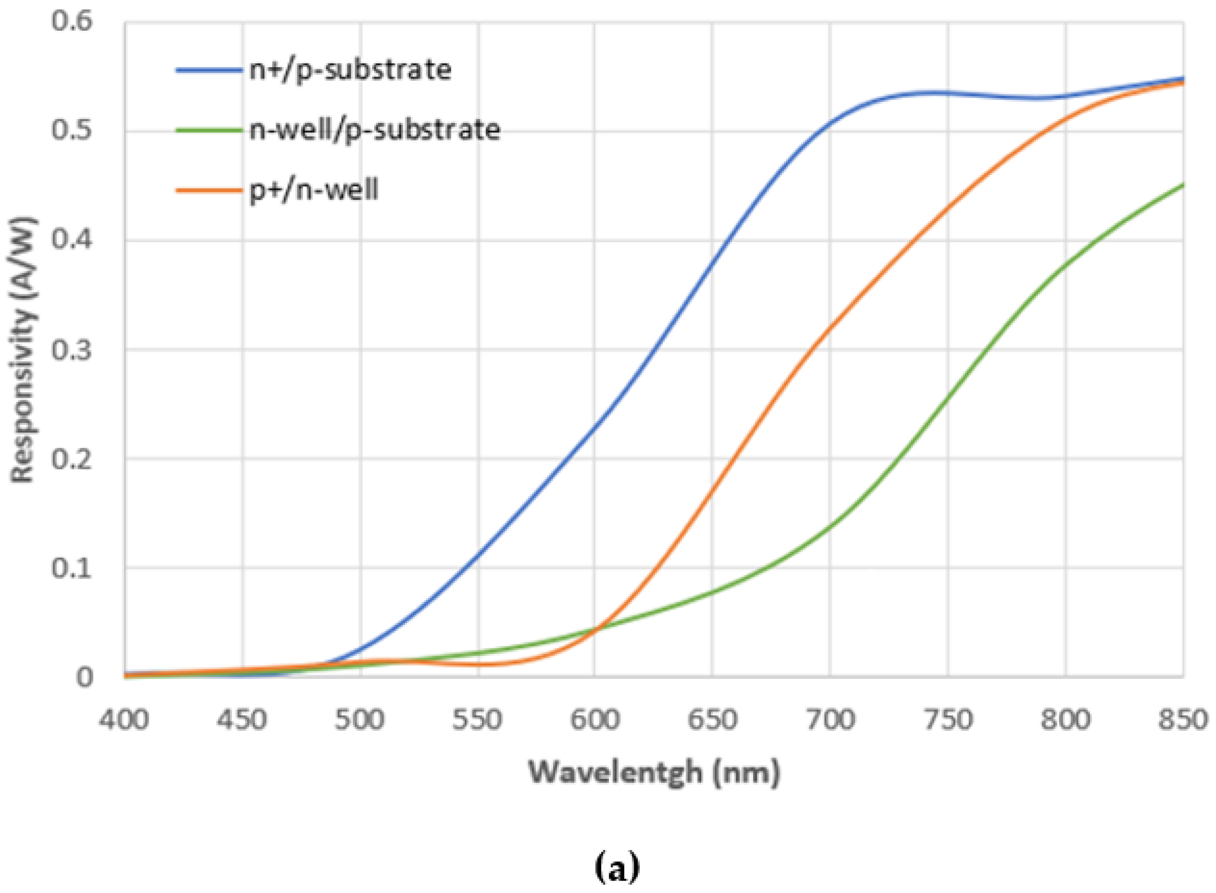
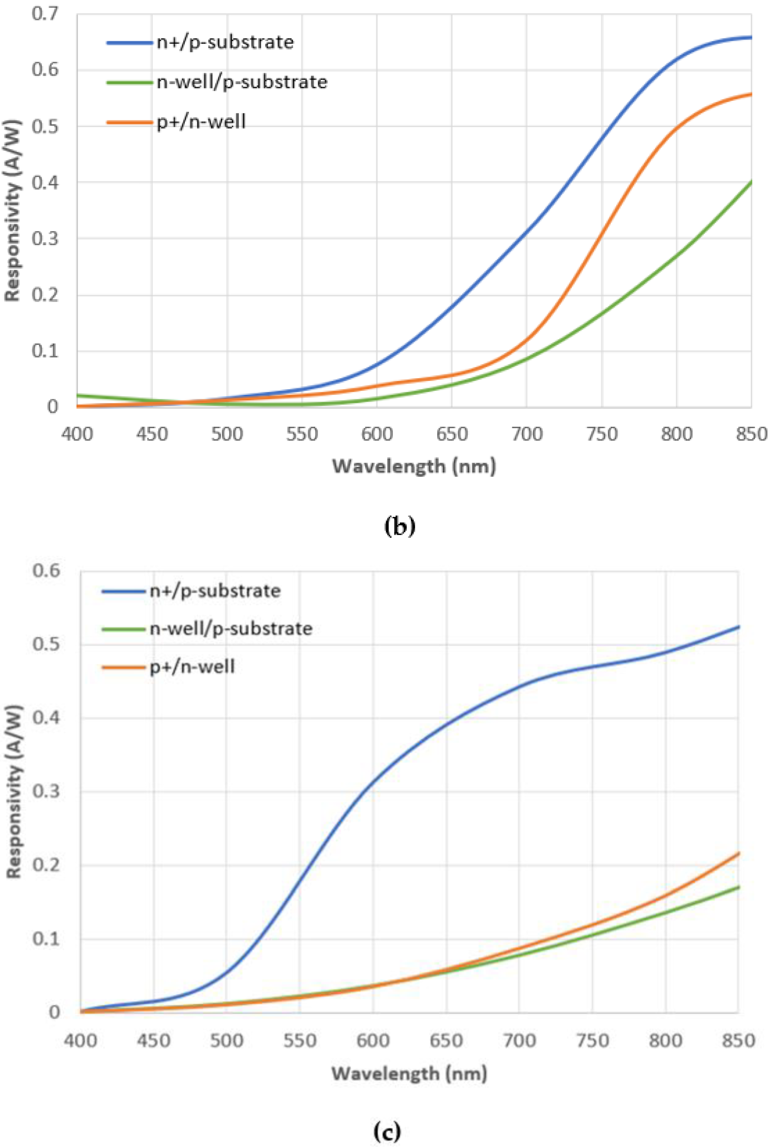
 Figure 8, Figure 9 and Figure 10 presents the numerical results of the current, responsivity and quantum efficiency plots, in the 400 nm–850 nm spectral range (obtained by a parametric sweep of the light wavelength), for the n+/p-substrate, n-well/p-substrate and p+/n-well photodiodes using the 0.18, 0.35 and 0.7 µm, respectively, in which the junctions’ depths and the concentrations of dopants were set according to Table 1 and Table 2, respectively. The spectral range 400 nm–850 nm was simulated, as it has been considered as the optical range needed for the optical detection system (as was the case in the development of a malaria diagnosis) [22].
Regarding the obtained results, the photodiode with the n+/p-substrate junction has a greater quantum efficiency across the spectrum for all simulated technologies. The n+/p-substrate photodiodes of the 0.18 µm and 0.35 µm technologies have a similar behavior and, thus, the choice also depends on the spectral range required for the target application. As the optical spectrum approaches the infrared region, the performances of the 0.35 µm and 0.18 µm photodiodes are very close, just slightly better for the 0.35 µm technology photodiode. However, according to the simulations for the visible spectral range, the 0.18 µm technology is the best option when a high quantum efficiency is required. Nonetheless, the 0.7 um technology also presents a curve with high quantum efficiency over the visible range, showing even higher quantum efficiency between 500–650 nm. The 0.7 µm technology has the lowest peak quantum responsiveness and efficiency within the visible range for all structures. Comparing all the curves for each technology, the results obtained are in agreement with the literature [7,23], since the n+/p-substrate photodiode seems to be the one with the highest quantum efficiency in the entire visible range of the optical spectrum. The n-well/p-substrate and p+/n-well photodiodes present, through the simulation, lower quantum efficiency values in the visible range of the spectrum. The n-well/p-substrate photodiode is the one with the lowest quantum efficiency over the entire spectrum. Despite the relatively good agreement with the literature showing the overall increase of the quantum efficiency with the increase of the wavelength, which is expected for silicon photodetectors, the numerical model of the p+/n-well photodiode fails to show, through the simulations, the expected decay in the 500–600 nm range, as predicted in Figure 2 and in the literature [1].
Overall, the simulations showed that the 0.18 µm technology presents a good performance characteristic within the visible optical range. Additionally, as previously stated, this technology is also the most suitable for integrating multisensing detection in the same chip (particularly high frequency acoustic sensors).
In addition to the optical characterization plots, the dark current (at 300 K) was also obtained for each photodiode structure, as shown in Table 5. According to the results, the dark current of a photodetector is the result of balanced contributions from the channel length (related to the junction depth) and from the dopants’ concentration. In particular, the dark current of a photodiode results from the contributions of the current due to carrier diffusion from the quasi-neutral regions, and the current due to generation in the space charge region. The major contributor for the dark current is the current due to generation in the space charge region, whose current density (jdc) can be given by the approximation (14) [24,25].
j d c = q · n i 2 ( x n τ 0 n + x p τ 0 p )
where q is the electron charge, ni is the intrinsic carrier concentration, τ 0 n and τ 0 p are the excess carriers’ lifetime, and xn and xp are the n-side and p-side depletion widths, respectively. The width of the depletion region (xn + xp) is inversely proportional to the space between the space charge region and the ohmic contact, and a wider junction depth leads to a wider space between this space charge region and the ohmic contact [25]. Thus, the larger the junction depth, the larger the space between the space charge region and ohmic contact, and the smaller the width of the depletion region, theoretically leading to a smaller current produced by the p–n junction in the absence of illumination, i.e., the dark current (accordingly to (13)). However, according to the results presented in Table 5 (and as previously mentioned), it can be observed that the dark current values depend not only on the channel length but also on the dopants’ concentration (acceptor and donor concentration (N0)). Their concentration is inversely proportional to the excess carrier lifetime ( τ 0 n and τ 0 p ) and, consequently, for higher concentration of dopants, the lifetime of excess carriers is shorter, leading to higher dark currents [24,25]. The dopant concentrations (acceptors and donors) vary significantly between the technologies. Thus, the results show that the dopant concentration also has a significant effect in the dark current photodiode response, alongside the junction depth. Additionally, the n+/p-substrate and p+/n-well photodiodes are the photodetectors with the highest dark current for all technologies. Nevertheless, all the simulated photodiodes show low dark currents (femtoamperes) in the numerical results, so it is expected that this interference can be neglected in experimental tests.
Table 6 presents, for comparison purposes, the performance of the photodiodes designed in the current study and other works reported in literature.
There are few studied reported in the literature on focused technologies (0.18, 0.35 and 0.7 µm) nor on specifying the photodetector p–n junction structures. Additionally, the results vary substantially among the studies, which further makes the comparison difficult. Overall, the quantum efficiency of a photodiode depends on the type of semiconductor (including the absorption coefficient), the depth of the junction, the width of the depletion layer, the distance between the charge space region and the ohmic contact, the dielectric coatings existing on the material surface, which affect the optical reflectance and the active area of the photodiode [30]. All these factors may cause the differences between the numerical simulations and the experimental characterizations reported in literature. First, it is important to note that the numerical results presented in Figure 8, Figure 9 and Figure 10 only took into account the p–n junction, without oxide layers on top of the photodiode’s active area, while the data reported in the literature (for instance [1]) includes oxides (with a different number of layers according to the technology), which affect the overall reflectance of the microstructure, also affecting its optical efficiency (when no anti-reflection coatings are considered) [31].
When comparing the simulation results with the experimental results reported in literature, it can be observed that, according to Table 6, the simulation of the n+/p-substrate photodiode in the 0.18 µm technology has the maximum peak of quantum efficiency in the same region (visible, between 500–700 nm) as the other n+/p-substrate photodiodes reported in the literature. The photodiode designed by Gabler et al. [29], although not specifying the p–n junction, has a similar behavior. This is the same for the photodiode presented by H. Tian et al. [28], which shows a lower quantum efficiency, but it is at 500 nm.
The simulation of the n+/p-substrate photodiode in the 0.35 µm technology reported in this work presents a quantum efficiency maximum of 97%, which similarly corresponds to the same maximum reached by Lee and Hornsey [26]. However, the efficiency peaks were reached in different regions, as the current work reports the peak near the infrared range (800 nm) and Lee and Hornsey in the visible range (650 nm). The simulation of the n-well/p-substrate 0.35 µm photodiode presents similar values of quantum efficiency maximum but occurs in different regions as those reported in the literature.
The n+/p-substrate 0.7 µm photodiode is characterized by a lower quantum efficiency, with a maximum value of 80%, different from the maximum values reported in the literature, but in the same regions of the optical spectrum. The n+/p-substrate photodiode simulated in the 0.7 µm technology also presents a significant difference in the quantum efficiency peak value in relation to the n+/p-substrate photodiode reported by Correia et al. [1], being significantly higher in the simulation (80% vs. 48%). Once again, this difference is explained by the presence, in the photodiode experimentally characterized and reported by Correia et al. [1], of the oxide layers over the photodiode active area, which have characteristic reflectance spectra, while it is only included the p–n junction in the simulations. These oxide layers contribute to the increase of the reflectance of the photodiode surface, decreasing its quantum efficiency. Such effect could be removed experimentally by adding anti-reflection coatings. The simulated n+/p-substrate 0.7 µm photodiode was also compared with similar junction photodiodes reported in the literature by Pimenta et al. [32], as presented in 
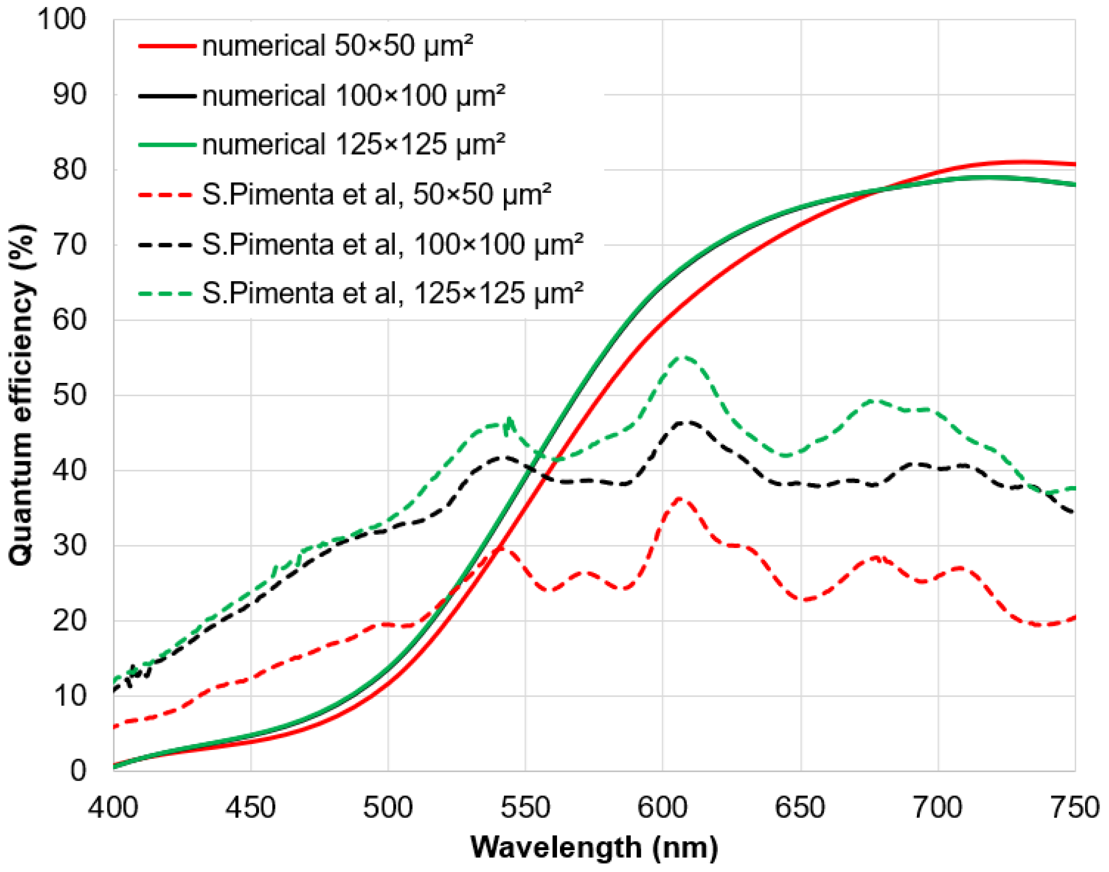
Figure 11. While the model reproduces the optical response of silicon, with an increase in the responsivity and quantum efficiency as the wavelength increases, a discrepancy between the results can be observed. Once again, it is due to the presence of oxide layers on top of the photosensitive areas of the experimentally characterized photodiodes, which led to the presence of small oscillations and peaks in the quantum efficiency spectra. Moreover, the experimental values suggested that larger active areas were related to photodiodes with higher quantum efficiency. However, such results may have occurred due to experimental difficulties in accurately measuring such small optical apertures. The simulated results show that, as expected, while there are small differences between the simulated curves, the active area has no significant importance in the quantum efficiency of a photodiode.
Finally, the simulation of the p+/n-well 0.7 µm photodiode reported in this work presents a similar quantum efficiency maximum in comparation to the literature. However, it occurs in a different region from the photodiode presented by Correia et al. With respect to n-well/p-substrate and p+/n-well photodiodes, since no other n-well/p-substrate and p+/n-well photodiodes have been reported in the literature for the 0.18 µm technology, these results cannot be directly compared.
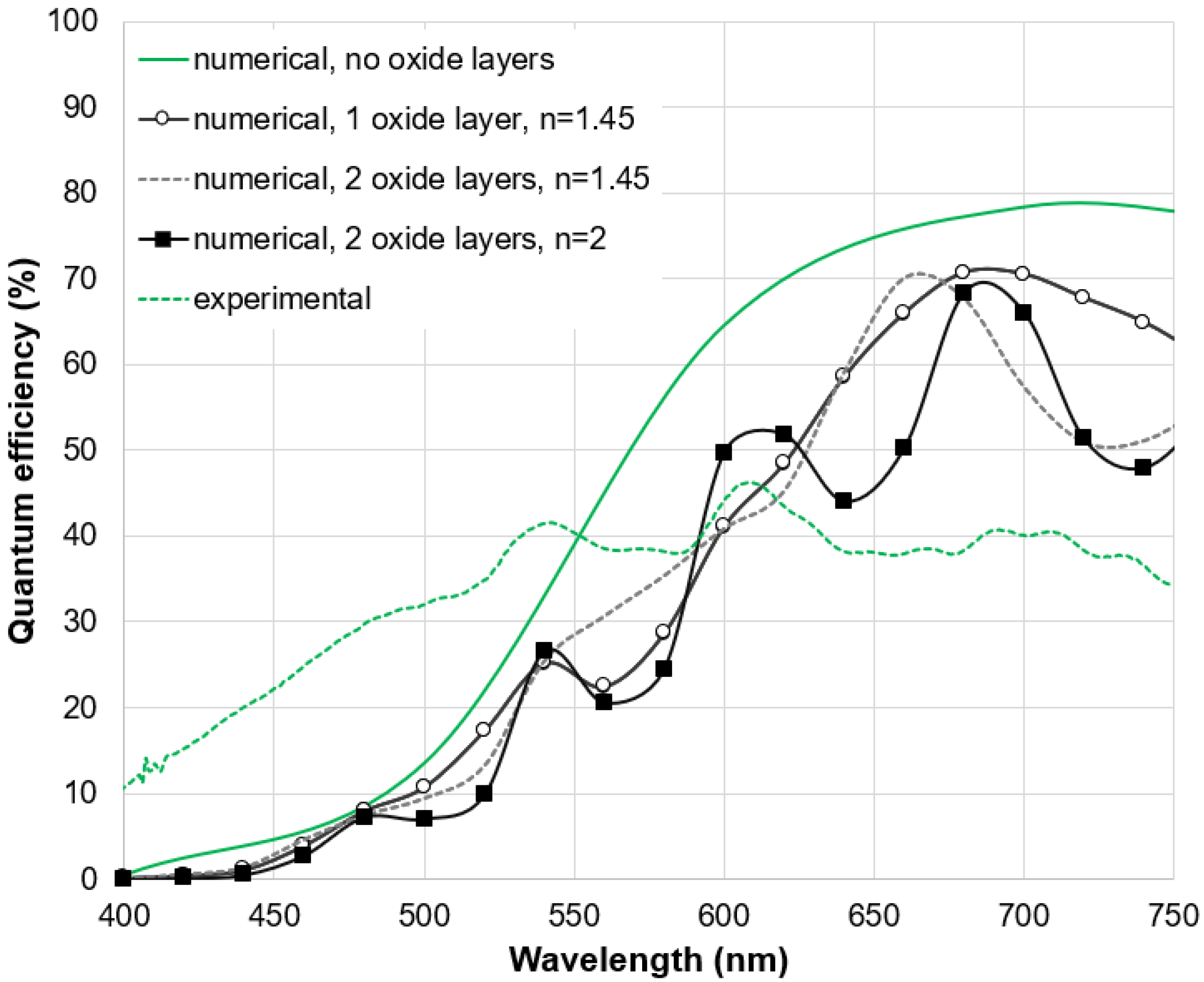
In order to evaluate the effect of different oxide layers on the optical behavior of photodiodes, Figure 12 presents the comparison between the quantum efficiency curves of a 100 × 100 µm2 n+/p-substrate photodiode, using the 0.7 µm technology, with and without oxide layers. For that purpose, the transmittance spectra of different oxide layers was evaluated, which was taken into account in the photodiode performance. To understand its influence, different simulations were performed, varying the number of oxides and their refractive index. The oxide thicknesses used correspond to the default layer thicknesses in the 0.7 μm technology (660 nm and 600 nm for oxides 1 and 2, respectively), according to [1]. The refractive indexes in the simulations correspond to the refractive index of silicon dioxide (SiO2), n = 1.45 and silicon nitride (Si3N4), n ≈ 2, for comparison purposes. From the new data, it was possible to obtain the quantum efficiency curve of the n+/p-substrate photodiode in the 0.7 µm technology with the effect of the oxides, as shown in the Figure 12. Comparing the results, it is verified that the obtained quantum efficiency curves have oscillation peaks similar to the experimental data available. It shows that, in fact, the presence of oxides and their characteristics (material, thickness and number of layers) affect the overall performance of the photodetector.
The results show that, globally, the greater the junction depth, the lower the expected quantum efficiency. This is explained by the fact that the depth of light penetration into silicon is wavelength dependent. Thus, shallow junctions (such as the n+/p-substrate or p+/n-well structures) collect the lower wavelengths of light more efficiently, while the higher efficiency presented by the n+/p-substrate, above 500 nm, is related to the difference in doping concentrations between the n and p sides, which extends the p-side depletion area deeper [12].
Finally, the dark current values have the same order of magnitude in the simulations and in the literature, which brings confidence to the results obtained.

4. Conclusions and Future Works

This paper describes the design, numerical simulation, and characterization of vertical CMOS photodiodes in silicon p–n junctions. Three CMOS photodiode structures were considered: n+/p-substrate, n-well/p-substrate and p+/n-well. Initially, the CMOS photodiode structures were characterized for the 0.18 µm, 0.35 µm and 0.7 µm CMOS technologies. The simulation results show that the photodiodes with 0.18 and 0.35 µm technologies are those with the highest peak quantum efficiency in the visible range (400–800 nm). Similarly, the photodiode in the 0.7 µm technology proved to be the one with the lowest peak quantum efficiency, showing that, from the simulations, the greater the depth of the junctions, the lower the quantum efficiency in the visible range. Additionally, when comparing the different photodiodes’ junction structures, the n+/p-substrate photodiode presented the best quantum efficiency curve in the visible range, which is in agreement with the literature. Regarding the dark current values and comparing with the literature, the results are in similar magnitude orders (pA and fA), but the variation of dark currents between technologies and p–n junctions is not entirely clear, being dependent both on the junctions’ depth and on the dopant concentrations.
Additionally, regarding the effect of oxide interference in the performance of the photodetectors, it was found that they significantly influence the quantum efficiency curves (both the number of layers, thickness and refractive index of the materials). Furthermore, the foundries where the photodiodes are manufactured also lead to slight variations in the fabrication parameters and, consequently, different performance of the photodiodes.
These results demonstrate that, even with technologies that allow high integration, it is possible to obtain photodiodes with good performance features. Furthermore, the results obtained demonstrate that COMSOL is a tool that enables the numerical characterization of silicon photodiodes in CMOS with relative confidence. However, COMSOL still has some relevant limitations in the integration of optics and semiconductor physics, in particular when describing the expected decay in the quantum efficiency curves of p+/n-well photodiodes, in the 500–600 nm range.
Nevertheless, based on the achieved results, the authors designed the layout of n+/p-substrate, n-well/p-substrate and p+/n-well photodiodes, aiming the fabrication and integration of such photodetectors into a multiphysics sensing CMOS chip based on 0.18 µm technology. Integration into a detection and readout system for malaria diagnosis will be the next step of the development work [22].

Author Contributions

Conceptualization, G.M.F., G.M. and S.O.C.; methodology, G.M.F., V.S., G.M. and S.O.C.; validation and analysis, G.M.F., V.S. and S.O.C.; investigation, G.M.F. and V.S.; resources, G.M. and S.O.C.; writing—original draft preparation, G.M.F.; writing—review and editing, G.M. and S.O.C.; supervision, G.M. and S.O.C.; project administration, S.O.C.; funding acquisition, S.O.C. All authors have read and agreed to the published version of the manuscript.

Funding

This work was supported by Project NORTE-01-0145-FEDER-028178 funded by NORTE 2020 Portugal Regional Operational Program under PORTUGAL 2020 Partnership Agreement through the European Regional Development Fund and the Fundação para a Ciência e Tecnologia (FCT), IP. This work was also supported by national funds, through the Portuguese FCT, under the reference projects UIDB/04436/2020 and UIDP/04436/2020. V. Silva thanks FCT for the grant SFRH/BD/137529/2018 funded by COMPETE 2020. Susana Catarino thanks FCT for her contract funding provided through 2020.00215.CEECIND.

Institutional Review Board Statement

Not applicable.

Informed Consent Statement

Not applicable.

Data Availability Statement

All data are available upon request to the corresponding author.

Conflicts of Interest

The authors declare no conflict of interest. The funders had no role in the design of the study; in the collection, analyses, or interpretation of data; in the writing of the manuscript, or in the decision to publish the results.

References

  1. Correia, R.G.; Pimenta, S.; Minas, G. CMOS Integrated Photodetectors and Light-to-Frequency Converters for Spectrophotometric Measurements. IEEE Sens. J. 2017, 17, 3438–3445. [Google Scholar] [CrossRef]
  2. Kuo, W.-C.; Chiang, C.-T.; Huang, Y.-C. An Automatic Light Monitoring System with Light-to-Frequency Converter for Flower Planting. In Proceedings of the 2008 IEEE Instrumentation and Measurement Technology Conference, Victoria, BC, Canada, 12–15 May 2008; pp. 1146–1149. [Google Scholar] [CrossRef]
  3. Betta, G.-F.D. (Ed.) Advances in Photodiodes; InTechOpen: London, UK, 2011. [Google Scholar]
  4. Bigas, M.; Cabruja, E.; Forest, J.; Salvi, J. Review of CMOS image sensors. Microelectron. J. 2006, 37, 433–451. [Google Scholar] [CrossRef] [Green Version]
  5. Campbell, S.A. The Science and Engineering of Microelectronic Fabrication, 2nd ed.; Oxford University Press: Oxford, UK, 2001. [Google Scholar]
  6. Titus, A.H.; Cheung, M.C.; Chodavarapu, V.P. CMOS Photodetectors; IntechOpen: London, UK, 2011. [Google Scholar] [CrossRef] [Green Version]
  7. Moini, A. Vision Chips; Springer: Boston, MA, USA, 2000. [Google Scholar]
  8. Hirayama, T. The evolution of CMOS image sensors. In Proceedings of the 2013 IEEE Asian Solid-State Circuits Conference (A-SSCC), Singapore, 11–13 November 2013; pp. 5–8. [Google Scholar]
  9. Konstantinidis, A.C.; Szafraniec, M.B.; Rigon, L.; Tromba, G.; Dreossi, D.; Sodini, N.; Liaparinos, P.F.; Naday, S.; Gunn, S.; McArthur, A.; et al. X-ray Performance Evaluation of the Dexela CMOS APS X-ray Detector Using Monochromatic Synchrotron Radiation in the Mammographic Energy Range. IEEE Trans. Nucl. Sci. 2013, 60, 3969–3980. [Google Scholar] [CrossRef] [Green Version]
  10. Leblebici, Y.; Kang, S.-M. CMOS Digital Integrated Circuits Analysis and Design, 3rd ed.; McGraw-Hill: New York, NY, USA, 2003. [Google Scholar]
  11. Chuah, J.H.; Holburn, D. An integrated solid-state solution for secondary electron detection. Analog. Integr. Circuits Signal Process. 2013, 79, 395–411. [Google Scholar] [CrossRef]
  12. Fernandes, A.V.; Cardoso, V.F.; Rocha, J.G.; Cabral, J.; Minas, G. Smart-Optical Detector CMOS Array for Biochemical Parameters Analysis in Physiological Fluids. IEEE Trans. Ind. Electron. 2008, 55, 3192–3200. [Google Scholar] [CrossRef]
  13. De Baena, M.S.; Minas, G.; Catarino, S. PVDF piezoelectric flow sensor for velocity measurements aiming malaria diagnostics: A preliminary approach. In Proceedings of the 2019 IEEE 6th Portuguese Meeting on Bioengineering (ENBENG), Lisbon, Portugal, 22–23 February 2019; pp. 1–4. [Google Scholar]
  14. COMSOL Multiphysics. Semiconductor Module User’s Guide. COMSOL 5.3. 2017. Available online: https://doc.comsol.com/5.3/doc/com.comsol.help.semicond/SemiconductorModuleUsersGuide.pdf (accessed on 1 October 2021).
  15. Alirezaei, I.S.; Burte, E.P. Modeling and simulation of a 3D-CMOS silicon photodetector for low-intensity light detection. Phys. Simul. Optoelectron. Devices XXIV 2016, 9742, 974208. [Google Scholar] [CrossRef]
  16. Green, M.A.; Keevers, M.J. Optical Properties of Intrinsic Silicon at 300 K. Prog. Photovolt. Res. Appl. 1995, 3, 189–192. [Google Scholar] [CrossRef]
  17. United Microelectronics Corportation (UMC). 1P6M Metal Metal Capacitor Process Topological Electrical Design Rule. Version 2.11_P. 1. UMC: Hsin-Chu City, Taiwan, 2008. Available online: https://www.umc.com/en/StaticPage/design_support_manual (accessed on 1 July 2021).
  18. Austria Micro Systems (AMS) 0.35 µm CMOS C35 Process Parameters, Eng-182 Rev.2.0; AMS: Schloss Premstätten, Austria, 2003.
  19. Minas, G.; Ribeiro, J.; Wolffenbuttel, R.; Correia, J. On-chip integrated CMOS optical detection microsystem for spectrophotometric analyses in biological microfluidic systems. In Proceedings of the EEE International Symposium on Industrial Electronics, Dubrovnik, Croatia, 20–23 June 2005; Volume 3, pp. 1133–1138. [Google Scholar]
  20. Kamrani, E. On-Chip Integrated Functional Near Infra-Red Spectroscopy (fNIRS) Photoreceiver for Portable Brain Imaging (PhD thesis, École Polytechnique de Montréal). Available online: https://publications.polymtl.ca/1346 (accessed on 3 January 2022).
  21. Sanabria, C.; Aranda, M.L. Electromagnetic analysis of via arrays for different RF-CMOS technological nodes. In Proceedings of the 2019 16th International Conference on Electrical Engineering, Computing Science and Automatic Control (CCE), Mexico City, Mexico, 11–13 September 2019; pp. 1–6. [Google Scholar] [CrossRef]
  22. Costa, M.; Baptista, V.; Ferreira, G.; Lima, D.; Minas, G.; Veiga, M.; Catarino, S. Multilayer Thin-Film Optical Filters for Reflectance-Based Malaria Diagnostics. Micromachines 2021, 12, 890. [Google Scholar] [CrossRef] [PubMed]
  23. Minas, G.; Martins, J.; Ribeiro, J.; Wolffenbuttel, R.; Correia, J. Biological microsystem for measuring uric acid in biological fluids. Sens. Actuators A Phys. 2004, 110, 33–38. [Google Scholar] [CrossRef] [Green Version]
  24. Information Systems Laboratory. Lecture EE 392B: Silicon Photodetectors; Stanford University: Stanford, CA, USA; pp. 1–75. Available online: https://isl.stanford.edu/~abbas/ee392b/lect01.pdf (accessed on 3 January 2022).
  25. Muller, R.S.; Kamins, T.I. Device Electronics for Integrated Circuits, 3rd ed.; John Wiley & Sons: Hoboken, NJ, USA, 2003. [Google Scholar]
  26. Lee, J.S.; Hornsey, R.I. Improved One-dimensional Analysis of CMOS Photodiode Including Epitaxial-Substrate Junction. In Proceedings of the 2001 IEEE Workshop on CCDs and Advanced Image Sensors, Lake Tahoe, NV, USA, 7–9 June 2001; pp. 106–109. Available online: http://www.cse.yorku.ca/~visor/pdf/1D_PD_CCD&AIS%2701.pdf (accessed on 3 January 2022).
  27. Fernandes, A.; Rocha, J.G.; Minas, G. Smart-Pixel Array for Imaging Sensors. In Proceedings of the 2007 14th IEEE International Conference on Electronics, Circuits and Systems, Marrakech, Morocco, 11–14 December 2007; pp. 395–398. [Google Scholar] [CrossRef] [Green Version]
  28. Tian, H.; Liu, X.; Lim, S.; Kleinfelder, S.; El Gamal, A. Active pixel sensors fabricated in a standard 0.18-μm CMOS technology. SPIE Proc. 2001, 4306, 441–449. [Google Scholar] [CrossRef]
  29. Gäbler, D.; Henkel, C.; Thiele, S. CMOS Integrated UV-Photodiodes. Procedia Eng. 2016, 168, 1208–1213. [Google Scholar] [CrossRef]
  30. Sze, S.M. Physics of Semiconductors Devices, 2nd ed.; John Wiley & Sons: New York, NY, USA, 1981. [Google Scholar]
  31. Mohamad, W.; Hajar, A.A.; Saleh, A. Effects of oxide layers and metals on photoelectric and optical properties of Schottky barrier photodetector. Renew. Energy 2006, 31, 1493–1503. [Google Scholar] [CrossRef]
  32. Pimenta, S.; Carmo, J.P.; Correia, R.G.; Minas, G.; Castanheira, E.M.S. Characterization of silicon photodiodes for diffuse reflectance signal extraction. In Proceedings of the 2015 IEEE 4th Portuguese Meeting on Bioengineering (ENBENG), Porto, Portugal, 26–28 February 2015; pp. 1–4. [Google Scholar] [CrossRef] [Green Version]
Figure 1. Cross-section views (non-scaled) of the standard photodiodes’ designs in CMOS technology: (a) n-well/p-substrate, (b) p+/n-well and (c) n+/p-substrate. The orange shading on top represents the active area of each photodiode, i.e., the photosensitive region.
Applsci 12 02580 g001
Figure 2. Estimation of the quantum efficiency curves for the 3 types of vertical silicon photodiodes manufactured in CMOS technology (2 µm): p+/n-well, n+/p-substrate and n-well/p-substrate (data estimated from [7]).
Applsci 12 02580 g002
Figure 3. Illustrative example of a n+/p-substrate photodiode simulation: (a) complete geometry and (b) detail of the top of the photodiode. The dark blue area represents the p+ doping on the p-type silicon substrate. In the center, the colored area represents the n+ doping region, representing the active area of the photodiode, with a 100 µm width (represented by the dimension a). d0 represents the substrate thickness; the value of 500 µm was used. The length of the p + doping zones (represented in the figure by the dimension b) considered was 2 µm for all technologies. Photodiodes manufactured using the 0.18 µm technology have this same value. The total width of the photodiode is 110 µm.
Applsci 12 02580 g003
Figure 4. (a) View of the 2D mesh applied to the n+/p-substrate photodiode in 0.18 μm technology and (b) zoomed view of the blue square in the left figure where it is possible to observe the meshing of the n+ and p+ doping regions with higher detail.
Applsci 12 02580 g004
Figure 5. Top: Layout of the 3 types of photodiodes in 0.18 µm CMOS technology: (a) n+/p-substrate, (b) n-well/p-substrate and (c) p+/n-well. Bottom: Zoom of the lower right corner of each photodiode layout, allowing the visualization of the contacts (green dots): (a.1) n+/p-substrate, (b.1) n-well/p-substrate and (c.1) p+/n-well.
Applsci 12 02580 g005
Figure 6. Layout of the photodiodes’ area in the chip, ready to be sent to the silicon foundry, with the designed photodiodes included: A—n+/p-substrate, A’—n+/p-substrate covered with metal, B—n-well/p-substrate, B’—n-well/p-substrate covered with metal, C—p+/n-well, C’—p+/n-well covered with metal and D—pad for external connection. The total dimension of the photodetector chip is 0.7 mm × 1.1 mm.
Applsci 12 02580 g006
Figure 7. Spatial distribution of the differences between the concentrations of n-type and p-type dopants (represented by the color range of the semi.Na − semi.Nd (1/cm3) variable, in COMSOL Multiphysics), at the 800 nm wavelength, in a zoomed region (around 10 μm depth) on the top of the cross-sections of the n+/p-substrate (a), n-well/p-substrate (b) and p+/n-well (c) photodiodes in 0.18 µm technology.
Applsci 12 02580 g007
Figure 8. Current (nA) of n+/p-substrate, n-well/p-substrate and p+/n-well photodiodes in (a) 0.18 µm, (b) 0.35 µm and (c) 0.7 µm technologies in COMSOL.
Applsci 12 02580 g008aApplsci 12 02580 g008b
Figure 9. Responsivity (A/W) of n+/p-substrate, n-well/p-substrate and p+/n-well photodiodes in (a) 0.18 µm, (b) 0.35 µm and (c) 0.7 µm technologies in COMSOL.
Applsci 12 02580 g009aApplsci 12 02580 g009b
Figure 10. Quantum efficiency (%) of n+/p-substrate, n-well/p-substrate and p+/n-well photodiodes in (a) 0.18 µm, (b) 0.35 µm and (c) 0.7 µm technologies in COMSOL.
Applsci 12 02580 g010
Figure 11. Comparison between the numerical (simulated in COMSOL) and experimental (data obtained from [32]) quantum efficiency (%) of n+/p-substrate photodiodes using the 0.7 µm technology.
Applsci 12 02580 g011
Figure 12. Comparison between the numerical (simulated in COMSOL) and experimental (data obtained from [32], when it was considered 2 oxide layers) quantum efficiency (%) of n+/p-substrate photodiodes with 100 × 100 µm2 using the 0.7 µm technology, with and without oxide layers on top of the photodiodes. In the plots, n corresponds to the refractive index of the oxide layers.
Applsci 12 02580 g012
Table 1. Junction depths for CMOS technologies 0.18 µm, 0.35 µm and 0.7 µm [17,18,19].
CMOS TechnologyJunction Depth n+ (dn) (µm)Junction Depth p+ (dp) (µm)n-Well Depth (dnw) (µm)
0.18 µm0.160.181.8
0.35 µm0.200.202.0
0.7 µm0.350.352.5
Table 2. Acceptor and donor concentrations (1/cm3) for technologies 0.18 µm, 0.35 µm and 0.7 µm [20].
CMOS TechnologyAcceptor Concentration in p-Substrate (Nb) (1/cm3)Donor Concentration n+ (N0) (1/cm3)Acceptor Concentration p+ (N0) (1/cm3)Donor Concentration n-Well (N0) (1/cm3)
0.18 µm1.14 × 10154.38 × 10194.30 × 10191.19 × 1017
0.35 µm1.25 × 10155.00 × 10195.00 × 10191.28 × 1017
0.7 µm *1.42 × 10156.80 × 10196.80 × 10191.35 × 1017
* Values were calculated through a linear regression, since they were not found in literature.
Table 3. Additional relevant parameters included in the numerical simulations.
Hole lifetime10 µs
Electron lifetime10 µs
Incident optical power0.1 µW
Substrate thickness (d0)500 µm
Table 4. Number of mesh elements and quality statistics of the mesh.
CMOS TechnologyCMOS StructureNumber of ElementsMinimum Quality (a.u.)Average Quality (a.u.)
0.18 µmn+/p-substrate25,7840.55960.9027
n-well/p-substrate36,0360.56160.9153
p+/n-well26,5770.46610.9133
0.35 µmn+/p-substrate23,4040.56990.9106
n-well/p-substrate35,9200.44220.9145
p+/n-well22,9670.39090.9147
0.7 µmn+/p-substrate29,9690.55240.9039
n-well/p-substrate16,7690.53950.9335
p+/n-well20,4980.48680.9188
Table 5. Dark current (fA) measured at 300 K of the n+/p-substrate, p+/n-well and n-well/p-substrate photodiodes simulated for 0.18, 0.35 and 0.7 µm CMOS technologies.
CMOS Technologyn+/p-Substrate (fA)p+/n-Well (fA)n-Well/p-Substrate (fA)
0.18 µm370119331653
0.35 µm18402179675
0.7 µm41642205802
Table 6. Quantum efficiency and dark current values for different technologies and photodiodes’ structures in the literature.
AuthorsCMOS TechnologyPhotodiode StructureMaximum Quantum EfficiencyActive AreaDark CurrentRef.
J. Chuah and D. Holburn0.35 µmn-well/p-substrate63% (550 nm)100 × 100 µm24.5 fA[11]
J. S. Lee and R. I. Hornsey0.35 µmn+/p-substrate85% (650 nm)non definednon defined[26]
R. G. Correia et al.0.7 µmn+/p-substrate≈48% (620 nm)100 × 100 µm2144 fA[1]
R. G. Correia et al.0.7 µmp+/n-well≈40% (480 nm)100 × 100 µm24.390 pA[1]
A. Fernandes et al.0.7 µmn+/p-substratenon defined100 × 100 µm29.6 fA[27]
H. Tian et al.0.18 µmn+/p-substrate22% (500 nm)4 × 4 µm22.4 fA[28]
D.Gabler et al.0.18 µmTypical photodiode (junction non specified)≈73% (700 nm)non definednon defined[29]
This work n+/p-substrate90% (700 nm)100 × 100 µm23701 fA
0.18 µmp+/n-well80% (800 nm)1933 fA
n-well/p-substrate65% (850 nm)1653
n+/p-substrate97% (820 nm)1840 fA
0.35 µmp+/n-well82% (820 nm)2179 fA
n-well/p-substrate60% (850 nm)675 fA
n+/p-substrate80% (720 nm)4164 fA
0.7 µmp+/n-well30% (850 nm)2205 fA
n-well/p-substrate25% (850 nm)802 fA
Publisher’s Note: MDPI stays neutral with regard to jurisdictional claims in published maps and institutional affiliations.

