
PCB Network Analysis for Circuit Partitioning


School of Automation Engineering, University of Electronic Science and Technology of China, Chengdu 611731, China
*
Authors to whom correspondence should be addressed.
Appl. Sci. 2022, 12(16), 8200; https://doi.org/10.3390/app12168200
Submission received: 25 July 2022
/
Revised: 11 August 2022
/
Accepted: 12 August 2022
/
Published: 17 August 2022
(This article belongs to the Special Issue Advances in Artificial Intelligence for Perception Augmentation and Reasoning)
Abstract
:The complexity of automatic placement and routing is proportional to the scale of the circuit. Through netlist partition algorithms, printed circuit board (PCB) circuits are divided into different submodules, and the problem scale is effectively reduced in order to obtain the optimal automatic layout and routing. In this paper, we analyze net attributes and potential patterns in netlists through visualization, and propose a heuristic PCB netlist partition approach based on net attributes and potential patterns which we discover from netlists. Our partition approach takes the netlist as input, and module partition set as output. Firstly, the modules are prepartitioned using net attributes. Further, the special patterns in circuits are discovered, and the scattered resistors, capacitors, and other components caused by prepartitioning would be allocated to initial modules by three rules—classifying, matching, and force strategy. Our method is evaluated on 11 PCB netlists which are built manually. Experimental results show that our proposed netlist partition approach significantly outperforms the state of the art on all evaluation indices, which can achieve 80–96% partition accuracy.
1. Introduction
Placement and routing, also known as physical design, typically account for more than 30% of cost and time in integrated circuit (IC) or PCB design and production. If automatic placement and routing can be implemented, it will effectively shorten the production cycle and reduce costs, and reduce the risk of human mistake. Thus, automatic placement and routing has been an interesting and challenging research direction in the field of electronic design automation (EDA). However, whether it is the placement and routing inside the chip or PCB level, the design process is very complicated. The design complexity of modern integrated circuits has greatly increased as circuits have become larger and contain more and more components. As we all know, the complexity of automatic placement and routing is proportional exponentially to the scale of the circuit [1], and it is a nondeterministic polynomial hard (NP-hard) problem. So far, it has not been practically applied, mainly relying on manual implementation. Physical design usually consists of six main steps: module partition, chip planning, placement, clock tree synthesis, routing, and timing closure [2]. The first step of circuit partition is to divide the problem into smaller submodules, which can effectively reduce the complexity of the problem, reduce the search space for automatic placement and routing, and obtain an optimal solution. If the module can be partitioned correctly, it also improves the parallelism of automatic placement and routing, so as to improve the efficiency, the stability, and quality of module placement and routing.
The netlist is the logical basis for physical design. A netlist contains components and pin connections between components, represented as nodes, and network connections between nodes. Components mainly include resistors, capacitors, inductors, magnetic beads, crystal oscillators, two-pin switches, diodes, and other two-pin components, as well as IC chips, connectors, transistors, multi-pin LEDs, multi-pin switches, and other multi-pin components. Connections exist not only between two components, but also between multiple components. The existing circuit partition methods mainly represent the netlist in a hypergraph. Assuming a hypergraph has node set with K nodes, and edge (net) set , partition methods aim to divide the K nodes into N subsets with set size , respectively.
Most of the existing hypergraph-based partitioning methods were proposed before 20 years ago [3,4]. Although a partition set can be obtained, the partition result is hard to effectively evaluate, and it is far from being applied in the practical application. With the development of electronic-aided design technology, the design process is more standardized, and potential patterns contained in the netlist are more regular. Inspired by the manual partitioning of physical modules, in this paper we focus on the potential features and attributes contained in the netlist, and propose a circuit module partitioning method based on the analysis of netlist network attributes and potential patterns. The partition algorithm takes the PCB netlist as input, and the module subsets as output. It is expected that these partition modules can not only be physically adjacent, but also functionally independent. The main contributions of this paper are as follows:
- (1)
- The visualization analysis, attribute analysis, and pattern analysis of netlists are carried out, and the potential features and attributes in netlists are discovered.
- (2)
- Based on the potential features and attributes, a new approach to PCB netlist partition is proposed. The method first prepartitions the PCB netlist according to the network attributes, then presents three rules of classifying, matching, and force to redistribute the scattered components, and finally obtains the partition subsets.
- (3)
- The partition approach is evaluated on 11 netlists, outperforming the state of the arts on five different metrics. Experiments show that our approach based on network attributes and potential patterns can obtain 80–96% accuracy.
A preliminary version of this work was published in [5]. This paper improves upon [5] in the following aspects: (1) the netlist visualization is studied to help netlist analysis, and inspires us to develop algorithms of partition; (2) some generic circuit patterns and repetitive patterns are analyzed, which is meaningful for netlist partition; (3) our algorithm is analyzed at each stage using different rules, and we report the evaluation indices to show the necessity of each stage.
This paper is divided into six parts. Section 2 is the related research work. Section 3 discusses the discovery of potential patterns and analysis of network attributes in the netlist. Section 4 describes the partition method based on network attribute and patterns, and a large number of experiments illustrate the effectiveness of the proposed method in Section 5. Section 6 gives a discussion on experiments. Section 7 concludes and gives some thoughts on the future work.
2. Related Work
As mentioned above, the netlist is usually represented as a graph—a point set and an edge set between points and points, and the edge set can be attached with weights to become a weighted graph [6]. The existing netlist partitioning algorithms mainly consider two types of problems:
- (1)
- How to divide, that is, the partition strategy;
- (2)
- How to reduce the time complexity of partition, that is, the partition efficiency [7].
Partition strategies can be roughly classified into four categories: methods based on graph cut by flow [8,9,10,11], heuristic methods [1,12], eigenvector method [13], and combinations of these methods [11,14,15,16]. Generally, the methods based on graph cut have high time complexity, and the heuristic algorithms are relatively fast. All these types of algorithms can be combined into a multilevel framework [3,11,17,18], which mainly divides the partition problem into multiple levels to reduce the scale of the problem, and leads to reduce the time complexity of partition.
Heuristic methods: Kernighan and Lin proposed a netlist partition algorithm, called KL algorithm, which is the most classic of the heuristic methods [1]. The KL algorithm partitions components by evaluating a heuristic value D, which is computed from the cost matrix, and it is a two-way partition approach applied to component partition on circuit boards. The KL algorithm was extended to different variations. Manna et al. [19] used the KL algorithm to partition on mesh-based network-on-chip. Rajan and Bhaiya [20] considered a parallel KL algorithm to partition the component on very-large-scale integrated circuit (VLSI) for fast solution. Manna and Teja [21] extended the KL algorithm to 3D network-on-chip, while Lei et al. extended the KL algorithm by using the balanced bi-partition theory of graphs, and improved it by giving a reasonable initial partition in the multilevel framework [22]. Areibi and Vannelli in [12] proposed a cluster-based heuristic method. They extracted component attributes from netlist, including component terminal count, common net count, the number of nets localized, common net fanout, and so on, to identify strongly connected components to reduce the netlist complexity.
Graph cut methods: Netlists are natural graphs with nodes and connection, so the traditional graph cut algorithms were easily taken to the netlist partition. Wei and Cheng presented a partition method called ratio cut, and solved the ratio cut by linear programming techniques via the MaxFlow [23], while Hamada et al. ultilized the ratio cut in the hierarchical way in [11]. Fiduccia and Matteyses [14] combined the min-cut and KL algorithm, and proposed an iterative min-cut heuristic method with a linear time, called FM algorithm. Liu et al. [9] proposed a two-way partition strategy by solving a replication graph cut problem. Karypis et al. [3] presented a multilevel paradigm of coarse-to-coarser to partition hypergraph in VLSI with over 100k vertices. Caldwell et al. [4] provided an implementation of hypergraph partition in VLSI. However, these methods only treated the netlist as a pure graph, so only the geometric connection of the netlist was considered in the partition process.
Eigenvector methods: Hadley et al. approximated the netlist as a weighted graph, and initially partitioned the weighted graph into k blocks of fixed module size by the eigenvector technique of Barnes [6]; they also gave the lower bounds on the number of cut nets using the tightly underestimated graph approximation and the simple eigenanalysis results [13].
Other methods: Monolithic 3D (M3D) integrated circuits are a promising technology that improves integration density greatly, which is orders of magnitude higher than that offered by through-silicon-vias, so the partition of M3D netlists has attracted a number of researchers [19,24,25,26]. Manna et al. extended the Kernighan–Lin bi-partitioning approach to a mesh-based network-on-chip (NoC) architecture, which optimized both communication cost and thermal variance [19]. Desai et al. represented a graph as an adjacency matrix, and considered the problem as a layer assignment problem for 3D VLSI circuits [24]. Panth et al. considered the partitioning and placement tasks simultaneously to produce high-quality M3D placement, and developed an O(N) min-overflow partitioner [25]. Hu et al. solved the partitioning task for 3D FPGA circuits using a three-phase algorithm from coarser to uncoarsening, and reduced the hyper-edge cut by a boundary greedy refinement algorithm [26].
The method proposed in this paper starts from the perspective of engineers designing schematic diagrams, considers the attributes of circuit connections to partition the netlist, and discovers potential patterns in netlists, so that a more accurate partition result can be obtained.
3. Circuit Analysis of PCB Netlists
As mentioned previously, a netlist contains various components and the connections between component pins. As the standardization of modern circuit design, the naming of components and network connections is regular. According to the input of netlist information, we can visualize netlists and discover important modules in the netlist; we can also study the distribution of signals by connecting network attributes to infer the approximate function of each module; further, through feature extraction, we can find some potential and fixed circuit structure, exploring modules with the same function to reduce the workload of layout and wiring. In this section, we conduct research and analysis on netlist visualization, net properties, and circuit-specific patterns to aid in the design of netlist partition algorithms.
3.1. Network Attribute Analysis
The network in the netlist refers to the connection between components. The connection can be between nodes or among multiple nodes. The main networks in the PCB netlist are usually divided into the following types according to the signal properties: signal network, power network, ground network, and clock network. The signal network can be subdivided into three types: data network, address network, and control network. Networks with different attributes also show different characteristics. Among all networks, the largest is the ground network, which has the largest number of connected components; the second largest are various power networks, because IC chips are generally active chips powered by power supplies; then there are various clock networks and signal networks. The data network and the address network are multiple parallel lines connected from one chip to another or a multi-pin connector. Chips also need clock signal. The attributes of networks are summarized as follows:
3.2. Visualization for PCB Netlists
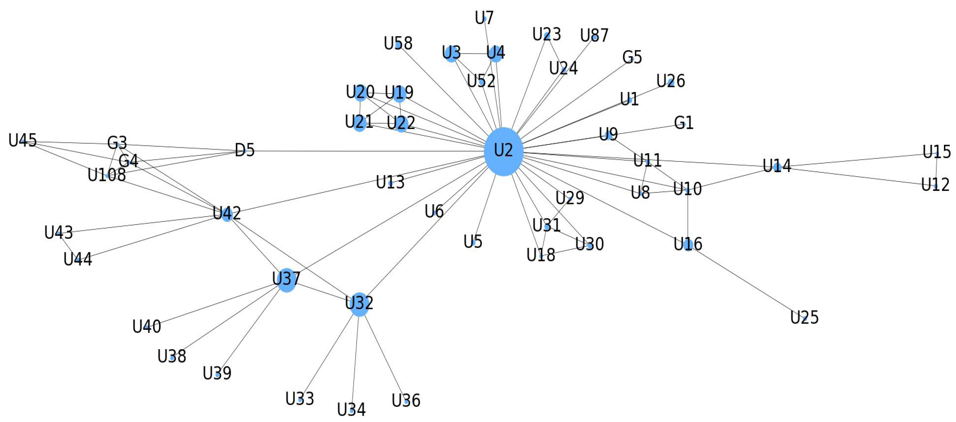
A netlist usually contains hundreds or thousands of components and connections, but it is usually of interest to ICs with more pins and important connections. In order to better view the connection relationship of each node in the entire netlist and analyze the functional structure of the entire netlist, it is necessary to visualize the netlist. Because the module partition is centered on the IC chip, in order to simplify the visualization of the netlist, only the connections between the IC chips in the netlist are considered. Among them, IC chips include memory chips, CPU, FPGA, power chip, DSP (digital signal processor), AD/DA, MCU (microcontroller), MEMS, active crystal oscillator, etc., as well as various customized SOCs. Our netlist visualization focuses on the topology structure obtained after ignoring power nets, GND nets, and other two-pin components and non-active multi-pin components in the netlist, and retaining the core components and core networks. The visual analysis of the netlist can highlight the dependencies between the core components in the netlist and inspire hierarchical module partition. As shown in Figure 1, the solid ellipse is the core component IC, and its size is proportional to the number of pins of the component, and the black solid line is the connection relationship. Components with more pins are in the center with close connection to the rest, and components with fewer pins are scattered around the edges of the graph. For example, in Figure 1, the largest U2 chip is an FPGA, the second largest, U32 and U37, are AD chips, and U3, U4, U19, U20, U21, and U22 are memory chips. Through such simplification for the netlist, it can be seen that the connection between IC and IC is a node-to-node association. Therefore, it can be considered to simplify the netlist into a plane graph instead of a hypergraph, which effectively reduces the complexity of netlist partition.
3.3. Circuit Pattern Analysis
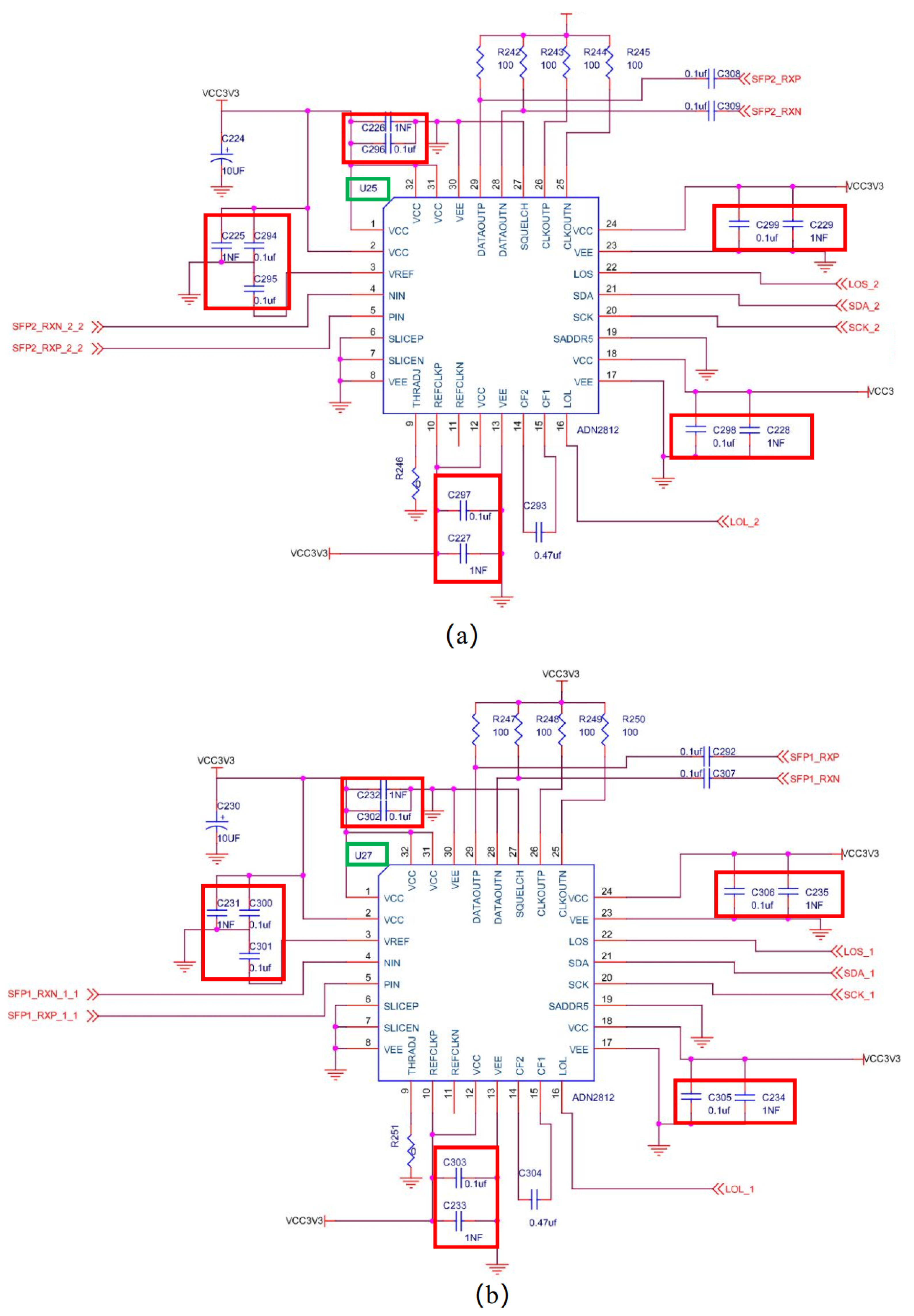
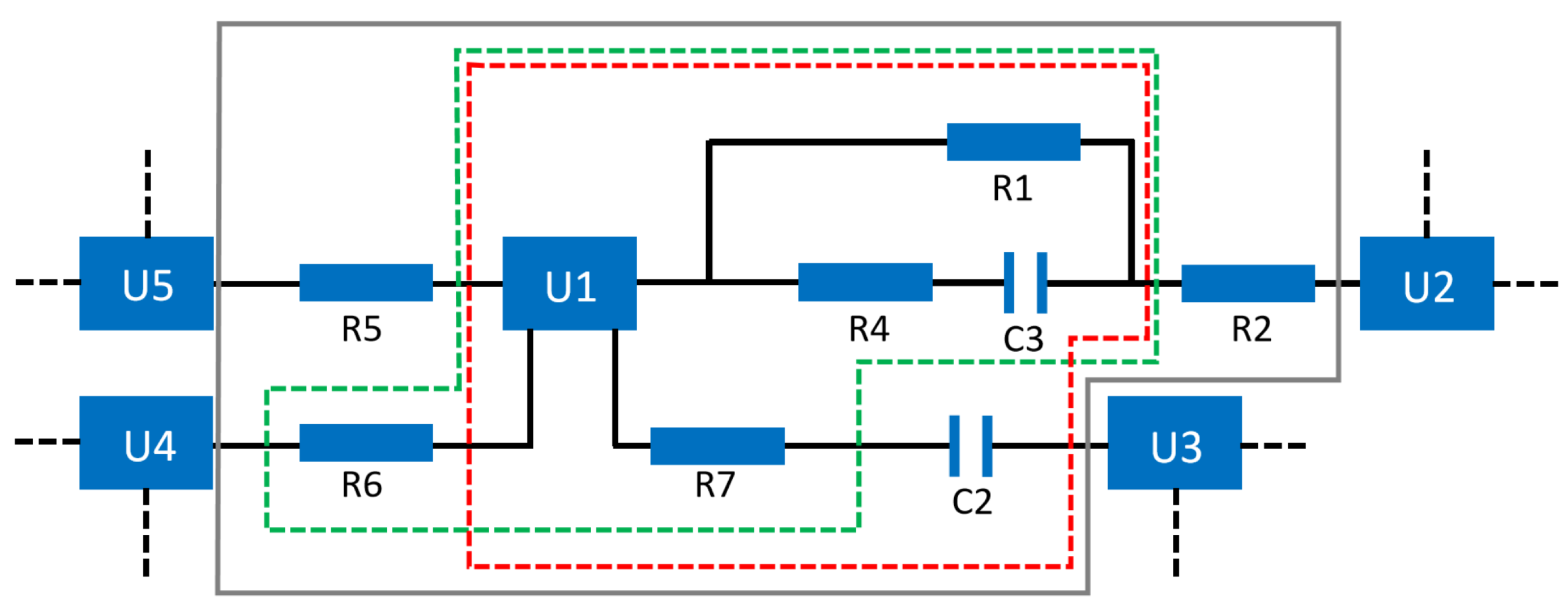
Repetitive pattern: It is also found that there are often many identical or similar modules in the netlist. First, from the netlist visualization, the same or similar modules can be roughly inferred based on the size of the circle representing the IC. Secondly, we can also find the same module from the connecting circuit around each IC. The surrounding circuits of these same modules are not only partitioned the same, but the layout and routing can also be reused; see Figure 2. There are so many cases where the same submodule appears in the netlist. We give the statistics of the same modules in 11 netlists to show the importance of repetitive pattern recognition in Section 5.1. This pattern will be used later by the netlist partition method.
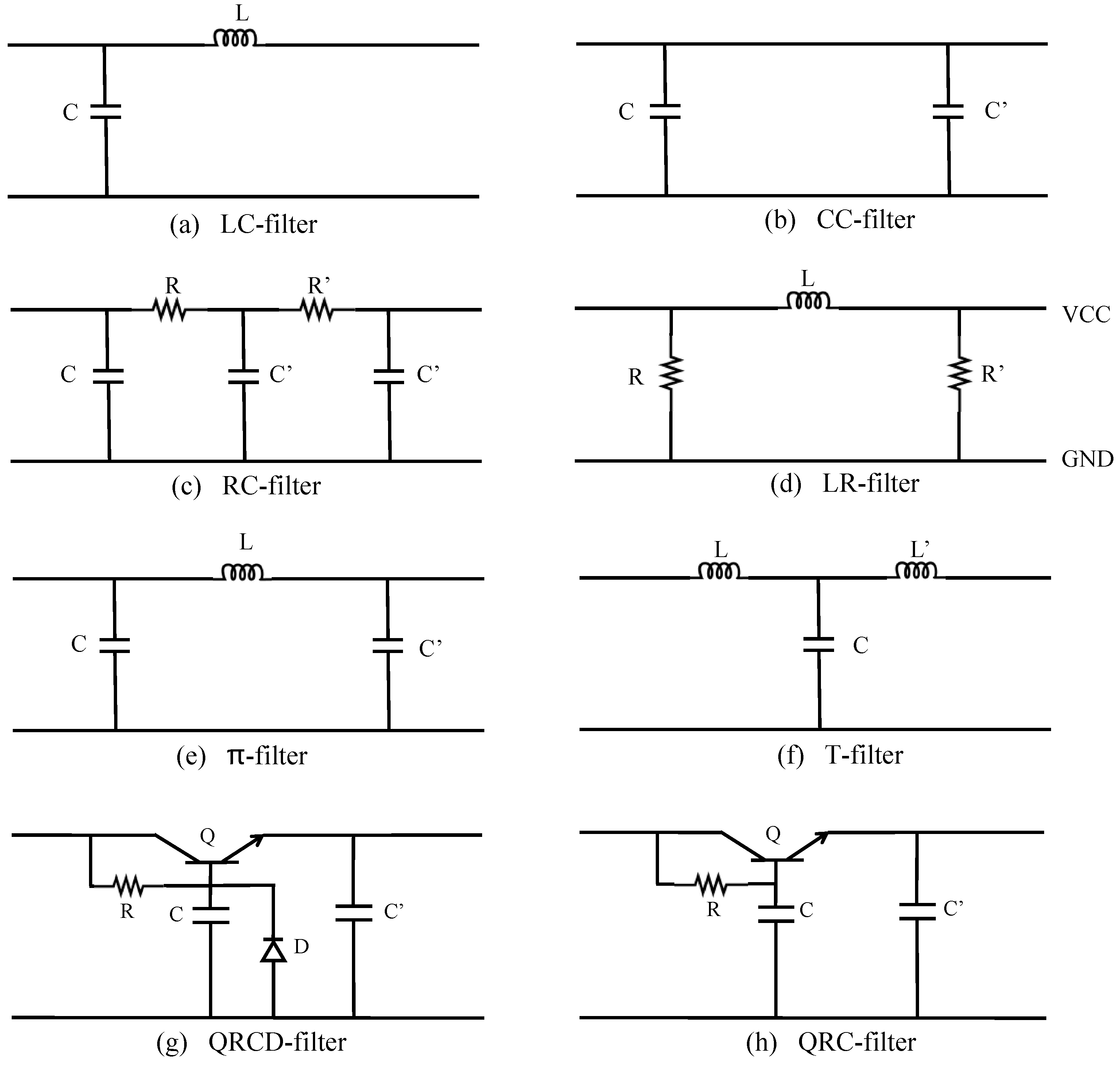
Generic circuit pattern: There are many generic circuit patterns in both digital and analog circuits. Here, we take the filtering circuit for example. The voltage output by the rectifier circuit is a one-way pulsating voltage that cannot be used directly for the electronic circuit. Therefore, the output voltage should be filtered to eliminate the alternating current (AC) component in the voltage, and then it will be used by the electronic circuit after becoming direct current (DC). In the filter circuit, components with special impedance characteristics to AC are mainly used, such as capacitors and inductors. Therefore, there are some fixed circuit structures to filter various electrical signals. Different filtering processes have different characteristics and adapt to different situations. As shown in Figure 3, there are eight kinds of filter circuits, in which R represents resistance, C represents capacitance, L represents inductance, Q represents triode, and D represents diode. These fixed circuit structures are summarized and become fixed patterns. These patterns are not explicit in the netlist, but require to be further discovered. If these fixed patterns can be discovered from the netlist, it would be very useful undoubtedly for the design of circuit partitioning algorithms.
4. Circuit Partitioning Based on Net Attributes and Patterns
In this section, we introduce the proposed method in detail. First, ICs are selected as key components, and the partition sets are initialized by cutting the attribute networks. Scattered components are allocated by classifying, matching, and force according to different circuit patterns.
4.1. Key Component Selecting and Initial Partitioning
As the development of circuit design technology progresses, the standardization of circuit design becomes better. It is observed that the nets are always specified by keywords. These keywords could help engineers to examine the information source flow. As mentioned in Section 3.1, networks include signal network, clock network, power network, and GND network. The data network generally includes keywords such as DATA and D, and some communication protocols, such as SPI and I2C, also belong to data networks. The address network generally includes keywords such as ADRESS, A, and Add, and the clock network generally includes CLOCK, CLK, CK; the power network mainly provides power for the components, generally including VCC, VDD, VEE, VPPPOWER; GND represents the ground network. When engineers design circuits, they often label important nets, called net attributes. The net attributes help us to discover the logical structure in netlists, and inspire us to propose the system initial partition based on net attributes.
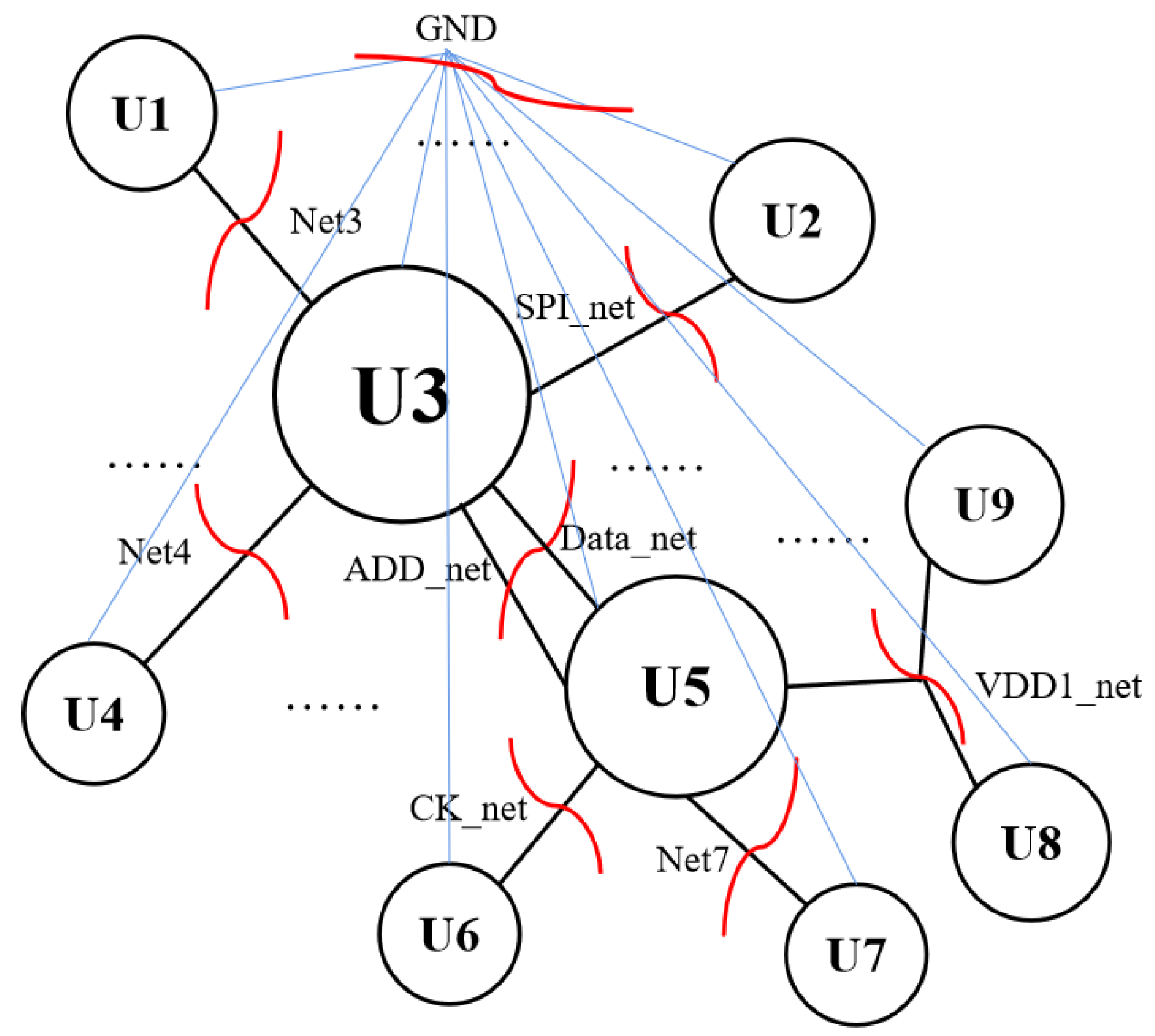
First, we select ICs as key components, for which the most characteristic is that the number of pins are greater than three. A network usually connects multiple IC modules. Each module centers around an IC chip, and many components are connected to serve the IC chip, which should belong to the module. Cutting off the attribute network can form a natural and basic module partition, as shown in Figure 4. Since these components are closely related to the IC chip, there is no significant network attribute labeling on the connection relationship, so they will be automatically divided into the IC module. Assuming that each IC chip is the center, initial partition subsets, denoted by , are formed by cutting important networks, which include the closely related components around them. It is noted that the number of pins of junctors and multi-pin switches are also more than three, but they are ignored in our algorithm since they are passive components and cannot be the center of modules.
4.2. Scattered Components Description
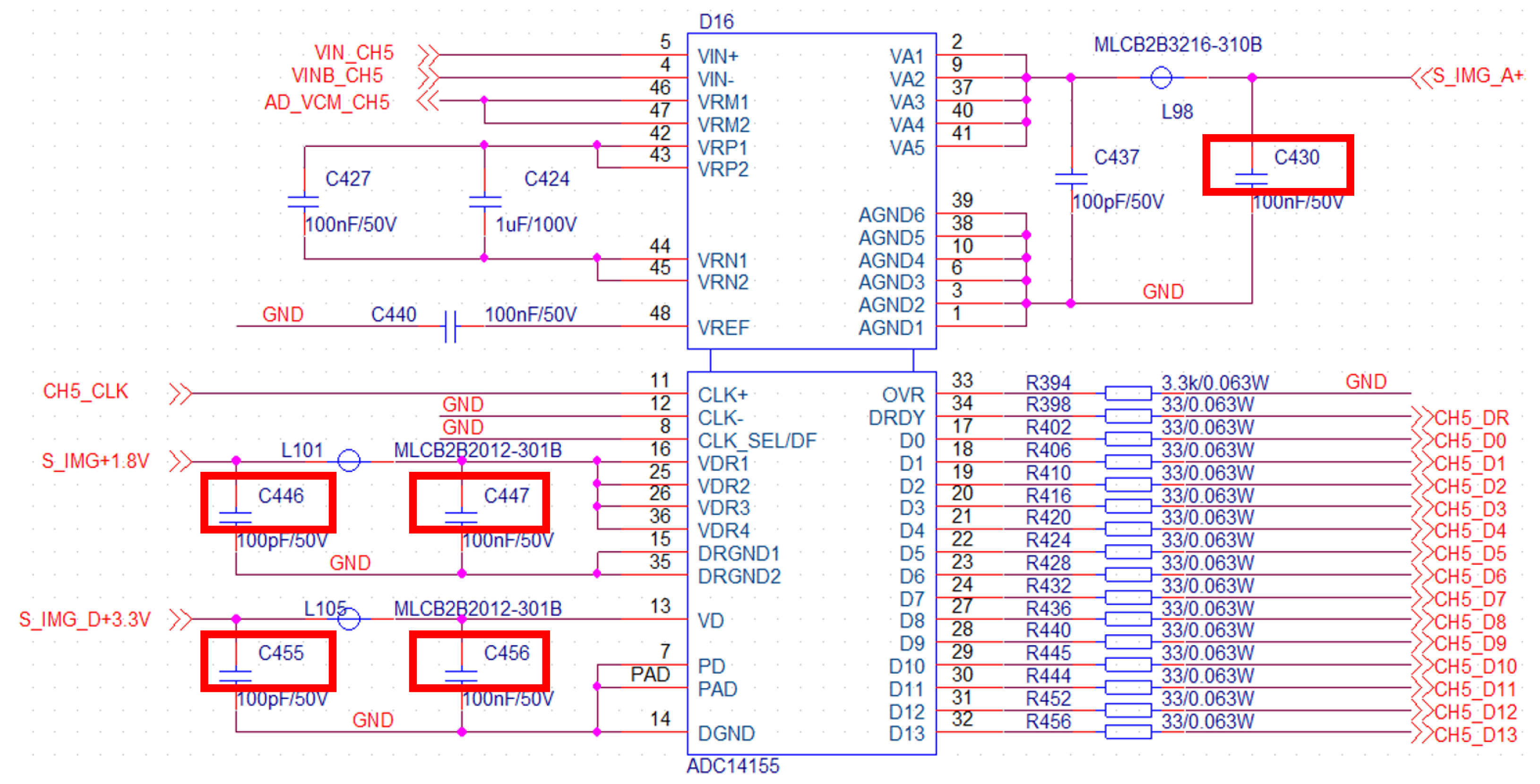
Unfortunately, some components that are between important networks will be scattered without affiliation to any subset of the IC chip. As shown in Figure 5, scattered components, for example, capacitors C455 and C456, are located between the power supply network and GND. When the important networks are cut, C455 and C456 are scattered because they could belong to any module, similar to C456, C447, and C430. The problem is that we do not know the affiliation for these capacitors just from the netlist; however, some clues are found from the schematic diagram of circuits. Let , , represent the sets of signal net, power supply net, and GND net, respectively. We summarize the scattered components into the following categories:
- (1)
- Components scattered between signal network and signal network , denoted by .
- (2)
- Components scattered between signal network and power supply network denoted by .
- (3)
- Components scattered between signal network and GND ground network , denoted by .
- (4)
- Components scattered between power network and GND ground network , denoted by .
In actuality, the cases would be more complicated, because , , , and could have intersection. Here, we just simplify the description. Scattered components in the netlists mainly include capacitors, resistors, inductors, and others. The numbers of capacitors and resistors are the most. Capacitors between the power network and GND network mainly play four roles: filtering, voltage regulation, energy storage, and bypass energy storage, while resistors mainly play the role of bleeder resistance effect. Assuming that the scattered components between the mth net and the nth net are adjacent, denoted by , we introduce three rules to perform assignment of these scattered components to modules.
4.3. Scattered Components Allocation by Classifying
It can be observed from some circuit schematic diagrams those that have been designed by human: according to the design habits of engineers, the resistors and capacitors in the same module are usually named similarly or closed. As shown in Figure 5, the scattered components can be allocated by nearest neighbor classifier due to the special circuit structure. Let be the candidate set to be allocated, which connects multiple IC module sets . Let represent the pth component to be allocated between the net and by matching with the nearest neighbor method. is short for which represents the distance between the component and the subset , and it is calculated according to the string of scattered components. We summarize the allocated Rule (1) as follows:
in which refers to the closest set between the component and the subsets , , and . is the threshold set in advance.
4.4. Scattered Components Allocating by Force
If there still exists some components un-allocated between two nets and , they will be allocated by force, which is heuristic. So far, each module set contains a certain number of components. It is observed that the bigger IC modules have more capability to host the rest components. Assume the module set has components in it, which determines the force to attract the rest of the component. They can be allocated by Rule (2) as follows:
in which are connected modules by a certain net. The magnitude of force F is proportional to the number of components in the module set. The bigger the number of components, the greater the force.
4.5. Scattered Components Allocating by Module Matching
It is observed that a netlist always contains many of the same modules, and then they have the same electrical specification; see Figure 2. If some scattered components are located between two or multiple IC chip modules, which are the same or closed modules, then the peripheral circuits of the same IC module are almost the same. Thus, it is reasonable to think that the surrounding components are also the same. If the parameters of the scattered components among them are the same, they should be evenly allocated to these closed or the same multiple IC modules. Therefore, we first detect IC chips if they are closed or the same on an individual important network through IC parameters. These parameters include the number of pins and the statistics in the module set such as the number of capacitors, resistors, inductors, others, and volume.
Let be a feature function of IC modules . represents the parameters function of the scattered component including type and volume, in which refers to the rest components between net and after the first round of allocation by Rules (1) and (2). Assume , and is a subset in which the modules are closed or the same from . We summarize the allocating Rule (3) as follows:
where is the set of candidate components to be allocated, is the set of candidate subsets, and are the cardinality of the set and , respectively. is the set of natural numbers, is the threshold set in advance.
4.6. The Proposed Algorithm
We summarize the whole algorithm in Algorithm 1. Our method requires a PCB netlist and thresholds and as input, and takes the PCB netlist partition sets as output. and are two thresholds which need to be set in advance. is a tuning parameter and is empirically set. We set less than five through our experiments. Each component has to be allocated to a certain partition subset, and every subset has one IC as the center since all resistors, capacitors, inductors, transistors, and other non-IC components are supposed to serve the IC. Of course, some connectors and switches may be independent functionally; they are allocated to the nearest module through our algorithm. Partition initial sets are obtained in Section 4.1. Rules (1), (2), and (3) are explained in Section 4.3, Section 4.5 and Section 4.4, respectively. refer to the sets connected to , respectively, and they are denoted as follows:
is the number of nets connected to power nets and GND net. Since our algorithm is heuristic, the time complexity is quite low compared with graph cut algorithms. The time complexity of the initial partition is , and the time complexity of the second part—allocating scattered components by Rules (1)–(3)—is , where K is the number of components.
| Algorithm 1 The algorithm of circuit partitioning for PCB netlist based on net attributes |
| Require: a PCB netlist with K components, the thresholds ,; Ensure: PCB partition sets ; Select IC as key components; Obtain Partition initial sets as in Section 4.1; /*Allocating scattered components by Rule (1);*/—Stage 1 repeat select one element from ; Check module subsets of connected; If Then ; ; until . /*Allocating scattered components by Rule (2);*/—Stage 2 if repeat select one element from ; Check module subsets of connected; If Then ; ; endif until ; endif /*Allocating scattered components by Rule (3);*/—Stage 3 ; repeat select one net from ; ; Check module subsets of connected, and components in ; If , ; s. t. , Then Allocate them equally; Else Allocate them roughly equally; until . |
5. Experimental Results
In the experimental section, we introduce our datasets and evaluation indices, and analyze comparison results.
5.1. Datasets
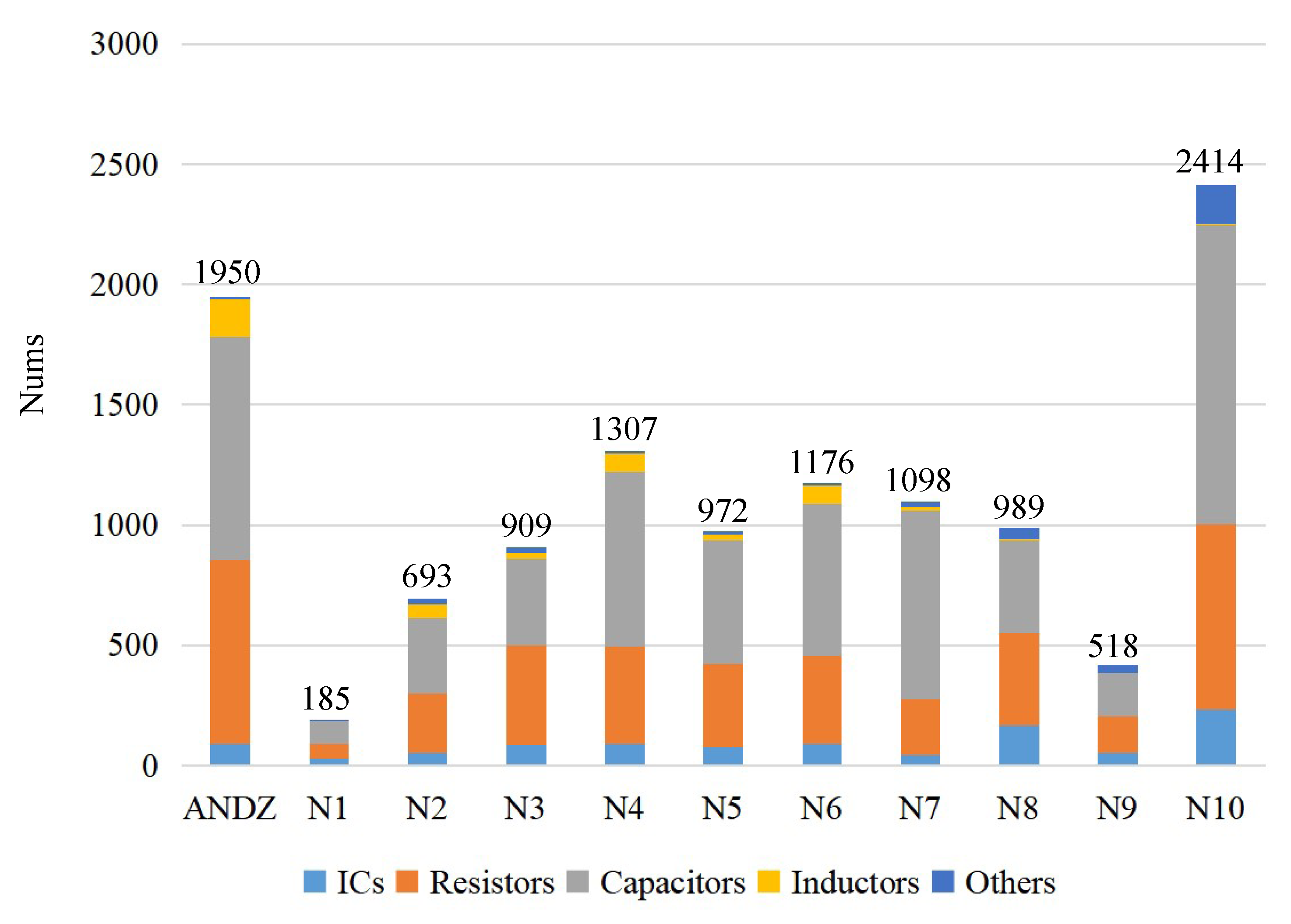
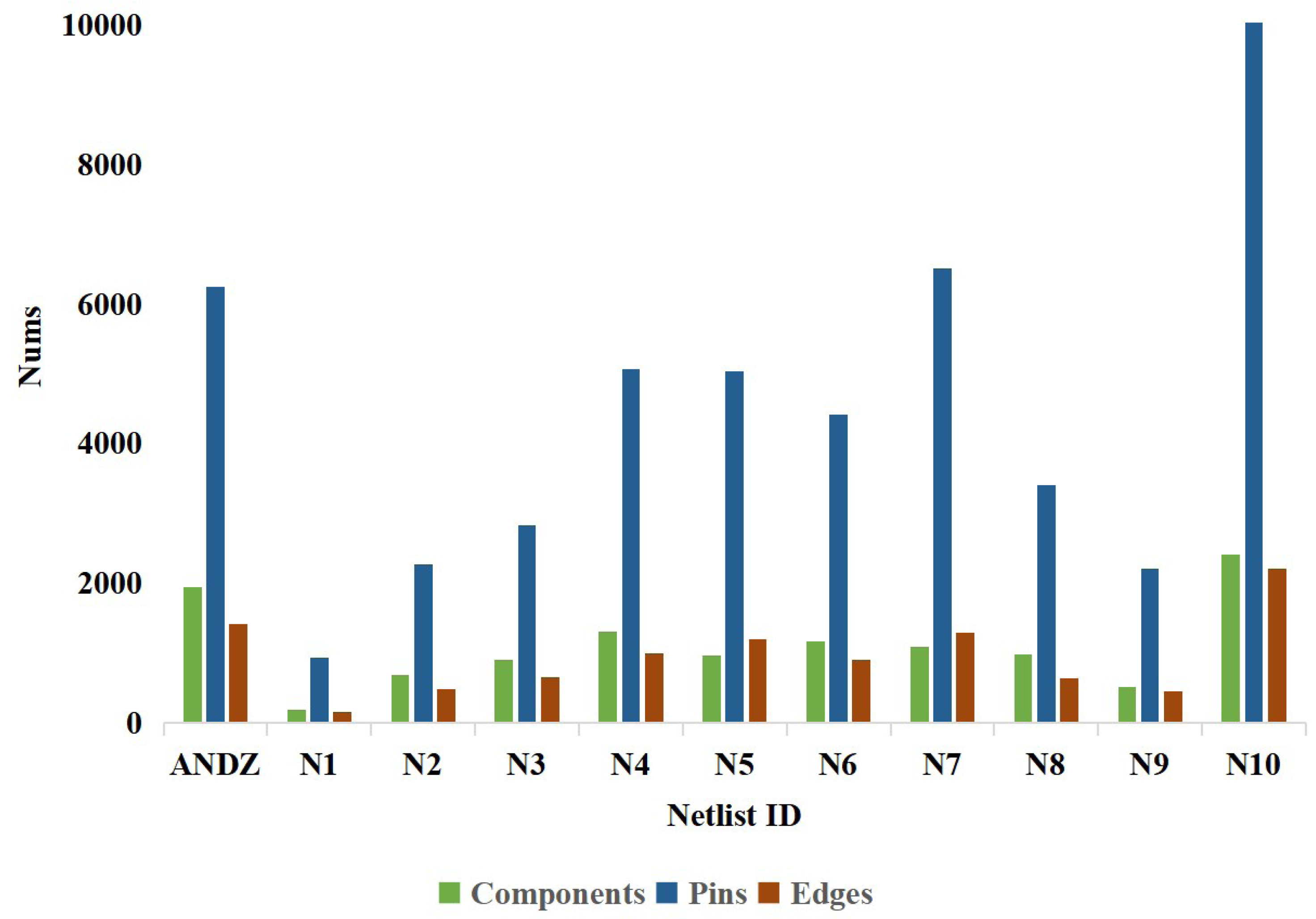
Since few netlist datasets are public, we build 11 PCB netlist datasets and partition the netlists into subsets manually. The number of components in 11 netlists is from dozens to , and the total number of pins in netlists is from hundreds to tens of thousands. In addition to IC chips, there are mainly resistors and capacitors, which account for more than of the total number of components, so that the scattered components are mainly resistors and capacitors. The statistics of resistors, capacitors, and inductors are shown in Figure 6, and the statistics of components, pins, and edges for the PCB netlist datasets are shown in Figure 7. We also report the total number of subsets in our datasets, and make statistics for the same modules in each netlist, which are shown from the third column to the twelfth column in Table 1. It can be seen that each netlist has multiple same modules. We test the proposed algorithm on the netlist datasets.
5.2. Evaluation Indices
Since the netlist partition is treated as a segmentation-like problem, the evaluation indices are borrowed from the image processing field. We compute partition accuracy (ACC), Dice similarity coefficient (Dice), intersection over union (IOU), sensitivity (SE), and precision (PR). These evaluation indices are computed from true positive (TP), true negative (TN), false positive (FP), and false negative (FN) [27]. Figure 8 shows how to compute TP, TN, FP, and FN in our case, in which
The ground truth set is in the green block, the partition set from the proposed method is in the red block, and components set in the gray block are the whole possible set.
A is the ground truth set, B is the partition set, C is the whole candidate set, and A, B, and C are shown in Figure 8. Since we have multiple partition subsets in each netlist, the final evaluation is a weighted index through all subsets. The equation expression is as follows:
in which N is the number of partition sets obtained from the method, is the ith partition subset, is the whole set, and = [ACC, Dice, IOU, SE, PR] is the score vector for the ith partition subset.
5.3. Comparison Results
We compare our method with the MaxFlow algorithm [10]. The MaxFlow algorithm is a popular method for graph cut. We report the comparison results in Table 2. It can be seen that our proposed algorithm can achieve 82.8–96.8% on partition accuracy, 80.2–93.0% on Dice, 72.9–89.5% on IOU, 80.6–94.2% on SE, and 79.8–93.9% on precision, while MaxFlow only has 11.4–39.2% on partition accuracy, 15.2–68.5% on Dice, 10.4–59.4% on IOU, 19.4–55.8% on sensitivity, and 12.5–63.6% on precision. This is because the MaxFlow method only considers the geometric attributes, while our method considers not only the geometric connection but also the circuit network attributes, and discovers the potential patterns to help partition algorithm, so it outperforms the MaxFlow algorithm significantly through all netlist datasets. Especially for N2, N3, N4, N5, and N6, netlists that have more than 100 subsets, the partition results from our method are also as good as those netlists that have fewer than 100 subsets, such as ANDZ, N1, N7, N8, N9, and N10. That means our proposed method is universal for the datasets and can be applied to different netlists.
6. Discussion
We also analyze the three rules proposed in this paper, and report results on Stage 1, Stage 2, and Stage 3 of the algorithm in terms of ACC, Dice, IOU, SE, and PR in Table 3. The scattered components in are allocated by Rule (1) in the first stage, and the rest of the components in are allocated by Rule (3). The scattered components in are allocated by Rule (2). Rule (1) is useful for the components allocated between signal net and power net, and between signal nets. Rule (2) is useful to allocate the scattered components between power nets and GND net, which are usually repetitive modules. It can be seen that the results are improved one by one from Stage 1 to Stage 3, which means that the three rules summarized from our observation are meaningful. Rule (2) significantly improves the results from Stage 2 to Stage 3. It shows that a lot of repetitive modules exist in netlists. Even with a simple pattern discovered, the partition results are improved a lot.
7. Conclusions
In this paper we analyzed the potential features in netlists through visualization, and proposed a partition algorithm with consideration of net attributes and potential patterns in circuits for PCB netlists. We extracted the net attributes from netlist first, and initially partitioned netlists. Three rules were discovered from our observation of special circuit structures. The proposed algorithm is a heuristic approach. Compared with other existing heuristic methods, our approach tries to discover the potential patterns in the netlists. The proposed algorithm outperforms the MaxFlow algorithm which is a graph cut method in the evaluation indices of accuracy, Dice, IOU, SE, and PR. In the future work, more potential circuit patterns will be studied, and they will provide more clues for module partitioning.
Author Contributions
Conceptualization, Y.Z. and L.B.; methodology, Y.Z. and D.M.; software, D.M.; validation, Y.Z. and D.M.; formal analysis, Y.Z. and D.M.; investigation, Y.Z.; resources, Y.Z.; data curation, D.M.; writing—original draft preparation, Y.Z.; writing—review and editing, Y.Z. and L.B.; visualization, D.M.; supervision, Y.Z. and L.B.; project administration, Y.Z. and L.B.; funding acquisition, Y.Z. and L.B. All authors have read and agreed to the published version of the manuscript.
Funding
This research was funded by the National Natural Science Foundation of China (NSFC No. 61971106).
Institutional Review Board Statement
Not applicable.
Informed Consent Statement
Not applicable.
Data Availability Statement
Not applicable.
Acknowledgments
The authors express their sincere appreciation and profound gratitude to Jian Yang (JUJN TECH Company Limited) for his valuable suggestions and paper proofing, and to research assistants Pingyou Jia and Hongtao Jiao for data collection.
Conflicts of Interest
The authors declare no conflict of interest.
References
- Kernighan, B.W.; Lin, S. An efficient heuristic procedure for partitioning graphs. Bell Syst. Tech. J. 1970, 49, 291–307. [Google Scholar] [CrossRef]
- Kahng, B.K.; Lienig, L.; Markov, I.L. VLSI Physical Design: From Graph Partitioning to Timing Closure; Springer: Berlin/Heidelberg, Germany, 2011. [Google Scholar]
- Karypis, G.; Aggarwal, R.; Kumar, V.; Shekhar, S. Multilevel hypergraph partitioning: Applications in VLSI domain. IEEE Trans. Very Large Scale Integr. (VLSI) Syst. 1999, 7, 69–79. [Google Scholar] [CrossRef]
- Caldwell, A.E.; Kahng, A.B.; Markov, I.L. Design and implementation of move-based heuristics for VLSI hypergraph partitioning. J. Exp. Algorithmics (JEA) 2000, 5, 5-es. [Google Scholar] [CrossRef]
- Meng, D.; Zheng, Y.L. Circuit Partitioning for PCB Netlist Based on Net Attributes. In Proceedings of the International Conference on Machine Learning and Cybernetics, Toyama, Japan, 9–11 September 2022. [Google Scholar]
- Barnes, E.R. An algorithm for partitioning the nodes of a graph. Algebr. Discret. Methods Siam J. 1982, 3, 541–550. [Google Scholar] [CrossRef]
- Nayak, S.; Panda, S.; Panda, M. Circuit Partitioning optimization using Parallel refinement algorithm. In Proceedings of the International Conference on Applied Electromagnetics, Signal Processing and Communication (AESPC), Bhubaneswar, India, 22–24 October 2018. [Google Scholar]
- Ford, L.R.; Fulkerson, D.R. Flows in Networks; Princeton University Press: Princeton, NJ, USA, 1962; p. 11. [Google Scholar]
- Liu, L.T.; Kuo, M.T.; Cheng, C.K.; Hu, T.C. A replication cut for two-way partitioning. IEEE Trans. Comput.-Aided Des. Integr. Circuits Syst. 1995, 14, 623–630. [Google Scholar]
- Boykov, Y.; Kolmogorov, V. An experimental comparison of min-cut/max-flow algorithms for energy minimization in vision. IEEE Trans. Pattern Anal. Mach. Intell. 2004, 26, 1124–1137. [Google Scholar] [CrossRef]
- Hamada, T.; Cheng, C.K.; Chau, P.M. An efficient multilevel placement technique using hierarchical partition. In Proceedings of the IEEE International Sympoisum on Circuits and Systems, Singapore, 11–14 June 1991. [Google Scholar]
- Areibi, S.; Vannelli, A. An efficient clustering technique for circuit partitioning. In Proceedings of the IEEE International Symposium on Circuits and Systems. Circuits and Systems Connecting the World (ISCAS), Atlanta, GA, USA, 12–15 May 1996. [Google Scholar]
- Hadley, S.W.; Mark, B.L.; Vannelli, A. An efficient eigenvector approach for finding netlist partitions. IEEE Trans. Comput.-Aided Des. Integr. Circuits Syst. 1992, 11, 885–892. [Google Scholar] [CrossRef]
- Fiduccia, C.M.; Mattheyses, R.M. A linear-time heuristic for improving network partitionse. In Proceedings of the Design Automation Conference, Las Vegas, NV, USA, 14–16 June 1982; pp. 175–181. [Google Scholar]
- Sinha, B.; Laskar, N.M.; Sen, R.; Baishnab, K.L. Heuristics in Physical Design Partitioning: A Review. In Proceedings of the IEEE International Conference on Innovations in Information Embedded and Communication Systems (ICIIECS), Coimbatore, India, 19–20 March 2015. [Google Scholar]
- Yeh, C.W.; Cheng, C.K.; Lin, T.T. A general purpose, multiple-way partitioning algorithm. IEEE Trans. Comput.-Aided Des. Integr. Circuits Syst. 1994, 13, 1480–1488. [Google Scholar]
- Cong, J.; Lim, S.L. Edge Separability-Based Circuit Clustering With Application to Multilevel Circuit Partitioning. IEEE Trans. Comput.-Aided Des. Integr. Circuits Syst. 2004, 23, 346–357. [Google Scholar] [CrossRef]
- Cherng, J.S.; Chen, S.J. An efficient multilevel partitioning algorithm for VLSI circuits. In Proceedings of the IEEE International Conference on VLSI Design, New Delhi, India, 4–8 January 2003. [Google Scholar]
- Manna, K.; Choubey, V.; Chattopadhyay, S.; Sengupta, I. Thermal variance-aware application mapping for mesh based network-on-chip design using Kernighan-Lin partitioning. In Proceedings of the International Conference on Parallel, Distributed and Grid Computing, Solan, India, 11–13 December 2014; pp. 274–279. [Google Scholar]
- Rajan, A.K.; Bhaiya, D. VLSI partitioning using parallel kernighan lin algorithm. In Proceedings of the International Conference on Communication and Signal Processing (ICCSP), Chennai, India, 6–8 April 2017; pp. 1897–1901. [Google Scholar]
- Manna, K.; Teja, V.S.; Chattopadhyay, S.; Sengupta, I. TSV Placement and Core Mapping for 3D Mesh Based Network-on-Chip Design Using Extended Kernighan-Lin Partitioning. ACM Trans. Embed. Comput. Syst. (TECS) 2016, 16, 1–25. [Google Scholar] [CrossRef]
- Lei, X.; Liang, W.; Li, K.C.; Luo, H.; Hu, L.; Cai, J.; Li, Y. A New Multilevel Circuit Partitioning Algorithm Based on the Improved KL Algorithm. In Proceedings of the IEEE International Conference on Big Data Security on Cloud (BigDataSecurity), Washington, DC, USA, 27–29 May 2019. [Google Scholar]
- Wei, Y.; Cheng, C.K. Ratio cut partitioning for hierarchical designs. IEEE Trans. Comput.-Aided Des. Integr. Circuits Syst. 1991, 10, 911–921. [Google Scholar] [CrossRef]
- Desai, S.M.; Gambhi, S.; Sharma, P. An Improved and Optimized Layer Assignment Partitioning Algorithm. In Proceedings of the IEEE International Conference Cloud System and Big Data Engineering, Noida, India, 14–15 January 2016. [Google Scholar]
- Panth, S.; Member, S.; Samadi, K.; Du, Y.; Lim, S.K. Placement-Driven Partitioning for Congestion Mitigation in Monolithic 3D IC Designs. IEEE Trans. Comput.-Aided Des. Integr. Circuit Syst. 2015, 34, 540–553. [Google Scholar] [CrossRef]
- Hu, L.R.; Duan, Q.; Qi, Z.; Wang, J.; Lai, J.M.; Yang, M. A new hyper-graph partitioning for 3D-FPGA. In Proceedings of the IEEE International Conference on Solid-State and Integrated Circuit Technology (ICSICT), Qingdao, China, 31 October–3 November 2018. [Google Scholar]
- Zhou, Z.H. Machine Learning; Tsinghua University Press: Beijing, China, 2016. [Google Scholar]
Figure 1.
Schematic diagram for initial partitioning by cutting important attribute networks.

Figure 2.
Repetitive pattern. Panels (a,b) are two of the same IC modules from a single netlist, U25 and U27, in green blocks. The capacitors in red blocks between the power net and GND net are scattered, and would be allocated equally by IC module matching in Section 4.5.
Figure 2.
Repetitive pattern. Panels (a,b) are two of the same IC modules from a single netlist, U25 and U27, in green blocks. The capacitors in red blocks between the power net and GND net are scattered, and would be allocated equally by IC module matching in Section 4.5.

Figure 3.
Eight different structures of filtering.

Figure 4.
Schematic diagram for initial partitioning by cutting important attribute networks, better viewed in color.
Figure 4.
Schematic diagram for initial partitioning by cutting important attribute networks, better viewed in color.

Figure 5.
The examples of scattered components in schematic diagram of the circuit. Components in red blocks are scattered after initial partition.
Figure 5.
The examples of scattered components in schematic diagram of the circuit. Components in red blocks are scattered after initial partition.

Figure 6.
The statistics of resistors, capacitors, inductors, and others for the datasets.

Figure 7.
The statistics of components, pins, and edges for the PCB netlist datasets.

Figure 8.
How to compute TP, FN, FP, and TN. Ground truth set A is in the green block, partition set B from the proposed method is in the red block, and components set in the gray block are the whole candidate set C. Better viewed in color. , , , .
Figure 8.
How to compute TP, FN, FP, and TN. Ground truth set A is in the green block, partition set B from the proposed method is in the red block, and components set in the gray block are the whole candidate set C. Better viewed in color. , , , .


Table 1.
The statistics of the number of subsets and repetitive modules in each netlist dataset.
| Netlist ID | No. of Subsets | No. of Same Modules | |||||||||
|---|---|---|---|---|---|---|---|---|---|---|---|
| 2 | 3 | 4 | 5 | 6 | 7 | 10 | 12 | 13 | 20 | ||
| ANDZ | 57 | 7 | 1 | 1 | 0 | 0 | 1 | 2 | 2 | 0 | 0 |
| N1 | 36 | 3 | 0 | 2 | 0 | 0 | 0 | 0 | 0 | 0 | 0 |
| N2 | 147 | 2 | 0 | 1 | 0 | 0 | 1 | 0 | 0 | 0 | 0 |
| N3 | 120 | 5 | 4 | 0 | 0 | 0 | 0 | 0 | 0 | 0 | 0 |
| N4 | 152 | 7 | 3 | 2 | 0 | 3 | 0 | 0 | 0 | 0 | 0 |
| N5 | 123 | 9 | 0 | 1 | 1 | 2 | 0 | 0 | 0 | 0 | 0 |
| N6 | 144 | 10 | 3 | 0 | 2 | 0 | 1 | 0 | 0 | 0 | 0 |
| N7 | 53 | 1 | 0 | 8 | 0 | 0 | 0 | 0 | 0 | 0 | 0 |
| N8 | 94 | 6 | 1 | 3 | 1 | 0 | 1 | 0 | 0 | 0 | 0 |
| N9 | 46 | 5 | 1 | 0 | 0 | 1 | 0 | 0 | 0 | 0 | 0 |
| N10 | 90 | 14 | 2 | 9 | 0 | 1 | 0 | 2 | 1 | 1 | 2 |
Table 2.
Comparison results. Results are compared with MaxFlow [10] in terms of ACC, Dice, IOU, SE, and PR.
Table 2.
Comparison results. Results are compared with MaxFlow [10] in terms of ACC, Dice, IOU, SE, and PR.
| Datasets | ACC | Dice | IOU | SE | PR | |||||
|---|---|---|---|---|---|---|---|---|---|---|
| MaxFlow | Ours | MaxFlow | Ours | MaxFlow | Ours | MaxFlow | Ours | MaxFlow | Ours | |
| ANDZ | 11.4 | 96.8 | 22.4 | 91.4 | 15.6 | 87.7 | 28.7 | 89.0 | 18.4 | 93.9 |
| N1 | 37.1 | 86.9 | 26.3 | 85.8 | 17.7 | 77.1 | 35.3 | 87.2 | 21.5 | 84.4 |
| N2 | 39.2 | 84.9 | 53.2 | 88.4 | 40.5 | 80.8 | 55.8 | 88.9 | 50.8 | 87.9 |
| N3 | 34.3 | 91.6 | 44.8 | 88.7 | 32.9 | 82.7 | 50.1 | 86.8 | 40.5 | 90.7 |
| N4 | 34.5 | 84.4 | 32.9 | 80.2 | 23.1 | 72.9 | 35.7 | 80.6 | 30.5 | 79.8 |
| N5 | 35.7 | 86.6 | 41.8 | 81.1 | 31.6 | 73.3 | 41.4 | 80.6 | 42.2 | 81.6 |
| N6 | 30.0 | 89.3 | 33.9 | 84.9 | 23.5 | 77.7 | 35.0 | 85.0 | 32.9 | 84.8 |
| N7 | 17.6 | 88.8 | 15.2 | 93.0 | 10.4 | 89.5 | 19.4 | 94.2 | 12.5 | 91.8 |
| N8 | 22.9 | 84.9 | 38.6 | 82.7 | 29.2 | 76.2 | 43.4 | 84.3 | 34.8 | 81.2 |
| N9 | 53.6 | 82.8 | 68.5 | 91.1 | 59.4 | 85.8 | 74.2 | 91.2 | 63.6 | 91.0 |
| N10 | 38.0 | 89.8 | 55.1 | 92.8 | 44.6 | 88.4 | 54.6 | 93.1 | 55.6 | 92.5 |
Table 3.
Comparison results on each stage in terms of ACC, Dice, IOU, SE, and PR. Each stage corresponds to each step in Algorithm 1.
Table 3.
Comparison results on each stage in terms of ACC, Dice, IOU, SE, and PR. Each stage corresponds to each step in Algorithm 1.
| Datasets | Stage 1 | Stage 2 | Stage 3 | ||||||||||||
|---|---|---|---|---|---|---|---|---|---|---|---|---|---|---|---|
| ACC | Dice | IOU | SE | PR | ACC | Dice | IOU | SE | PR | ACC | Dice | IOU | SE | PR | |
| ANDZ | 91.2 | 86.9 | 80.5 | 81.6 | 92.9 | 93.5 | 89.7 | 84.8 | 85.2 | 94.7 | 96.8 | 91.4 | 87.7 | 89.0 | 93.9 |
| N1 | 53.8 | 62.2 | 48.9 | 51.5 | 78.5 | 55.2 | 64.0 | 51.1 | 55.5 | 75.6 | 86.9 | 85.8 | 77.1 | 87.2 | 84.4 |
| N2 | 33.0 | 48.0 | 35.3 | 35.4 | 74.5 | 43.5 | 61.6 | 49.0 | 51.0 | 77.8 | 84.9 | 88.4 | 80.8 | 88.9 | 87.9 |
| N3 | 67.5 | 72.3 | 60.9 | 61.0 | 88.7 | 74.7 | 81.6 | 72.5 | 73.3 | 92.0 | 91.6 | 88.7 | 82.7 | 86.8 | 90.7 |
| N4 | 49.4 | 55.9 | 46.4 | 47.2 | 68.5 | 63.2 | 65.5 | 56.7 | 58.8 | 73.9 | 88.4 | 80.2 | 72.9 | 80.6 | 79.8 |
| N5 | 41.4 | 50.2 | 39.6 | 39.8 | 68.0 | 48.4 | 59.9 | 50.0 | 50.3 | 74.0 | 86.6 | 81.1 | 73.3 | 80.6 | 81.6 |
| N6 | 62.1 | 68.3 | 58.6 | 59.4 | 80.3 | 71.5 | 74.5 | 65.3 | 68.5 | 81.7 | 89.3 | 84.9 | 77.7 | 85.0 | 84.8 |
| N7 | 64.4 | 76.4 | 65.2 | 65.2 | 92.2 | 67.5 | 78.3 | 67.3 | 68.7 | 91.0 | 88.8 | 93.0 | 89.5 | 94.2 | 91.8 |
| N8 | 54.3 | 64.8 | 53.8 | 55.7 | 77.5 | 59.7 | 70.5 | 60.5 | 63.5 | 79.2 | 84.9 | 82.7 | 76.2 | 84.3 | 81.2 |
| N9 | 40.2 | 48.5 | 41.5 | 41.5 | 58.3 | 43.3 | 62.8 | 55.3 | 56.0 | 71.5 | 82.8 | 91.1 | 85.8 | 91.2 | 91.0 |
| N10 | 66.9 | 77.1 | 67.6 | 68.5 | 88.2 | 78.2 | 85.2 | 78.2 | 80.3 | 90.7 | 89.8 | 92.8 | 88.4 | 93.1 | 92.5 |
Publisher’s Note: MDPI stays neutral with regard to jurisdictional claims in published maps and institutional affiliations. |
© 2022 by the authors. Licensee MDPI, Basel, Switzerland. This article is an open access article distributed under the terms and conditions of the Creative Commons Attribution (CC BY) license (https://creativecommons.org/licenses/by/4.0/).
Share and Cite
MDPI and ACS Style
Zheng, Y.; Meng, D.; Bai, L. PCB Network Analysis for Circuit Partitioning. Appl. Sci. 2022, 12, 8200. https://0-doi-org.brum.beds.ac.uk/10.3390/app12168200
AMA Style
Zheng Y, Meng D, Bai L. PCB Network Analysis for Circuit Partitioning. Applied Sciences. 2022; 12(16):8200. https://0-doi-org.brum.beds.ac.uk/10.3390/app12168200
Chicago/Turabian StyleZheng, Yali, Da Meng, and Libing Bai. 2022. "PCB Network Analysis for Circuit Partitioning" Applied Sciences 12, no. 16: 8200. https://0-doi-org.brum.beds.ac.uk/10.3390/app12168200
Note that from the first issue of 2016, this journal uses article numbers instead of page numbers. See further details here.