Article

Correlating Disorder Microstructure and Magnetotransport of Carbon Nanowalls

by
Mijaela Acosta Gentoiu
1,
Rafael García Gutiérrez
2,
José Joaquín Alvarado Pulido
1,
Javier Montaño Peraza
2,
Marius Volmer
3,
Sorin Vizireanu
4,
Stefan Antohe
5,
Gheorghe Dinescu
4 and
Ricardo Alberto Rodriguez-Carvajal
6,*
1
Science Institute, Meritorious Autonomous University of Puebla, Puebla 72570, Mexico
2
Departamento de Investigación en Física, Universidad de Sonora, Hermosillo 83000, Mexico
3
Department of Electrical Engineering and Applied Physics, Transilvania University of Brasov, Blvd. Eroilor 29, 500036 Brasov, Romania
4
National Institute for Lasers, Plasma and Radiation Physics, 409 Atomistilor Street, Magurele, 077125 Bucharest, Romania
5
Faculty of Physics, University of Bucharest, 405 Atomistilor Street, 077125 Bucharest, Romania
6
Campus Guanajuato, Universidad de Guanajuato, Noria Alta S/N, Guanajuato 36250, Mexico
*
Author to whom correspondence should be addressed.
Submission received: 25 December 2022 / Revised: 3 February 2023 / Accepted: 6 February 2023 / Published: 14 February 2023

Abstract

:
The carbon nanowalls (CNWs) grown by Plasma-Enhanced CVD reveal differences in the magnetotransport properties depending on the synthesis parameters. In this paper, we report the influence of the deposition temperature, which produces variations of the disorder microstructure of the CNWs. Relative low disorder leads to the weak localization with the transition to weak antilocalization. Higher disorder generates positive Hopping mechanism in low field with a crossover to a diffusion transport by graphene nanocrystallites. The samples reveal a similitude of the isoline density of the MR at a low temperature (<50 K), explained in the context of the magnetization. This effect is independent of the number of defects. We can achieve a desirable amount of control over the MT properties changing the CNWs’ microstructure.

1. Introduction

The special magnetotransport (MT) properties of graphene-based nanostructures have received considerable attention in the last years. The uncommon Dirac point [1], chiral nature [2] and Berry’s phase [3] lead to different MT properties compared to the conventional two-dimensional (2D) systems. The graphene presents an unconventional weak antilocalization (WAL) due to the Berry’s phase π in a valley, which adds a quantum phase when two electron waves circulate in a reverse closed path, producing a suppression of backscattering [4]. The magnetotransport properties in graphene materials can be modified by the arrangement of sheets, particle size [5], disorder such as curvature, topological defects [6], geometry of the graphene edges, localized magnetic moment [7] and boundaries and interfaces [8].
Large 3D graphene networks, in contrast to 1D and 2D graphene-based nanostructures, easily allow us to modify the trajectories of carriers in a magnetic field to obtain a specific desirable MT behavior. There are not many studies related to the MT properties of 3D carbon nanowalls (CNWs), although these structures have other remarkable applications, such as catalyst supports, high sensitivity gas detection [9], biosensors [10] and super-capacitors [11,12]. Thus, completing the range of applications with those related to MT is a new direction for the exploration of the applicative potential of CNW materials. In MT research, we can mention Yue et al. [13], who obtained control over the magnetoresistance (MR) changing the morphology of the CNWs; and Huang et al. [14] in aligned walls.
The CNWs consist of stacks of a few vertical graphene layers in a self-supported network [15]. As a consequence, the sheets behave like freestanding ones [16], with a weak influence of the substrate. This advantage allows rigorously identify the intrinsic MT mechanism at difference of the graphene attached over a supporting substrate. Specifically, the quantum interference correction to the magnetotransport and the influences of the nature of disorder are currently lacking.
The deposition of CNWs is not straightforward and only a few methods are available. Zhang’s group [17] obtained the CNWs via RF sputtering, with the disadvantage of a long deposition time (3 h). Shang’s group [18], using the hot filament chemical vapor deposition (HFCVD) technique, needed catalysts or surface pretreatment. However, the Plasma-Enhanced Chemical Vapor Deposition (PECVD) is a typical and promising technique that does not require a catalyst [19] to grow with huge surface-to-mass ratio the CNWs [20] in a relatively low temperature (600–700 °C) and short time (~1 h). Davami et al. [21] stated that the deposition temperature is small compared to other synthesis methods, and numerous substrates (Ni, Ti, Pt, Cu, Ge, W, Ta, SiO2, Al2O3, Cu, Si, SiO2, stainless steel, carbon paper and others) can be used. Vizireanu et al. [22] showed that the morphology of CNWs does not change significantly when they are synthetized on substrates with different characteristics. In addition, the surface morphology and internal structure of the sample are effectively controlled.
The PECVD technique can generate CNWs with different morphologies (including petal-like, cauliflower-like and maze-like) depending on the deposition parameters, such as: temperatures and gaseous plasma (containing hydrogenated carbon precursors) [23]. The growth rate of CNWs (around tens of nanometers per minute) creates a difficulty for practical applications; however, Zhang et al. [23] improved it by increasing the RF power and CH4 flow rate. In this sense, the morphology and microstructure of the CNWs can be easily tunable through the PECVD method. In addition, CNWs could offer a new perspective for the reproducibility of MR devices, in contrast to the few-layer graphene grown by CVD, where the thickness is not controllable yet.
In this paper, it is presented a comparative study of the MT properties between two CNW samples differentiated by the disorder and grown by the PECVD technique. The selection of these two samples, named Sample I and Sample II, was made while considering the results of a structural and morphological comparative study between CNWs’ growth according to different synthesis parameters (time, Argon flux and deposition temperature ( T D )). The selected samples have structural and morphological qualities such as few graphene layers in the walls, large dimensions and a reduced contamination by hydrogen or oxygen atoms.
The disorder introduces mobility fluctuations in the magnetoresistance with the magnetic field applied. We find different magnetotransport effects as the disorder increases: weak localization and antilocalization caused by inherent defects or impurities (Sample I) and diffuse scattering from extrinsic electron scattering sites with Hopping magnetoresistance (Sample II). At a low temperature, the samples present a similar MR isoline density. The overall results could play significant roles in our understanding of the MT in graphene materials, as well as how to control the MT properties through tunable microstructure of the CNWs via the PECVD method. It leads new perspectives for magneto-electronic devices, including biosensors and magnetic field sensor [24], magnetoresistive random-access memories (MRAM), hard drives [25] and magneto-resistors for measuring electric current.

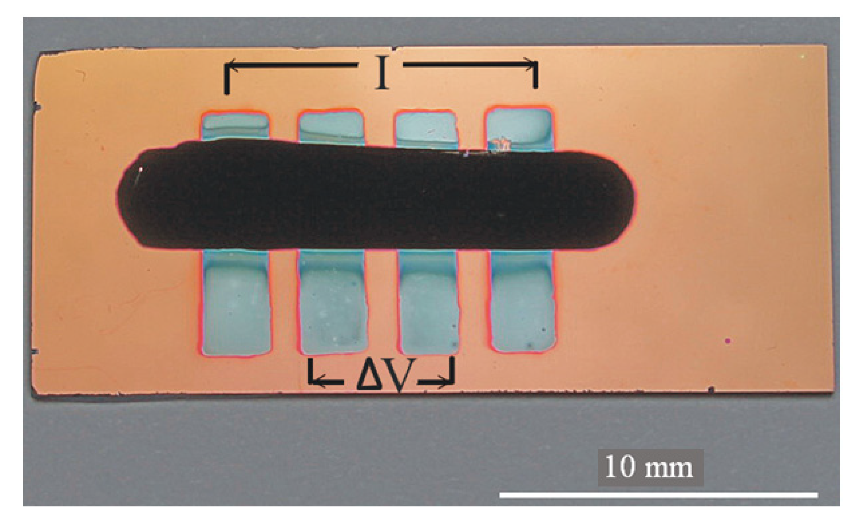
2. Experimental Section

Previous studies [26,27,28] have found the key to control different characteristics on the carbon nanowalls (such as length, shape and composition) through the synthesis parameters by the PECVD. We apply the following constant parameters: pressure of 120 Pa and RF power of 300 W, hydrogen/acetylene H2:C2H2 = 25:1 sccm and Si/SiO2 substrate placed at 5 cm from expansion nozzle. Table 1 shows the parameters that were varied: the ratio Argon flux at 1050 and 1400 sccm, the deposition time at 30 and 60 min, and the deposition temperature T D = 600   C and T D = 700   C . In the following, we named the samples formed at 1400 sccm-600 °C-1 h and 1400 sccm-700 °C-1 h Sample I and Sample II, respectively, due to the relevant structural and morphological characteristics to the magnetotransport studies.
The shape and the space between the walls of CNWs were observed by Scanning Electron Microscope (SEM), using an SEM 630 FEI Nova Nano at 10−4 mbar and Transmission Electron Microscope (TEM) with a JEOL 2010-F Field Emission of high resolution, operating at 200 kV. The Raman spectrum was obtained with a λ l a s e r = 632.8   nm , using a Horiba-Jobin-Yvon HR LabRAM. The Elastic Recoil Detection Analysis (ERDA) shows the hydrogen in-depth profile and concentration using 3MeV 4He2+ ions from a 3 MV Tandetron accelerator.
Figure 1 shows the configuration of the MR measurement, where the CNWs’ samples were synthetized on four consecutive chrome-gold electrodes. The metallic strips had a gap of around 1 mm. The spacing and length of the electrodes were chosen to study the MT across a large number of CNWs junctions. The MR measurements were performed by injecting a constant electric current of 5 mA (the high value was selected due to the elevated number of walls between the electrodes). The MR behavior was not clear with values that were too small (below 1 mA). An externally relatively high magnetic field B ranging from 0 to 7 T, perpendicular to the sample’s surface (parallel to the graphene layers), was applied. The temperature for measurements varied between 15 and 250 K. The MR was calculated as follows:
M R = R B R ( 0 ) R ( 0 ) · 100 %
where R(B) is the resistance with the magnetic field applied, while R(0) is the resistance in the absence of magnetic field.

3. Results and Discussion

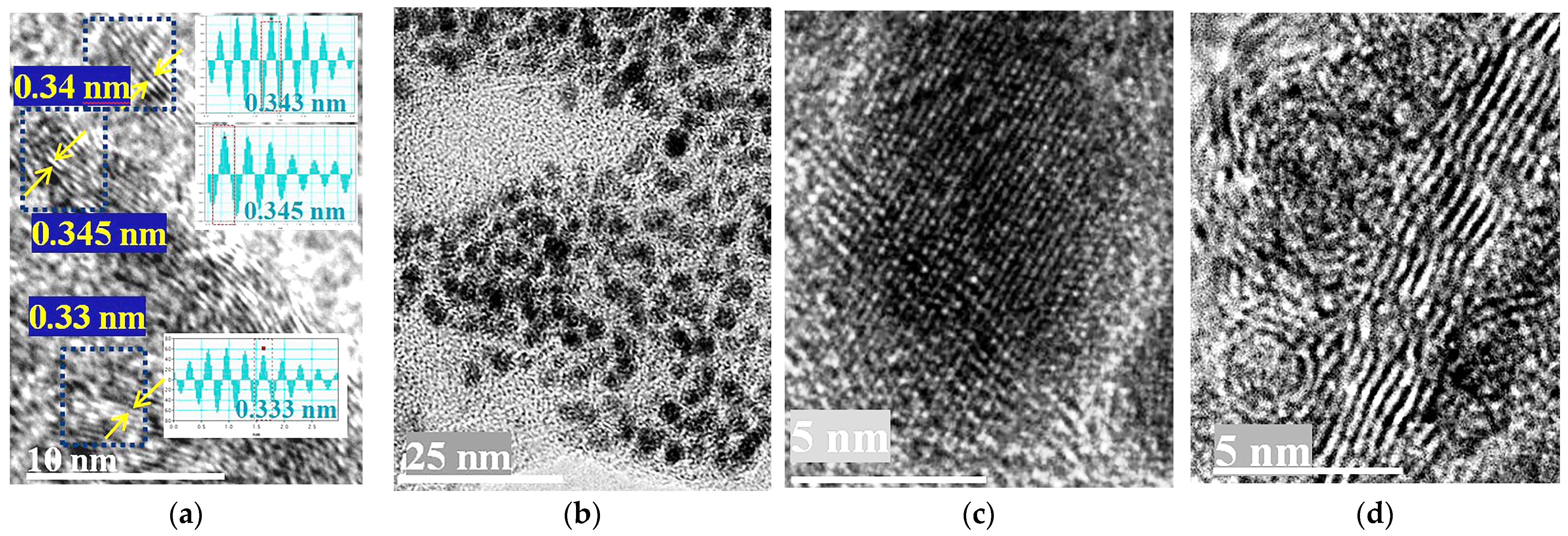
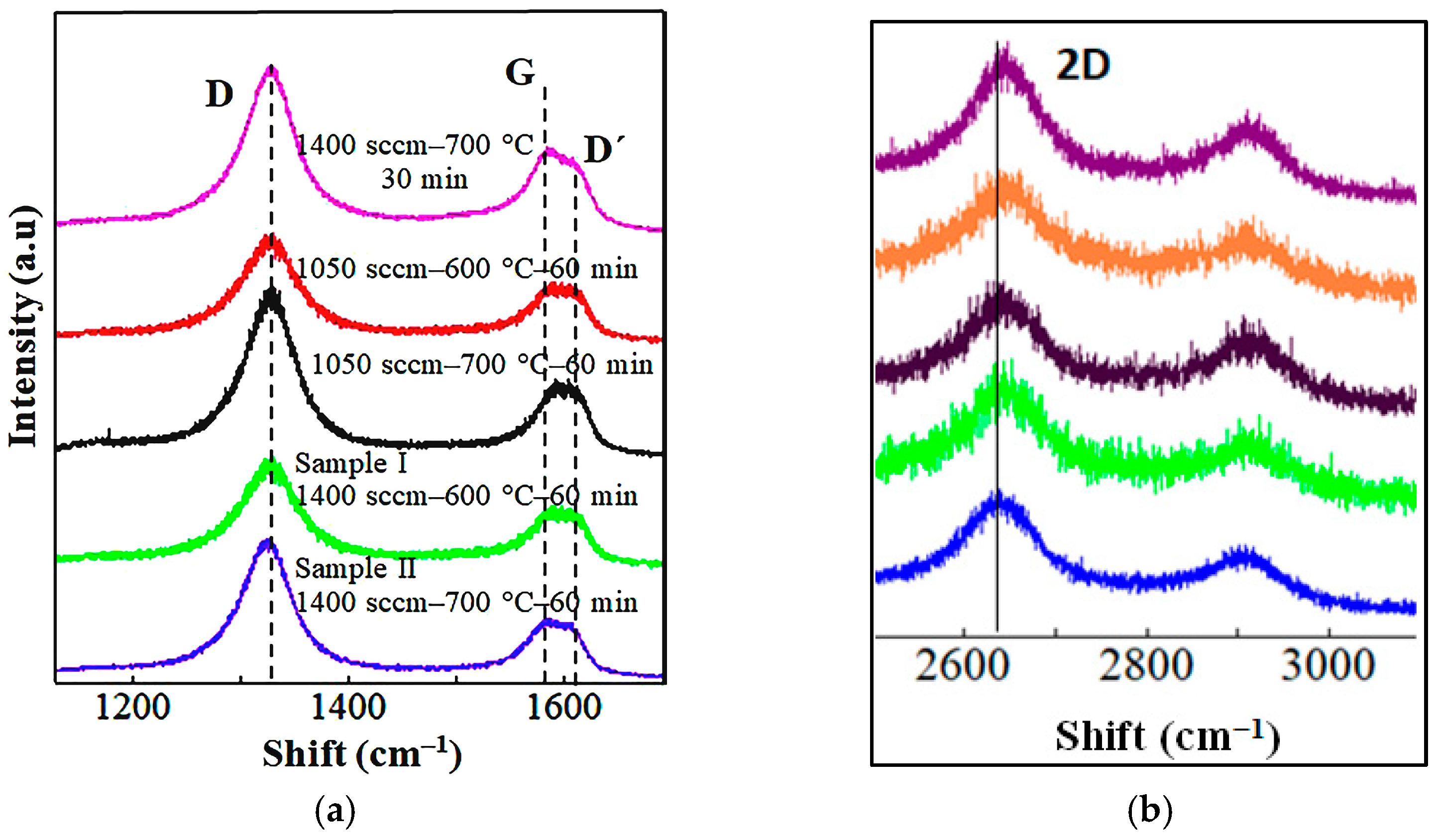
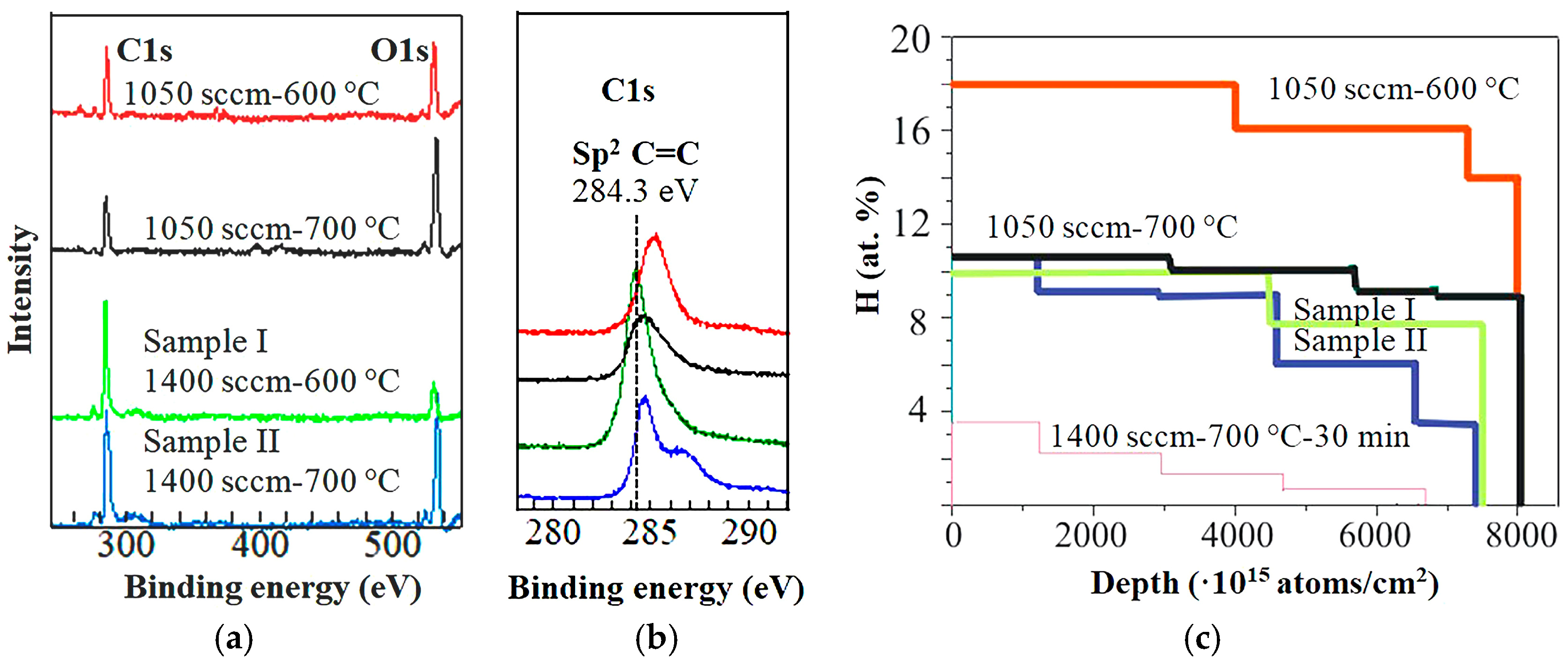
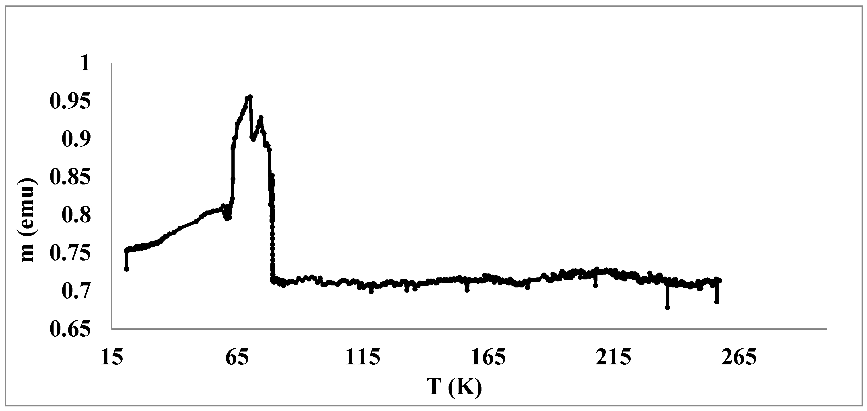
3.1. Morphological and Microstructural Characteristics

Figure 2a–d present the SEM image of the CNWs formed with different parameters of synthesis: Ar flux, time and deposition temperature. In the samples synthetized at 60 min, the thickness of the walls (the longitude in the transverse direction to the substrate obtained by a cross-sectional SEM image) decrease from 3.1 to 1.5 µm, reducing the Ar flux or increasing the temperature, while the lengths of the walls became almost saturated around 1.5 µm. This suggests that, in contrast to the Ar flux, the temperature re-evaporates the nucleation sites, as is necessary for the growing of the walls. The sample formed in less time deposition, 30 min, only grows to around 0.23 µm and 0.5 µm in length and thickness, respectively. Table 1 shows a summary of the values obtained.
The interlayer space of the walls varies between 0.33 and 0.35 nm, as observed in the TEM images (Figure 3a). The increase of the defect amount and temperature may break the single wall structure into many graphene nanocrystallites (GNs) (see Figure 3b,c), since each wall is composed of small graphite regions or nanographite domains [29]. The in-plane lattice constant of the GNs (observed as fringes in Figure 3c) is comparable to that of the graphite (2.53 ± 0.10 Å and 2.46 Å [30], respectively). Additionally, it was found that there were nanoparticles with curved layers (see Figure 3d), similar to those obtained by Gomez-Hernandez from carbon black [31].
The Raman spectra (see Figure 4a,b) reveal a strong G-peak around 1580   c m 1 , which confirms the apparition of the graphene sheets and assigned to E2g phonons from the Brillouin zone [32]. The D-band around 1354   c m 1 is activated with induced disorder. Another peak appears around 1614, named D′, identified on the edges. The relation between the intensities of the peaks I(D)/I(G), associated with disorder, is presented in Table 1. An increase of the values is caused by the deposition temperature due to the size reduction of the clusters by re-evaporation that consequently would create defects. Similarly, the application of short time (30 min) leads to high defects (I(D)/I(G) = 2.4) because the radical formations and nucleation sites are not formed enough. Here, the influence of the Ar flux is weak.
Different types of defects can be defined, such as edges, grain boundaries, vacancies, substitutional and implanted atoms, and a change of carbon hybridization (for example, from sp2 into sp3) [33]. The average defect distance between the point defects ( L D ) can be related to the invers I(D)/I(G), using the following equation [34]:
L D 2 ( n m 2 ) = C D E L 4 I ( G ) I ( D )
where Cd = 3600 and EL is the excitation laser energy used in the Raman experiment (1.96 eV). Table 1 reveals the values obtained. The nature of the defects can be identified by the I(D)/I(D′) relation. According to Eckmann et al. [35], the I(D)/I(D′) around 3.5 is attributed to boundary-like defects in graphite-related materials. As a consequence, the values presented in Table 1 show that the disorder-induced bands would occurs principally from aggregates of crystallite border (one-dimensional defects) [36], which are the most common case of disorder [37]. The crystallite sizes (La) can be related to the invers I(D)/I(G), using the following equation [38]:
L a ( n m ) = C a E L 4 I ( G ) I ( D )
where Ca = 560. Therefore, the increase of the I(D)/I(G) with temperature causes the disassembly of the graphene layers into nanocrystals (Sample I, La = 21.1 nm and Sample II, La = 17.3 nm) with an increase of their population. These values are approximated since many papers have modified the respective equations. For example, Mallet et al. [39] regarded Ca = 4.4 × (2.41)4 and Ribeiro-Soaresa et al. [40] CA = (490 ± 100) × 103. In this sense, the La calculated here approximates to the GNs size observed in TEM images (~9 nm).
Interesting, the 2D band (see Figure 4b) shows a single Lorentzian deconvolution—which is a hallmark of few layers [41], but with a low intensity comparable to graphite [42]. The shift of this band to low frequencies corresponds to a reduction of the graphene-layer numbers [43]. Increasing both the temperature and the Ar flux, the lower value of the 2D position (see Figure 4b and Table 1) appears on Sample II at 2639 c m 1 (blue line). Thus, it behaves more like graphene structure with a few layers [43].
The X-ray photoelectron spectra (Figure 5a,b) and the ERDA measurements (Figure 5c) reveal the relative atomic concentrations of the carbon and oxygen atoms, and the hydrogen content in the CNWs, respectively. The oxygen is binding from moderate vacuum, substrate or atmospheric ambient, which creates more irreversible doping. The relative concentration of oxygen (percent) is reduced as the Ar flux increases or temperature decreases, in association with the defect decline. In addition, this occurs at the expense of the increment of the carbon atoms. Thus, the graphitization is observed on Samples I (green line) and Sample II (blue line). The high carbon concentration around 86.44% on Sample I (see Table 1) is confirmed with the position of the C1s band at 284.3 eV related to the Sp2 C=C binding (see the green line in Figure 5b). Additionally, the ERDA measurements show that the Sample I and Sample II do not incorporate large amounts of hydrogen either. The nanostructure growth for 30 min (purple line) presents a lower amount of hydrogen because of the incipient formation of the graphene layers; however, a posterior study should be performed to evaluate the oxygen content.

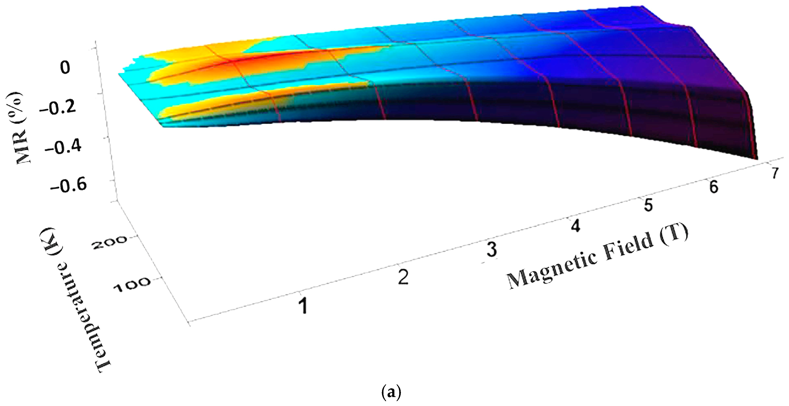
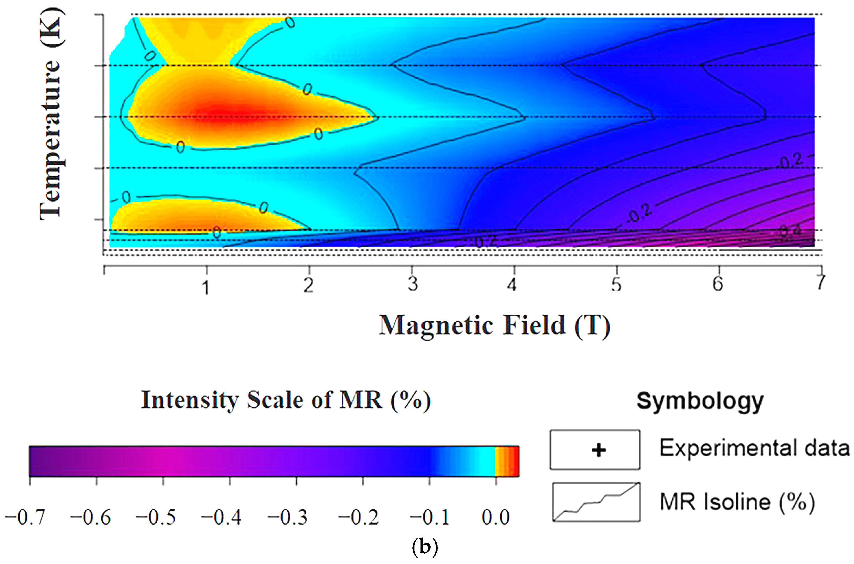
3.2. Magnetoresistance

The Sample I and Sample II were selected for the magnetotransport studies because they present different grades of disorder and, at the same time, have attractive structural and morphological qualities, such as few graphene layers in the walls, large dimensions, high graphitization and a reduced contamination by hydrogen or oxygen atoms. The oxygen bonded in the graphene lattice or on the basal plane produces a charge transfer [44] and the carrier concentration of the CNWs becomes slightly higher [45].

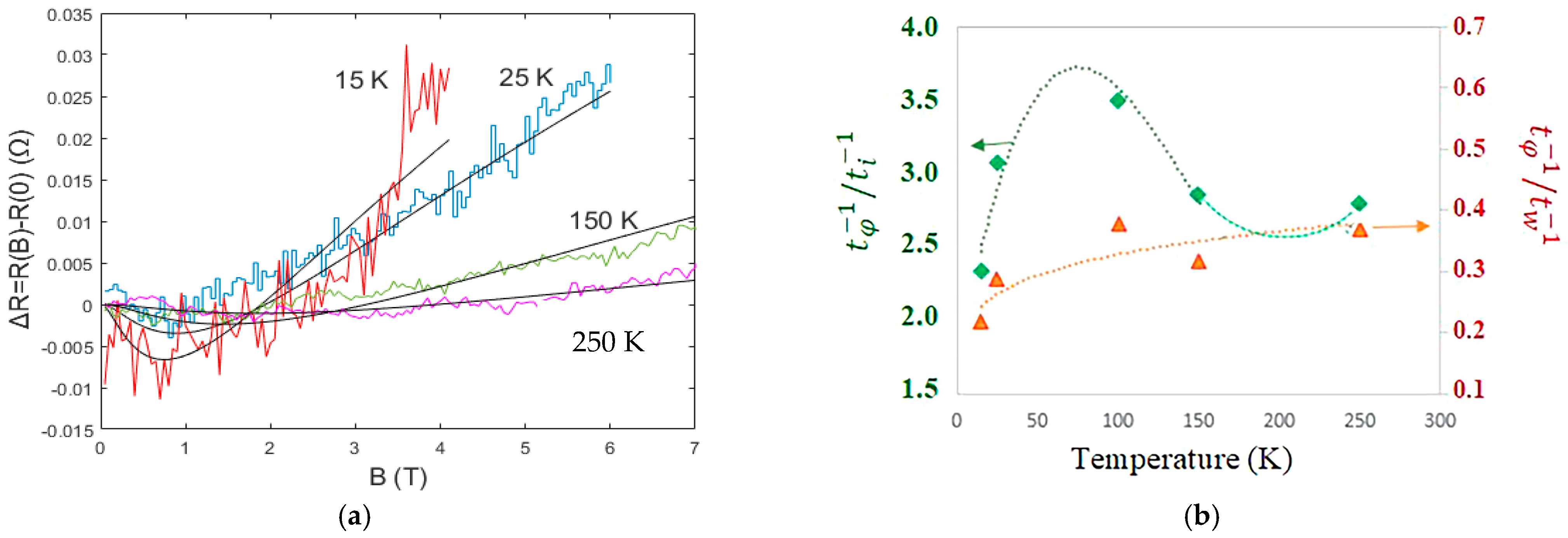
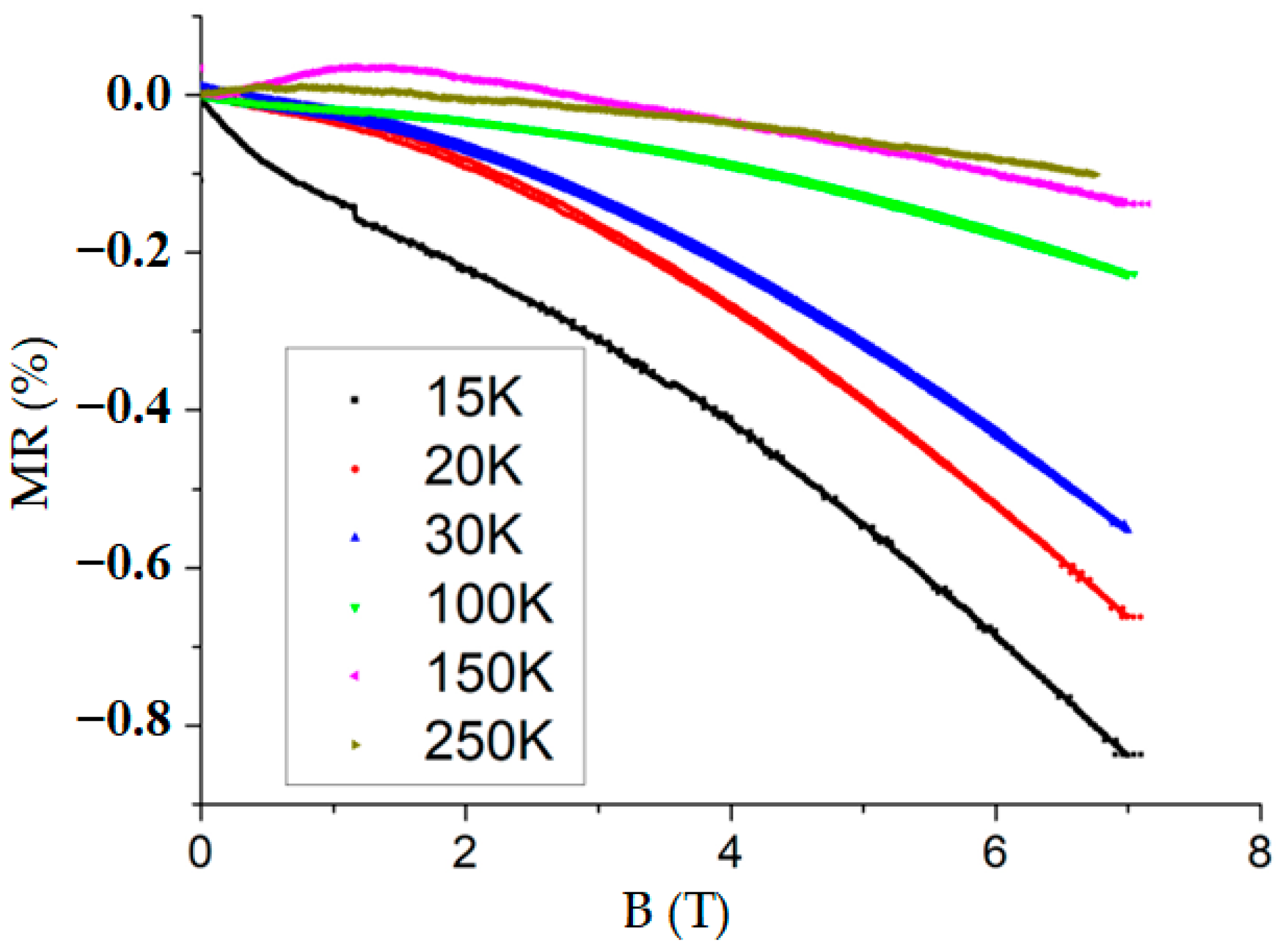
3.2.1. Sample I, Low Disorder

The interference effect between the charges’ carriers is most pronounced in low-dimensional systems (such as graphene) because there are higher probabilities to intersect their own path, leading to the weak localization (WL). The McCann’s model [46] is used to confirm the presence of weak localization and antilocalization. It points out that the phase of interference correction to the magnetoresistance in graphene can be expressed as follows:
R = R 2 e 2 π h F 2 τ φ τ B F 2 τ B τ φ 1 + 2 τ i 1 2 F 2 τ B τ φ 1 + τ i 1 + τ 1
where R = R B R 0 , F z = l n Z + ψ 1 2 + 1 Z and ψ is the Digamma Function. Moreover, τ B = h 2 e D B , τ 1 = τ s 1 + τ w 1 , D is the diffusion coefficient and e de charge of electron. The τ w 1 and τ s 1 are the trigonal warping and elastic scattering rate, respectively. The intervalley scattering τ i 1 is an elastic process wherein a charge is scattered from the edges or defects with the size of the order of the lattice space (adatoms and vacancies) [47], while the phase coherence τ φ 1 is originated via electron-phonon scattering. The quantum correction to the conductivity occurs when τ φ 1 < τ i 1 . The first term in Equation (4) corresponds to WL, while both the second and third terms correspond to WAL.
Figure 6a shows the R as a function of the magnetic field for Sample I. The good fit with the McCann’s model (represented in black lines) confirms the apparition of the WL and WAL effect. The transition from WL to WAL occurs around 0.7 T, at low temperature (below 100 K), with a displacement along the x-axis for higher temperatures (above 100 K). This last one corresponds to the reduction of the τ φ 1 / τ i 1 relation (3.5 to 2.7 for T = 100 K and T = 250 K, respectively); see Figure 6b, the green line. Above 100 K, the τ i 1 increases with more rate than τ φ 1 , probably by an addition of electron-like carriers from interfaces and impurities (interstitials, excess atoms or ions). In Figure 6b (red line), the temperature causes an increment of the number of phonons, which could be released from the substrate, thus improving the phase coherence τ φ 1 .
A general view of the WL-to-WAL transition can be seen in Figure 7a, which represents the 3D magnetoresistance as a function of the magnetic field and temperature. It denotes an evident crossover around 100 K, where, above this temperature, the negative values of MR (blue region) achieve a higher magnetic field.

3.2.2. Sample II, High Disorder

Sample II shows a linear positive MR only below 2 T on approximately all ranges of temperature (40–75 K and 120–250 K) and a negative MR for the higher magnetic field (see Figure 8 and Figure 9a). The MR varies fundamentally with the magnetic field and slightly with the temperature.
The transition from WL to WAL is suppressed for Sample II. The linear positive MR at low field (below 2 T) could be associated with in-plane graphene transport via a hopping mechanism due to the large number of defects. This is in agreement with the results obtained by Kovelevich and coworkers [48] in graphite with disorder and Shlimak and collaborators [49] in irradiated monolayer. The process is based on the spin polarization and the electron–electron interaction [50]. At a low magnetic field, the spin polarization of localized electrons into a single graphene layer dominates rather than magneto-orbital effects. As the magnetic field increases, more localized sites present a spin aligned to the field, and the hops are suppressed through Pauli blockade, leading to a positive MR [51]. This positive MR has no limitation for the observation at high temperatures, which is consistent with our result. Above 2 T, the hops are canceled due to the Pauli blockade, and the transport is dominated by diffusion of electrons associated with the negative and quadratic magnetic field dependence of the MR. The electronic charges could be scattered among graphene nanocrystallites that reduce the carrier mean free path. Zhou and collaborators [52] also reported the effect on the graphene monolayer. The negative diffusion magnetoresistance, M R D s , is given by the following:
M R D s = l l 0 = K B 2
where l is the increment of the mean free path of the charge carriers caused by the magnetic field, l 0 is the mean free path of the carrier without magnetic field and K is a constant [5]. The lengthening of the mean free path with greater magnetic field leads to a negative M R D s .

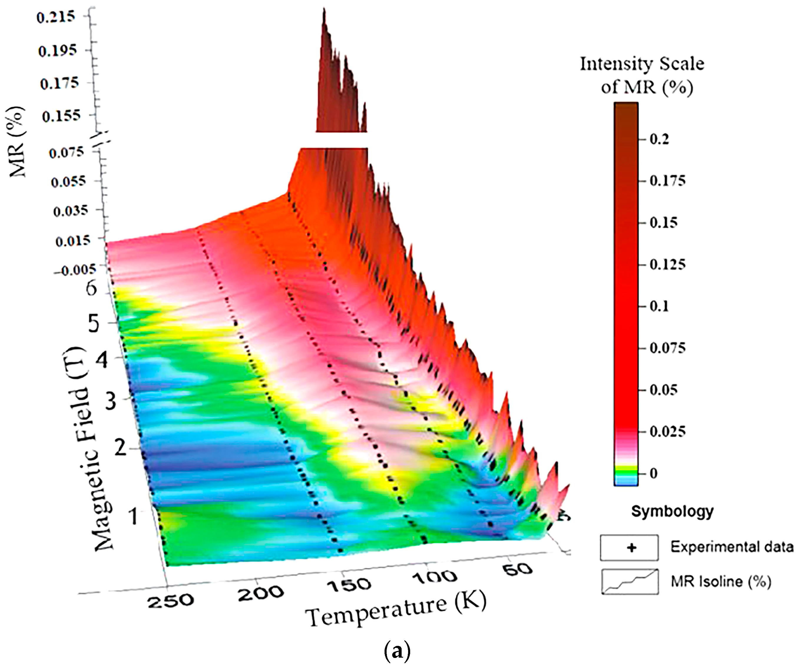
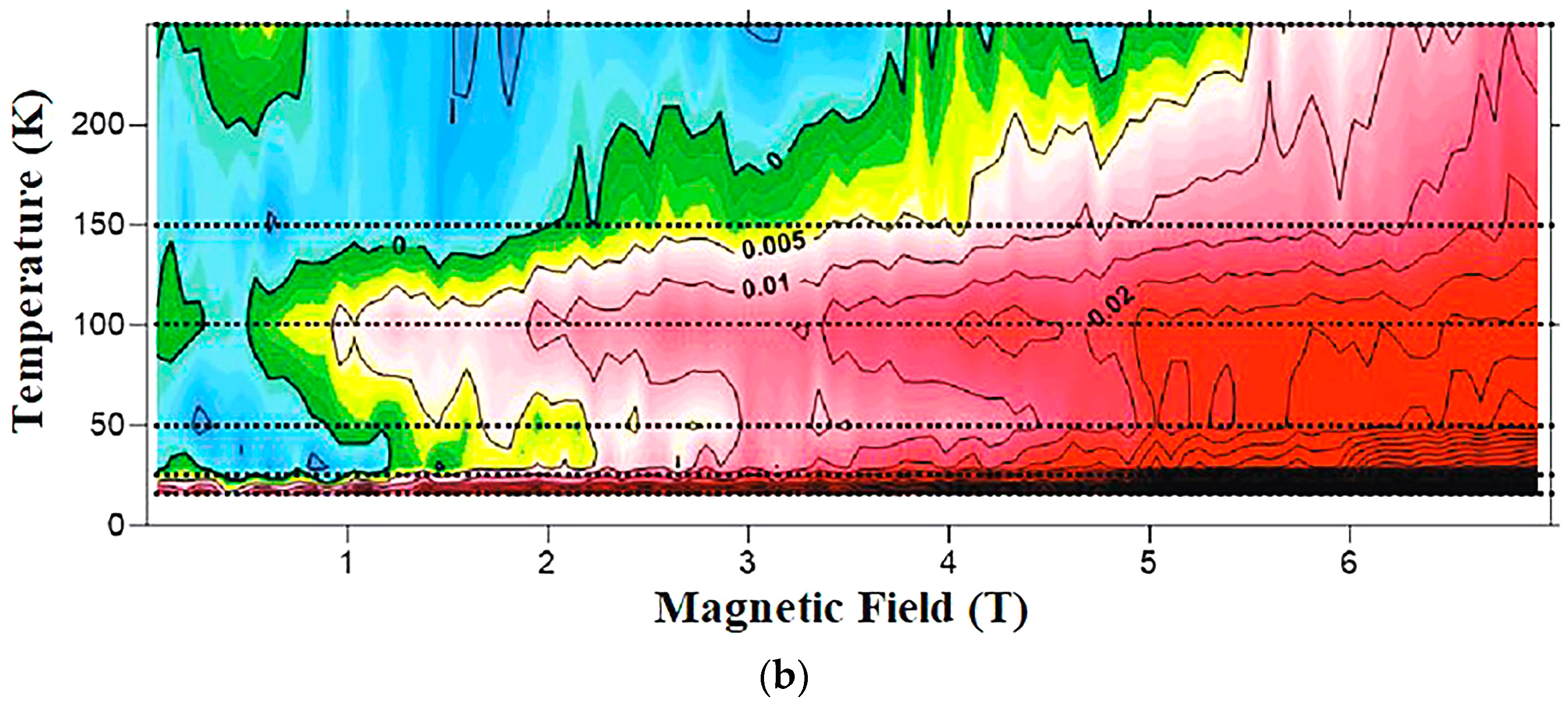
3.2.3. MR Isoline Maps

The MR isoline maps for both samples (Figure 7b and Figure 9b) show below 50 K an increase of the isoline density related to an increase of the MR variation. This effect is characteristic of the network structure and independent of the number of defects. For making a clear interpretation, we carried out measurements of the magnetic moment depending on the temperature, m(T) (see Figure 10). A maxim value of the magnetization curve is observed around 65K, indicating the presence of magnetic entities. Davami and collaborators [21] also reported such behavior at T = 50 K as a result of magnetic phase transitions. Fernandez-Rossier and collaborators [53] reported a coexistence between antiferromagnetic and ferromagnetic order for graphene. Different origins may cause the magnetic entities, such as the presence of carbon nanoparticles [54], the ion bombardment [55] over the sample during the deposition, defects such as domains and interfaces, and chemisorption of hydrogen and oxygen [56,57].
The maximum of the magnetization occurs approximately in the time with the variation the MR isoline density at 50 K. During the sweeping of the magnetic field to 7 T in the MT measurements, the electrons are spin-polarized with the field, and the scattering effect would be spin dependent, which should cause the variation of the MR isoline density.

4. Conclusions

The variation of the deposition temperature strongly modified the disorder and graphitization of the CNWs, and this, in turn, modified the magnetotransport properties. Sample I revealed a negative MR caused by weak localization in the presence of defects and a transition to the WAL effect, as is characteristic to the in-plane graphene transport. However, the highly disordered structure, Sample II, led to the Hopping mechanism and a diffusion transport from extrinsic electron scattering on graphene nanocrystallites. At a low temperature (15 K), Sample I enhanced a maxim M R at 0.2%, while Sample II at 0.8%. The MR isoline maps for both samples show, below 50 K, an increase of the isoline density associated with the presence of magnetic entities. The microstructural tunability of the CNWs obtained introduces new perspectives for magneto-electronic devices.

Author Contributions

Formal analysis, investigation, software, writing—original draft, review and editing preparation, M.A.G.; methodology, S.V., M.V., R.G.G. and S.A.; conceptualization, R.G.G., M.A.G. and R.A.R.-C.; Validation, S.V., M.V., S.A., J.J.A.P., R.A.R.-C. and G.D.; Resources, project administration, funding acquisition, R.A.R.-C., J.M.P., J.J.A.P., M.V., G.D. and M.A.G.; Data curation, M.A.G., S.V., S.A. and J.J.A.P. All authors have read and agreed to the published version of the manuscript.

Funding

This work was financial supported for J.M.P. through CONACYT Programme, Mexico; M.A.G. and J.J.A.P. by the postdoctoral programme from the Meritorious Autonomous University of Puebla (BUAP), Mexico; G.D. from the National Institute for Lasers, Plasma and Radiation Physics (INFLPR), Romania, and R.A.R.-C. from University of Guanajuato, Mexico. M.V. acknowledges the financial support of a grant of the Ministry of Research, Innovation and Digitization, CCCDI—UEFISCDI, project number PN-III-P2-2.1-PED-2021-3112, 597PED/2022, within PNCDI III.

Institutional Review Board Statement

Not applicable.

Informed Consent Statement

Not applicable.

Data Availability Statement

Not applicable.

Acknowledgments

We want to thank Ion Burducea for ERDA research and Roberto Mora Monroy for XPS measurements.

Conflicts of Interest

The authors declare no conflict of interest. The funders had no role in the design of the study; in the collection, analyses, or interpretation of data; in the writing of the manuscript; or in the decision to publish the results.

References

  1. Tikhonenko, F.V.; Horsell, D.W.; Gorbachev, R.V.; Savchenko, A.K. Weak localization in graphene flakes. Phys. Rev. Lett. 2008, 100, 056802–056805. [Google Scholar] [CrossRef]
  2. Liu, Y.; Lew, W.S.; Sun, L. Enhanced weak localization effect in few-layer graphene. Phys. Chem. Chem. Phys. 2011, 13, 20208–20214. [Google Scholar] [CrossRef] [PubMed]
  3. Kechedzhi, K.; Fal’ko, V.I.; McCann, E.; Altshuler, B.L. Influence of trigonal warping on interference effects in bilayer graphene. Phys. Rev. Lett. 2007, 98, 176806–176809. [Google Scholar] [CrossRef]
  4. Ki, D.K.; Jeong, D.; Choi, J.H.; Lee, H.J. Inelastic scattering in a monolayer graphene sheet; a weak-localization study. Phys. Rev. B 2008, 78, 125409–125413. [Google Scholar] [CrossRef]
  5. Zhang, X.; Xue, Q.; Zhu, D. Positive and negative linear magnetoresistance of graphite. Phys. Lett. A 2004, 320, 471–477. [Google Scholar] [CrossRef]
  6. Morpurgo, A.F.; Guinea, F. Intervalley scattering, long-range disorder, and effective time-reversal symmetry breaking in graphene. Phys. Rev. Lett. 2006, 97, 196804–196807. [Google Scholar] [CrossRef] [PubMed]
  7. Lara-Avila, S.; Tzalenchuk, A.; Kubatkin, S.; Yakimova, R.; Janssen, T.; Cedergren, K.; Bergsten, T.; Falko, V. Disordered Fermi Liquid in Epitaxial Graphene from Quantum Transport Measurements. Phys. Rev. Lett. 2011, 107, 166602–166606. [Google Scholar] [CrossRef] [PubMed]
  8. Esquinazi, P.; Krüger, J.; Barzola-Quiquia, J.; Schönemann, R.; Herrmannsdörfer, T.; García, N. On the low-field Hall coefficient of graphite. AIP Adv. 2014, 4, 117121. [Google Scholar] [CrossRef]
  9. Li, J.; Liu, Z.; Guo, Q.; Yang, S.; Xu, A.; Wang, Z.; Wang, G.; Wang, Y.; Chen, D.; Ding, G. Controllable growth of vertically oriented graphene for high sensitivity gas detection. J. Mater. Chem. C 2019, 7, 5995–6003. [Google Scholar] [CrossRef]
  10. Zhai, Z.; Leng, B.; Yang, N.; Yang, B.; Liu, L.; Huang, N.; Jiang, X. Rational Construction of 3D-Networked Carbon Nanowalls/Diamond Supporting CuO Architecture for High-Performance Electrochemical Biosensors. Small 2019, 15, 1901527. [Google Scholar] [CrossRef] [PubMed]
  11. Dinh, T.; Achour, A.; Vizireanu, S.; Dinescu, G.; Nistor, L.; Armstrong, A.; Guay, D.; Pech, D. Hydrous RuO2/carbon nanowalls hierarchical structures for all-solid-state ultrahigh-energy-density micro-supercapacitors. Nano Energy 2014, 10, 288–294. [Google Scholar] [CrossRef]
  12. Hung, T.-C.; Chen, C.-F.; Whang, W.-T. Deposition of carbon nanowall flowers on two-dimensional sheet for electrochemical capacitor application. Electrochem. Solid-State Lett. 2009, 12, 6. [Google Scholar] [CrossRef]
  13. Yue, Z.; Levchenko, I.; Kumar, S.; Seo, D.; Wang, X.; Doua, S.; Ostrikov, K. Large networks of vertical multi-layer graphenes with morphology-tunable magnetoresistance. Nanoscale 2013, 5, 9283–9288. [Google Scholar] [CrossRef]
  14. Huang, J.; Guo, L.-W.; Li, Z.-L.; Chen, L.-L.; Lin, J.-J.; Jia, Y.-P.; Lu, W.; Guo, Y.; Chen, X.-L. Anisotropic quantum transport in a network of vertically aligned graphene sheets. J. Phys. Condens. Matter 2014, 26, 345301. [Google Scholar] [CrossRef]
  15. Hiramatsu, M.; Nihashi, Y.; Kondo, H.; Hori, M. Nucleation Control of Carbon Nanowalls Using Inductively Coupled Plasma-Enhanced Chemical Vapor Deposition. Jpn. J. Appl. Phys. 2013, 52, 01AK05. [Google Scholar] [CrossRef]
  16. Lin, J.; Guo, L.; Huang, Q.; Jia, Y.; Li, K.; Lai, X.; Chen, X. Anharmonic phonon effects in Raman spectra of unsupported vertical graphene sheets. Phys. Rev. B 2011, 83, 125430. [Google Scholar] [CrossRef]
  17. Zhang, H.; Kikuchi, N.; Kogure, T.; Kusano, E. Growth of carbon with vertically aligned nanoscale flake structure in capacitively coupled rf glow discharge. Vacuum 2008, 82, 754–759. [Google Scholar] [CrossRef]
  18. Shang, N.G.; Au, F.C.K.; Meng, X.M.; Lee, C.S.; Bello, I.; Lee, S.T. Uniform carbon nanoflake films and their field emissions. Chem. Phys. Lett. 2002, 358, 187–191. [Google Scholar] [CrossRef]
  19. Tanaka, K.; Yoshimura, M.; Okamoto, A.; Ueda, K. Growth of carbon nanowalls on a SiO2 substrate by microwave plasma-enhanced chemical vapor deposition. Jpn. J. Appl. Phys. 2005, 44, 2074–2076. [Google Scholar] [CrossRef]
  20. Vesel, A.; Zaplotnik, R.; Primc, G.; Mozetič, M. Synthesis of Vertically Oriented Graphene Sheets or Carbon Nanowalls—Review and Challenges. Materials 2019, 12, 2968. [Google Scholar] [CrossRef] [Green Version]
  21. Davami, K.; Shaygan, M.; Kheirabi, N.; Zhao, J.; Kovalenko, D.A.; Rummeli, M.H.; Opitz, J.; Cuniberti, G.; Lee, J.-S.; Meyyappan, M. Synthesis and characterization of carbon nanowalls on different substrates by radio frequency plasma enhanced chemical vapor deposition. Carbon 2014, 72, 372. [Google Scholar] [CrossRef]
  22. Vizireanu, S.; Mitu, B.; Luculescu, C.; Nistor, L.; Dinescu, G. PECVD synthesis of 2D nanostructured carbon material. Surf. Coat. Technol 2012, 211, 2–8. [Google Scholar] [CrossRef]
  23. Zhang, H.; Wu, S.; Lu, Z.; Chen, X.; Chen, Q.; Gao, P.; Yu, T.; Peng, Z.; Ye, J. Efficient and controllable growth of vertically oriented graphene nanosheets by mesoplasma chemical vapor deposition. Carbon 2019, 147, 341–347. [Google Scholar] [CrossRef]
  24. Lenz, J.E. A review of magnetic sensors. Proc. IEEE 1990, 78, 973. [Google Scholar] [CrossRef]
  25. Daughton, J.M. GMR applications. J. Magn. Magn. Mater. 1999, 192, 334. [Google Scholar] [CrossRef]
  26. Acosta Gentoiu, M.; Betancourt-Riera, R.; Vizireanu, S.; Burducea, I.; Marascu, V.; Stoica, S.D.; Bita, B.I.; Dinescu, G.; Riera, R. Morphology, Microstructure and Hydrogen content of Carbon Nanostructures Obtained by PECVD at Various Temperatures. J. Nanomater. 2017, 2017, 1374973. [Google Scholar] [CrossRef]
  27. Vizireanu, S.; Ionita, M.D.; Ionita, R.E.; Stoica, S.D.; Teodorescu, C.M.; Husanu, M.A.; Apostol, N.G.; Baibarac, M.; Panaitescu, D.; Dinescu, G. Aging phenomena and wettability control of plasma deposited carbon nanowall layers. Plasma Process. Polym. 2017, 14, 1700023. [Google Scholar] [CrossRef]
  28. Vizireanu, S.; Ionita, M.D.; Dinescu, G.; Enculescu, I.; Baibarac, M.; Baltog, I. Post-synthesis carbon nanowalls transformation under hydrogen, oxygen, nitrogen, tetrafluoroethane and sulfur hexafluoride plasma treatments. Plasma Process. Polym. 2012, 9, 363–370. [Google Scholar] [CrossRef]
  29. Kobayashi, K.; Tanimura, M.; Nakai, H.; Yoshimura, A.; Yoshimura, H.; Kojima, K.; Tachibana, M. Nanographite domains in carbon nanowalls. J. Appl. Phys. 2007, 101, 94306. [Google Scholar] [CrossRef]
  30. Baskin, Y.; Meyer, L. Lattice Constants of Graphite at Low Temperatures. Phys. Rev. 1955, 100, 544. [Google Scholar] [CrossRef]
  31. Gomez-Hernandez, R.; Panecatl-Bernal, Y.; Mendez-Rojas, M.A. High yield and simple one-step production of carbon black nanoparticles from waste tires. Heliyon 2019, 5, e02139. [Google Scholar] [CrossRef]
  32. Tuinstra, F.; Koenig, J.L. Raman Spectrum of Graphite. J. Chem. Phys. 1970, 53, 1126. [Google Scholar] [CrossRef]
  33. Eckmann, A.; Felten, A.; Verzhbitskiy, I.; Davey, R.; Casiraghi, C. Raman study on defective graphene: Effect of the excitation energy, type, and amount of defects. Phys. Rev. B 2013, 88, 035426–035436. [Google Scholar] [CrossRef]
  34. Sozaraj, S.R.; Caridad, J.M.; Schulte, L.; Cagliani, A.; Borah, D.; Morris, M.A.; Bøggild, P.; Ndoni, S. High quality sub-10 nm graphene nanoribbons by on-chip PS-b-PDMS block copolymer lithography. RSC Adv. 2015, 5, 66711. [Google Scholar]
  35. Eckmann, A.; Felten, A.; Mishchenko, A.; Britnell, L.; Krupke, R.; Novoselov, K.S.; Casiraghi, C. Probing the Nature of Defects in Graphene by Raman Spectroscopy. Nano Lett. 2012, 12, 925–3930. [Google Scholar] [CrossRef]
  36. Cançado, L.G.; Jorio, A.; Ferreira, E.H.M.; Stavale, F.; Achete, C.; Capaz, R.B.; Moutinho, M.V.O.; Lombardo, A.; Kulmala, T.S.; Ferrari, A.C. Quantifying Defects in Graphene via Raman Spectroscopy at Different Excitation Energies. Nano Lett. 2011, 11, 3190–3196. [Google Scholar] [CrossRef]
  37. Pimenta, M.A.; Dresselhaus, G.; Dresselhaus, M.S.; Cancado, L.G.; Jorio, A.; Saito, R. Studying disorder in graphite-based systems by Raman spectroscopy. Phys. Chem. Chem. Phys. 2007, 9, 1276–1291. [Google Scholar] [CrossRef]
  38. Cançado, L.G.; Takai, K.; Enoki, T.; Endo, M.; Kim, Y.A.; Mizusaki, H.; Jorio, A.; Coelho, L.N.; Magalhães-Paniago, R.; Pimenta, M.A. General equation for the determination of the crystallite size La of nanographite by Raman spectroscopy. Appl. Phys. Lett. 2006, 88, 163106. [Google Scholar] [CrossRef]
  39. Mallet-Ladeira, P.; Puech, P.; Toulouse, C.; Cazayous, M.; Ratel-Ramond, N.; Weisbecker, P.; Vignoles, G.L.; Monthioux, M. A Raman study to obtain crystallite size f carbon materials: A better alternative to the Tuinstra–Koenig law. Carbon 2014, 80, 629–639. [Google Scholar] [CrossRef]
  40. Ribeiro-Soaresa, J.; Oliverosc, M.E.; Garinc, C.; Davidc, M.V.; Martinsa, L.G.P.; Almeidac, C.A.; Martins-Ferreirac, E.H.; Takai, K.; Enoki, T.; Magalhães-Paniago, R.; et al. Structural analysis of polycrystalline graphene systems by Raman spectroscopy. Carbon 2015, 95, 646–652. [Google Scholar] [CrossRef]
  41. Reina, A.; Jia, X.; Ho, J.; Nezich, D.; Son, H.; Bulovic, V.; Dresselhaus, M.S.; Kong, J. Large area, few-layer graphene films on arbitrary substrates by chemical vapor deposition. Nano Lett. 2008, 9, 30–35. [Google Scholar] [CrossRef]
  42. Ferrari, A.C.; Meyer, J.C.; Scardaci, V.; Casiraghi, C.; Lazzeri, M.; Mauri, F.; Piscanec, S.; Jiang, D.; Novoselov, S.; Roth, S.; et al. Raman Spectrum of Graphene and Graphene Layers. Phys. Rev. Lett. 2006, 97, 187401. [Google Scholar] [CrossRef] [PubMed]
  43. Ni, Z.; Wang, Y.; Yu, T.; Shen, Z. Raman spectroscopy and imaging of graphene. Nano Res. 2008, 1, 273–291. [Google Scholar] [CrossRef]
  44. Mackenzie, D.; Galbiati, M.; Cerio, X.; Sahalianov, I.; Radchenko, T.; Sun, J.; Peña, D.; Gammelgaard, L.; Jessen, B.; Thomsen, J.; et al. Unraveling the electronic properties of graphene with substitutional oxygen. 2D Mater. 2021, 8, 045035. [Google Scholar] [CrossRef]
  45. Takeuchi, W.; Takeda, K.; Hiramatsu, M.; Tokuda, Y.; Kano, H.; Kimura, S.; Sakata, O.; Tajiri, H.; Hori, M. Monolithic self-sustaining nanographene sheet grown using plasma-enhanced chemical vapor deposition. Phys. Status Solidi (A) 2010, 207, 139–143. [Google Scholar] [CrossRef]
  46. McCann, E.; Kechedzhi, K.; Fal’ko, V.I.; Suzuura, H.; Ando, T.; Altshuler, B.L. Weak localisation magnetoresistance and valley symmetry in graphene. Phys. Rev. Lett. 2006, 97, 146805–146808. [Google Scholar] [CrossRef] [PubMed]
  47. Pezzini, S.; Cobaleda, C.; Diez, E.; Bellani, V. Disorder and de-coherence in graphene probed by low-temperature magneto-transport:weak localization and weak antilocalization. J. Phys. Conf. Ser. 2013, 456, 012032. [Google Scholar] [CrossRef]
  48. Kopelevich, Y.; da Silva, R.R.; Camargo, B.C.; Alexandrov, A.S. Extraordinary magnetoresistance in graphite: Experimental evidence for the time-reversal symmetry breaking. J. Phys. Condens. Matter 2013, 25, 466004. [Google Scholar] [CrossRef] [PubMed]
  49. Shlimak, I.; Zion, E.; Butenko, A.; Wolfson, L.; Richter, V.; Kaganovskii, Y.; Sharoni, A.; Haran, A.; Naveh, D.; Kogan, E.; et al. Hopping magnetoresistance in ion irradiated monolayer graphene. Phys. E Low-Dimens. Syst. Nanostruct. 2016, 76, 158–163. [Google Scholar] [CrossRef]
  50. Kamimura, H.; Kurobe, A.; Takemori, T. Magnetoresistance in Anderson-localized systems. Physica B+C 1983, 117–118, 652. [Google Scholar] [CrossRef]
  51. Zhao, H.L.; Spivak, B.Z.; Gelfand, M.P.; Feng, S. Negative magnetoresistance in variable-range-hopping conduction. Phys. Rev. B 1991, 44, 10760–10767. [Google Scholar] [CrossRef] [PubMed]
  52. Zhou, Y.B.; Han, B.H.; Liao, Z.M.; Wu, H.C.; Yu, D.P. From positive to negative magnetoresistance in graphene with increasing disorder. Appl. Phys. Lett. 2011, 98, 222502. [Google Scholar] [CrossRef]
  53. Fernandez-Rossier, J.; Palacios, J.J. Magnetism in graphene nanoislands. Phys. Rev. Lett. 2007, 99, 177204. [Google Scholar] [CrossRef] [PubMed]
  54. Parkanskya, N.; Alterkopa, B.; Boxmana, R.L.; Leitusb, G.; Berkhc, O.; Barkayd, Z.; Rosenberg, Y.; Eliaz, N. Magnetic properties of carbon nano-particles produced by a pulsed arc submerged in ethanol. Carbon 2008, 46, 215–219. [Google Scholar] [CrossRef]
  55. Esquinazi, P.; Spemann, D.; Höhne, R.; Setzer, A.; Han, K.-H.; Butz, T. Induced magnetic ordering by proton irradiation in graphite. Phys. Rev. Lett. 2003, 91, 227201. [Google Scholar] [CrossRef] [PubMed]
  56. Kusakabe, K.; Maruyama, M. Magnetic nanographite. Phys. Rev. B 2003, 67, 092406. [Google Scholar] [CrossRef]
  57. Yazyev, O.V. Magnetism in disordered graphene and irradiated graphite. Phys. Rev. Lett. 2008, 101, 037203. [Google Scholar] [CrossRef] [PubMed] [Green Version]
Figure 1. CNWs deposited onto electrode configurations for MR measurements.
Applsci 13 02476 g001
Figure 2. The SEM images for the CNWs grown at (a) 1400 sccm-700 °C-30 min, (b) 1050 sccm-600 °C-60 min, (c) 1400 sccm-600 °C-60 min and (d) 1400 sccm-700 °C-60 min.
Applsci 13 02476 g002
Figure 3. TEM images. (a) Interlayer spaces of the walls. (b,c) Graphene nanocrystallites inside the CNWs sample with a diameter around 9 nm. (b) In-plane lattice fringes. (d) Nanoparticles with curved layers inside the CNWs sample.
Applsci 13 02476 g003
Figure 4. The RAMAN spectra for the CNWs grown at 30 min with 1400 sccm-700 °C (purple line) and at 60 min with 1050 sccm-600 °C (red line), 1050 sccm-700 °C (black line), 1400 sccm-600 °C (green line) and 1400 sccm-700 °C (blue line). The figure includes (a) the D and G bands and (b) 2D bands.
Applsci 13 02476 g004
Figure 5. (a,b) The XPS spectra and (c) the ERDA measurements for the CNWs grown at 1050 sccm-600 °C-60 min (red line), 1050 sccm-700 °C-60 min (black line), 1400 sccm-600 °C-60 min (green line) and 1400 sccm-700 °C-60 min (blue line). The figure includes in (a) the C1s and O1s bands, (b) the amplification of the C1s band and (c) the hydrogen content along the transversal section (depth) of the samples, including 1400 sccm-700 °C-30 min (purple line).
Applsci 13 02476 g005
Figure 6. (a) The best fit on Sample I by the model of McCann (black line) with the experimental curves of R = R B R 0 as a function of the magnetic field at different temperatures. (b) The τ φ 1 / τ i 1 and τ φ 1 / τ w 1 rates obtained through the best fit with the τ w 1 fixed.
Applsci 13 02476 g006
Figure 7. (a) Three-dimensional image of the MR in function of the temperature and the magnetic field of Sample I. (b) Isoline map of the MR.
Applsci 13 02476 g007aApplsci 13 02476 g007b
Figure 8. The MR measurement of Sample II.
Applsci 13 02476 g008
Figure 9. (a) Three-dimensional image of the MR in function of the temperature and the magnetic field of Sample II. (b) Isoline map of the MR.
Applsci 13 02476 g009aApplsci 13 02476 g009b
Figure 10. Magnetic moment as a function of the temperature of Sample I.
Applsci 13 02476 g010
Table 1. Values obtained from SEM, TEM, ERDA and Raman spectra of the CNWs formed at different synthesis parameters: time, deposition temperature and Ar flux.
Synthesis ParametersTime (min)3060
Temperature (°C)700600700
Ar Flux (sccm)14001050Sample I 14001050Sample II 1400
Morphology and MicrostructureLength (µm) ±0.30.231.051.5-1.3
Thickness (µm)0.501.503.05-1.52
I(D)/I(G)2.401.811.802.212.20
I(D)/I(D′)4.85.53.24.45.5
La (nm)20.421.021.117.217.3
LD (nm)11.511.711.810.610.6
2D Position (cm−1)26462651264626492639
Carbon Concentration (%) by XPS-64.6486.4455.5074.93
Oxygen Concentration (%) by XPS-35.3613.5644.5025.07
Hydrogen Content by ERDA1.416.79.110.17.8
Disclaimer/Publisher’s Note: The statements, opinions and data contained in all publications are solely those of the individual author(s) and contributor(s) and not of MDPI and/or the editor(s). MDPI and/or the editor(s) disclaim responsibility for any injury to people or property resulting from any ideas, methods, instructions or products referred to in the content.

