Article

Output Properties of Transparent Submount Packaged FlipChip Light-Emitting Diode Modules

1
Department of Electronic Engineering, Chang Gung University, Kweishan, Taoyuan 333, Taiwan
2
Department of Urology, Chang Gung Memorial Hospital, Kweishan, Taoyuan 333, Taiwan
3
Department of Mechanical Engineering, Ming Chi University of Technology, 84 Gungjuan Rd., Taishan Dist., New Taipei City 24301, Taiwan
4
Department of Materials Engineering, Ming Chi University of Technology, Taishan, New Taipei City 243, Taiwan
5
Department of Nephrology, Chang Gung Memorial Hospital, Kweishan, Taoyuan 333, Taiwan
6
Department of Otolaryngology, Head and Neck Surgery, Chang Gung Memorial Hospital, Kweishan, Taoyuan 333, Taiwan
*
Author to whom correspondence should be addressed.
Submission received: 25 May 2016 / Revised: 7 June 2016 / Accepted: 14 June 2016 / Published: 20 June 2016

Abstract

:
Flip chip technology has been widely adopted in modern power light-emitting diode (LED) fabrications and its output efficiency is closely related to the submount material properties. Here, we present the electrical, optical and thermal properties of flip chip light-emitting diodes mounted on transparent sapphire and borosilicate glass which have shown a higher output luminous flux when compared to the traditional non-transparent mounted LEDs. Exhibiting both better thermal conductivity and good optical transparency, flip chip LEDs with a sapphire submount showed superior performance when compared to the non-transparent silicon submount ones, and also showed better optical performance than the flip chip LEDs mounted on transparent but poor-thermal-conducting glass substrates. The correspondent analysis was carried out using ANSYS 14 to compare the experimental thermal imaging with the simulation results. TracePro software was also used to check the output luminous flux dependency on different LED mounting designs.

Graphical Abstract

1. Introduction

The LED efficiency and manufacturing cost are the key issues to affect the commercialization share of solid-state lighting. There are a lot of methods to enhance the LED’s luminous efficiencies, such as improving the LED’s epitaxial quality, modifying the LED’s epitaxial structure [1], increasing the surface roughness of LEDs [2,3,4,5], and improving the heat dissipation, etc. Recently, due to the high power operation of indoor and outdoor lighting, flip chip (FC) technology has been widely used; it can solve the heat accumulation problem effectively. Intense research is being carried out by different groups to improve the light output efficiency of FCLEDs [6,7,8,9,10]. However, most of the FCLED submounts used today are not transparent, which decreases the output light extraction. Besides using highly refractive submounts, an alternative method to increase the FCLED efficiency through lowering the submount absorption is proposed here by using high transparency mounting materials.
In fact, it seems that there is a trade-off between the transparency and the thermal conductivity of the submount materials. Materials such as aluminum and copper have very high thermal conductivity, but they are not transparent [11]. On the other hand, a material such as glass is transparent but its thermal conductivity is very poor when compared to metallic aluminum or copper. It is known that heat dissipation has always been an issue in LED technology. So far, only 18% of the external quantum efficiency is achieved by LEDs [12], with the rest of the power or energy still dissipating out from LEDs as heat. Many groups have proposed different kind of heat-sinking methods with different materials [13,14], but there is still a lack of research on the transparent materials. Although Pan et al. also proposed the architecture of a LED combined with a zinc oxide (ZnO) transparent submount [15], the price of ZnO substrates is expensive, and the LED’s operation currents are only up to 80 mA. Therefore, we have to investigate further to make some practical applications in this area.
In general, to enhance the light extraction implies not only to increase the light output but also to decrease the heat generation. One prospect in the field of improving the light extraction of LEDs is called “bi-directional LEDs”, where light can be collected in both directions through transparent substrates. Furthermore, FCLEDs with transparent submounts can also be used to emit different mixing colors in opposite directions easily. The proposed model for bi-directional LEDs is demonstrated in the inset of Figure 1. By having a transparent substrate, LEDs can emit light in all directions, just like the traditional tungsten light bulb. Unfortunately, as mentioned above, most transparent substrates are not good thermal conductors, and the accumulated heat will severely affect the output performance of LEDs. Most LED manufacturers today prefer to use a silver mirror between the LED dice and the non-transparent metal submount to reflect the light back [16,17]. So, if the metal submount can be replaced by transparent substrates, which can also dissipate heat well. For example, by using sapphire or graphene deposited on glass, an efficient bi-directional LED can be achieved in a cost-effective manner, also with the benefit of a wide light output angle.
Silicon has high stability, low cost and is readily available in large wafer sizes. However, it is very challenging to grow high quality GaN-based LEDs directly on Si due to the large mismatch in lattice constants and the thermal expansion coefficients between GaN and Si [18,19,20,21,22,23,24,25]. Despite all these disadvantages of silicon, in this work we use it as a traditional non-transparent reference submount material due to its easy processing characteristics.

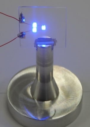
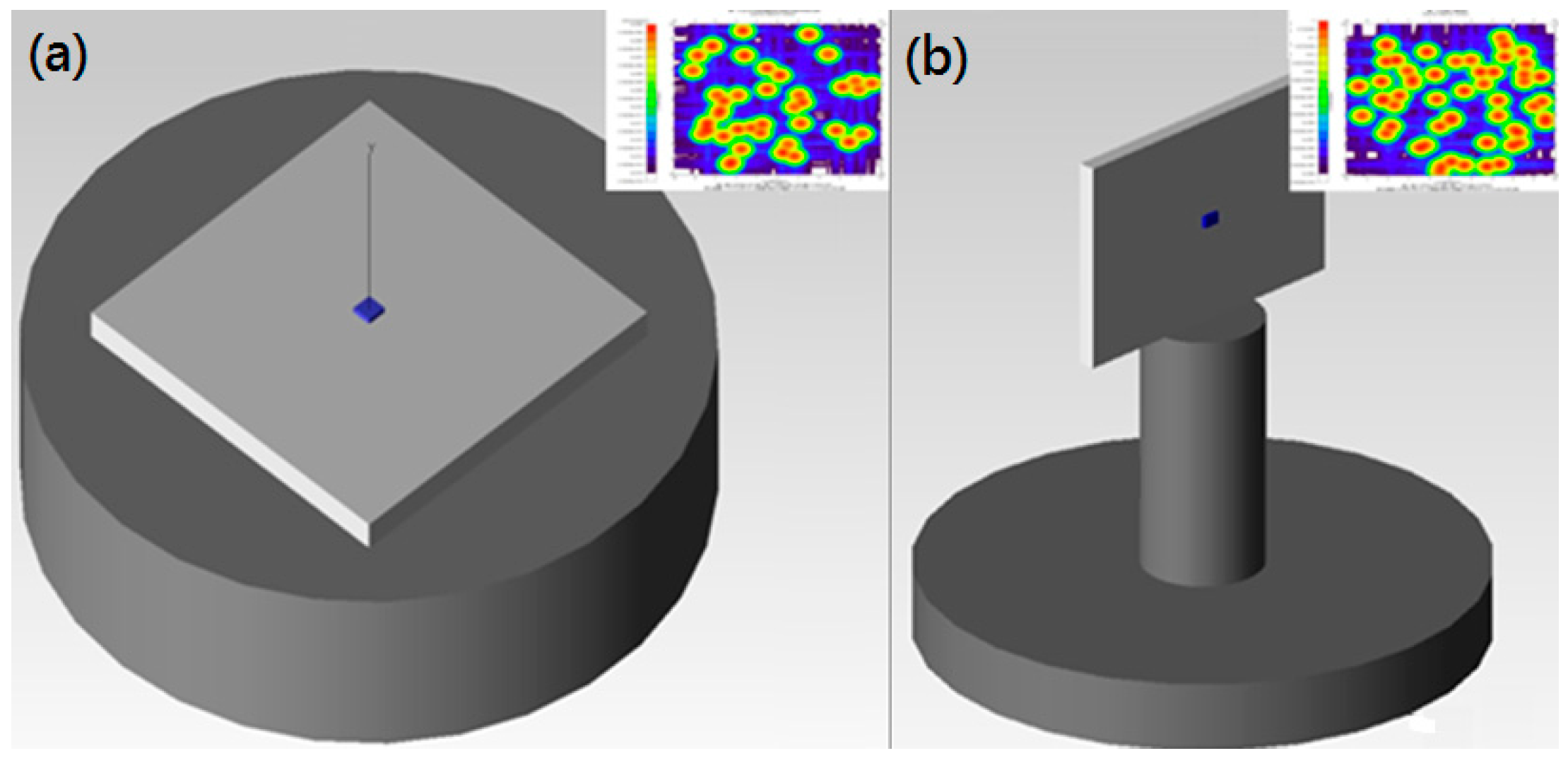
2. Experimental and Simulation

As shown in Figure 1, both the traditional and proposed FCLED mounting structures have been demonstrated. First, the TracePro software (Lambda Research Corporation, Littleton, MA, USA, 2015) is used to simulate the light output efficiency of our proposed FCLED mounting model with a transparent submount, and compares it with that of the traditional style of FCLED mounting on a non-transparent submount. Later, we measure the submount transparency and light output power of FCLED samples mounted on different substrates, respectively. Afterwards, these results are used to correlate with the experimental heat dissipation results measured using an infrared (IR) spectrometer (FLIR Systems, Wilson, OR, USA). The thermal results are also verified with the simulation results using ANSYS 14 (ANSYS, Inc., Canonsburg, PA, USA, 2015).
The TracePro software is used to display the advantages of using the transparent submounts when compared to the traditional style of LEDs on non-transparent submounts, as shown in Figure 1.
The above results shown in Figure 1 were simulated to show the corresponding number of light rays with a constant radius of the integrated sphere, and the corresponding lumen flux was calculated. During the simulation, we took three cases into consideration: the traditional model with the Si submount, and the proposed structure with glass and sapphire as submounts.
As shown in Figure 2 (the simulation result), we can see that the proposed mounting LEDs yield high-output luminous flux as compared to the traditionally mounted LED. This is because the total number of emitting rays is larger for the transparent mounting system which has no rays blocked by the non-transparent traditional submount.
In this experiment, three different submount materials are employed for the LEDs’ flip chip package. They are glass, double side burnish (DSB) sapphire and silicon. All the samples were cleaned using Radio Corporation of America (RCA) cleaning processes, and followed by the metallization processes which are sputtered with 30 nm Cr and 120 nm Au. Finally, the photolithographic processes for contact electrode formation were carried out and the LED chips flip chip bonding are performed. LEDs adopted here had a size of 1 mm by 1 mm square and were from Epi-star Co. (Hsinchu, Taiwan) Those LEDs exhibit an epitaxial structure of a thin nucleation layer, a 2 nm Si-doped GaN layer, five periods of InGaN/GaN multi-quantum wells (MQWs) with a well thickness of 2.4 nm and a barrier thickness of 10 nm, a 20-nm-thick Mg-doped p-AlGaN layer and a 150-nm-thick Mg-doped p-GaN layer, respectively. Before the flip chip process, a Kulicke & Soffa 4522 series Wire Bonder (Kulicke & Soffa, Singapore) was used to make bumps for the electrode connection. Once the samples were ready, optical parameters of the corresponding LEDs were measured using Integrating sphere (AMA Optoelectronics) SLM-20T (AMA Optoelectronics Co., Ltd., Taiyuan, Taiwan). The light intensity (output lumens), color rendering index (CRI), correlated color temperature (CCT), and wavelengths at different bias currents, etc., were measured. Then a thermal imaging system, FLIR SC 620 (IR) (FLIR Systems, Wilson, OR, USA), was employed to take the corresponding thermal images. During measurements, these samples were kept on the specimen holder and current was applied with a constant current source. The thermal images were captured using a thermal video system which exhibits a recording computer. These images were later used to verify our experimental results with the simulation results from ANSYS. To avoid extra interference parameters such as the temperature dependence of the phosphors, all the chips adopted in this research were bare blue light LED dies.

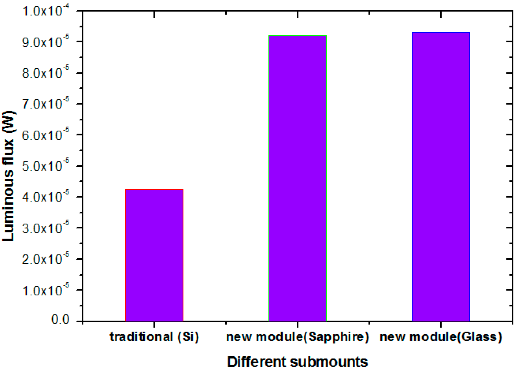
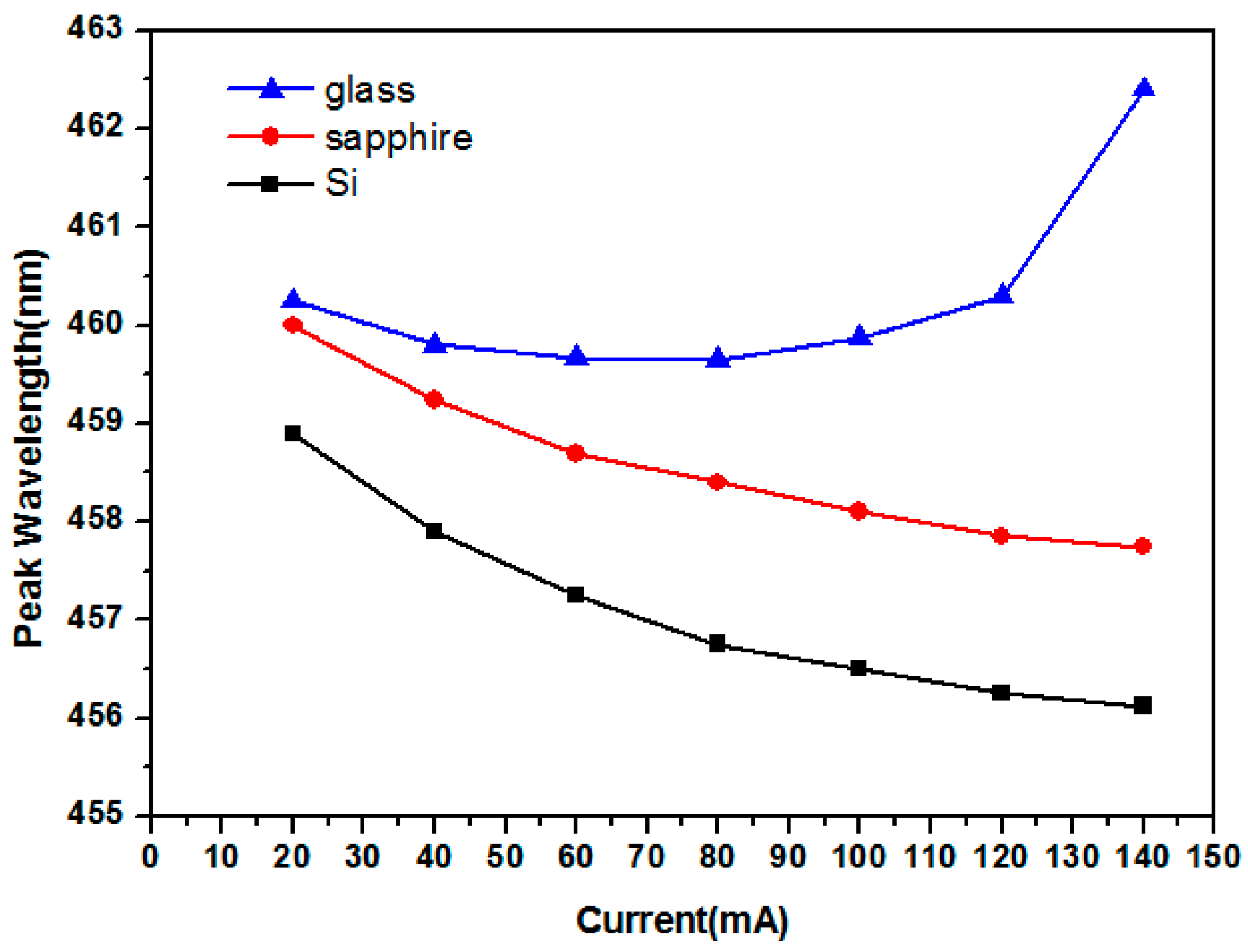
3. Results and Discussions

The optical output intensity of the FCLEDs mounted on different submounts was measured as a function of the driving current, i.e., L–I curves as shown in Figure 3. It was observed that FCLEDs mounted on the DSB sapphire submount had the highest lumens at 150 mA and the LEDs mounted on the silicon exhibited the lowest output values. As to the glass-mounted LEDs, their performance was in between. There are some special tendencies that need to be emphasized: at a low bias current region, due to the transparent property of the glass, its performance was close to that of the DSB samples; at a high current operation region, the heat accumulation–induced droop phenomenon is clearly observed.
Thus, these results are thought to be due to the combination effects of both the transparency and thermal conductivity of each submount, respectively. Although the heat-conducting Si submount shown here exhibits a linear IV curve without any droop phenomenon, it still showed a disadvantage for realizing a high-brightness LEDs FC mounting when compared to those samples mounted on transparent sapphire or glass. The FCLEDs mounted on the DSB sapphire substrate showed a light output power of 0.12 W at a current of 140 mA, which is comparable to the results from other groups [26,27]. FCLEDs mounted on DSB sapphire showed an 80% increase in the light output power when compared to its non-transparent counterpart Si with good thermal conductivity. Glass and sapphire both are transparent substrates, and at a small bias current, the transparent submount dominates the light extraction efficiency. Therefore, the output from LEDs mounted on glass is almost consistent with the LEDs mounted on DSB sapphire. However, due to the thermal conductivity difference, the glass-mounted LEDs’ output power intensity at a high current operation region starts to droop, which implies that at a high current operation region the thermal conductivity dominates.
In general, the LED thermal accumulation behaviors can be deduced from the shift of the corresponding light emission wavelength spectra. Thus, Figure 4 is further focused on the respective light spectra for FCLEDs on different submounts at varying operation currents. From Figure 4, a clear shift in the peak wavelength for different samples with the varying currents can be seen. In the GaN-based blue LED, the common blue shift in the low-injected-current region and good thermal dissipation samples are obtained for both Si and DSB samples. However, at a high-injected-current region the glass sample showed a serious red shift.
To summarize the results of Figure 4, blue LEDs are used in this experiment, and their peak wavelength mostly revolves between 459 nm to 460 nm. As shown in Figure 4, it is observed that the peak wavelength goes on decreasing (blue shift) for FCLEDs mounted on sapphire and silicon which both have good thermal conductivity. However, the peak wavelength variation for FCLEDs mounted on glass, at a region of higher than 100 mA, showed a red shift from 460.4 nm to 462.4 nm which is believed to be due to the thermal accumulation.
For a driving current less than 100 mA, a small blue shift was observed for FCLED on Si and sapphire submounts due to the band-filling effect of the localization energy states caused by indium composition fluctuation in the InGaN multiple quantum wells, which is also known as the quantum confined Stark effect (QCSE) [28]. The Si and sapphire have a thermal conductivity much higher than that of glass, and thus provide a good heat sink. Thermal conductivities used in the above ANSYS simulation for glass, Si and sapphire are 1.05 W/m·°C, 124 W/m·°C and 35 W/m·°C, respectively, as mentioned in the ANSYS engineering toolbox. Due to the excessive heat accumulation in LEDs on glass substrates, the light output intensity drops and a red shift in the peak wavelength was observed. Therefore, we can see that the best choice of submount in this work is sapphire, which exhibits a good transparent property and also serves as a heat-sinking material.
To further confirm our observations and assumptions, the thermal dissipation capability of fabricated samples was investigated using a thermal imager. The power was applied to all the samples using a constant current source and their thermal images were captured by a thermal imager camera. From the inset of Figure 5, one can see that a large amount of heat accumulated near the electrode area of the submounts. The results were then compared with the ANSYS simulation results.
In ANSYS, a model is designed and the LED is taken as a point heat source. Volume and thermal conductivity are the two most important parameters for modeling and simulation. The experimental and simulation results are compared and found to have good agreement with one another. It is observed that Si dissipates heats much better than sapphire and glass because the thermal conductivity of Si is the highest among these three materials. Glass dissipates the least amount of heat due to its low thermal conductivity. LEDs mounted on the sapphire substrate showed good results in our test and we believe there is still potential for improvement. As a rule of thumb, the higher the thermal conductivity is, the more potential there is as a candidate for the FCLEDs’ transparent submounts. As shown in Figure 5, our ANSYS simulation results are in accordance with our experimental observations.
From the experimental results, the numerical data for the variation of temperature (at the point where the LED was mounted) at different operation currents for different submounts can be found, as shown in Figure 6. It can be seen that although glass has a very high transparency, due to its low thermal conductivity it is not able to dissipate heat, and this results in a huge accumulation of heat which reduces the light output of the correspondent FCLED.

4. Conclusions

In conclusion, the optical properties of the FCLEDs mounted on different submounts are investigated. FCLEDs on transparent sapphire or glass submounts have a better light extraction ratio. As compared to the non-transparent counterpart Si submount, FCLEDs mounted on transparent sapphire or glass showed an 80% increase in light output power, which makes them promising candidates for future solid-state light applications. However, there is a heat dissipation issue that needs to be solved. All these electrical and optical observations are verified by the thermal image results as well as the ANSYS simulation data. Among these three submounts, sapphire came out to be the best option for FCLED fabrication, as it adopted both a good transparency and a good thermal conductivity. If the heat problem of the glass submount can be solved in the future, we believe there will be a huge demand for transparent glass–mounted LEDs due to the high light extraction ratio when compared to the traditional mounting method.

Acknowledgments

This work was supported by the Ministry of Science and Technology of Taiwan, Project No. 104-2221-E-182-038.

Author Contributions

Preetpal Singh organized and designed the experiment procedures; Chih-Teng Hou and Ting-Yu Chao performed the experiments and analyzed the data; Cher-Ming Tan and Chao-Sung Lai contributed the measurement tools; Der-Hwa Yeh and Liann-Be Chang supported the measurement results and wrote this paper; All authors read and approved the final version of the manuscript to be submitted.

Conflicts of Interest

The authors declare that there is no conflict of interests regarding the publication of this paper.

References

  1. Chang, L.B.; Yeh, D.H.; Hsieh, L.Z.; Zeng, S.H. Enhanced modulation rate in platinum-diffused resonant-cavity light-emitting diodes. J. Appl. Phys. 2005. [Google Scholar] [CrossRef]
  2. Leem, Y.-C.; Seo, O.; Jo, Y.-R.; Kim, J.H.; Chun, J.; Kim, B.-J.; Noh, D.Y.; Lim, W.; Kim, Y.-I.; Park, S.-J. Titanium oxide nanotube arrays for high light extraction efficiency of GaN-based vertical light-emitting diodes. Nanoscale 2016, 8, 10138–10144. [Google Scholar] [CrossRef] [PubMed]
  3. Zhu, P.; Tansu, N. Effect of packing density and packing geometry on light extraction of III-nitride light-emitting diodes with microsphere arrays. Photon. Res. 2015, 3, 184–191. [Google Scholar] [CrossRef]
  4. Zhu, P.; Tansu, N. Resonant cavity effect optimization of III-nitride thin-film flip-chip light-emitting diodes with microsphere arrays. Appl. Opt. 2015, 54, 6305–6316. [Google Scholar] [CrossRef] [PubMed]
  5. Zhu, P.; Tan, C.-K.; Sun, W.; Tansu, N. Aspect ratio engineering of micro lens arrays in thin-film flip-chip light-emitting diodes. Appl. Opt. 2015, 54, 10299–10303. [Google Scholar] [CrossRef] [PubMed]
  6. Tsai, M.Y.; Tang, C.Y.; Yen, C.Y.; Chang, L.B. Bump and under fill effects on thermal behaviors of flip-chip LED packages: Measurement and modeling. IEEE Trans. Device Mater. Reliab. 2014, 14, 161–168. [Google Scholar] [CrossRef]
  7. Chang, L.B.; Chiang, K.L.; Chang, H.Y.; Jeng, M.J.; Yen, C.Y. Electrostatic reliability characteristics of GaN flip-chip power light-emitting diodes with metal-oxide-silicon submount. IEEE Trans. Electron. Devices 2010, 57, 119–124. [Google Scholar] [CrossRef]
  8. Chang, L.B.; Shiue, C.C.; Jeng, M.J. The reflectivity enhancement of Ni/Ag/(Ti or Mo)/Au ohmic contact for flip-chip LED application. In Proceedings of the 15th IEEE International Conference on Advanced Thermal, Catania, Italy, 2 October 2007.
  9. Ju, L.Y.; Chiu, C.H.; Ke, C.C.; Lin, P.C.; Lu, T.C.; Kuo, H.C.; Wang, S.C. Study of the excitation power dependent internal quantum efficiency in InGaN/GaN LEDs grown on patterned sapphire substrate. IEEE J. Sel. Top. Quantum Electron. 2009, 15, 1137–1143. [Google Scholar]
  10. Fujii, T.; Gao, Y.; Sharma, R.; Hu, E.L.; DenBaars, S.P.; Nakamura, S. Increase in the extraction efficiency of GaN-based light-emitting diodes via surface roughening. Appl. Phys. Lett. 2004, 84, 855–857. [Google Scholar] [CrossRef]
  11. Lee, S. Optimum design and selection of heat sinks. IEEE Trans. Compon. Packag. Manuf. Technol. 1995, 18, 812–817. [Google Scholar] [CrossRef]
  12. Mashford, B.S.; Stevenson, M.; Popovic, Z.; Hamilton, C.; Zhou, Z.; Breen, C.; Steckel, J.; Bulovic, V.; Bawendi, M.; Sullivan, S.C.; et al. High-efficiency quantum-dot light-emitting devices with enhanced charge injection. Nat. Photonics 2013, 7, 407–412. [Google Scholar] [CrossRef]
  13. Arik, M.; Petroski, J.; Weaver, S. Thermal challenges in the future generation solid state lighting applications: Light emitting diodes. Int. Soc. Conf. Ther. Phenom. 2002. [Google Scholar] [CrossRef]
  14. Chen, S.H.; Tan, C.M.; Tan, E.; Kong, J. Effects of carbon loading on the performance of functionalized carbon nanotube polymer heat sink for ultra high power light-emitting diode. In Proceedings of the 2013 IEEE 5th International on Nanoelectronics Conference, Singapore, 2–4 January 2013; pp. 81–84.
  15. Pan, C.-C.; Koslow, I.; Sonoda, J.; Ohta, H.; Ha, J.-S.; Nakamura, S.; DenBaars, S.P. Vertical stand transparent light-emitting diode architecture for high-efficiency and high-power light-emitting diodes. Jpn. J. Appl. Phys. 2010. [Google Scholar] [CrossRef]
  16. Kim, J.Y.; Na, S.I.; Ha, G.Y.; Kwon, M.K.; Park, I.K.; Lim, J.H.; Park, S.J. Thermally stable and highly reflective AgAl alloy for enhancing light extraction efficiency in GaN light-emitting diodes. Appl. Phys. Lett. 2006. [Google Scholar] [CrossRef]
  17. Peng, W.C.; Wu, Y.C.S. Enhanced performance of an InGaN-GaN light-emitting diode by roughening the undoped-GaN surface and applying a mirror coating to the sapphire substrate. Appl. Phys. Lett. 2006. [Google Scholar] [CrossRef]
  18. Katona, T.M.; Speck, J.S.; Denbaars, S.P. Effect of the nucleation layer on stress during cantilever epitaxy of GaN on Si (111). Phys. Stat. Sol. 2002, 194, 550–553. [Google Scholar] [CrossRef]
  19. Krost, A.; Dadgar, A. GaN-based optoelectronics on silicon substrates. Mater. Sci. Eng. B 2002, 93, 77–84. [Google Scholar] [CrossRef]
  20. Zhang, B.; Liang, H.; Wang, Y.; Feng, Z.; Ng, K.W.; Lau, K.M.J. High-performance III-nitride blue LEDs grown and fabricated on patterned Si substrates. Cryst. Growth 2007, 298, 725–730. [Google Scholar] [CrossRef]
  21. Dadgar, A.; Clos, R.; Strassburger, G.; Schulze, F.; Veit, P.; Hempel, T.; Bläsing, J.; Krtschil, A.; Daumiller, I.; Kunze, M.; et al. Strains and Stresses in GaN Heteroepitaxy—Sources and Control. Adv. Solid State Phys. 2004, 44, 313–325. [Google Scholar]
  22. Feltin, E.; Dalmasso, S.; Mierry, P.D.; Beaumont, B.; Lahrèche, H.; Bouillé, A.; Haas, H.; Leroux, M.; Gibart, P. Green InGaN light-emitting diodes grown on silicon (111) by metal organic vapor phase epitaxy. Jpn. J. Appl. Phys. 2001, 40, L738–L740. [Google Scholar] [CrossRef]
  23. Shih, C.F.; Chen, N.C.; Chang, C.A.; Liu, K.S. Blue, green and white InGaN light-emitting diodes grown on Si. Jpn. J. Appl. Phys. 2005, 44, L140–L143. [Google Scholar] [CrossRef]
  24. Egawa, T.; Zhang, B.; Ishikawa, H. High performance of InGaN LEDs on (111) silicon substrates grown by MOCVD. IEEE Electron Device Lett. 2005, 26, 169–171. [Google Scholar] [CrossRef]
  25. Li, J.; Lin, J.Y.; Jiang, H.X. Growth of III-nitride photonic structures on large area silicon substrates. Appl. Phys. Lett. 2006. [Google Scholar] [CrossRef]
  26. Wierer, J.J.; Steigerwald, D.A.; Krames, M.R.; O’Shea, J.J.; Ludowise, M.J.; Christenson, G.; Shen, Y.-C.; Lowery, C.; Martin, P.S.; Subramanya, S.; et al. High-power AlGaInN flip-chip light-emitting diodes. Appl. Phys. Lett. 2001, 78, 3379–3381. [Google Scholar] [CrossRef]
  27. Mukai, T.; Yamada, M.; Nakamura, S. Current and temperature dependences of electroluminescence of InGaN-based UV/Blue/Green light-emitting diodes. Jpn. J. Appl. Phys. 1998, 37, L1358–L1361. [Google Scholar] [CrossRef]
  28. Ding, L.Z.; Chen, H.; He, M.; Jiang, Y.; Lu, T.P.; Deng, Z.; Chen, F.S.; Yang, F.; Yang, Q.; Zhang, Y.; et al. Improved photoluminescence in InGaN/GaN strained quantum wells. Chin. Phys. Lett. 2014. [Google Scholar] [CrossRef]
Figure 1. Traditional style of flip chip light-emitting diode (FCLED) on non-transparent submounts (a), and proposed transparent mounting of FCLED (b). Inset figures show the simulation flux results for the two mounting styles with silicon or glass, respectively.
Applsci 06 00179 g001
Figure 2. Comparison of luminous flux with different substrates under different mounting technologies.
Applsci 06 00179 g002
Figure 3. L–I curves for the different FCLED samples. The inset figure shows the transparent submount bidirectional LED module.
Applsci 06 00179 g003
Figure 4. Peak wavelength variation vs. operation current for LEDs mounted on different submounts.
Applsci 06 00179 g004
Figure 5. Comparison between experimental and ANSYS simulation results. The inset figure shows the figures of ANSYS simulation and the IR measurement.
Applsci 06 00179 g005
Figure 6. Average surface temperature vs. operation current for different submounts.
Applsci 06 00179 g006

