Distributed Bragg Reflectors for GaN-Based Vertical-Cavity Surface-Emitting Lasers


Department of Electrical Engineering, Yale University, New Haven, CT 06520, USA
*
Author to whom correspondence should be addressed.
Appl. Sci. 2019, 9(8), 1593; https://0-doi-org.brum.beds.ac.uk/10.3390/app9081593
Submission received: 14 March 2019
/
Revised: 12 April 2019
/
Accepted: 15 April 2019
/
Published: 17 April 2019
(This article belongs to the Special Issue Group III-V Nitride Semiconductor Microcavities and Microemitters)
Abstract
:Featured Application
GaN based vertical-cavity surface-emitting lasers.
Abstract
A distributed Bragg reflector (DBR) is a key building block in the formation of semiconductor microcavities and vertical cavity surface emitting lasers (VCSELs). The success in epitaxial GaAs DBR mirrors paved the way for the ubiquitous deployment of III-V VCSELs in communication and mobile applications. However, a similar development of GaN-based blue VCSELs has been hindered by challenges in preparing DBRs that are mass producible. In this article, we provide a review of the history and current status of forming DBRs for GaN VCSELs. In general, the preparation of DBRs requires an optimization of epitaxy/fabrication processes, together with trading off parameters in optical, electrical, and thermal properties. The effort of epitaxial DBRs commenced in the 1990s and has evolved from using AlGaN, AlN, to using lattice-matched AlInN with GaN for DBRs. In parallel, dielectric DBRs have been studied since 2000 and have gone through a few design variations including epitaxial lateral overgrowth (ELO) and vertical external cavity surface emitting lasers (VECSEL). A recent trend is the use of selective etching to incorporate airgap or nanoporous GaN as low-index media in an epitaxial GaN DBR structure. The nanoporous GaN DBR represents an offshoot from the traditional epitaxial approach and may provide the needed flexibility in forming manufacturable GaN VCSELs. The trade-offs and limitations of each approach are also presented.
1. Introduction
Propagation of electromagnetic waves in periodic media has produced a plethora of intriguing natural phenomena and useful applications. The natural world provides a rich collection of examples of bio-photonic structures including the wing of the Morpho butterfly [1,2], peacock feathers [3], the striking colors of flower petals [4], the iridescent luster from nacre shells [5], and light confinement in C. Wailesii cell wall [6,7], to name just a few [8]. Technological applications of periodic photonic structures include diffraction of X-rays in crystals, wavelength selection in fiber gratings, physical sensors and manipulation of light in photonic crystals. Distributed Bragg reflectors (DBRs), sometimes called Bragg mirrors or quarter wavelength stacks, represent one of the simplest periodic photonic structures. In a multi-layered structure with a periodic high-low contrast in the optical index of refraction, when the thicknesses of the individual layers equal to a quarter of the optical wavelength (λ/4) (or more broadly the odd multiples of a quarter wavelength such as 3λ/4, 5λ/4, etc.), the successive reflections at each interface cause constructive interference for the reflective wave around the Bragg wavelength λ, and the multiple layers act as a mirror with a tunable reflectivity and bandwidth.
Multi-layered Bragg mirror structures were first demonstrated around 1940 with coatings of alternate dielectric layers [9,10,11]. These dielectric structures contributed to the formation of high-Q cavity in the early development of lasers. With advances in modern epitaxial techniques such as molecular beam epitaxy (MBE) and organometallic vapor phase epitaxy (OMVPE) in the 1970s, tremendous progress was made in the growth of AlGaAs heterostructures with atomic layer control. Single crystalline, epitaxial DBR mirrors were demonstrated in the 1980s [12], which was arguably the most important factor that led to the demonstrations of room-temperature of continuous-wave operation of vertical cavity surface-emitting lasers (VCSELs) in the infrared wavelengths [13,14]. Currently III-V VCSELs play an important role in data communications, mobile sensing, and many emerging applications [15], with a projected global market of 3.89 billion USD by 2023 [16].
Since early 1990s, GaN-based blue light-emitting diodes (LEDs) and laser diodes (LDs) have revolutionized contemporary technologies in illumination and display. The technology of blue VCSELs, however, has not reached the same level of maturity. Beginning in the late 1990s there were reports of optically-pumped InGaN VCSELs [17,18]. More than 10 years later, electrically-injected InGaN VCSELs were demonstrated in 2008 [19,20]. At the preparation of this review article, after another 10 years of pursuit, GaN VCSELs have yet to be commercialized in spite of encouraging progress. It is accepted that a key component and bottleneck in the GaN VCSEL technologies is the preparation of DBR mirrors, in particular the DBR mirror on the substrate side.
With the increasing interest in and reports of GaN VCSELs as a backdrop, this article aims to provide a review and assessment of this key element for VCSEL with an intention that, by outlining the experiences learned and remaining challenges, new breakthroughs and innovations will lead to the ubiquitous deployment of short-wavelength visible VCSELs in lighting, display, communication and other applications. This article is arranged in the following way, in Section 2 we will first review the different techniques in preparing DBR mirrors for VCSELs, followed by a discussion of the properties of and design constraints in fabricating DBR mirrors. Turning our focus to specific embodiments of DBR mirrors for GaN VCSELs, we will then review the development of both epitaxial (Section 3) and dielectric DBR mirrors (Section 4) and highlight the state of the art. The article is concluded with new approaches of using airgap or nanoporous DBR mirrors to tackle this challenging yet crucial problem for GaN VCSELs (Section 5).
2. Fabrication Techniques and Design Considerations of Distributed Bragg Reflectors (DBRs)
2.1. Fabrication Techniques of DBRs
Prior to 1980s, all of the highly reflective DBR mirrors were produced by the deposition of amorphous dielectric layers with oxides (SiO2, HfO2, and Ta2O5), nitrides (SiNx), and fluorides (MgF2, …) [21]. This was a branch in the mature field of optical coating [22] for interference filters, anti-reflective coatings, mirrors, and absorbers. In this article we refer this approach of fabricating DBR mirrors as non-epitaxial or dielectric DBRs, interchangeably. After the conceptual proposal of VCSEL by K. Iga in 1977 [23], dielectric DBRs and/or metal reflectors were the only options toward the realization of this novel device [24,25,26,27]. However, since the semiconductor gain region (a double heterostructure, DH, or multiple quantum wells, MQWs) of a VCSEL needs to be prepared epitaxially on a single crystalline substrate, major fabrication efforts had to be exerted to remove the single crystalline substrates, or to expose the backside of the active region, and to coat both the top and bottom surfaces of the gain region with non-epitaxial DBR mirrors. During this time the overall pursuit of VCSEL devices can be considered more of a laboratory curiosity than for technology development.
With the advances in modern epitaxial technologies for III-V compound semiconductors, epitaxial growth of AlGaAs/GaAs DBR mirrors was first demonstrated in 1983 using MBE [12] and subsequently with OMVPE [28]. Epitaxial DBRs enable a continuous growth of a full VCSEL structure to greatly simplify the fabrication process. Furthermore, semiconductor epitaxial DBRs could be made electrically and thermally conductive, thus producing significant benefits to the VCSEL performance. With these stated benefits, nevertheless, the pathway to manufacturable DBRs is by no means straightforward. In the epitaxial growth of DBRs, an implicit requirement is the hetero-epitaxy of two λ/4 layers having sufficiently contrasting dielectric property in order to induce appreciable reflection at each interface. Several technical challenges are often reported in the epitaxial production of DBR mirrors:
(1) In the case where the DBR layers consists of different cation elements such as Al, Ga, and or In, the difference in diffusion properties of surface adatoms [29] needs to be factored into growth design to ensure two-dimensional growth modes [30,31].
(2) In the case where the DBR layers consists of different anion elements including As, P, or Sb, the difference in surface reactivity and sticking coefficients needs to be carefully monitored and controlled [32,33],
(3) In the use of ternary or quaternary alloys as DBR layers, it is crucial to maintain uniformity in compositions and thicknesses across the entire wafer [34,35,36],
(4) As a result of (1)–(3), a need to use different, and sometimes compromised growth conditions for the two layers, which often results in interfacial disorder or deterioration in surface morphology [37,38], and
(5) Last but not least, a difference in lattice parameters between the constituent layers leading to high-tensile or compressive strains during the growth of DBRs [39,40].
Given these challenges, growth of highly-reflective DBRs is often considered both the most challenging task and a symbolic gauge of maturity in epitaxy for a specific heteroepitaxial system. We also want to add that the success in epitaxial DBRs has laid a foundation for modern integrated optics [41] and even quantum optics [42].
2.2. Optical Design Consideration
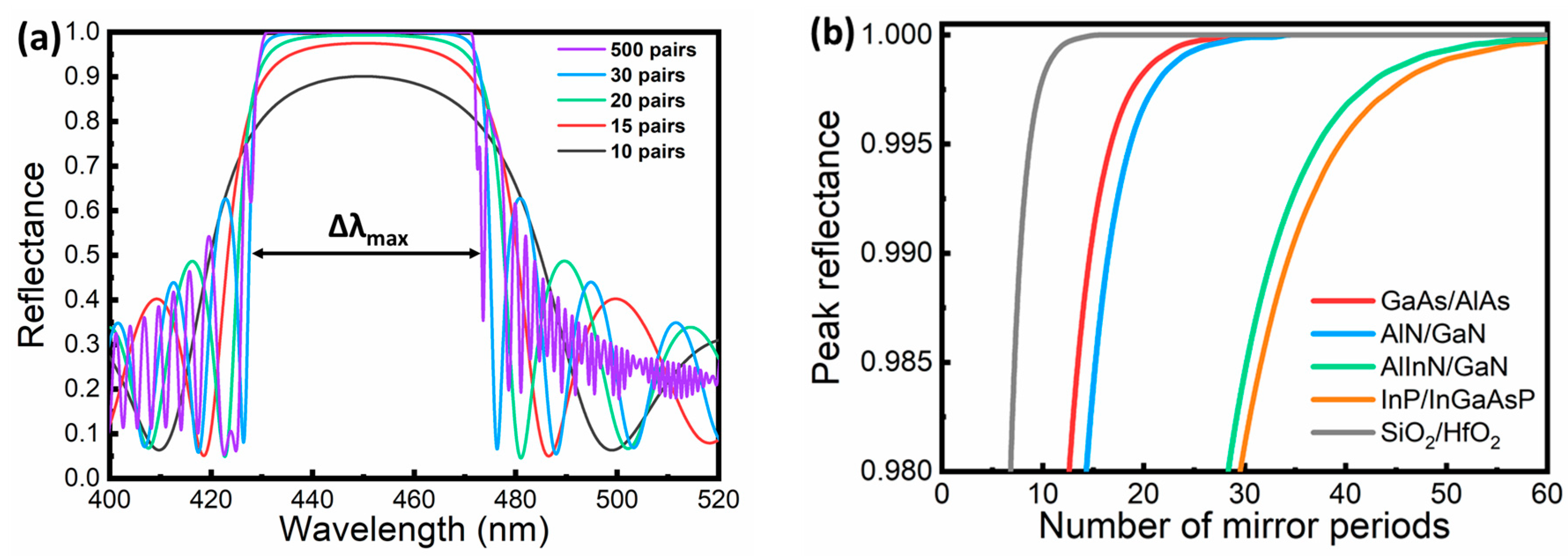
The optical principle of a DBR mirror is based on successive Fresnel reflection at normal incidence at interfaces among two alternating layers with refractive indices n1 and n2: . When the optical thickness of each layer is maintained at a quarter wavelength (λ/4) thick, the path difference between reflections from successive interfaces equals to half the wavelength (λ/2), or 180° out of phase. However, since reflections (r) at successive interfaces have alternating signs to compensate the 180° phase shift from the differences in path length, all the reflected components interfere constructively, and the cumulative reflection can be enhanced by design. The reflectance spectrum of a DBR can be calculated using the transmission matrix theory [43]; an example of the calculated spectrum of an AlN (n = 2.15)/GaN (n = 2.52) DBR with different number of pairs is shown in Figure 1a.
As the number of pairs increases, the shape of the reflectance spectrum evolves from a rounded peak to a perfect rectangular spectral band, with the peak of reflectance increasing according to the following equation [45]:
where m is the number of layer pairs, and and are the optical indices of the materials with lower and higher indices of refraction, respectively. According to Equation (1), we plot in Figure 1b the peak reflectivity versus the number of DBR pairs m for several epitaxial systems consisting of GaAs, InP, and GaN, and a dielectric DBR from SiO2/HfO2 for comparison. For a low-threshold VCSEL operation, a mirror reflectivity of > 99.5% is often required to reduce the round-trip mirror loss. Dielectric DBRs in general provides the most ideal reflectance curve with relatively few numbers of DBR pairs (m ~ 10). AlAs/GaAs and AlN/GaN have a sufficient index contrast to reach high reflectance in ~20 pairs of DBR. In the other two cases epitaxial DBRs requires more than 40 pairs for high reflectance. In practice, the number of pairs calculated based on Equation (1) gives a lower bound in experimental design; additional pairs are often required to offset other non-idealities such as surface roughness or thickness variations.
As seen in Figure 1a, the width of the high-reflectance band of DBR mirrors, Δλmax, is an important design parameter for VCSEL. The stopband width of DBR mirror is expressed as [45]:
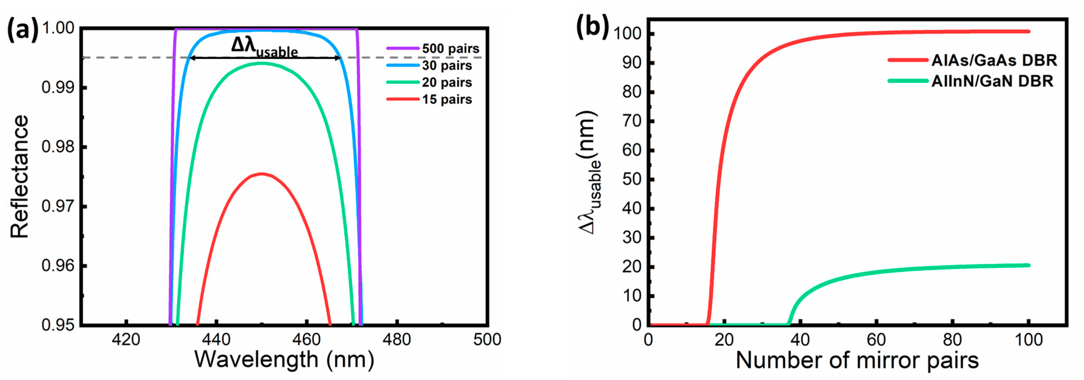
The Δλmax given in Equation (2) specifies the full width at half maxima of the reflectance of a DBR mirror when the number of pairs approaches infinity. Δλmax is proportional to the Bragg wavelength λ and is sensitively affected by the index contrast (Δn = ). Thus, a higher Δn is very desirable in DBR fabrication for both a high peak reflectance (from Equation (1)) and a wide stopband width (from Equation (2)). In the practical implementation with a finite number of DBR pairs, the actual “usable” reflectance bandwidth, Δλusable, for a high performance VCSEL (for example for R > 0.995) can be a factor of 2 to 3 times narrower than Δλmax. Figure 2a provides a close-up plot of the evolution of spectrums in Figure 1a, focusing on the high reflectance portion. As the number of pairs increases, the peak of the reflectance spectrum will reach a practical threshold (say, 0.995) above which Δλusable becomes greater than 0. As the number of DBR pairs continues to increase, Δλusable gradually increases toward the respective Δλmax, defined by Equation (2). Such a transition of Δλusable is plotted in Figure 2b here for two lattice-matched material systems, AlAs/GaAs and AlInN/GaN. The large difference of Δλusable in Figure 2b can be explained by Equation (2) due to approximately a 2× difference in wavelength and almost 3× difference in Δn.
2.3. Transport Properties: Electrical and Thermal Conductivities
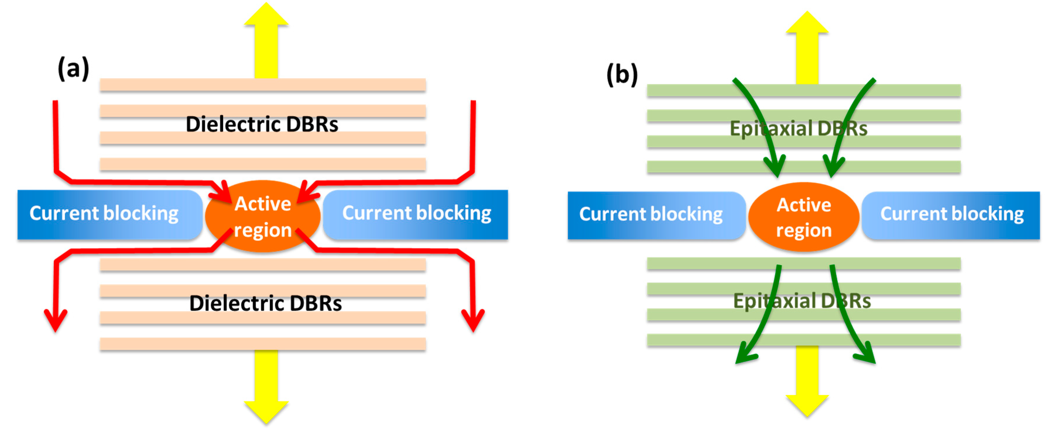
The choice between non-epitaxial and epitaxial DBRs has a significant implication on the resulting device configuration. In the case of non-epitaxial DBRs, complex processing techniques are required to encase the epitaxial gain/active region with top and bottom dielectric DBRs (Figure 3a). Since non-epitaxial DBRs are typically electrically insulating, one needs to develop schemes for lateral current injection (shown schematically as red arrows in Figure 3a) through intra-cavity current spreading layers. These layers are necessarily thin yet heavily doped, often representing a trade-off between electrical impedance and optical absorptive loss. The issue of joule heating with lateral current injection is exacerbated by the rather poor thermal conductivities of dielectric DBRs (0.1~2 W/m-K). Thermal transport in non-epitaxial DBRs is sometimes improved by lengthening the cavity with additional n-type layers to facilitate lateral heat flow [46,47], or by incorporating sophisticated CMOS-like 3D heat-sinking schemes through the dielectric DBRs [48].
Epitaxial semiconductor DBR mirrors offer good electrical conductivities and improved thermal conductivities over their dielectric counterpart. In the best case of the mature Al(Ga)As/GaAs system, electrical resistance and thermal conductivity of 10−3 Ω-cm and 300 W/m-K, respectively, can be achieved [49,50]. Conductive DBRs enable vertical current injection into the gain region of a VCSEL for best current uniformity and device impedance (Figure 3b). This is the configuration nearly all commercial VCSELs employ. However, injecting current though the epitaxial DBR comes with its own challenges. The stacking of alternating layers of different bandgaps, create potential barriers which inhibit carrier flow and increase the overall DBR resistance. Several techniques have been implemented, such as interfacial doping [51] or interfacial alloy grading [52,53], however, these implementations often come on the expense of the optical reflectivity and thermal properties of the DBRs and a trade-off between the different properties is usually decided.
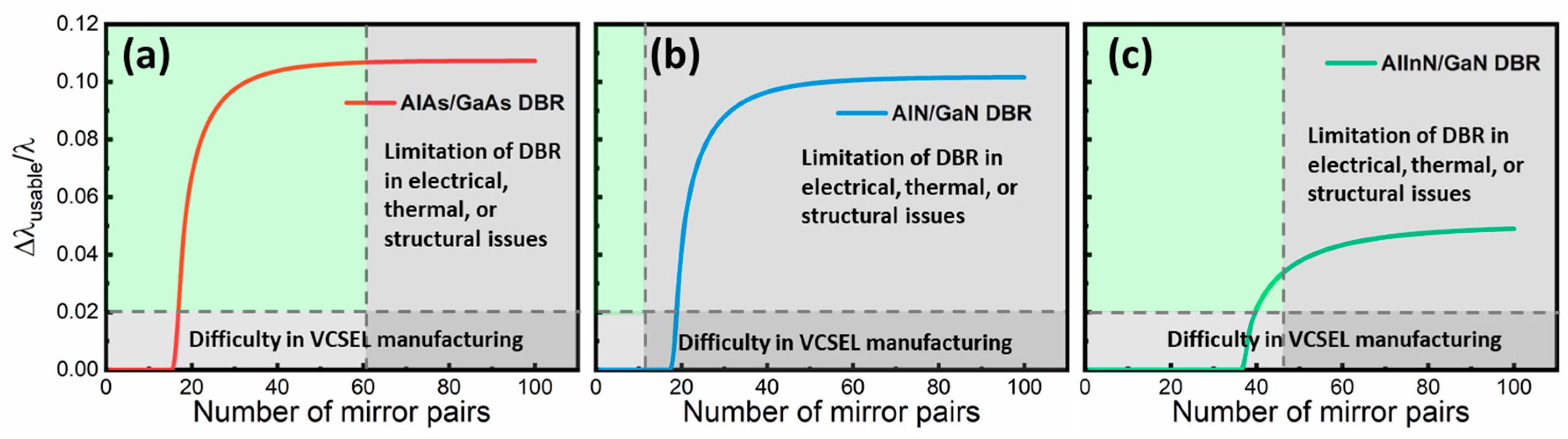
While the epitaxial DBR configuration is a clear preference and the mainstream for the mature infrared and red VCSEL industry, the choice of DBR for AlGaInN-based VCSELs remains a debatable subject and represents a tradeoff among optical properties, transport limitation, and ultimately the manufacturability. In Figure 4 we illustrate these design constraints in a qualitative way. As is described in Section 2.2, semiconductor DBRs sometimes have limited Δn and consequently a narrow width of stopband Δλusable. A more pertinent gauge for the manufacturability of VCSELs is not the absolute width of Δλusable, as is shown in Figure 4, but a normalized ratio, which we defined as Δλusable/λ, that needs to be maintained above a certain margin against the non-uniformities and variations that are often inevitable in epitaxy and fabrication processes. For example, for a blue VCSEL emitting at λ = 450 nm, a Δλusable of 9 nm wide, centered around 450 nm, would require the variation of cavity mode (related to the thickness control) and gain peak (related to indium composition and growth rate) to be with ± 1.0% across the wafer to have a sufficient yield of VCSELs. Any deviation across the wafer in thickness or composition that exceeds this 1% margin will substantially change, if not fail, the VCSEL characteristics. Δλusable/λ therefore can be considered the tolerance in process variations in manufacturing VCSELs. In Figure 4 we plot the calculated Δλusable/λ versus m for the AlAs/GaAs (λ = 950 nm) and AlInN/GaN (λ = 450 nm) systems to illustrate this idea, using a value Δλusable/λ = 0.02 as the cutoff below which the process window becomes too narrow for the specific approach to be deemed mass-producible [54]. As the number of DBR pair increases, there will be a practical upper limit defined jointly by opposing factors such as electrical impedance, thermal resistance, and epitaxial strain energy. Such a practical upper bound is labeled as the dashed vertical lines in Figure 4, beyond which the DBR synthesis is no longer deemed manufacturable. The feasibility of a particular choice of DBRs will depend on how much the calculated Δλusable/λ curves traverse the “second quadrant”, or the green quadrant, in Figure 4.
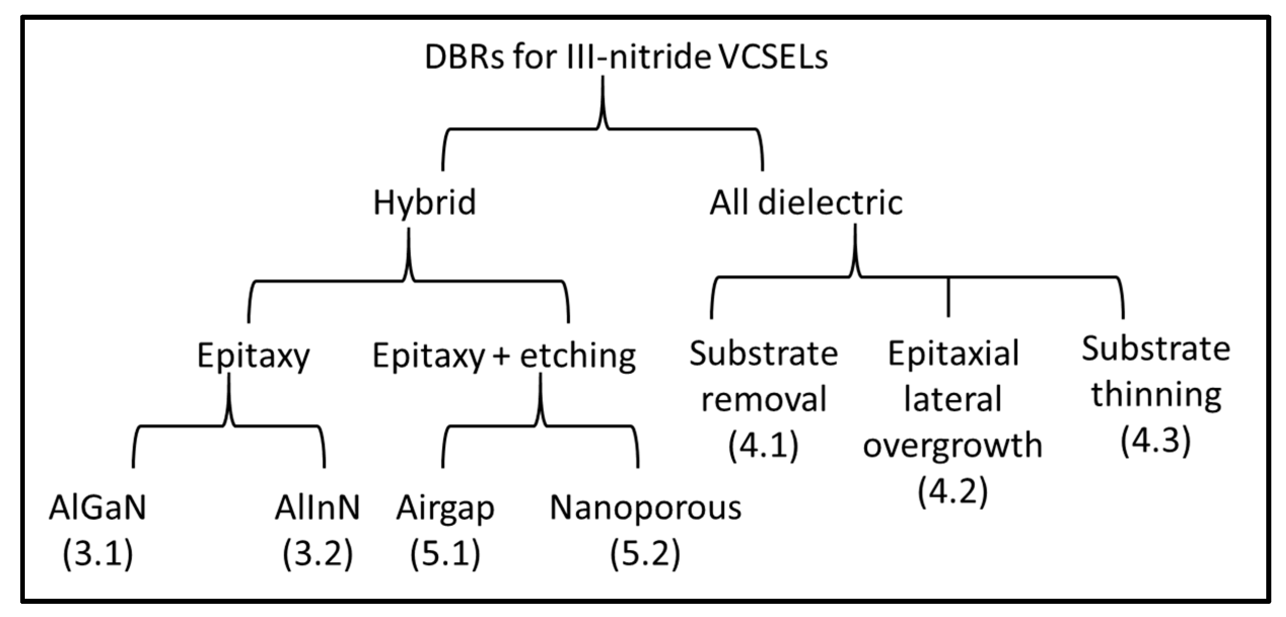
As can be inferred from Figure 4, the range of operation is drastically different from AlAs/GaAs to III-nitride DBRs. The binary AlN/GaN has a high index contrast yet is exceedingly challenging in epitaxy. The lattice-matched AlInN/GaN system can be prepared in principle with more pairs, yet the increased feasibility is somewhat offset by a low index that can be summarized as finding or creating a sweet spot between Figure 4b,c. In the following we will review the history and development of different DBRs in GaN VCSELs. Numerous implementations of DBRs have been reported and are categorized in Figure 5 for clarity. For the III-nitride VCSELs, it is pretty much the consensus that p-type III-nitride epitaxial DBRs cannot be realized in the foreseeable future, so the types of III-nitride VCSELs are divided into either hybrid (dielectric-epitaxial) or all dielectric versions. In our review, we will outline the technical issues associated with growth or fabrication and will discuss the respective strengths and limitations.
3. Epitaxial DBRs for GaN Vertical Cavity Surface-Emitting Lasers (VCSELs)
3.1. Al(Ga)N/GaN DBRs
A lattice mismatching of 2.4% between AlN and GaN introduces excessive tensile or compressive strain and stress (~7 kPa) in AlN/GaN heteroepitaxial layers [55]. Instead of using the two binary ends (AlN and GaN) as the DBR materials, adjusting the AlN or GaN mole fraction in a ternary AlGaN compound can help to reduce the strain accumulation during DBR growth and minimize the possibility of crack formation. However, the index contrast between AlN and GaN is only ~0.34 [56,57]. Using a ternary layer as one of the DBR layers will significantly reduce the index contrast, which then necessitates a large number of AlGaN/GaN pairs (>50 pairs) to achieve a high reflectance.
While the index contrast between AlN and GaN is 0.34, the large lattice mismatch (2.4%) between the two compounds would introduce excessive tensile or compressive strain and stress (~7kPa) within the AlN/GaN heteroepitaxial layers, extremely deteriorating the DBRs properties. Therefore, it is common adjust the AlN and GaNN mole fraction in a ternary AlGaN compound to reduce strain accumulation and minimize the possibility of crack formation. However, due to the lowered refractive index contrast, in an AlGaN/GaN DBR, a large number of pairs (>50) is required to achieve high reflectance, which is indeed not an easy growth task.
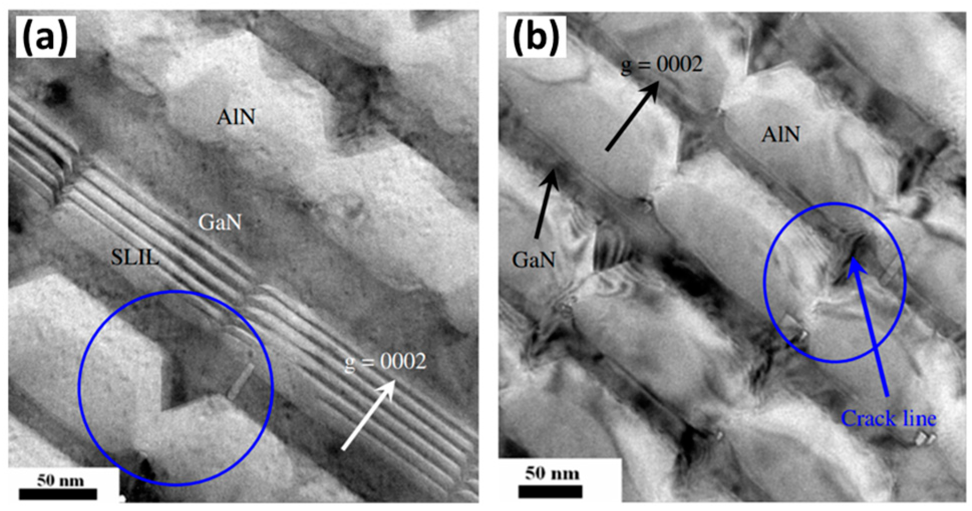
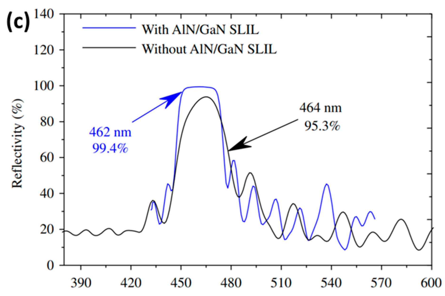
In 1991, Khan et al. [58] reported the first Al0.2Ga0.8N/GaN DBRs in the blue (442 nm) and violet (375 nm) wavelengths. A small amount of Al was used in ternary AlGaN for the ease of growth but compromised the reflectance (80~95%). In 1996, Redwing et al. [59] reported the first optically pumped GaN-based VCSEL with a 10-μm GaN active region sandwiched between 30 pairs of Al0.40Ga0.60N/Al0.12Ga0.88N top and bottom DBRs with reflectances of 93% and 84%, respectively. The low-reflectivity mirrors and a long cavity lead to a very high threshold pumping power (2.0 MW/cm2). To overcome the stress generation and enable growth of a larger number of DBR pairs with good epitaxial quality, several proposals were made using either short-period superlattices (SLs) [60] or thin low-temperature AlN interlayers [61] below or inside the DBRs to release the strain. Between 1999 and 2000, several groups reported optically pumped VCSEL operation using AlGaN/GaN epitaxial DBRs [17,18,62]. The research on AlGaN DBRs continued in subsequent years [60,63,64,65,66,67]. Electrical injection with AlGaN/GaN DBR microcavity began with a resonant cavity light-emitting diode (LED) in 2001 [68]. The continual pursuit of Al(Ga)N epitaxial DBR-based VCSEL culminated in 2008 when National Chiao Tung University (NCTU) reported the continuous-wave operation at room temperature of an electrically injected GaN VCSEL, using a strain-engineered AlN/GaN DBR in combination with a top dielectric Ta2O5/SiO2 DBR [19]. An AlN/GaN superlattice AlN/GaN insertion layer was employed to ease the mismatch. In Figure 6 the TEM micrographs and the corresponding reflectance spectrums are shown to demonstrate the benefit [69].
Usually before reaching the required number of pairs for high reflectance, the growth of the AlGaN/GaN DBRs already encounters significant cracking, morphological degradation, or generation of dislocations. As VCSEL devices require exceptionally accurate control in longitudinal and lateral modes, any strain or wafer bowing would have serious consequences in production. After the demonstration by NCTU, the effort in making VCSELs using Al(Ga)N/GaN DBRs has somewhat subsided, likely because of the almost insurmountable problem in epitaxial strain management, especially in a manufacturing environment.
3.2. AlInN/GaN DBRs
Ternary AlInN is an interesting alloy in the III-nitride family that is much less explored compared with ternary AlGaN. Early work of MOCVD growth of AlInN [70,71] identified the challenges in the growth of this ternary compound due to both the large mismatch between InN and AlN covalent bonds, as well as a vast difference in optimal growth conditions between InN (~600 C) and AlN (> 1100 ℃) using MOCVD. In spite of these difficulties, AlInN with an Al fraction of around 80% has drawn a lot of attention [72] due to its ability to be made completely lattice-matched to GaN, raising the hope of a duplicate of the success in AlGaAs/GaAs material system.
In 2003, the École Polytechnique Fédérale de Lausanne (EPFL) demonstrated lattice-matched AlInN(Al ~0.82)/GaN distributed Bragg reflectors (20 pairs) with a peak reflectance of ~90% [44]. Two years later they improved the reflectance to 99% and demonstrated a planar microcavity with top and bottom epitaxial AlInN/GaN DBRs [73].
The typical growth rate of AlInN by OMVPE was very low (less than 0.2 μm/h) due to vastly different supersaturation (6 orders of magnitude! [44]) of Al and In species at growth surface. A narrow growth window is typically identified to simultaneously allow a very limited diffusion of Al adatoms while accommodating the incorporation of In atoms. Due to such a low growth rate, it can take up to one full day to synthesize a 40-pair AlInN/GaN DBR with over 99% of peak reflectance. After almost 10 years from their initial report of AlInN, EPFL reported an electrically injected GaN VCSEL in 2012 with a bottom Al0.82In0.18N/GaN DBR and a top TiO2/SiO2 DBR [74], attesting the inherent challenges in growing this ternary compound.
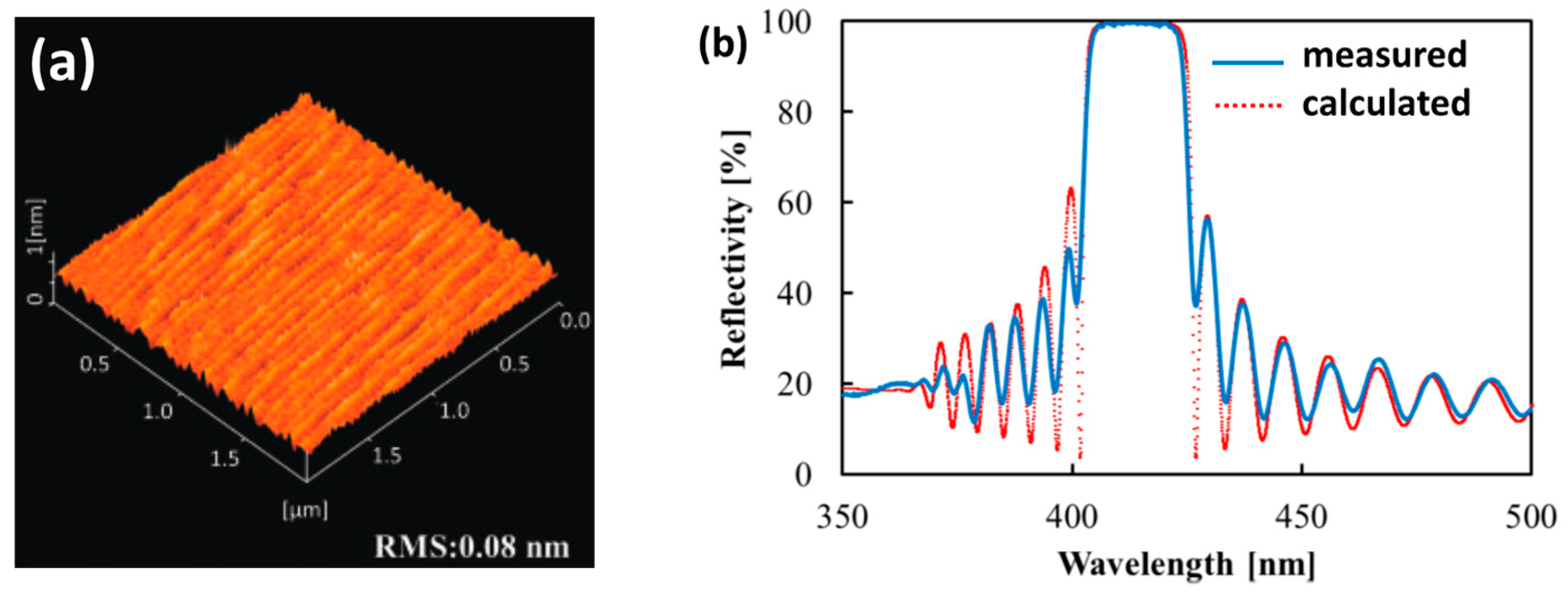
Subsequently, AlInN DBRs were pursued by two groups. Otto-von-Guericke-Universität Magdeburg studied the critical conditions of lattice matching between AlInN and GaN [75]. They also proposed a two-temperature growth procedure [76] and reported the need to use GaN capping layer to improve the interfacial transitions. Meijo University performed very detailed study of OMVPE growth conditions for AlInN and identified a new window for high growth rate (~0.5 μm/h) [77]. The growth condition for a high growth rate requires short gas mixing time, low In/Al ratio and relatively high growth temperature. With such a growth condition, Meijo University demonstrated AlInN/GaN DBRs with more than 99% reflectance in a much-reduced growth time (~12 h) (Figure 7).
In 2016, Meijo University achieved high conductivity in AlInN/GaN DBRs by using modulation doping and composition grading at the GaN/AlInN interfaces [80]. Immediately after the demonstration, they developed VCSELs with conductive AlInN/GaN DBRs with back-side contact, showing the feasibility of GaN-based VCSELs with vertical current injections through conducting DBRs [78]. Since 2017, Stanley Corporation, in collaboration with Meijo University, has further advanced the performance of AlInN-based GaN VCSELs with record high optical power and slope efficiencies [81]. The current trend in AlInN/GaN-based VCSEL structure appears to shift toward longer cavity and non-conductive DBRs [79] toward manufacturing of high-power VCSEL devices for lighting applications. Large-scale commercial manufacturability of VCSEL devices involving AlInN DBRs should become clear in the next few years.
4. Non-Epitaxial DBRs for GaN VCSELs
Since the beginning of GaN VCSEL development, non-epitaxial dielectric DBRs have always been considered as the backup if not the only option. It should be clear from Section 3 that the challenges in nitride epitaxy continues to demand parallel solutions with non-epitaxial DBRs. For the record, Y.K. Song et al. reported in 2000 the first resonant cavity LEDs with two dielectric mirrors [82]. Clear mode patterns and emission directionality was reported even though no threshold behavior was achieved. There are several methods to remove substrates in order to deposit the bottom DBR mirror, which will be reviewed in Section 4.1. Several innovative methods to encase the active region with dielectric DBRs, including epitaxial lateral overgrowth (ELO) and substrate thinning, have produced new and exciting results; they will be discussed in Section 4.2 and Section 4.3, respectively.
4.1. Dielectric DBRs through Substrate Removal
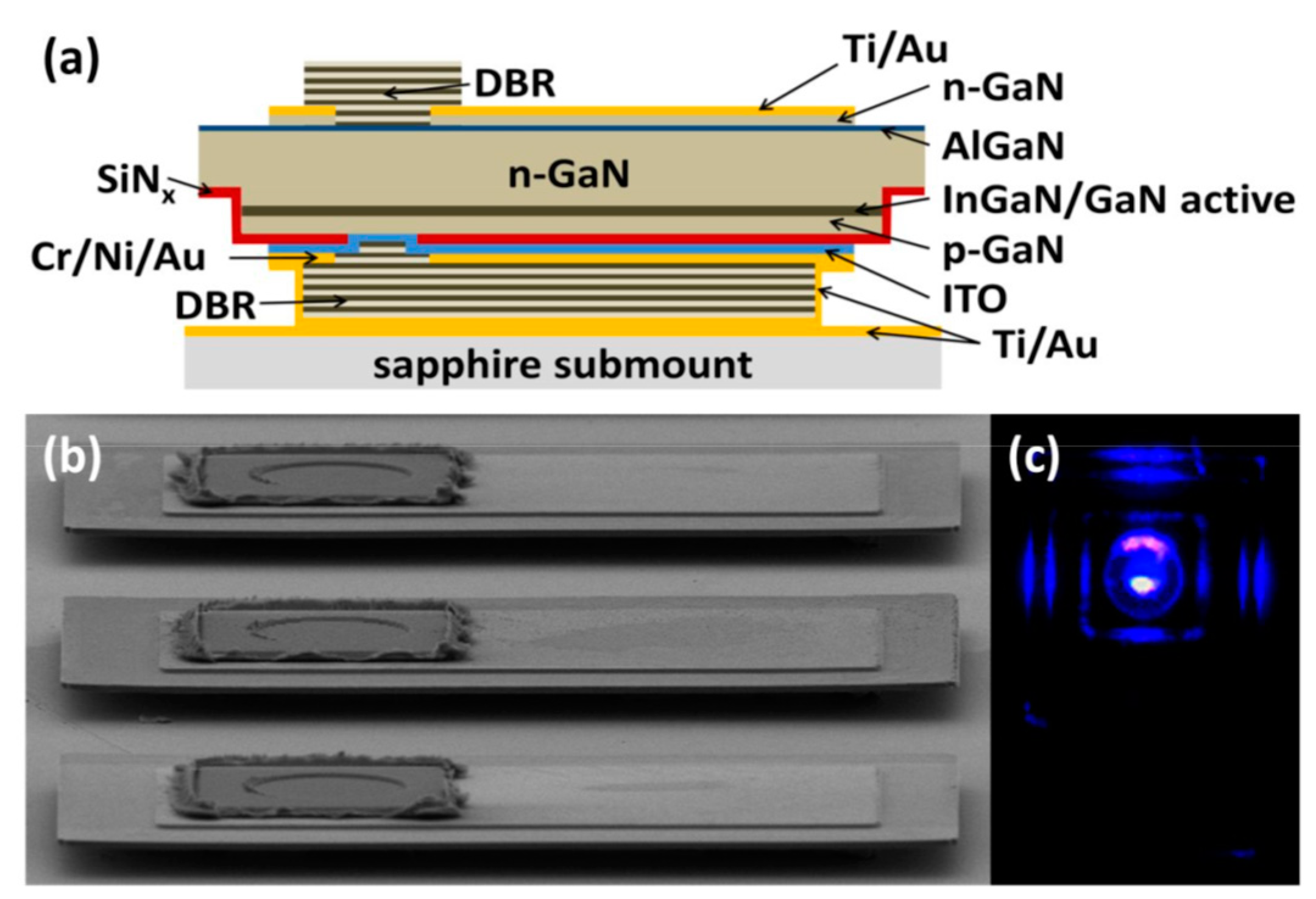
Nichia [20], Panasonic [83], and University of California, Santa Barbara (UCSB) [84], have demonstrated GaN VCSELs using a flip-chip method. In the flip-chip and substrate removal process, a dielectric DBR is firstly deposited on the as-grown surface side (or p-type side), followed by wafer bonding to a handling wafer. Substrate removal can be accomplished by laser-induced liftoff (LLO) [20], photoelectrochemical (PEC) etching of a sacrificial layer [84], wet/dry etching [85], or chemo-mechanical polishing (CMP) [86]. LLO was developed in 1999 [87] to separate GaN LEDs from a sapphire substrate with the back-side irradiation of an excimer laser. This method, however, does not work with GaN or Si substrates due to their opacity to the excimer laser, which is a serious limitation for VCSEL devices grown on bulk GaN substrates. Generally, substrate removal requires a follow-up polishing step to smoothen the surface and fine-tune the cavity thickness after layer separation. Achieving precise control of cavity thickness through polishing, with good uniformity across the entire wafer can be a challenging task. The use of a PEC approach has an advantage of precisely controlling the thickness of the microcavity through a bandgap-selective etching process [84]. A schematic drawing of an all-dielectric VCSEL device using the PEC method is shown in Figure 8. The dielectric DBRs could impede heat dissipation, and UCSB reported a very sophisticated method of heat sinking [88].
4.2. Non-Epitaxial DBRs through Epitaxial Lateral Overgrowth (ELO)
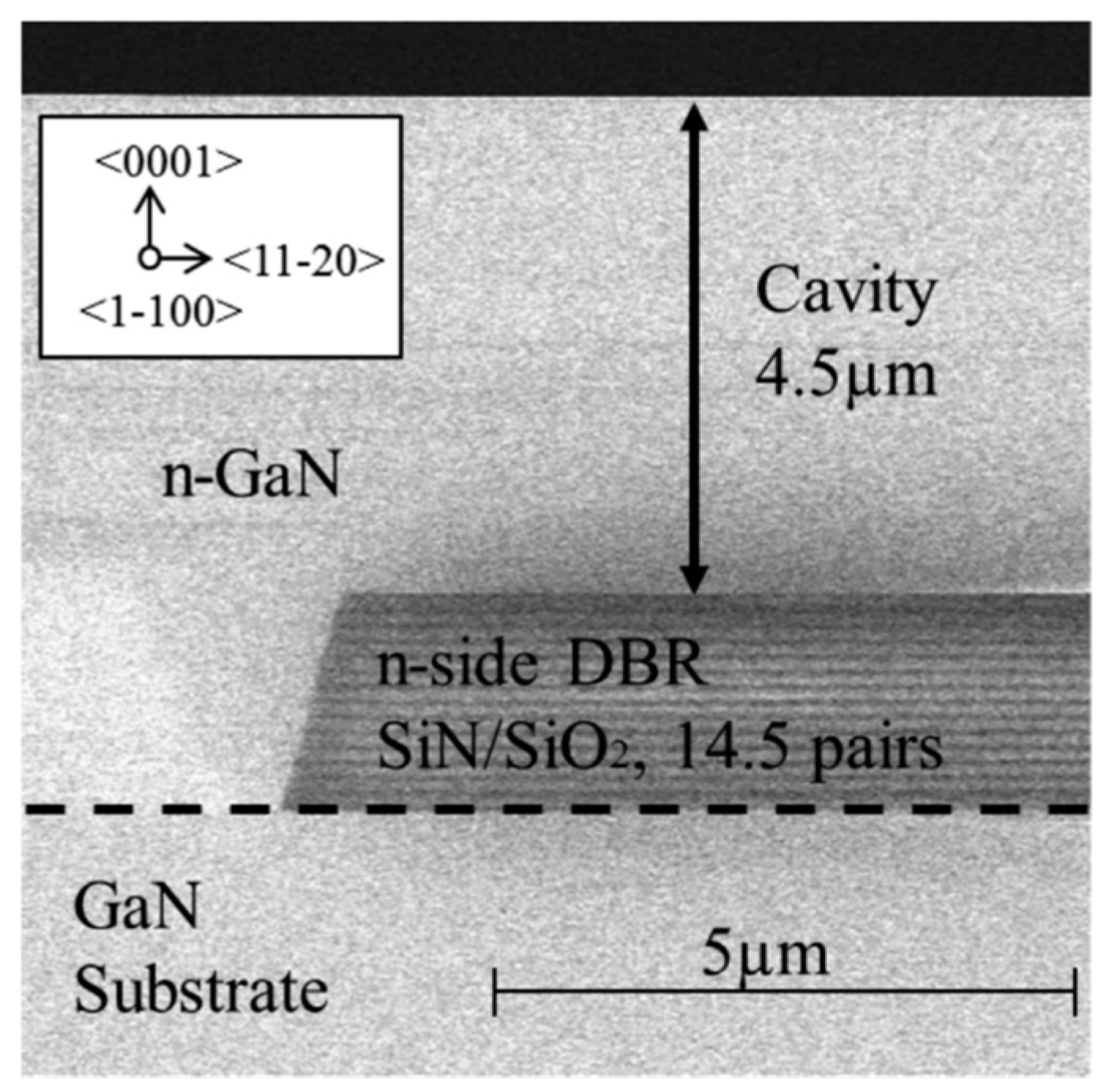
Epitaxial lateral overgrowth (ELO) was a technique used to grow GaN over patterned dielectric mask regions which is effective in dislocation reductions [89]. The idea of utilizing dielectric DBR stacks as ELO mask layers for VCSEL fabrication was first proposed by Nurmikko and Song [90]. Sony Corporation reported in 2015 the use of ELO to fabricate double dielectric VCSELs without substrate removal [54,91]. The fabrication of the VCSEL by the ELO technique starts with a dielectric DBR deposition and patterning on a GaN template. Subsequently, ELO is conducted by MOCVD to grow the remaining VCSEL structure (see Figure 9), and the dielectric DBR is buried by the overgrown GaN layers. Finally, another dielectric DBR is deposited on the top side to form the full microcavity. In spite of the elegance of this approach, there is a practical limitation in the minimum thickness of the microcavity. Given the limited achievable ratio between lateral and vertical growth rates (seldom exceeds 4) in ELO [92], the formation of VCSEL aperture area of greater than 20 or 30 μm for practical fabrication produces correspondingly a cavity of more than 5 or even 10 μm in thickness, thus precluding the possibility of short-cavity, single (longitudinal) mode operation. Another drawback for a long planar VCSEL cavity is an increased diffraction loss, amounting to greater than 1% per round trip for a 10 μm cavity length [54]. Additionally, the uniformity of ELO growth over the entire wafer, for photonic purposes, is still not established and could be a concern.
4.3. Non-Epitaxial DBRs through Substrate Thinning and Curved Dielectric Mirrors
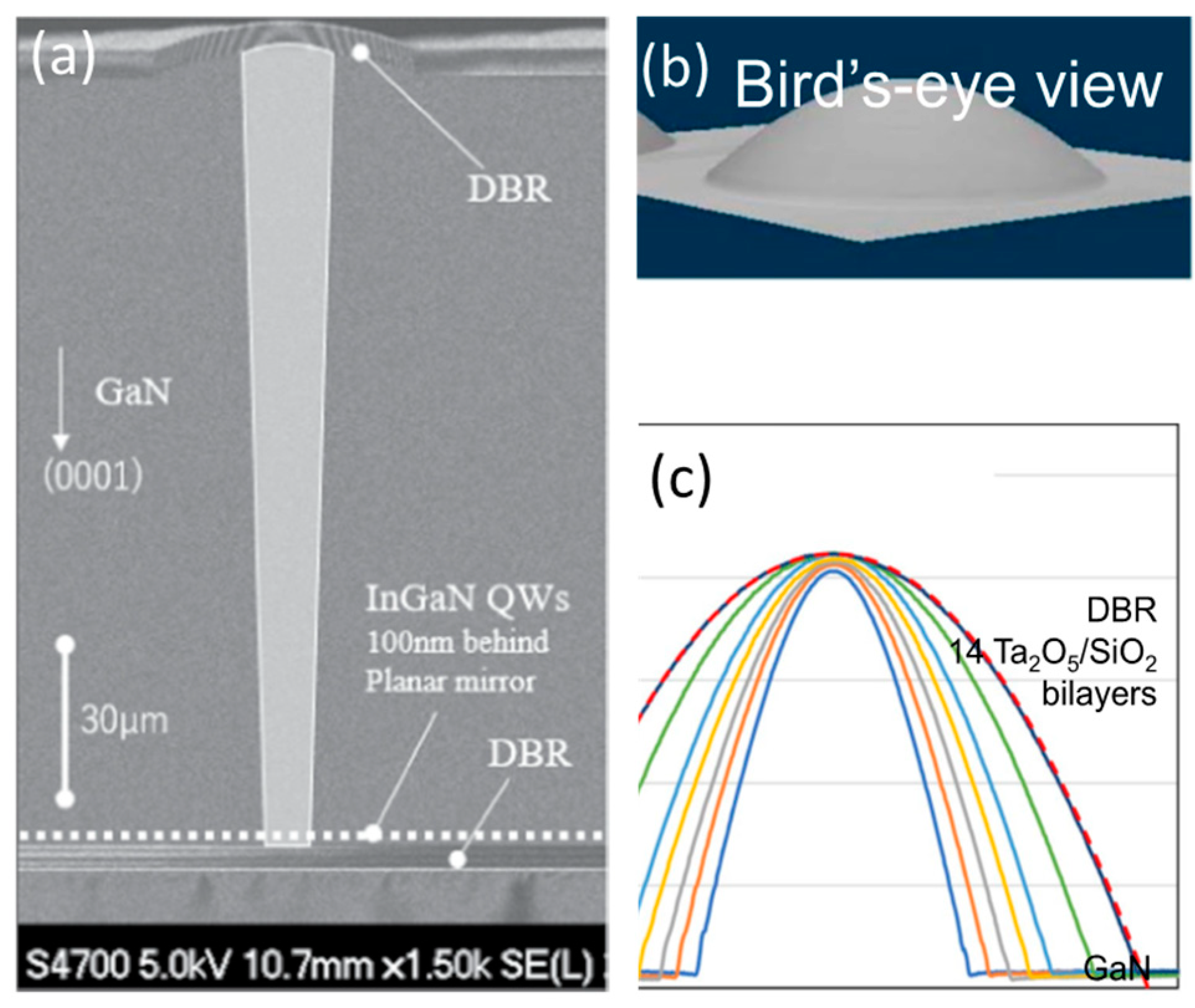
Given the difficulty presented in 4.1 and 4.2 in forming all dielectric mirrors, Sony recently demonstrated yet another version of VCSEL with dielectric mirrors [93] using the concept of “external cavity” where a curved dielectric mirror is coated on the substrate side after substrate thinning [94,95,96]. This implementation, sometimes called thin-disk laser, is possibly the least complicated in terms of both epitaxial growth and device fabrication compared to all other approaches (Figure 10). The use of a very long vertical cavity (>100 λ) is useful for high optical output power [97]. The use of external curved mirrors with controlled curvature offers tunability in engineering the in-plane optical confinement which is typically lacking in III-nitride VCSELs.
5. Airgap and Porous DBRs—A New Approach to Epitaxial DBR
Since air is the ultimate low-index medium, innovative ways have been proposed to create air-containing GaN DBRs from epitaxial GaN structures. The air-containing layers are formed typically by a two-step process, firstly through epitaxy of a “DBR structure”, then followed by selective etching through either chemical, electrochemical, photoelectrochemical, or thermal means. Depending on the embodiment of the low-index layers, the structures can be further divided into GaN/air gap and GaN/nanoporous DBRs.
5.1. GaN/Air Gap DBR
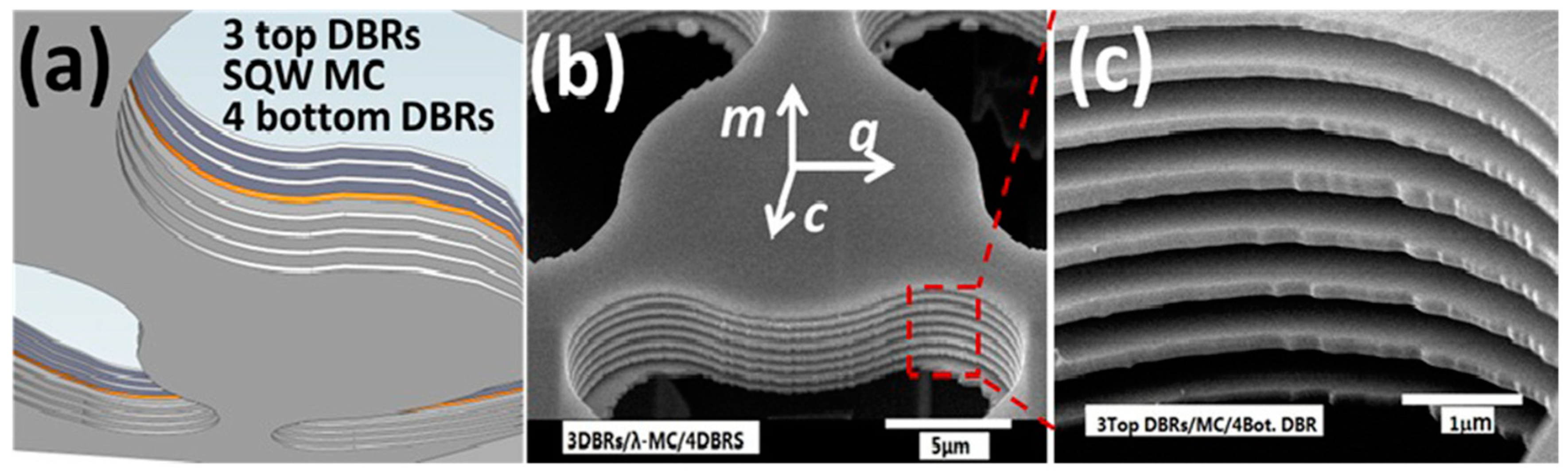
GaN is known to be chemically inert with almost no known wet etchant at room temperature. After the discovery of photoelectrochemical (PEC) etching of GaN [98], this method was employed [99] to create a GaN/air gap DBR where narrow bandgap InGaN layers are used as the sacrificial layer. Microcavity LEDs were also reported using such a GaN/airgap DBR which produces a peak reflectance of around 70% [100]. Several limitations in PEC etching include the structural quality of InGaN sacrificial layers and the available size of the DBR region due to a limited etch rate. Taking advantage of the chemical disparity between GaN and AlInN, several groups [101,102] reported the selective wet-etching of AlInN in an AlInN/GaN structures with hot nitric acid to create GaN/airgap DBRs. Reflectance as high as 99% can be reached with only 4 pairs of DBR. A conductivity-selective electrochemical (EC) etching of GaN was also demonstrated to prepare GaN/airgap DBRs using epitaxially-grown doping superlattices of n+-GaN/GaN structures, followed by selective EC etching [103]. Taking advantage of the large disparity in thermal stability between GaN and AlGaN, Tao et al. reported the selective thermal desorption of GaN in an AlGaN/GaN structure to form AlGaN/airgap DBRs and reported microcavity with a Q-factor of 1600 (Figure 11) [104]. In spite of all the very innovative approaches and the results of broad-band and high-reflectance DBRs, the airgap DBR approach has been confined to optical investigations of cavity physics; challenges in current injection and thermal management have more or less inhibited the possibility of electrical devices.
5.2. Nanoporous GaN/GaN DBRs
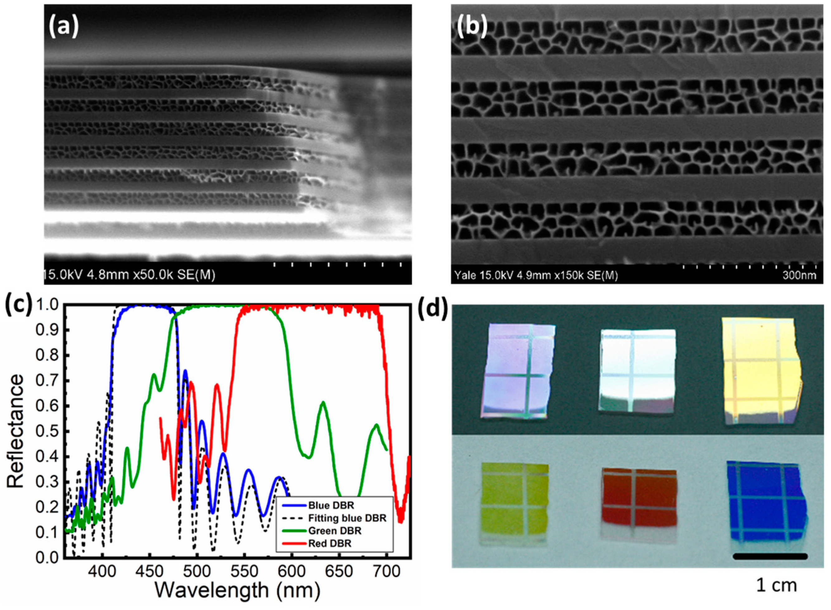
Recently the development of nanoporous (NP) GaN has received much attention. NP GaN can be considered as a nano-composite of perfect single crystalline GaN filled with nanoscale, inter-connected tubes that produce an overall foam or sponge-like texture. A vast amount of literature exists on the formation mechanisms of anodic aluminum oxide [105,106,107], porous silicon [108,109,110,111], and silicon carbide [112,113,114]. The morphology of porous textures and patterns is determined by the highly inhomogeneous etching process, which consists of successive steps including carrier transport in the space-charge (SC) layer, oxidation at the semiconductor surface, transport of ions in the oxide layer (OL), field-enhanced dissolution of oxide at the oxide–electrolyte interface, and ionic transport within the interfacial double layer (DL) [115]. Figure 12a shows a cross-sectional scanning electron microscopy (SEM) image of a porous GaN DBR near the center of the cross-shaped alignment mark. A close-up SEM image of the same structure is shown in Figure 12b with the NP-GaN having a porosity of ~70% and an average pore size of 30 nm. The electrochemistry is highly selective based on the conductivity of and etching bias applied to GaN [116]. The non-porous layer corresponds to lightly n-doped GaN, and the porous layers correspond to n++-GaN before etching. The NP GaN region serves as a low-index medium for the producing of λ/4 reflector. Highly reflective (>99.5%) DBR mirrors in the blue (440 nm), green (520 nm), and red (600 nm) wavelength range have been demonstrated by changing the layer thicknesses (Figure 12c). The epitaxy of n-GaN/n++-GaN structures are straightforward when compared with the challenges in growing Al(GaN) or AlInN DBRs. Nanoporous GaN DBR mirrors with good uniformity are shown under room-light illumination in Figure 12d. Unique advantages of using n-type doping profile to create nanostructured GaN layers include (i) complete lattice matching to conventional GaN structures with negligible degradation in microstructure or morphology, (ii) a high tunability in the index of refractive index, and (iii) the feasibility of electrical injection through n-type NP GaN layers.
Using NP GaN, new freedom is introduced in optical engineering microcavity design without the constraints in epitaxy or complex fabrication. VCSELs with NP GaN based DBR mirrors can be produced with no need for complicated lift-off or flip-chip processes. These properties combined present a unique opportunity to build GaN VCSELs. High-reflectance NP GaN DBR mirrors [117,118,119,120,121,122], optically pumped VCSELs [117,118], and resonant-cavity LEDs (RC-LEDs) [123,124] have been demonstrated by many groups in recently years. The ultimate viability of NP GaN DBRs will be determined by their long-term stability against thermal and electrical stresses. Another common concern with the use of porous medium in semiconductor lasers is the potentially limited thermal conductivity due to a reduced phonon mean free path [125]. Further studies regarding the design tradeoffs between porosity (for index engineering) and the thickness of pore walls [126] for enhanced thermal and electrical transport will be critical. Lastly, during the preparation of this review, an electrically injected VCSEL including NP GaN DBR has also been reported to provide initial validation of this novel concept [127].
6. Concluding Remarks
After more than 20 years of vigorous pursuit, GaN VCSEL research is beginning to transition from laboratory demonstrations to commercial technology. On the one hand, the GaN VCSEL research has been buoyed by the success in LED and LD research. On the other hand, the method to implement vertical cavity for GaN is hardly a settled issue and continues to call for creativity in material and device engineering. At the moment the race, in terms of VCSEL performance and manufacturability, between epitaxial AlInN DBR and the all-dielectric, external cavity design remains a tight one. An alternative approach using nanoporous DBR is offering new flexibility in design and fabrication that may help to ease the rigid constraints and speed up the progress toward commercial GaN VCSELs.
Author Contributions
Conceptualization, C.Z. and J.H.; methodology, C.Z. and J.H; software, C.Z.; validation, C.Z., R.E. and J.H.; formal analysis, C.Z.; investigation, C.Z., R.E. and J.H.; resources, J.H.; data curation, C.Z.; writing—original draft preparation, C.Z.; writing—review and editing, J.H. and R.E.; visualization, C.Z. and J.H.; supervision, J.H.; project administration, J.H.; funding acquisition, J.H.
Funding
This research received no external funding.
Conflicts of Interest
The authors declare no conflict of interest.
References
- Yoshioka, S.; Kinoshita, S. Wavelength–selective and anisotropic light–diffusing scale on the wing of the Morpho butterfly. Proc. R. Soc. Lond. B Biol. Sci. 2004, 271, 581–587. [Google Scholar] [CrossRef]
- Lee, R.T.; Smith, G.S. Detailed electromagnetic simulation for the structural color of butterfly wings. Appl. Opt. 2009, 48, 4177–4190. [Google Scholar] [CrossRef]
- Zi, J.; Yu, X.; Li, Y.; Hu, X.; Xu, C.; Wang, X.; Liu, X.; Fu, R. Coloration strategies in peacock feathers. Proc. Natl. Acad. Sci. USA 2003, 100, 12576–12578. [Google Scholar] [CrossRef] [Green Version]
- Feng, L.; Zhang, Y.; Xi, J.; Zhu, Y.; Wang, N.; Xia, F.; Jiang, L. Petal Effect: A Superhydrophobic State with High Adhesive Force. Langmuir 2008, 24, 4114–4119. [Google Scholar] [CrossRef]
- Yao, H.-B.; Ge, J.; Mao, L.-B.; Yan, Y.-X.; Yu, S.-H. 25th Anniversary Article: Artificial Carbonate Nanocrystals and Layered Structural Nanocomposites Inspired by Nacre: Synthesis, Fabrication and Applications. Adv. Mater. 2014, 26, 163–188. [Google Scholar] [CrossRef]
- De Stefano, L.; Maddalena, P.; Moretti, L.; Rea, I.; Rendina, I.; De Tommasi, E.; Mocella, V.; De Stefano, M. Nano-biosilica from marine diatoms: A brand new material for photonic applications. Superlattices Microstruct. 2009, 46, 84–89. [Google Scholar] [CrossRef]
- Caprio, G.D.; Coppola, G.; Stefano, L.D.; Stefano, M.D.; Antonucci, A.; Congestri, R.; Tommasi, E.D. Shedding light on diatom photonics by means of digital holography. J. Biophotonics 2014, 7, 341–350. [Google Scholar] [CrossRef]
- Vukusic, P.; Sambles, J.R. Corrigendum: Photonic structures in biology. Nature 2004, 429, 680. [Google Scholar] [CrossRef]
- Cartwright, H.; Turner, A.F. Minutes of the Washington, D.C. Meeting, April 27–29, 1939. Phys. Rev. 1939, 55, 1109–1147. [Google Scholar]
- Dimmick, G.L. A New Dichroic Reflector and its Application to Protocell Monitoring Systems. J. Soc. Motion Pict. Eng. 1942, 38, 36–44. [Google Scholar] [CrossRef]
- Banning, M. Practical Methods of Making and Using Multilayer Filters. JOSA 1947, 37, 792–797. [Google Scholar] [CrossRef]
- Ogura, M.; Hata, T.; Kawai, N.J.; Yao, T. GaAs/AlxGa1–xAs Multilayer Reflector for Surface Emitting Laser Diode. Jpn. J. Appl. Phys. 1983, 22, L112. [Google Scholar] [CrossRef]
- Tai, K.; Fischer, R.J.; Seabury, C.W.; Olsson, N.A.; Huo, T.D.; Ota, Y.; Cho, A.Y. Room-temperature continuous-wave vertical-cavity surface-emitting GaAs injection lasers. Appl. Phys. Lett. 1989, 55, 2473–2475. [Google Scholar] [CrossRef]
- Lee, Y.H.; Jewell, J.L.; Scherer, A.; McCall†, S.L.; Harbison, J.P.; Florez, L.T. Room-temperature continuous-wave vertical-cavity single-quantum-well microlaser diodes. Electron. Lett. 1989, 25, 1377–1378. [Google Scholar] [CrossRef] [Green Version]
- Koyama, F. Recent Advances of VCSEL Photonics. J. Light. Technol. 2006, 24, 4502–4513. [Google Scholar] [CrossRef]
- VCSEL Market Worth 3.89 Billion USD by 2023. Available online: https://www.marketsandmarkets.com/PressReleases/vcsel.asp (accessed on 10 March 2019).
- Someya, T.; Werner, R.; Forchel, A.; Catalano, M.; Cingolani, R.; Arakawa, Y. Room Temperature Lasing at Blue Wavelengths in Gallium Nitride Microcavities. Science 1999, 285, 1905–1906. [Google Scholar] [CrossRef]
- Zhou, H.; Diagne, M.; Makarona, E.; Nurmikko, A.V.; Han, J.; Waldrip, K.E.; Figiel, J.J. Near ultraviolet optically pumped vertical cavity laser. Electron. Lett. 2000, 36, 1777–1779. [Google Scholar] [CrossRef]
- Lu, T.-C.; Kao, C.-C.; Kuo, H.-C.; Huang, G.-S.; Wang, S.-C. CW lasing of current injection blue GaN-based vertical cavity surface emitting laser. Appl. Phys. Lett. 2008, 92, 141102. [Google Scholar] [CrossRef]
- Higuchi, Y.; Omae, K.; Matsumura, H.; Mukai, T. Room-Temperature CW Lasing of a GaN-Based Vertical-Cavity Surface-Emitting Laser by Current Injection. Appl. Phys. Express 2008, 1, 121102. [Google Scholar] [CrossRef]
- Perry, D.L. Low-Loss Multilayer Dielectric Mirrors. Appl. Opt. 1965, 4, 987–991. [Google Scholar] [CrossRef]
- Baumeister, P. Optical Coating Technology; SPIE Press: Bellingham, WA, USA, 2004; ISBN 978-0-8194-5313-6. [Google Scholar]
- Iga, K.; Koyama, F.; Kinoshita, S. Surface emitting semiconductor lasers. IEEE J. Quantum Electron. 1988, 24, 1845–1855. [Google Scholar] [CrossRef]
- Soda, H.; Iga, K.; Kitahara, C.; Suematsu, Y. GaInAsP/InP Surface Emitting Injection Lasers. Jpn. J. Appl. Phys. 1979, 18, 2329. [Google Scholar] [CrossRef]
- Soda, H.; Motegi, Y.; Iga, K. GaInAsP/InP surface emitting injection lasers with short cavity length. IEEE J. Quantum Electron. 1983, 19, 1035–1041. [Google Scholar] [CrossRef]
- Iga, K.; Ishikawa, S.; Ohkouchi, S.; Nishimura, T. Room temperature pulsed oscillation of GaAlAs/GaAs surface emitting junction laser. IEEE J. Quantum Electron. 1985, 21, 663–668. [Google Scholar] [CrossRef]
- Iga, K.; Kinoshita, S.; Koyama, F. Microcavity GalaAs/GaAs surface-emitting laser with Ith = 6 mA. Electron. Lett. 1987, 23, 134–136. [Google Scholar] [CrossRef]
- Koyama, F.; Uenohara, H.; Sakaguchi, T.; Iga, K. GaAlAs/GaAs MOCVD Growth for Surface Emitting Laser. Jpn. J. Appl. Phys. 1987, 26, 1077. [Google Scholar] [CrossRef]
- Singh, J.; Bajaj, K.K. Theoretical investigations of the nature of the normal and inverted GaAs–AlGaAs structures grown by molecular beam epitaxy. J. Vac. Sci. Technol. B Microelectron. Process. Phenom. 1984, 2, 576–581. [Google Scholar] [CrossRef]
- Sakaki, H.; Noda, T.; Hirakawa, K.; Tanaka, M.; Matsusue, T. Interface roughness scattering in GaAs/AlAs quantum wells. Appl. Phys. Lett. 1987, 51, 1934–1936. [Google Scholar] [CrossRef]
- Sakaki, H.; Tanaka, M.; Yoshino, J. One Atomic Layer Heterointerface Fluctuations in GaAs-AlAs Quantum Well Structures and Their Suppression by Insertion of Smoothing Period in Molecular Beam Epitaxy. Jpn. J. Appl. Phys. 1985, 24, L417. [Google Scholar] [CrossRef]
- Egorov, A.Y.; Kovsh, A.R.; Ustinov, V.M.; Zhukov, A.E.; Kop’ev, P.S.; Tu, C.W. A thermodynamic analysis of the growth of III–V compounds with two volatile group V elements by molecular-beam epitaxy. J. Cryst. Growth 1998, 188, 69–74. [Google Scholar] [CrossRef]
- Liang, B.W.; Tu, C.W. A kinetic model for As and P incorporation behaviors in GaAsP grown by gas-source molecular beam epitaxy. J. Appl. Phys. 1993, 74, 255–259. [Google Scholar] [CrossRef]
- Johnson, K.; Hibbs-Brenner, M.; Hogan, W.; Dummer, M.; Dogubo, K.; Berg, G. Record high temperature high output power red VCSELs. SPIE 2011, 7952, 795208. [Google Scholar]
- Westphalen, R.; Landgren, G.; Stalnacke, B.; Beccard, R. Improved homogeneity of LP-MOVPE grown InP/GaInAsP heterostructure for DBR using an optimized liner and susceptor arrangement. In Proceedings of the Eleventh International Conference on Indium Phosphide and Related Materials (IPRM’99) (Cat. No. 99CH36362), Davos, Switzerland, 16–20 May 1999; pp. 139–142. [Google Scholar]
- Hou, H.Q.; Chui, H.C.; Choquette, K.D.; Hammons, B.E.; Breiland, W.G.; Geib, K.M. Highly uniform and reproducible vertical-cavity surface-emitting lasers grown by metalorganic vapor phase epitaxy with in situ reflectometry. IEEE Photonics Technol. Lett. 1996, 8, 1285–1287. [Google Scholar] [CrossRef]
- Asom, M.T.; Geva, M.; Leibenguth, R.E.; Chu, S.N.G. Interface disorder in AlAs/(Al)GaAs Bragg reflectors. Appl. Phys. Lett. 1991, 59, 976–978. [Google Scholar] [CrossRef]
- Zhang, Z.; von Würtemberg, R.M.; Berggren, J.; Hammar, M. Optical loss and interface morphology in AlGaAs/GaAs distributed Bragg reflectors. Appl. Phys. Lett. 2007, 91, 101101. [Google Scholar] [CrossRef]
- Schneider, R.P.; Lott, J.A. InAIP/InAlGaP distributed Bragg reflectors for visible vertical cavity surface-emitting lasers. Appl. Phys. Lett. 1993, 62, 2748–2750. [Google Scholar] [CrossRef]
- Tuttle, G.; Kavanaugh, J.; McCalmont, S. (Al,Ga)Sb long-wavelength distributed Bragg reflectors. IEEE Photonics Technol. Lett. 1993, 5, 1376–1379. [Google Scholar] [CrossRef]
- Duan, X.; Huang, Y.; Shang, Y.; Wang, J.; Ren, X. High-efficiency dual-absorption InGaAs/InP photodetector incorporating GaAs/AlGaAs Bragg reflectors. Opt. Lett. 2014, 39, 2447–2450. [Google Scholar] [CrossRef]
- Vučković, J.; Pelton, M.; Scherer, A.; Yamamoto, Y. Optimization of three-dimensional micropost microcavities for cavity quantum electrodynamics. Phys. Rev. A 2002, 66, 023808. [Google Scholar] [CrossRef]
- Coldren, L.A.; Corzine, S.W.; Mashanovitch, M.L. Diode Lasers and Photonic Integrated Circuits, 2nd ed.; Wiley: Hoboken, NJ, USA, 2012; Available online: https://0-www-wiley-com.brum.beds.ac.uk/en-us/Diode+Lasers+and+Photonic+Integrated+Circuits%2C+2nd+Edition-p-9780470484128 (accessed on 19 February 2019).
- Carlin, J.-F.; Ilegems, M. High-quality AlInN for high index contrast Bragg mirrors lattice matched to GaN. Appl. Phys. Lett. 2003, 83, 668–670. [Google Scholar] [CrossRef]
- Wilmsen, C.W.; Coldren, L.A.; Temkin, H. Vertical-Cavity Surface-Emitting Lasers: Design, Fabrication, Characterization, and Applications; Cambridge University Press: Cambridge, UK, 2001; ISBN 978-0-521-00629-3. [Google Scholar]
- Mishkat-Ul-Masabih, S.; Leonard, J.; Cohen, D.; Nakamura, S.; Feezell, D. Techniques to reduce thermal resistance in flip-chip GaN-based VCSELs. Phys. Status Solidi A 2017, 214, 1600819. [Google Scholar] [CrossRef]
- Mei, Y.; Xu, R.-B.; Xu, H.; Ying, L.-Y.; Zheng, Z.-W.; Zhang, B.-P.; Li, M.; Zhang, J. A comparative study of thermal characteristics of GaN-based VCSELs with three different typical structures. Semicond. Sci. Technol. 2017, 33, 015016. [Google Scholar] [CrossRef] [Green Version]
- Forman, C.A.; Lee, S.; Young, E.C.; Kearns, J.A.; Cohen, D.A.; Leonard, J.T.; Margalith, T.; DenBaars, S.P.; Nakamura, S. Continuous-wave operation of nonpolar GaN-based vertical-cavity surface-emitting lasers. SPIE 2018, 10532, 105321C. [Google Scholar]
- Zhou, P.; Cheng, J.; Schaus, C.F.; Sun, S.Z.; Zheng, K.; Armour, E.; Hains, C.; Hsin, W.; Myers, D.R.; Vawter, G.A. Low series resistance high-efficiency GaAs/AlGaAs vertical-cavity surface-emitting lasers with continuously graded mirrors grown by MOCVD. IEEE Photonics Technol. Lett. 1991, 3, 591–593. [Google Scholar] [CrossRef]
- Piprek, J.; Troger, T.; Schroter, B.; Kolodzey, J.; Ih, C.S. Thermal conductivity reduction in GaAs-AlAs distributed Bragg reflectors. IEEE Photonics Technol. Lett. 1998, 10, 81–83. [Google Scholar] [CrossRef]
- Sugimoto, M.; Kosaka, H.; Kurihara, K.; Ogura, I.; Numai, T.; Kasahara, K. Very low threshold current density in vertical-cavity surface-emitting laser diodes with periodically doped distributed Bragg reflectors. Electron. Lett. 1992, 28, 385–387. [Google Scholar] [CrossRef]
- Lear, K.L.; Schneider, R.P. Uniparabolic mirror grading for vertical cavity surface emitting lasers. Appl. Phys. Lett. 1996, 68, 605–607. [Google Scholar] [CrossRef] [Green Version]
- Chalmers, S.A.; Lear, K.L.; Killeen, K.P. Low resistance wavelength-reproducible p-type (Al,Ga)As distributed Bragg reflectors grown by molecular beam epitaxy. Appl. Phys. Lett. 1993, 62, 1585–1587. [Google Scholar] [CrossRef]
- Hamaguchi, T.; Fuutagawa, N.; Izumi, S.; Murayama, M.; Narui, H. Milliwatt-class GaN-based blue vertical-cavity surface-emitting lasers fabricated by epitaxial lateral overgrowth. Phys. Status Solidi A 2016, 213, 1170–1176. [Google Scholar] [CrossRef]
- Gherasimova, M.; Cui, G.; Ren, Z.; Su, J.; Wang, X.-L.; Han, J.; Higashimine, K.; Otsuka, N. Heteroepitaxial evolution of AlN on GaN Grown by metal-organic chemical vapor deposition. J. Appl. Phys. 2004, 95, 2921–2923. [Google Scholar] [CrossRef]
- Pastrňák, J.; Roskovcová, L. Refraction Index Measurements on AlN Single Crystals. Phys. Status Solidi B 1966, 14, K5–K8. [Google Scholar] [CrossRef]
- Barker, A.S.; Ilegems, M. Infrared Lattice Vibrations and Free-Electron Dispersion in GaN. Phys. Rev. B 1973, 7, 743–750. [Google Scholar] [CrossRef]
- Khan, M.A.; Kuznia, J.N.; Van Hove, J.M.; Olson, D.T. Reflective filters based on single-crystal GaN/AlxGa1−xN multilayers deposited using low-pressure metalorganic chemical vapor deposition. Appl. Phys. Lett. 1991, 59, 1449–1451. [Google Scholar] [CrossRef]
- Redwing, J.M.; Loeber, D.A.S.; Anderson, N.G.; Tischler, M.A.; Flynn, J.S. An optically pumped GaN–AlGaN vertical cavity surface emitting laser. Appl. Phys. Lett. 1996, 69, 1–3. [Google Scholar] [CrossRef]
- Nakada, N.; Ishikawa, H.; Egawa, T.; Jimbo, T. Suppression of Crack Generation in GaN/AlGaN Distributed Bragg Reflector on Sapphire by the Insertion of GaN/AlGaN Superlattice Grown by Metal-Organic Chemical Vapor Deposition. Jpn. J. Appl. Phys. 2003, 42, L144. [Google Scholar] [CrossRef]
- Han, J.; Waldrip, K.E.; Lee, S.R.; Figiel, J.J.; Hearne, S.J.; Petersen, G.A.; Myers, S.M. Control and elimination of cracking of AlGaN using low-temperature AlGaN interlayers. Appl. Phys. Lett. 2000, 78, 67–69. [Google Scholar] [CrossRef]
- Krestnikov, I.L.; Lundin, W.V.; Sakharov, A.V.; Semenov, V.A.; Usikov, A.S.; Tsatsul’nikov, A.F.; Alferov, Z.I.; Ledentsov, N.N.; Hoffmann, A.; Bimberg, D. Room-temperature photopumped InGaN/GaN/AlGaN vertical-cavity surface-emitting laser. Appl. Phys. Lett. 1999, 75, 1192–1194. [Google Scholar] [CrossRef]
- Nakada, N.; Ishikawa, H.; Egawa, T.; Jimbo, T.; Umeno, M. MOCVD growth of high reflective GaN/AlGaN distributed Bragg reflectors. J. Cryst. Growth 2002, 237–239, 961–967. [Google Scholar] [CrossRef]
- Bhattacharyya, A.; Iyer, S.; Iliopoulos, E.; Sampath, A.V.; Cabalu, J.; Moustakas, T.D.; Friel, I. High reflectivity and crack-free AlGaN/AlN ultraviolet distributed Bragg reflectors. J. Vac. Sci. Technol. B Microelectron. Nanometer Struct. Process. Meas. Phenom. 2002, 20, 1229–1233. [Google Scholar] [CrossRef]
- Natali, F.; Byrne, D.; Dussaigne, A.; Grandjean, N.; Massies, J.; Damilano, B. High-Al-content crack-free AlGaN/GaN Bragg mirrors grown by molecular-beam epitaxy. Appl. Phys. Lett. 2003, 82, 499–501. [Google Scholar] [CrossRef]
- Mitrofanov, O.; Schmult, S.; Manfra, M.J.; Siegrist, T.; Weimann, N.G.; Sergent, A.M.; Molnar, R.J. High-reflectivity ultraviolet AlGaN/AlGaN distributed Bragg reflectors. Appl. Phys. Lett. 2006, 88, 171101. [Google Scholar] [CrossRef]
- Kao, C.-C.; Peng, Y.C.; Yao, H.H.; Tsai, J.Y.; Chang, Y.H.; Chu, J.T.; Huang, H.W.; Kao, T.T.; Lu, T.C.; Kuo, H.C.; et al. Fabrication and performance of blue GaN-based vertical-cavity surface emitting laser employing AlN/GaN and Ta2O5/SiO2 distributed Bragg reflector. Appl. Phys. Lett. 2005, 87, 081105. [Google Scholar] [CrossRef]
- Diagne, M.; He, Y.; Zhou, H.; Makarona, E.; Nurmikko, A.V.; Han, J.; Waldrip, K.E.; Figiel, J.J.; Takeuchi, T.; Krames, M. Vertical cavity violet light emitting diode incorporating an aluminum gallium nitride distributed Bragg mirror and a tunnel junction. Appl. Phys. Lett. 2001, 79, 3720–3722. [Google Scholar] [CrossRef]
- Li, Z.-Y.; Lu, T.-C.; Kuo, H.-C.; Wang, S.-C.; Lo, M.-H.; Lau, K.M. HRTEM investigation of high-reflectance AlN/GaN distributed Bragg-reflectors by inserting AlN/GaN superlattice. J. Cryst. Growth 2009, 311, 3089–3092. [Google Scholar] [CrossRef]
- Kim, K.S.; Saxler, A.; Kung, P.; Razeghi, M.; Lim, K.Y. Determination of the band-gap energy of Al1−xInxN grown by metal–organic chemical-vapor deposition. Appl. Phys. Lett. 1997, 71, 800–802. [Google Scholar] [CrossRef]
- Han, J.; Figiel, J.J.; Petersen, G.A.; Myers, S.M.; Crawford, M.H.; Banas, M.A. Metal-Organic Vapor-Phase Epitaxial Growth and Characterization of Quaternary AlGaInN. Jpn. J. Appl. Phys. 2000, 39, 2372. [Google Scholar] [CrossRef]
- Butté, R.; Carlin, J.-F.; Feltin, E.; Gonschorek, M.; Nicolay, S.; Christmann, G.; Simeonov, D.; Castiglia, A.; Dorsaz, J.; Buehlmann, H.J.; et al. Current status of AlInN layers lattice-matched to GaN for photonics and electronics. J. Phys. Appl. Phys. 2007, 40, 6328–6344. [Google Scholar] [CrossRef]
- Carlin, J.-F.; Dorsaz, J.; Feltin, E.; Butté, R.; Grandjean, N.; Ilegems, M.; Laügt, M. Crack-free fully epitaxial nitride microcavity using highly reflective AlInN/GaN Bragg mirrors. Appl. Phys. Lett. 2005, 86, 031107. [Google Scholar] [CrossRef]
- Cosendey, G.; Castiglia, A.; Rossbach, G.; Carlin, J.-F.; Grandjean, N. Blue monolithic AlInN-based vertical cavity surface emitting laser diode on free-standing GaN substrate. Appl. Phys. Lett. 2012, 101, 151113. [Google Scholar] [CrossRef]
- Krost, A.; Berger, C.; Bläsing, J.; Franke, A.; Hempel, T.; Dadgar, A.; Christen, J. Strain evaluation in AlInN/GaN Bragg mirrors by in situ curvature measurements and ex situ x-ray grazing incidence and transmission scattering. Appl. Phys. Lett. 2010, 97, 181105. [Google Scholar] [CrossRef]
- Berger, C.; Dadgar, A.; Bläsing, J.; Lesnik, A.; Veit, P.; Schmidt, G.; Hempel, T.; Christen, J.; Krost, A.; Strittmatter, A. Growth of AlInN/GaN distributed Bragg reflectors with improved interface quality. J. Cryst. Growth 2015, 414, 105–109. [Google Scholar] [CrossRef]
- Kozuka, Y.; Ikeyama, K.; Yasuda, T.; Takeuchi, T.; Kamiyama, S.; Iwaya, M.; Akasaki, I. Growths of AlInN Single Layers and Distributed Bragg Reflectors for VCSELs. MRS Online Proc. Libr. Arch. 2015, 1736. [Google Scholar] [CrossRef]
- Ikeyama, K.; Kozuka, Y.; Matsui, K.; Yoshida, S.; Akagi, T.; Akatsuka, Y.; Koide, N.; Takeuchi, T.; Kamiyama, S.; Iwaya, M.; et al. Room-temperature continuous-wave operation of GaN-based vertical-cavity surface-emitting lasers with n-type conducting AlInN/GaN distributed Bragg reflectors. Appl. Phys. Express 2016, 9, 102101. [Google Scholar] [CrossRef] [Green Version]
- Takeuchi, T.; Kamiyama, S.; Iwaya, M.; Akasaki, I. GaN-based vertical-cavity surface-emitting lasers with AlInN/GaN distributed Bragg reflectors. Rep. Prog. Phys. 2018, 82, 012502. [Google Scholar] [CrossRef]
- Yoshida, S.; Ikeyama, K.; Yasuda, T.; Furuta, T.; Takeuchi, T.; Iwaya, M.; Kamiyama, S.; Akasaki, I. Electron and hole accumulations at GaN/AlInN/GaN interfaces and conductive n-type AlInN/GaN distributed Bragg reflectors. Jpn. J. Appl. Phys. 2016, 55, 05FD10. [Google Scholar] [CrossRef]
- Kuramoto, M.; Kobayashi, S.; Akagi, T.; Tazawa, K.; Tanaka, K.; Saito, T.; Takeuchi, T. Enhancement of slope efficiency and output power in GaN-based vertical-cavity surface-emitting lasers with a SiO2-buried lateral index guide. Appl. Phys. Lett. 2018, 112, 111104. [Google Scholar] [CrossRef]
- Song, Y.-K.; Diagne, M.; Zhou, H.; Nurmikko, A.V.; Schneider, R.P.; Takeuchi, T. Resonant-cavity InGaN quantum-well blue light-emitting diodes. Appl. Phys. Lett. 2000, 77, 1744–1746. [Google Scholar] [CrossRef]
- Onishi, T.; Imafuji, O.; Nagamatsu, K.; Kawaguchi, M.; Yamanaka, K.; Takigawa, S. Continuous Wave Operation of GaN Vertical Cavity Surface Emitting Lasers at Room Temperature. IEEE J. Quantum Electron. 2012, 48, 1107–1112. [Google Scholar] [CrossRef]
- Holder, C.; Speck, J.S.; DenBaars, S.P.; Nakamura, S.; Feezell, D. Demonstration of Nonpolar GaN-Based Vertical-Cavity Surface-Emitting Lasers. Appl. Phys. Express 2012, 5, 092104. [Google Scholar] [CrossRef]
- Cai, W.; Yuan, J.; Ni, S.; Shi, Z.; Zhou, W.; Liu, Y.; Wang, Y.; Amano, H. GaN-on-Si resonant-cavity light-emitting diode incorporating top and bottom dielectric distributed Bragg reflectors. Appl. Phys. Express 2019, 12, 032004. [Google Scholar] [CrossRef]
- Kasahara, D.; Morita, D.; Kosugi, T.; Nakagawa, K.; Kawamata, J.; Higuchi, Y.; Matsumura, H.; Mukai, T. Demonstration of Blue and Green GaN-Based Vertical-Cavity Surface-Emitting Lasers by Current Injection at Room Temperature. Appl. Phys. Express 2011, 4, 072103. [Google Scholar] [CrossRef]
- Wong, W.S.; Sands, T.; Cheung, N.W.; Kneissl, M.; Bour, D.P.; Mei, P.; Romano, L.T.; Johnson, N.M. Fabrication of thin-film InGaN light-emitting diode membranes by laser lift-off. Appl. Phys. Lett. 1999, 75, 1360–1362. [Google Scholar] [CrossRef]
- Leonard, J.T.; Cohen, D.A.; Yonkee, B.P.; Farrell, R.M.; Margalith, T.; Lee, S.; DenBaars, S.P.; Speck, J.S.; Nakamura, S. Nonpolar III-nitride vertical-cavity surface-emitting lasers incorporating an ion implanted aperture. Appl. Phys. Lett. 2015, 107, 011102. [Google Scholar] [CrossRef]
- Nam, O.-H.; Bremser, M.D.; Zheleva, T.S.; Davis, R.F. Lateral epitaxy of low defect density GaN layers via organometallic vapor phase epitaxy. Appl. Phys. Lett. 1997, 71, 2638–2640. [Google Scholar] [CrossRef]
- Nurmikko, A.V.; Song, Y.-K. Blue/Ultraviolet/Green Vertical Cavity Surface Emitting Laser Employing Lateral Edge Overgrowth (LEO) technique. U.S. Patent 6233267B1, 15 May 2001. [Google Scholar]
- Izumi, S.; Fuutagawa, N.; Hamaguchi, T.; Murayama, M.; Kuramoto, M.; Narui, H. Room-temperature continuous-wave operation of GaN-based vertical-cavity surface-emitting lasers fabricated using epitaxial lateral overgrowth. Appl. Phys. Express 2015, 8, 062702. [Google Scholar] [CrossRef]
- Kapolnek, D.; Keller, S.; Vetury, R.; Underwood, R.D.; Kozodoy, P.; Den Baars, S.P.; Mishra, U.K. Anisotropic epitaxial lateral growth in GaN selective area epitaxy. Appl. Phys. Lett. 1997, 71, 1204–1206. [Google Scholar] [CrossRef]
- Hamaguchi, T.; Tanaka, M.; Mitomo, J.; Nakajima, H.; Ito, M.; Ohara, M.; Kobayashi, N.; Fujii, K.; Watanabe, H.; Satou, S.; et al. Lateral optical confinement of GaN-based VCSEL using an atomically smooth monolithic curved mirror. Sci. Rep. 2018, 8, 10350. [Google Scholar] [CrossRef] [PubMed]
- Park, S.-H.; Kim, J.; Jeon, H.; Sakong, T.; Lee, S.-N.; Chae, S.; Park, Y.; Jeong, C.-H.; Yeom, G.-Y.; Cho, Y.-H. Room-temperature GaN vertical-cavity surface-emitting laser operation in an extended cavity scheme. Appl. Phys. Lett. 2003, 83, 2121–2123. [Google Scholar] [CrossRef]
- Debusmann, R.; Dhidah, N.; Hoffmann, V.; Weixelbaum, L.; Brauch, U.; Graf, T.; Weyers, M.; Kneissl, M. InGaN–GaN Disk Laser for Blue-Violet Emission Wavelengths. IEEE Photonics Technol. Lett. 2010, 22, 652–654. [Google Scholar] [CrossRef]
- Wunderer, T.; Northrup, J.E.; Yang, Z.; Teepe, M.; Strittmatter, A.; Johnson, N.M.; Rotella, P.; Wraback, M. In-well pumping of InGaN/GaN vertical-external-cavity surface-emitting lasers. Appl. Phys. Lett. 2011, 99, 201109. [Google Scholar] [CrossRef]
- Mende, J.; Spindler, G.; Speiser, J.; Giesen, A. Concept of neutral gain modules for power scaling of thin-disk lasers. Appl. Phys. B 2009, 97, 307. [Google Scholar] [CrossRef]
- Hu, E.L.; Minsky, M.S. Photoelectrochemical Wet Etching of Group III Nitrides. U.S. Patent 5773369A, 30 June 1998. [Google Scholar]
- Sharma, R.; Haberer, E.D.; Meier, C.; Hu, E.L.; Nakamura, S. Vertically oriented GaN-based air-gap distributed Bragg reflector structure fabricated using band-gap-selective photoelectrochemical etching. Appl. Phys. Lett. 2005, 87, 051107. [Google Scholar] [CrossRef]
- Sharma, R.; Choi, Y.-S.; Wang, C.-F.; David, A.; Weisbuch, C.; Nakamura, S.; Hu, E.L. Gallium-nitride-based microcavity light-emitting diodes with air-gap distributed Bragg reflectors. Appl. Phys. Lett. 2007, 91, 211108. [Google Scholar] [CrossRef]
- Bellanger, M.; Bousquet, V.; Christmann, G.; Baumberg, J.; Kauer, M. Highly Reflective GaN-Based Air-Gap Distributed Bragg Reflectors Fabricated Using AlInN Wet Etching. Appl. Phys. Express 2009, 2, 121003. [Google Scholar] [CrossRef]
- Xiong, C.; Edwards, P.R.; Christmann, G.; Gu, E.; Dawson, M.D.; Baumberg, J.J.; Martin, R.W.; Watson, I.M. High-reflectivity GaN/air vertical distributed Bragg reflectors fabricated by wet etching of sacrificial AlInN layers. Semicond. Sci. Technol. 2010, 25, 032001. [Google Scholar] [CrossRef] [Green Version]
- Chen, D.; Han, J. High reflectance membrane-based distributed Bragg reflectors for GaN photonics. Appl. Phys. Lett. 2012, 101, 221104. [Google Scholar] [CrossRef]
- Tao, R.; Arita, M.; Kako, S.; Arakawa, Y. Fabrication and optical properties of non-polar III-nitride air-gap distributed Bragg reflector microcavities. Appl. Phys. Lett. 2013, 103, 201118. [Google Scholar] [CrossRef]
- Thompson, G.E.; Wood, G.C. Porous anodic film formation on aluminium. Nature 1981, 290, 230. [Google Scholar] [CrossRef]
- Parkhutik, V.P.; Shershulsky, V.I. Theoretical modelling of porous oxide growth on aluminium. J. Phys. Appl. Phys. 1992, 25, 1258–1263. [Google Scholar] [CrossRef]
- Jessensky, O.; Müller, F.; Gösele, U. Self-organized formation of hexagonal pore arrays in anodic alumina. Appl. Phys. Lett. 1998, 72, 1173–1175. [Google Scholar] [CrossRef]
- Beale, M.I.J.; Benjamin, J.D.; Uren, M.J.; Chew, N.G.; Cullis, A.G. An experimental and theoretical study of the formation and microstructure of porous silicon. J. Cryst. Growth 1985, 73, 622–636. [Google Scholar] [CrossRef]
- Smith, R.L.; Collins, S.D. Porous silicon formation mechanisms. J. Appl. Phys. 1992, 71, R1–R22. [Google Scholar] [CrossRef]
- Zhang, X.G. Morphology and Formation Mechanisms of Porous Silicon. J. Electrochem. Soc. 2004, 151, C69–C80. [Google Scholar] [CrossRef]
- Hasse, G.; Christophersen, M.; Carstensen, J.; Föll, H. New Insights into Si Electrochemistry and Pore Growth by Transient Measurements and Impedance Spectroscopy. Phys. Status Solidi A 2000, 182, 23–29. [Google Scholar] [CrossRef]
- Konstantinov, A.O.; Harris, C.I.; Janzén, E. Electrical properties and formation mechanism of porous silicon carbide. Appl. Phys. Lett. 1994, 65, 2699–2701. [Google Scholar] [CrossRef]
- Ke, Y.; Devaty, R.P.; Choyke, W.J. Self-Ordered Nanocolumnar Pore Formation in the Photoelectrochemical Etching of 6H SiC. Electrochem. Solid-State Lett. 2007, 10, K24–K27. [Google Scholar] [CrossRef]
- Ke, Y.; Devaty, R.P.; Choyke, W.J. Comparative columnar porous etching studies on n-type 6H SiC crystalline faces. Phys. Status Solidi B 2008, 245, 1396–1403. [Google Scholar] [CrossRef]
- Chen, D.; Xiao, H.; Han, J. Nanopores in GaN by electrochemical anodization in hydrofluoric acid: Formation and mechanism. J. Appl. Phys. 2012, 112, 064303. [Google Scholar] [CrossRef]
- Zhang, Y.; Sun, Q.; Leung, B.; Simon, J.; Lee, M.L.; Han, J. The fabrication of large-area, free-standing GaN by a novel nanoetching process. Nanotechnology 2010, 22, 045603. [Google Scholar] [CrossRef]
- Zhang, C.; Park, S.H.; Chen, D.; Lin, D.-W.; Xiong, W.; Kuo, H.-C.; Lin, C.-F.; Cao, H.; Han, J. Mesoporous GaN for Photonic Engineering—Highly Reflective GaN Mirrors as an Example. ACS Photonics 2015, 2, 980–986. [Google Scholar] [CrossRef]
- Lee, S.-M.; Gong, S.-H.; Kang, J.-H.; Ebaid, M.; Ryu, S.-W.; Cho, Y.-H. Optically pumped GaN vertical cavity surface emitting laser with high index-contrast nanoporous distributed Bragg reflector. Opt. Express 2015, 23, 11023–11030. [Google Scholar] [CrossRef] [PubMed]
- Zhu, T.; Liu, Y.; Ding, T.; Fu, W.Y.; Jarman, J.; Ren, C.X.; Kumar, R.V.; Oliver, R.A. Wafer-scale Fabrication of Non-Polar Mesoporous GaN Distributed Bragg Reflectors via Electrochemical Porosification. Sci. Rep. 2017, 7, 45344. [Google Scholar] [CrossRef] [Green Version]
- Mishkat-Ul-Masabih, S.; Luk, T.S.; Rishinaramangalam, A.; Monavarian, M.; Nami, M.; Feezell, D. Nanoporous distributed Bragg reflectors on free-standing nonpolar m-plane GaN. Appl. Phys. Lett. 2018, 112, 041109. [Google Scholar] [CrossRef] [Green Version]
- Yang, X.; Xiao, H.; Cao, D.; Zhao, C.; Shen, L.; Ma, J. Fabrication, annealing, and regrowth of wafer-scale nanoporous GaN distributed Bragg reflectors. Scr. Mater. 2018, 156, 10–13. [Google Scholar] [CrossRef]
- Braniste, T.; Monaico, E.; Martin, D.; Carlin, J.-F.; Popa, V.; Ursaki, V.V.; Grandjean, N.; Tiginyanu, I.M. Multilayer porous structures on GaN for the fabrication of Bragg reflectors. SPIE 2017, 10248, 102480R. [Google Scholar]
- Zhang, C.; Xiong, K.; Yuan, G.; Han, J. A resonant-cavity blue–violet light-emitting diode with conductive nanoporous distributed Bragg reflector. Phys. Status Solidi A 2017, 214, 1600866. [Google Scholar] [CrossRef]
- Shiu, G.-Y.; Chen, K.-T.; Fan, F.-H.; Huang, K.-P.; Hsu, W.-J.; Dai, J.-J.; Lai, C.-F.; Lin, C.-F. InGaN Light-Emitting Diodes with an Embedded Nanoporous GaN Distributed Bragg Reflectors. Sci. Rep. 2016, 6, 29138. [Google Scholar] [CrossRef] [Green Version]
- Sumirat, I.; Ando, Y.; Shimamura, S. Theoretical consideration of the effect of porosity on thermal conductivity of porous materials. J. Porous Mater. 2006, 13, 439–443. [Google Scholar] [CrossRef]
- Romano, G.; Grossman, J.C. Phonon bottleneck identification in disordered nanoporous materials. Phys. Rev. B 2017, 96, 115425. [Google Scholar] [CrossRef]
- Mishkat-Ul-Masabih, S.M.; Aragon, A.A.; Monavarian, M.; Luk, T.S.; Feezell, D.F. Electrically injected nonpolar GaN-based VCSELs with lattice-matched nanoporous distributed Bragg reflector mirrors. Appl. Phys. Express 2019, 12, 036504. [Google Scholar] [CrossRef]
Figure 1.
(a) Calculated reflectance spectrums of an AlN/GaN distributed Bragg reflectors (DBRs) with a Bragg wavelength λ of 450 nm. The number of DBR pairs is increased from 10 to 500 pairs. See text for the explanation of Δλmax. (b) Plots of peak mirror reflectance, R, versus the number of DBR pairs for AlAs/GaAs mirrors (2.95,3.52), InP/InGaAsP lattice matched mirrors (3.17,3.40), AlN/GaN mirrors (2.15,2.52), and AlInN/GaN latticed matched mirrors (2.33,2.52) [44]. Reflectance from a dielectric DBR is also calculated and plotted.

Figure 2.
(a) A close-up of the reflectance spectrums near the peak as the number of pair increases. Here a threshold of R > 99.5% is used above which the portion of the reflectance spectrum is defined as “usable” with a width of Δλusable. (b) Plot of Δλusable vs the number of DBR pairs for two lattice matched material systems, AlAs/GaAs and AlInN/GaN. The large difference of Δλusable is due to mainly a 2× difference in wavelength and almost 3× difference in Δn.

Figure 3.
Schematic illustrations of vertical cavity surface-emitting lasers (VCSELs) employing non-epitaxial (a) and epitaxial (b) DBRs. The pathways for current injection are shown in red and green arrows for the non-epitaxial and epitaxial mirrors, respectively.
Figure 3.
Schematic illustrations of vertical cavity surface-emitting lasers (VCSELs) employing non-epitaxial (a) and epitaxial (b) DBRs. The pathways for current injection are shown in red and green arrows for the non-epitaxial and epitaxial mirrors, respectively.

Figure 4.
A plot of normalized stop bandwidth, Δλusable/λ, versus the number of DBR pairs for (a) AlAs/GaAs DBR, (b) AlN/GaN DBR, and (c) AlInN/GaN DBR. The normalized stop bandwidth for selected material systems is also labeled.
Figure 4.
A plot of normalized stop bandwidth, Δλusable/λ, versus the number of DBR pairs for (a) AlAs/GaAs DBR, (b) AlN/GaN DBR, and (c) AlInN/GaN DBR. The normalized stop bandwidth for selected material systems is also labeled.

Figure 5.
A chart depicting different approaches to prepare DBRs toward the fabrication of III-nitride VCSEL devices. The corresponding sections of review are labeled at the bottom.
Figure 5.
A chart depicting different approaches to prepare DBRs toward the fabrication of III-nitride VCSEL devices. The corresponding sections of review are labeled at the bottom.

Figure 6.
Transmission electron microscope (TEM) cross-sectional images of AlN/GaN DBR grown on sapphire substrate (a) with AlN/GaN SLIL, (b) without AlN/GaN SLIL, and (c) the corresponding reflectance spectrum [69].
Figure 6.
Transmission electron microscope (TEM) cross-sectional images of AlN/GaN DBR grown on sapphire substrate (a) with AlN/GaN SLIL, (b) without AlN/GaN SLIL, and (c) the corresponding reflectance spectrum [69].


Figure 7.
(a) 2 × 2 μm2 atomic force microscope (AFM) image of a 45-pair n-type conducting AlInN/GaN DBR. (b) Measured and simulated reflectance spectra of the AlInN/GaN DBR. Reprinted from Ref [78,79].

Figure 8.
(a) Cross-sectional schematic of nonpolar m-plane GaN VCSEL with flip-chip design and dielectric mirrors. (b) Scannng electron microscope (SEM) image of multiple completed devices. (c) Optical microscopy image of device lasing under pulsed operation [84].
Figure 8.
(a) Cross-sectional schematic of nonpolar m-plane GaN VCSEL with flip-chip design and dielectric mirrors. (b) Scannng electron microscope (SEM) image of multiple completed devices. (c) Optical microscopy image of device lasing under pulsed operation [84].

Figure 9.
SEM image of the epitaxial lateral overgrowth (ELO) structure, in which the n-side DBR is encased in n-GaN grown using the ELO process. The flat surface of the epitaxial layer forms a 4.5-μm-long cavity [54].
Figure 9.
SEM image of the epitaxial lateral overgrowth (ELO) structure, in which the n-side DBR is encased in n-GaN grown using the ELO process. The flat surface of the epitaxial layer forms a 4.5-μm-long cavity [54].

Figure 10.
(a) Cross-sectional SEM image observed for the device used for the optical pumping test. The light grey shape is a schematic representation, of the area for the resonant modes in this device. (b) Laser scanning confocal microscope images of lenslets (diameter = 55 μm) fabricated on the (000-1) plane of GaN wafer. (c) Cross-sectional TEM image of the curved mirror of the device used for an optical pumping test. [93].

Figure 11.
(a) Schematic image (view from inside); (b) SEM image of the fabricated nitride air-gap DBR micro cavity (MC) (3 top DBRs/MC/4 bottom DBRs); (c) close SEM view of the edge [104].
Figure 11.
(a) Schematic image (view from inside); (b) SEM image of the fabricated nitride air-gap DBR micro cavity (MC) (3 top DBRs/MC/4 bottom DBRs); (c) close SEM view of the edge [104].

Figure 12.
Cross-sectional SEM images of (a) a NP GaN/GaN DBR structure, (b) NP GaN/GaN DBR at a higher magnification, (c) Reflectance from three NP-GaN DBRs in the blue, green, and red wavelength regions. Black dashed curve is the simulated reflectance spectrum of the blue DBR. (d) Photographs of the three NP-GaN DBR mirrors in (c) under room-light illumination, showing process uniformity (scale bar = 1 cm). The top photograph was taken under incandescent light with continuous spectrum, the color of which reflects the DBRs’ reflectance spectra, and the bottom photograph was taken under fluorescent light with distributed wavelengths, the color of which represents scattering of complementary wavelengths [117].

© 2019 by the authors. Licensee MDPI, Basel, Switzerland. This article is an open access article distributed under the terms and conditions of the Creative Commons Attribution (CC BY) license (http://creativecommons.org/licenses/by/4.0/).
Share and Cite
MDPI and ACS Style
Zhang, C.; ElAfandy, R.; Han, J. Distributed Bragg Reflectors for GaN-Based Vertical-Cavity Surface-Emitting Lasers. Appl. Sci. 2019, 9, 1593. https://0-doi-org.brum.beds.ac.uk/10.3390/app9081593
AMA Style
Zhang C, ElAfandy R, Han J. Distributed Bragg Reflectors for GaN-Based Vertical-Cavity Surface-Emitting Lasers. Applied Sciences. 2019; 9(8):1593. https://0-doi-org.brum.beds.ac.uk/10.3390/app9081593
Chicago/Turabian StyleZhang, Cheng, Rami ElAfandy, and Jung Han. 2019. "Distributed Bragg Reflectors for GaN-Based Vertical-Cavity Surface-Emitting Lasers" Applied Sciences 9, no. 8: 1593. https://0-doi-org.brum.beds.ac.uk/10.3390/app9081593
Note that from the first issue of 2016, this journal uses article numbers instead of page numbers. See further details here.