Optical Design of an LED Lighting Source for Fluorescence Microscopes


1
Department of Biochemistry and Molecular Cell Biology, Taipei Medical University, Taipei City 11031, Taiwan
2
Department of Materials and Energy Engineering, Ming Dao University, No.369, Wen-Hua Rd., Pitou, Chang Hua 52345, Taiwan
3
Department of Photonics, Feng Chia University, No. 100, Wenhwa Rd., Seatwen, Taichung City 40724, Taiwan
*
Author to whom correspondence should be addressed.
Appl. Sci. 2019, 9(21), 4574; https://0-doi-org.brum.beds.ac.uk/10.3390/app9214574
Submission received: 1 October 2019
/
Revised: 20 October 2019
/
Accepted: 22 October 2019
/
Published: 28 October 2019
(This article belongs to the Collection Optical Design and Engineering)
Abstract
:In this study, we reveal an LED light source model applied in fluorescence microscopes. This optical model is composed of a confocal total internal reflection lens array system (CTLAS) with a nine-LED array. The CTLAS optical system that we designed consists of a total internal reflection (TIR) lens array and a confocal system. The electrical power of the nine-LED array is 7.9 watts, which is lower than traditional light sources, such as the original 120-watt halogen lamps used in fluorescence microscopes (Zeiss, Axio Imager 2). We have successfully applied the CTLAS system to an Axio Imager 2 fluorescence microscope to observe the vascular bundle organization, modified with Cy3 fluorescence molecules, and have found that in the process of system assembly, the fabrication errors of optical lenses could have a critical effect on the CTLAS system. The results of our experiment show that, in order to achieve the same illuminance as that of the halogen lamp, the displacement error tolerances of the lateral x-axis and the longitudinal z-axis must be controlled within 1.3 mm and 1.7 mm, respectively.
1. Introduction
For the past decade, scientists have been interested in the field of Biomedical Engineering [1]. In this field, the application of imaging optics is a particularly fascinating research topic. Bio-imaging technology provides an excellent solution for acquiring high quality images. Usually, when scientists observe germs, cells, tissues and other objects by microscopes, high resolution and sufficient contrast are the primary factors which determine the microscopic image quality [2,3]. However, in the study of biology, many analytes exceed the diffraction limit of an optical microscope in the visible light band. In order to see those small analytes, scientists modify the fluorescence modules and excite them to emit light of specific wavelengths. Accordingly, we can use conventional optical microscopes to observe nanoscale objects. As a fluorescence microscope can excite fluorescence modules and detect the emitted light, the light source of the fluorescence microscope that is used to generate fluorescent light is an essential component that must be sufficiently powerful, and which must have the correct light spectrum.
Halogen lamps, or xenon arc lamps with broad band light used in commercial fluorescence microscopes [4,5,6,7,8,9,10], are usually employed as light sources [11]. The broad band light is used for both conventional visual observation and fluorescence excitement. Considering the energy efficiency of light excitation, we understand that only a part of all emitted light, in the specified spectrum that can be absorbed by the dye (fluorescence modules), is used in the excitation process. An amount of light from the light source is blocked by different types of optical filters which cannot ideally block all undesired light, due to fabrication defects. The leaked light will generate noise and reduce image quality. Additionally, optical filters would waste most of the lamp’s energy because most light energy is outside the region of the absorption spectrum. This means that we need more powerful light sources when operating microscopes in fluorescence mode. Without such light sources, the image in the view field will become darker and blurry. If the emitted light spectrum can fit into the energy absorption dye range, we can have a brighter view field and a stronger signal. In this way, selecting a light source that has excellent luminous efficiency to achieve the goal is very important in microscopy.
For the past ten years, light emitting diode (LED) techniques have been developing rapidly with a major breakthrough when the luminous efficacy exceeded the 100 Lm/W mark. The high luminous efficiency has enabled LEDs to replace the traditional lamp in many applications. In addition, LEDs have other advantages, such as excellent color performance, longer lifespan, etc. Moreover, using monochromatic LEDs is a good solution to the excitation of fluorescent molecules. To work on various types of fluorescent molecules, we can choose LEDs with a corresponding spectrum to install into the microscopes. How to design an excellent LED light source has been an important issue among researchers. Herman proposed a frequency-domain fluorescence microscope using LEDs as a light source in 2001 [12]. Hohman incorporated this new LED technique into the Colibri illumination system in 2007 [13]. Bormuth applied different color LEDs in fluorescence microscopes that effectively suppress the peripheral light of video-enhanced DIC in 2007 [14]. Hanscheid took low-cost and long-life span LEDs to replace more expensive mercury lamps in fluorescence microscopes to detect tuberculosis in resource-poor areas in 2008 [15]. Albeanu introduced the use of a simple light pipe to couple the light emitted from an LED light source to a fluorescence microscope in 2008 [16]. Martin et al. and Gerhardt et al. used LED light sources to detect single molecules in 2009 and 2011, respectively [17,18]. Compact optical microscopes have been developed based on the idea that researchers built mobile phone-mounted light microscopes to detect diseases in developing regions where health treatment is unaffordable, due to expensive equipment and training costs, but which are well served with phone networks [19]. The small-size characteristic of LEDs is the key that has contributed to the designs of many compact, portable optical or fluorescence microscopes [20,21]. The functionality of LED light sources in fluorescence microscopes is multipurpose. For example, they provide a multi-wavelength spectrum, and combine with a digital camera system, and they are suitable for the built-in function of commercial devices [22,23,24]. Moreover, LEDs in high-power applications are designed in array form to enhance the illumination of the images [25,26,27,28,29,30,31]. However, both single LED and LED array designs suffer from the critical problem that the light from LEDs has a large divergent angle and a wide emitting surface area, making the étendue of the light source large, so that the light energy is not easily sufficiently concentrated. Hence, a LED lighting system with excellent light energy concentrating skill is necessary for a fluorescence microscope, and can provide brighter illumination for the specimen in lower electrical power.
Given that the optical design of LEDs is important, especially for the light energy absorption of fluorescent molecules, we propose a novel LED light source system composed of a LED array to replace the original light source system of the Zeiss fluorescence microscope (Axio Imager 2). The original light source of the Axio Imager fluorescence microscope is a white light halogen lamp with 120-watt electrical power and a circle project pattern with a 27 mm diameter, while the distance between the light source and the specimen of the microscope is 550 mm. The central illuminance value of its halogen lamp projected on the specimen is approximately 10,578 lux. In order to use LEDs to replace the halogen lamp, we have designed a confocal total internal reflection lens array system (CTLAS), which is composed of a total internal reflection (TIR) lens array [32,33,34,35,36,37,38,39] and a confocal LED array system [40,41,42]. This system can efficiently collect light energy and project it onto the specimen. The assembly tolerance of the LED light sources will be discussed in the latter part of this paper.
2. Optical Design of the LED Light Source System
2.1. The Optical Model Building of a Single LED
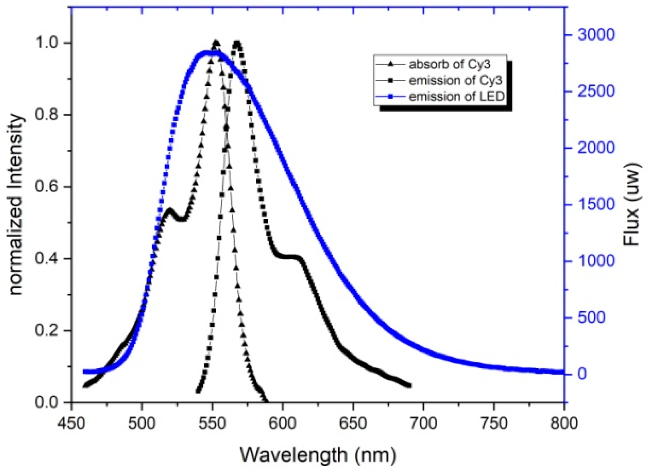
In the design setup, we use Cy3 fluorescence molecules as a reference material for fluorescence absorption. To achieve the largest light flux passing through the excitation filters of the microscope, the spectrum of the selected LED must fit the absorption spectrum of the Cy3 fluorescent molecules as closely as possible. A Lumileds LED (LXML-PX02-0000) made by Philips company was chosen to build up our light source system. The absorption and emission spectrum of the Cy3 fluorescent molecules and the spectrum of the selected LED are shown in Figure 1.
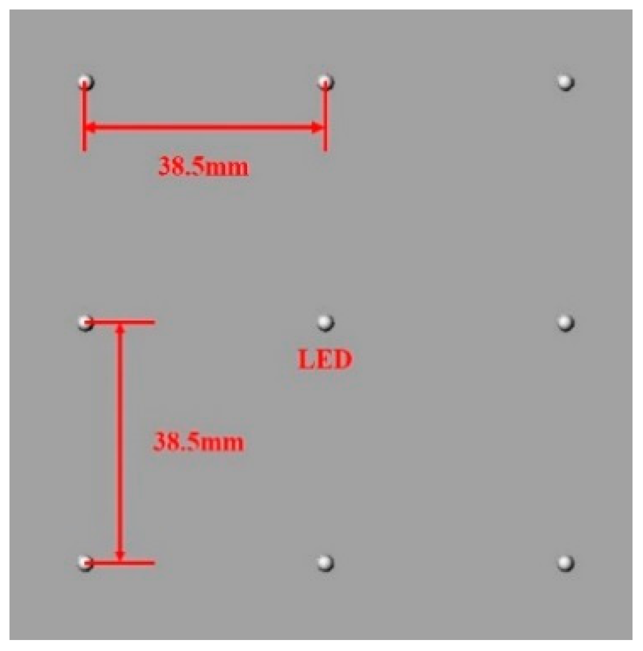
The luminous flux of the LED, which is measured by a 10-inch integrating sphere, is 143 lumens at 2.75 V (operating voltage) and 0.32 A (operating current). This luminous value will be used in the simulation to calculate the actual number of LEDs required. Based on the limitations of the fabrication and the measured luminous flux, we take 9 LEDs in a array to construct the lighting system. The distance between each LED in the array is 38.5 mm. The layout is shown in Figure 2.
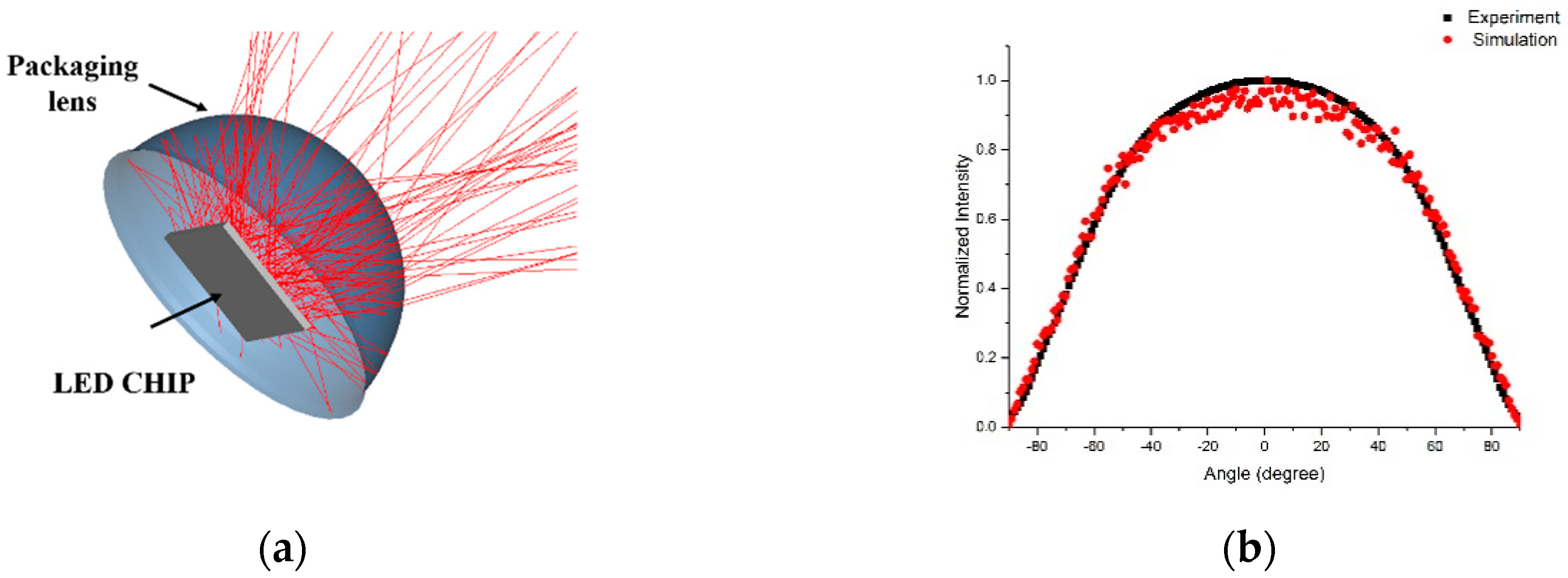
The Lumileds LED is a quasi-Lambertian LED. The emitting area of the LED is 1.06 mm × 1.06 mm, and the shape of the packaging lens is dome-like, with a radius of about 2.8 mm. Jacobson proposed a simple LED light source model construction in 2001 [43]. According to previous research by Sun [44,45,46,47], precision simulation results require constructing the structure of the LEDs to get the optical model of the single LED. The optical model of the LED is shown in Figure 3a. Further, the rays emitted from the LED are traced, and the corresponding normalized intensity distribution is calculated by the ASAP optical analysis software (Breault Research Organization, Inc. Tucson, AZ 85706 USA). The precision of the model is verified by comparing the LED intensity distribution from the experimental result with that from the simulation result.
The normalized intensity distribution comparison from the experimental result and that from the simulation result is shown in Figure 3b, in which the black and red dots respectively represent the experimental and simulation values. The accuracy of the optical model can also be verified by the normalized correlation coefficient (NCC) value that represents the similarity between the experimental result and the simulation result. It is obtained as follows,
where A(θn) and B(θn) are the experimental and simulation results, respectively, while and are the mean values. θn is the divergent angle of the LED. After calculation, the NCC value is 99.5%, which means that this optical model is accurate enough to be used in subsequent optical designs.
2.2. Optical Design of the CTLAS System
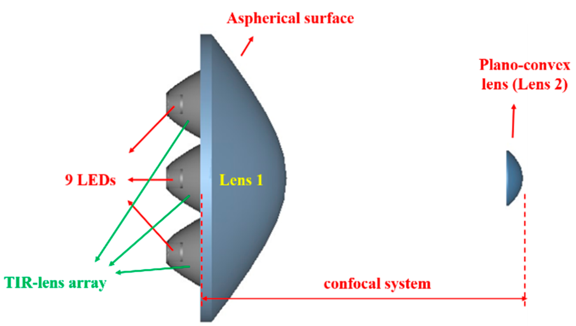
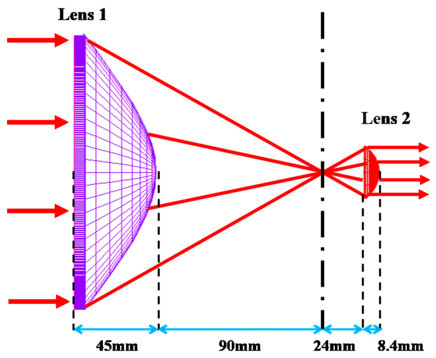
The light emitted from the quasi-Lambertian LEDs always diverges outward and requires convergence on the specimen to enhance the irradiation values. The CTLAS system we designed is composed of a TIR-lens array and a confocal system to efficiently collect the light energy of the LEDs array, as shown in Figure 4. In the CTLAS system, lens 1 is built up by attaching the TIR-lens array to the front lens of the confocal system as a one-piece lens. The left side of lens 1 is a TIR-lens array used to assemble the 9 LEDs.
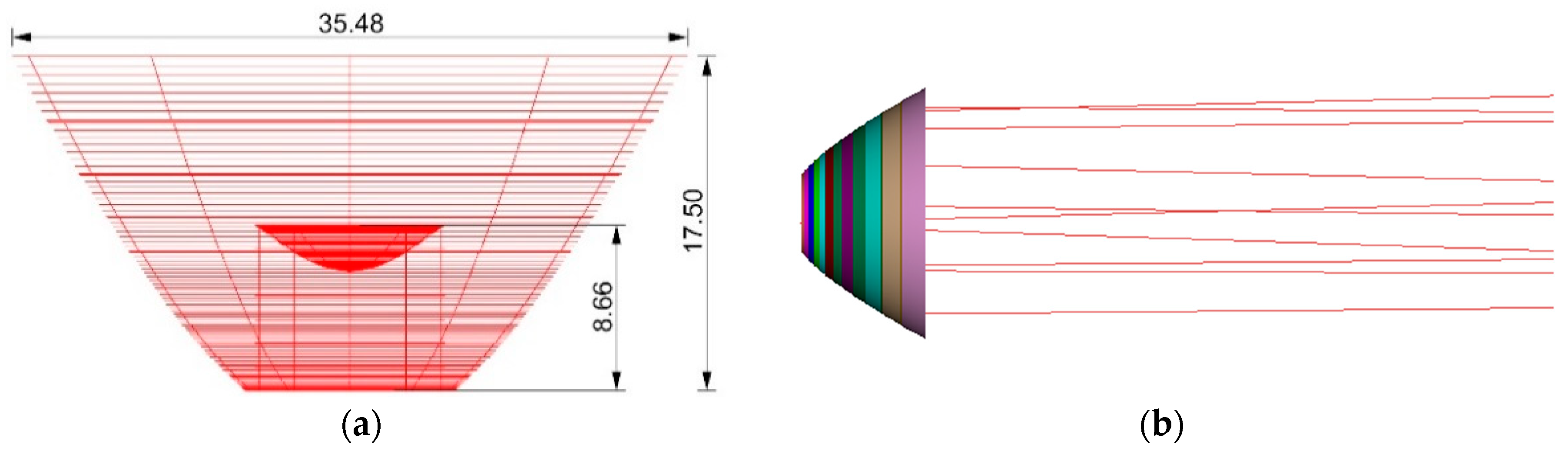
The TIR lens is designed to collimate the divergent light of a single LED with a total internal reflection effect, as shown in Figure 5a. The height and diameter of the designed TIR lens are, respectively, 17.5 mm and 35.5 mm, and the material is PMMA with a 1.49 refractive index.
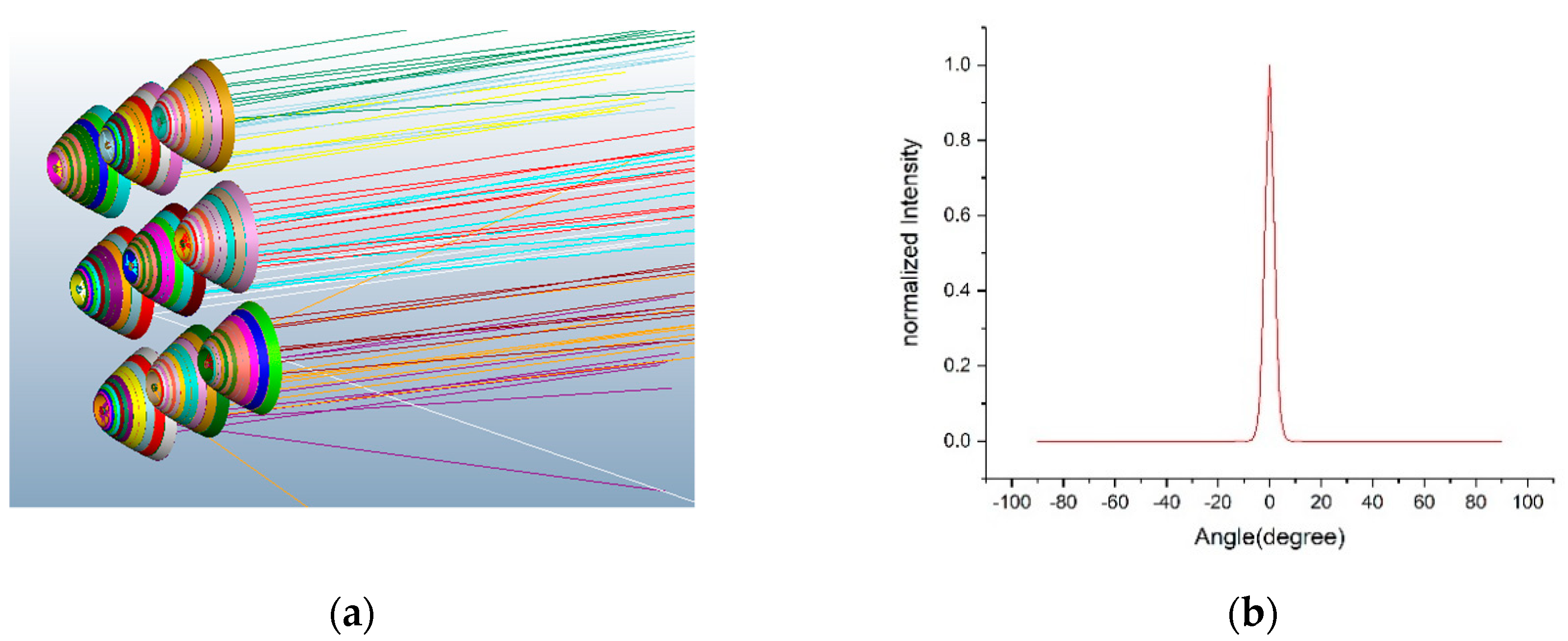
By ASAP, the ray tracing the result of the TIR lens is shown in Figure 5b. We can see that, after passing through the TIR lens, the divergent light is well collimated. In light of the testing performance, we further acquired the result that the TIR-lens array can collimate the divergent light from the 3 × 3 LED array and turn it into quasi-collimating light with a larger beam size, as shown in Figure 6a. The side length of the TIR-lens array is 106.5 mm, and the normalized intensity distribution of the TIR-lens array is shown in Figure 6b. According to the simulation results, the half-width-half-magnitude (HWHM) value of the normalized intensity distribution of the TIR-lens array is ±2.8°. The optical efficiency, defined as the ratio of the luminous flux of the TIR-lens array to the total luminous flux of the LED, is 91.7%.
In order to enhance the illuminance, the second surfaces of lens 1 and lens 2 form a confocal system. The quasi-collimating light of a larger beam size passing through the second surface of lens 1 is focused on its focal point, which is also the front focal point of lens 2. After that, the focal light will re-emerge from the focal point and form a small-size quasi-collimating light beam. As shown in Figure 7, lens 2 is a plano-convex lens.
The back surfaces of lenses 1 and 2 are both aspherical in order to eliminate the spherical aberration. Those surfaces are also calculated by the sag function [48] which can represent the shape of the aspherical surface and which is obtained by
where z(r), k, and A are the sag, conic constant, and the four-order aspherical coefficient of the aspherical surface, respectively. c is the curvature of the aspherical surface at its vertex, and r is the axial height on the aspherical surface. Thus, the second surfaces of lenses 1 and 2 are both designed and optimized by the Zemax software. The optimization values, c, k, and A, of the second surfaces of lenses 1 and 2 are shown in Table 1. In the confocal system, the distance between the second surface of lens 1 and the bottom plane of lens 2 is 114 mm; moreover, a mutual focal point is located 24 mm away from the bottom plane of lens 2. The diameters of lens 1 and lens 2 are 150 mm and 28 mm, respectively. The size of lens 2 is set to satisfy the size of the observation area on the specimen of the fluorescence microscope because the diameter of the observation area size must be 27 mm.
3. Results and Analyses
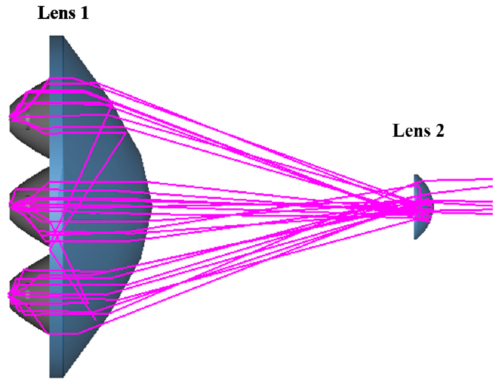
The ray tracing result of our designed CTLAS system by the ASAP software, shown in Figure 8.
The optical efficiency, defined as the ratio of the luminous flux of the LEDs and the output luminous flux emerging from lens 2, is obtained by
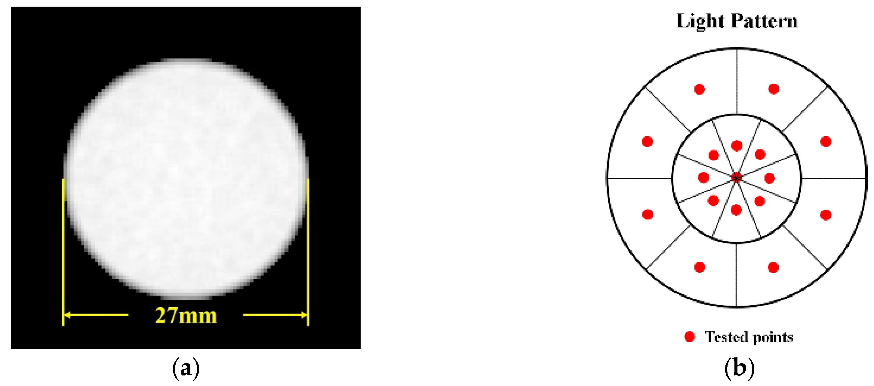
where FL and FO are, respectively, the luminous flux of the LEDs and the output luminous flux emerging from lens 2. In Figure 9a, the light pattern on the specimen is a 27 mm diameter circular area that is 550 mm away from the bottom of the LEDs. Figure 9b shows the uniformity of the light patterns calculated by the illuminance values of 17 tested points.
The red points show the testing positions. The uniformity of the light pattern is obtained by
where Eave and Emin are the average and the minimum irradiation values of the light pattern on the specimen. After the calculation, the optical efficiency of this system is 72.7%. The uniformity of the light pattern is 1.14, and the central irradiation value of the light pattern is 62,950 lux. The result surpassed the requirement of the illumination value of our initial setting.
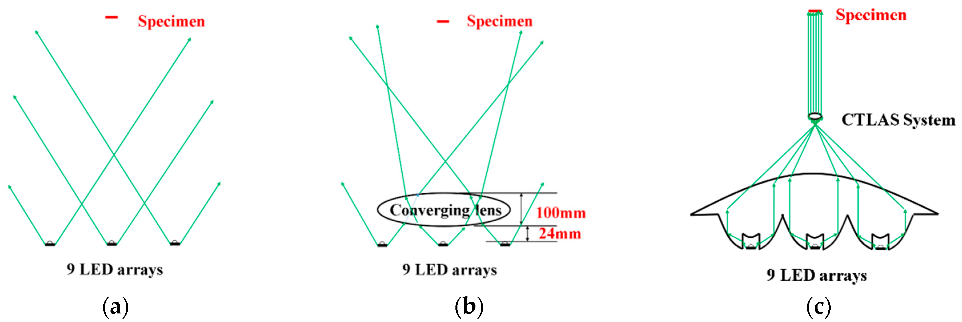
In a commercial fluorescence microscope system, most LED light sources are just used to illuminate the specimen without any additional components to collect light. Some LED light sources are attached with a converging lens to enhance the illuminance. Therefore, we take three examples, a nine-LED array, a nine-LED array with a converging lens, and the CTLAS system, to compare the illuminance, as shown in Figure 10.
In Figure 10b, a 150 mm diameter and 0.7 NA value converging lens are assembled at the center of the nine-LED array; the distance between the two is the focal length of the converging lens. The corresponding central illuminance and the uniformity of these three examples are shown in Table 2. The result shows that the CTLAS system obviously has the best uniformity and the greatest center illumination value, which is 46 times brighter than the nine-LED array and 40 times brighter than the nine-LED array with the converging lens.
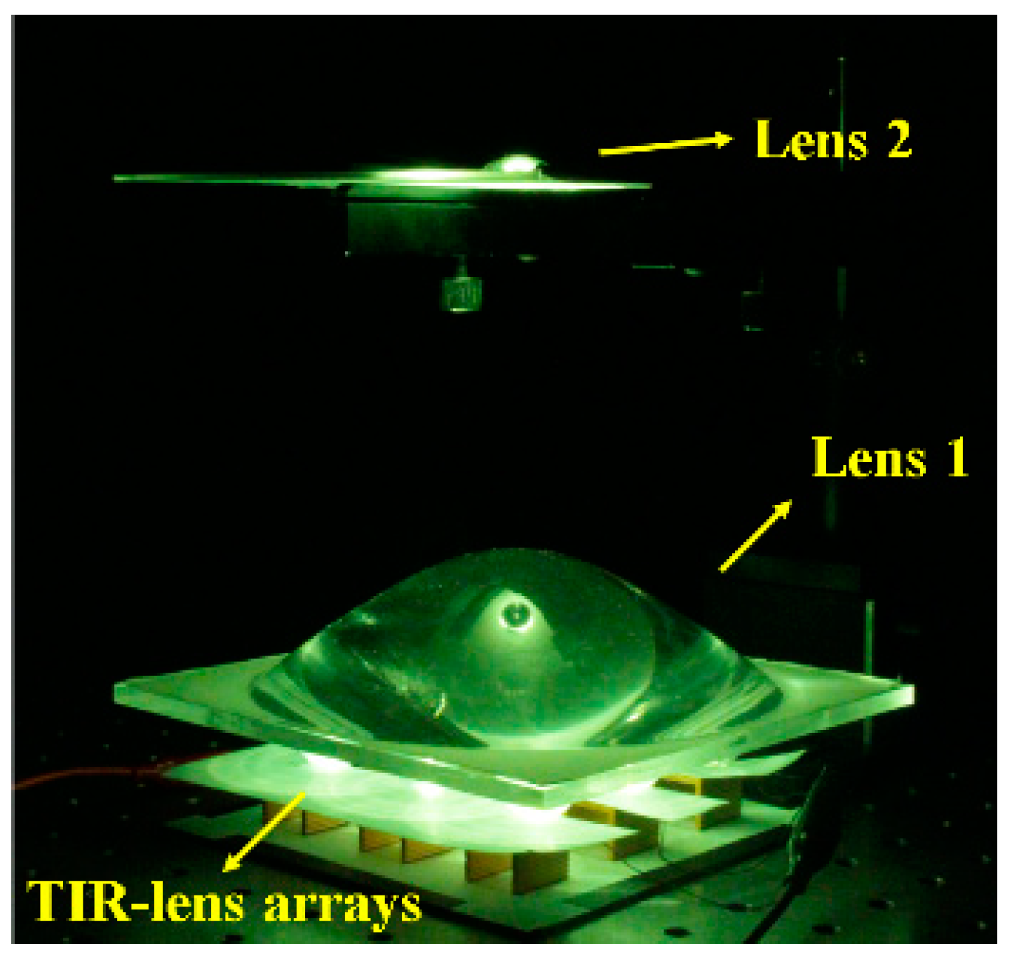
We successfully assembled the LED array and the CTLAS system. The system picture is shown in Figure 11.
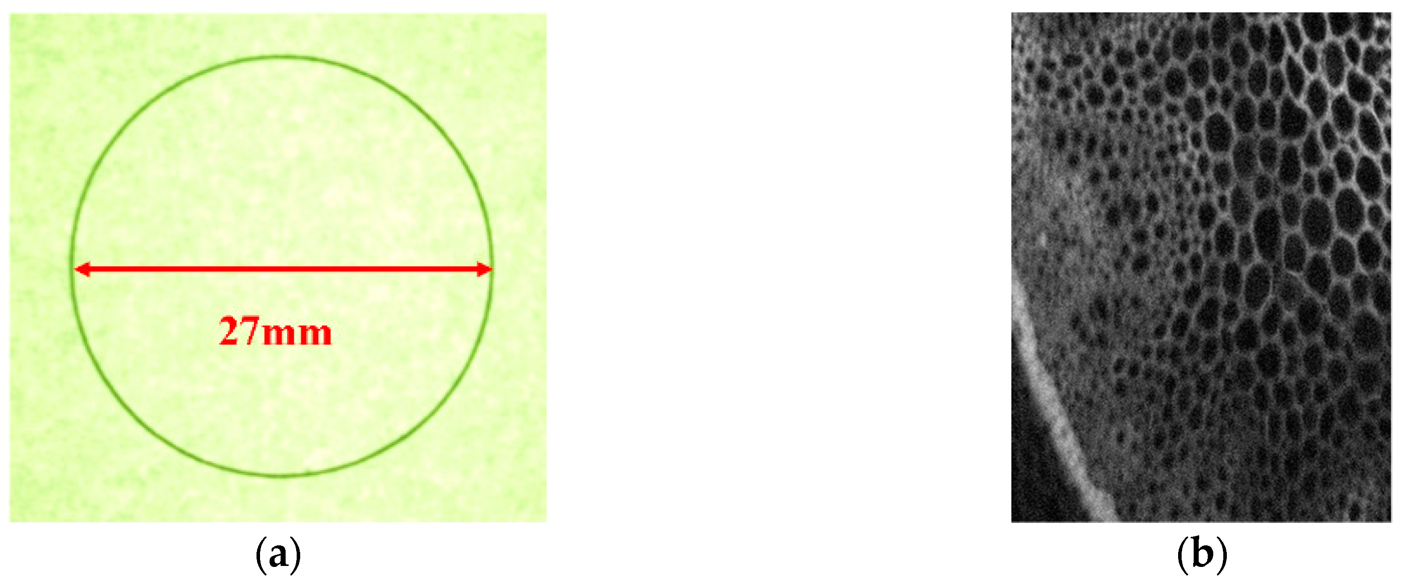
All the lenses in this system are made by mold injection. We used the CTLAS system to observe the fluorescent images of the vascular bundle organization modified with the Cy3 fluorescence molecules. The light pattern and fluorescent images of the vascular bundle organization modified with the Cy3 fluorescent molecules are shown in Figure 12. As shown, this CTLAS light source system can provide sufficient light for fluorescence microscopes.
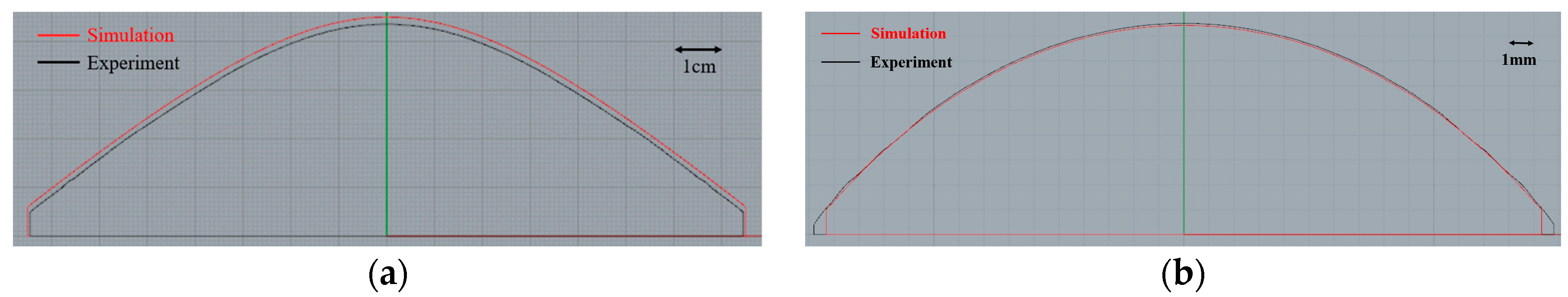
In the illumination test of the CTLAS light source system, the measurement data are lower than those of the simulation. Therefore, we checked the lens used in the system and found that there were minor deformations and errors in the two lenses. These deformations and errors come from the mold injection fabrication process. The shape errors of the second surfaces of lenses 1 and 2 are shown in Figure 13. The black and red lines in Figure 13 represent the measured and simulated lens shapes, respectively.
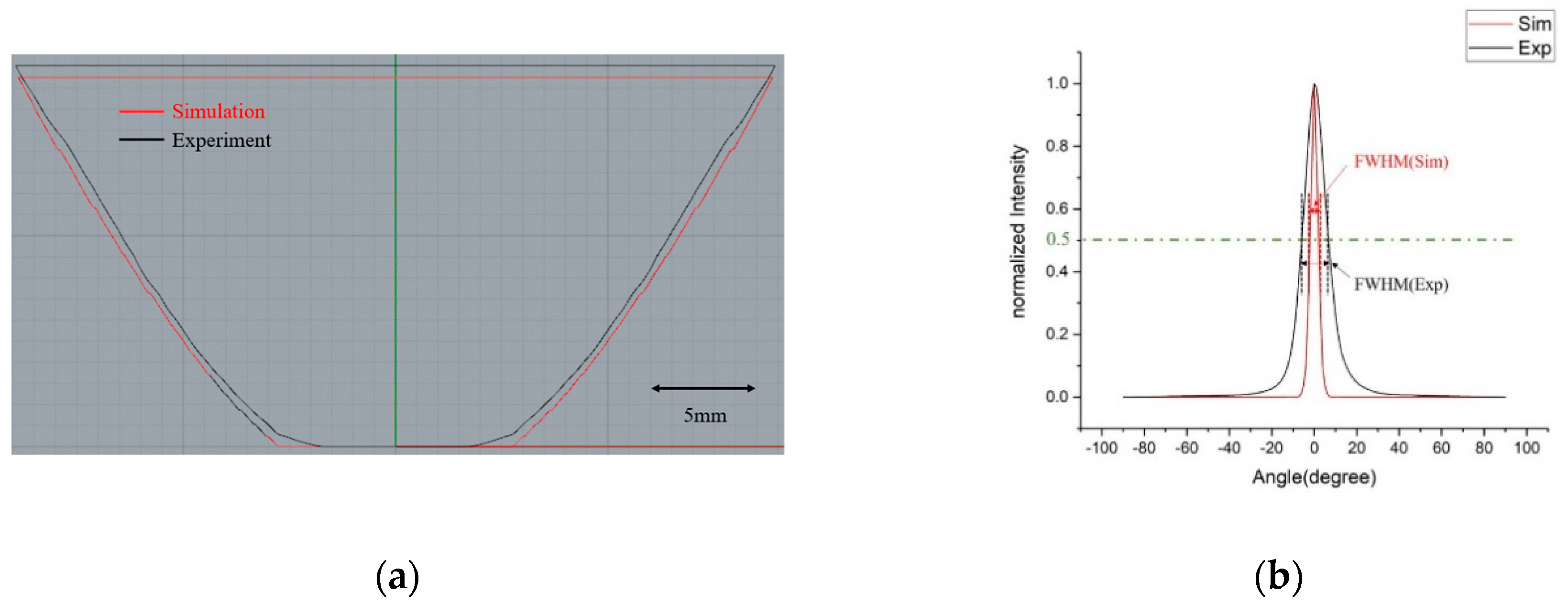
Figure 14 shows the shape error of the first surface of lens 1, which is composed of TIR-lens arrays and the normalized light intensity distributions from the simulation and the experimental results. The measured light intensity in Figure 14b shows that the full width at half maximum (FWHM) of the assembled CTLAS light source system is wider than that of the simulation, which indicates that the energy of the projecting light beam from the system is not sufficiently concentrated.
The errors of the finished TIR-lens array cause the divergence of the light beam; moreover, the energy of the light pattern is not sufficiently dense, due to the larger divergent angle. Hence, the measured illumination at the center of the light beam dropped to 980 lux. Taking the wrong parameters in the simulation, we acquired the central illumination of the light pattern of 1307 lux. The measured and simulated values are approximately in the same order of magnitude. This result demonstrates that the design method of the CTLAS system is feasible in the applications of LEDs applied in fluorescence microscopes.
4. Tolerance Analyses of the Light Source Assembly
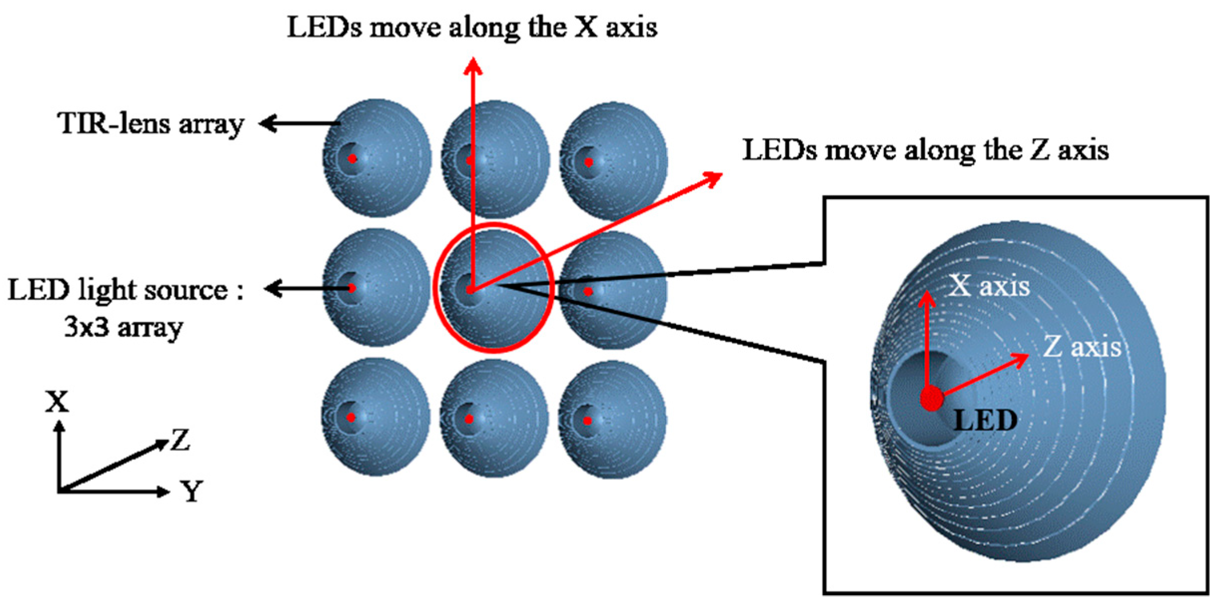
In order to achieve the highest yield rate of the production in the future, the alignment precision of the LEDs and TIR lens array is also a key point of the central illumination values. In the system assembly processes, owing to the symmetric rotational shape of the TIR lens, the effects of LEDs moving along the x-axis and y-axis are the same. Hence, LEDs can move in two directions, along the x-axis and the z-axis, as shown in Figure 15. We evaluated and analyzed the impact on precision affected by the misalignment.
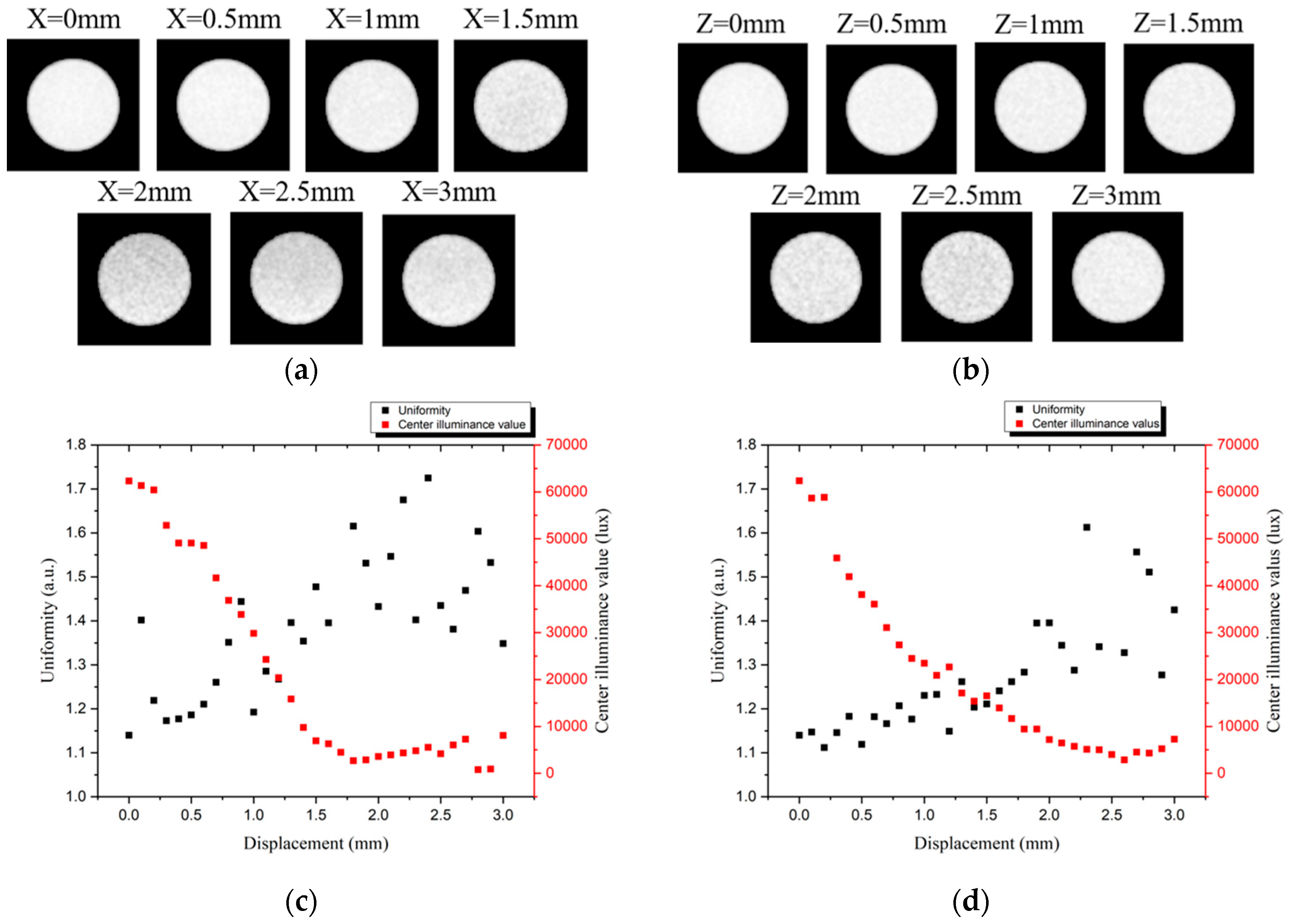
The corresponding uniformity and the central illumination values of the light pattern will change along with the increasing or decreasing distance between the LEDs and the TIR-lens array. In the example of 9 LEDs moving along the x-direction, Figure 16a,c show the simulation results of the light patterns and the central illuminance values, respectively, and Figure 16b,d show the simulation results for moving along the z-direction. In both of these examples, although moving in different directions, their central illumination values gradually reduced with increasing displacement from 0 mm to approximately 2 mm. After 2 mm of displacement, the values tend to be stable.
The uniformity of the light patterns shows some oscillations with increasing displacement, and the uniformity still exhibits a gradually rising trend. This means that the LED misalignment will cause light patterns to be darker and non-uniform. Moreover, regarding both uniformity and the center illuminance, the increasing displacement of the x-axis causes bigger values to change compared with the situation of the z-axis. On the one hand, in the x-axis, the non-uniformity and the reduced brightness come from both the skewness of the projecting light and the hot spot laterally leaving the central point. On the other hand, these variations are affected by the defocusing effect of the LED array in the z-axis. The defocused light from the adjacent TIR lenses is diffused, and there is interference between light from different lenses, which reduces the uniformity.
To meet the initial specifications that the center illuminance of a fluorescence microscope is 10,578 lux, the tolerances of the LED displacement along the x-axis and along the z-axis must be controlled within 1.3 mm and 1.7 mm, respectively, and the corresponding uniformity is 1.39 and 1.26.
5. Conclusions
Research on the light sources of commercial microscopes or for other specific purposes plays a significant role in biomedical scientists’ study. In this paper, we reveal a design method for LED light sources applied in fluorescence microscopes. In our case, the target fluorescent molecules are Cy3; however, this design method is not limited to Cy3 molecules. In light of the design concept, all of the commercial fluorescent molecules can be applied. We have demonstrated and assembled the CTLAS light source system successfully. Our CTLAS light source system is composed of a nine-LED array, the corresponding TIR lens array and the confocal system that can collimate divergent light emitted from the LED array and reduce the beam size to provide a circular light pattern on the specimen with higher illuminance.
All recipes and optical component models are simulated in ASAP optical software. We have taken both common cases, a nine-LED array only and a nine-LED array with a converging lens with our designed CTLAS light source system to compare the illuminance. The simulation result shows that this CTLAS system has the best uniformity and the greatest center illumination which is 46 times brighter than only using the nine-LED array mode and 40 times brighter than using the nine-LED array with a converging lens. In the evaluation of the misalignment for the CTLAS system assembly, the skewness of the projecting light and the hot spot laterally leaving the central point on the x-axis have a greater impact on the uniformity and illuminance than the defocusing effect on the z-axis. The tolerances of the LED displacement on the x-axis and z-axis must be controlled within 1.3 mm and 1.7 mm, respectively, so that the illuminance can reach the initial settings; the corresponding uniformity is 1.39 and 1.26. In consideration of energy saving, the total electric power of the LED array is 7.9 watts, which is approximately 6.6% of the original white halogen lamp used in an Axio Imager 2 fluorescence microscope. Moreover, according to the simulation results, the central illuminance value of the light pattern projected by the microscope that we designed is 62,950 lux, which is about 5.95 times that of a microscope with the original white halogen lamp (10,578 lux). The results of our study provide an optical design that demonstrates the use of LEDs to replace the traditional energy-consuming light source.
Author Contributions
T.-C.K. provided the research resources, the fluorescence microscopy and the Cy3 test sample. T.-J.D. was responsible for the completion of the experimental and simulation work. J.-H.L. assisted in the writing of this article. S.-H.M. proposed the whole ideas and controlled the progress of this research.
Funding
This research is funded by the Ministry of Science and Technology of the Republic of China.
Acknowledgments
This work was supported by the Ministry of Science and Technology of the Republic of China, project MOST 107-2221-E-035-056.
Conflicts of Interest
The authors declare no conflict of interest.
References
- Alfano, R.; Alimova, A.; Vidyasagar, S.; Katz, A. Phosphorescence And Fluorescence Measurements of Human Tissues Using UV LED Excitation. In Proceedings of the Biomedical Optics, Fort Lauderdale, FL, USA, 19–22 March 2006; p. TuD7. [Google Scholar]
- Egorova, O.; Egorov, M. Development Trends in Light Microscopy. J. Opt. Technol. 2011, 78, 7–18. [Google Scholar] [CrossRef]
- Park, Y.; Popescu, G.; Badizadegan, K.; Dasari, R.; Feld, M. Diffraction Phase and Fluorescence Microscopy. Opt. Express 2006, 14, 8263–8268. [Google Scholar] [CrossRef]
- Steigerwald, D.; Bhat, J.; Collins, D.; Fletcher, R.; Holcomb, M.; Ludowise, M.; Martin, P.; Rudaz, S. Illumination with Solid State Lighting Technology. IEEE Photonics Soc. 2002, 8, 310–320. [Google Scholar] [CrossRef]
- Narukawa, Y. White-Light LEDs. Opt. Photonics News 2004, 15, 24–29. [Google Scholar] [CrossRef]
- Žukauskas, A.; Shur, M.; Gaska, R. Introduction to Solid-State Lighting; JohnWiley & Sons Pte Ltd.: New York, NY, USA, 2002. [Google Scholar]
- Schubert, E. Light-Emitting Diodes, 2nd ed.; Cambridge University Press: Cambridge, UK, 2006. [Google Scholar]
- Shieh, J.; Wang, L.; Chiu, M. A High Color Rendering Index on Multichip LED Light Source. Circuits Syst. 2012, 3, 107–110. [Google Scholar] [CrossRef] [Green Version]
- Schubert, E. Solid-State Light Sources Getting Smart. Science 2005, 308, 1274–1278. [Google Scholar] [CrossRef]
- Liu, S.; Luo, X.B. LED Packaging for Lighting Applications; JohnWiley & Sons Pte Ltd.: New York, NY, USA, 2011. [Google Scholar]
- MacIsaac, D.; Kanner, G.; Anderson, G. Basic Physics of the Incandescent Lamp (Lightbulb). Phys. Teach. 1999, 37, 520–525. [Google Scholar] [CrossRef]
- Herman, P.; Maliwal, B.; Lin, H.; Lakowicz, J. Frequency-Domain Fluorescence Microscopy with the LED as a Light Source. J. Microsc. 2001, 203, 176–181. [Google Scholar] [CrossRef]
- Hohman, B. LED Light Source: Major Advance in Fluorescence Microscopy. Microsc. Today 2008, 16, 28–29. [Google Scholar] [CrossRef] [Green Version]
- Bormuth, V.; Howard, J.; Schäffer, E. LED Illumination For Video-Enhanced DIC Imaging of Single Microtubules. J. Microsc. 2007, 226, 1–5. [Google Scholar] [CrossRef]
- Hänscheid, T. The Future Looks Bright: Low-Cost Fluorescent Microscopes for Detection of Mycobacterium Tuberculosis and Coccidiae. Trans. R. Soc. Trop. Med. Hyg. 2008, 102, 520–521. [Google Scholar] [CrossRef]
- Albeanu, D.; Soucy, E.; Sato, T.; Meister, M.; Murthy, V. LED arrays as cost effective and efficient light sources for widefield microscopy. PLoS ONE 2008, 3, e2146. [Google Scholar] [CrossRef]
- Akifumi, H.; Satoshi, H.; Martin, V. Single-Molecule imaging with an inexpensive UV-LED light source. Chem. Lett. 2009, 38, 234–235. [Google Scholar]
- Gerhardt, I.; Mai, L.; Lamas-Linares, A.; Kurtsiefer, C. Detection of Single Molecules Illuminated by a Light-Emitting Diode. Sensors 2011, 11, 905–916. [Google Scholar] [CrossRef] [Green Version]
- Breslauer, D.; Maamari, R.; Switz, N.; Lam, W.; Fletcher, D. Mobile Phone Based Clinical Microscopy for Global Health Applications. PLoS ONE 2009, 4, e6320. [Google Scholar] [CrossRef]
- Miller, A.; Davis, G.; Oden, Z.; Razavi, M.; Fateh, A.; Ghazanfari, M.; Abdolrahimi, F.; Poorazar, S.; Sakhaie, F.; Olsen, R.; et al. Portable, Battery-Operated, Low-Cost, Bright Field and Fluorescence Microscope. PLoS ONE 2010, 5, e11890. [Google Scholar] [CrossRef]
- Schaefer, S.; Boehm, S.; Chau, K. Automated, Portable, Low-Cost Bright-Field and Fluorescence Microscope with Autofocus and Autoscanning Capabilities. Appl. Opt. 2012, 51, 2581–2588. [Google Scholar] [CrossRef]
- Brydegaard, M.; Merdasa, A.; Jayaweera, H.; Ålebring, J.; Svanberg, S. Versatile Multispectral Microscope Based on Light Emitting Diodes. Rev. Sci. Instrum. 2011, 82, 123106. [Google Scholar] [CrossRef]
- Shin, D.; Pierce, M.; Gillenwater, A.; Williams, M.; Richards-Kortum, R. A Fiber-Optic Fluorescence Microscope Using a Consumer-Grade Digital Camera For in Vivo Cellular Imaging. PLoS ONE 2010, 5, e11218. [Google Scholar] [CrossRef]
- Cybulski, J.; Clements, J.; Prakash, M. Foldscope: Origami-Based Paper Microscope. PLoS ONE 2014, 9, e98781. [Google Scholar] [CrossRef]
- Heng, J.; Qian, K. Designing Single LED Illumination Distribution for Direct-Type Backlight. Appl. Opt. 2013, 52, 7022–7027. [Google Scholar]
- Feng, Q.; Li, Y.; Li, Q.; Lv, G. Secondary Optical Design for LED Backlight Luminance Improvement of Helmet-Mounted Display. J. Disp. Technol. 2016, 12, 577–582. [Google Scholar] [CrossRef]
- Wu, F.; Li, S.; Zhang, X.; Ye, W. A Design Method for LEDs Arrays Structure Illumination. J. Disp. Technol. 2016, 12, 1177–1184. [Google Scholar] [CrossRef]
- Pal, S. Optimization of LED Array For Uniform Illumination Over A Target Plane By Evolutionary Programming. Appl. Opt. 2015, 54, 8221–8227. [Google Scholar] [CrossRef]
- Moreno, I. Image-Like Illumination with LED Arrays: Design. Opt. Lett. 2012, 37, 839–841. [Google Scholar] [CrossRef]
- Shen, S.; Huang, H. Design of LED Fish Lighting Attractors Using Horizontal/Vertical LIDC Mapping Method. Opt. Express 2012, 20, 26135–26146. [Google Scholar] [CrossRef]
- Zhu, Z.; Qu, X.; Jia, G.; Ouyang, J. Uniform Illumination Design by Configuration of LED Array and Diffuse Reflection Surface for Color Vision Application. J. Disp. Technol. 2011, 7, 84–89. [Google Scholar] [CrossRef]
- Kari, T.; Gadegaard, J.; Jørgensen, D.; Søndergaard, T.; Pedersen, T.; Pedersen, K. Compact Lens with Circular Spot Profile for Square Die LEDs in Multi-LED Projectors. Appl. Opt. 2011, 50, 4860–4867. [Google Scholar] [CrossRef]
- Wu, R.; Liu, P.; Zhang, Y.; Zheng, Z.; Li, H.; Liu, X. A Mathematical Model of the Single Freeform Surface Design for Collimated Beam Shaping. Opt. Express 2013, 21, 20974–20989. [Google Scholar] [CrossRef]
- Li, S.; Chen, F.; Wang, K.; Zhao, S.; Zhao, Z.; Liu, S. Design of a Compact Modified Total Internal Reflection Lens for High Angular Color Uniformity. Appl. Opt. 2012, 51, 8557–8562. [Google Scholar] [CrossRef]
- Jafrancesco, D.; Mercatelli, L.; Sansoni, P.; Fontani, D.; Sani, E.; Coraggia, S.; Meucci, M.; Francini, F. Optical Design of a Light-Emitting Diode Lamp for a Maritime Lighthouse. Appl. Opt. 2015, 54, 3252–3262. [Google Scholar] [CrossRef]
- Wang, G.; Wang, L.; Li, F.; Zhang, G. Collimating Lens for Light-Emitting-Diode Light Source Based on Non-Imaging Optics. Appl. Opt. 2012, 51, 1654–1659. [Google Scholar] [CrossRef]
- Chen, C.; Zhang, X. Design of Optical System for Collimating the Light of an LED Uniformly. J. Opt. Soc. Am. A 2014, 31, 1118–1125. [Google Scholar] [CrossRef]
- Chen, J.; Huang, Z.; Liu, T.; Tsai, M.; Huang, K. Freeform Lens Design for Light-Emitting Diode Uniform Illumination by Using a Method of Source–Target Luminous Intensity Mapping. Appl. Opt. 2015, 54, E146–E152. [Google Scholar] [CrossRef]
- Chen, R. Investigation of a Slope-Point-Based Method for the Design of Aspheric Surfaces in a Catadioptric Collimating Optical System for a Light-Emitting Diode Source. Appl. Opt. 2014, 53, H129–H139. [Google Scholar] [CrossRef]
- Amos, W.; White, J.; Fordham, M. Use of Confocal Imaging in the Study of Biological Structures. Appl. Opt. 1987, 26, 3239–3243. [Google Scholar] [CrossRef]
- Sung, K.; Richards-Kortum, R.; Follen, M.; Malpica, A.; Liang, C.; Descour, M. Fiber Optic Confocal Reflectance Microscopy: A New Real-Time Technique To View Nuclear Morphology in Cervical Squamous Epithelium In Vivo. Opt. Express 2003, 11, 3171–3181. [Google Scholar] [CrossRef]
- Dobson, S.; Sun, P.; Fainman, Y. Diffractive Lenses for Chromatic Confocal Imaging. Appl. Opt. 1997, 36, 4744–4748. [Google Scholar] [CrossRef]
- Jacobson, B.; Gengelbach, R. Lens for Uniform LED Illumination: An Example of Automated Optimization Using Monte Carlo Ray-Tracing of an LED Source. In Nonimaging Optics: Maximum Efficiency Light Transfer VI; SPIE: Bellingham, WA, USA, 2001. [Google Scholar]
- Sun, C.; Lee, T.; Ma, S.; Lee, Y.; Huang, S. Precise optical modeling for LED lighting verified by cross correlation in the midfield region. Opt. Lett. 2006, 31, 2193–2195. [Google Scholar] [CrossRef]
- Chien, W.; Sun, C.; Moreno, I. Precise Optical Model of Multi-Chip White LEDs. Opt. Express 2007, 15, 7572–7577. [Google Scholar] [CrossRef]
- Sun, C.; Chen, C.; He, H.; Chen, C.; Chien, W.; Lee, T.; Yang, T. Precise optical modeling for silicate-based white LEDs. Opt. Express 2008, 16, 20060–20066. [Google Scholar] [CrossRef] [PubMed]
- Sun, C.; Chang, Y.; Wang, Y.; Chen, C.; Lo, Y.; Cheng, H. Precise Spatial-Color Optical Modeling in Phosphor-Converted White LEDs. J. Disp. Technol. 2015, 11, 261–265. [Google Scholar] [CrossRef]
- Mahajan, V. Fundamentals of Geometrical Optics, 1st ed.; SPIE—The International Society for Optical Engineering: Bellingham, WA, USA, 2014. [Google Scholar]
Figure 1.
The absorption and emission spectrum of Cy3 fluorescent molecules, and the emission spectrum of the selected LED.
Figure 1.
The absorption and emission spectrum of Cy3 fluorescent molecules, and the emission spectrum of the selected LED.

Figure 2.
The layout of the 3 × 3 LEDs array.

Figure 3.
(a) The optical model of the LED, (b) the normalized intensity distribution comparison of the experimental result and the simulation result.
Figure 3.
(a) The optical model of the LED, (b) the normalized intensity distribution comparison of the experimental result and the simulation result.

Figure 4.
Optical setup of the confocal total internal reflection lens array system (CTLAS) system.

Figure 5.
(a) The structure of the designed total internal reflection (TIR) lens (the values are in mm), (b) the ray tracing the result of the TIR lens.
Figure 5.
(a) The structure of the designed total internal reflection (TIR) lens (the values are in mm), (b) the ray tracing the result of the TIR lens.

Figure 6.
The designed 3 × 3 TIR-lens array, (a) the ray tracing simulation result, (b) the corresponding normalized intensity distribution.
Figure 6.
The designed 3 × 3 TIR-lens array, (a) the ray tracing simulation result, (b) the corresponding normalized intensity distribution.

Figure 7.
The setup of the CTLAS system. It is composed of a two-lens confocal system.

Figure 8.
The ray tracing result of the CTLAS system.

Figure 9.
(a) The circular light pattern on the specimen, (b) the uniformity of the light pattern calculated by the illuminance values of the 17 tested red points.
Figure 9.
(a) The circular light pattern on the specimen, (b) the uniformity of the light pattern calculated by the illuminance values of the 17 tested red points.

Figure 10.
The three types of LED light sources, (a) the nine-LED array only, (b) the nine-LED array with the converging lens, and (c) the nine-LED array with the CTLAS system.
Figure 10.
The three types of LED light sources, (a) the nine-LED array only, (b) the nine-LED array with the converging lens, and (c) the nine-LED array with the CTLAS system.

Figure 11.
The assembled CTLAS system.

Figure 12.
(a) The light pattern of the CTLAS system, (b) fluorescent images of the vascular bundle organization modified with the Cy3 fluorescent molecules.
Figure 12.
(a) The light pattern of the CTLAS system, (b) fluorescent images of the vascular bundle organization modified with the Cy3 fluorescent molecules.

Figure 13.
The shape errors between finished lens and simulation, (a) lens 1, (b) lens 2.

Figure 14.
The comparison results of (a) the shapes of the experimental and the simulation TIR lenses, (b) the corresponding normalized light intensity distributions.
Figure 14.
The comparison results of (a) the shapes of the experimental and the simulation TIR lenses, (b) the corresponding normalized light intensity distributions.

Figure 15.
The movements of the 9-LED array along the x-axis and the z-axis.

Figure 16.
The light patterns of the 9-LED array move along (a) the x-axis, and (b) the z-axis. The central illumination values and uniformity of different displacements along (c) the x-axis, and (d) the z-axis.
Figure 16.
The light patterns of the 9-LED array move along (a) the x-axis, and (b) the z-axis. The central illumination values and uniformity of different displacements along (c) the x-axis, and (d) the z-axis.


Table 1.
The c, k, and A values of the 2nd surfaces of lens 1 and lens 2.
| c | k | A | |
|---|---|---|---|
| Lens1 | −46.65 | −2.3 | 0 |
| Lens2 | −15.3 | −0.654 | −3.928 × 10⁻⁶ |
Table 2.
The simulation results of the central illuminance values and the uniformity of the nine-LED array, the nine-LED array with the converging lens and the CTLAS system.
Table 2.
The simulation results of the central illuminance values and the uniformity of the nine-LED array, the nine-LED array with the converging lens and the CTLAS system.
| 9-LED Array | 9-LED Array with Converging Lens | 9-LED Array with the CTLAS System | |
|---|---|---|---|
| Central illuminance value (Lux) | 1377 | 1590 | 62,950 |
| Uniformity | 2 | 1.81 | 1.14 |
© 2019 by the authors. Licensee MDPI, Basel, Switzerland. This article is an open access article distributed under the terms and conditions of the Creative Commons Attribution (CC BY) license (http://creativecommons.org/licenses/by/4.0/).
Share and Cite
MDPI and ACS Style
Kuo, T.-C.; Ding, T.-J.; Lin, J.-H.; Ma, S.-H. Optical Design of an LED Lighting Source for Fluorescence Microscopes. Appl. Sci. 2019, 9, 4574. https://0-doi-org.brum.beds.ac.uk/10.3390/app9214574
AMA Style
Kuo T-C, Ding T-J, Lin J-H, Ma S-H. Optical Design of an LED Lighting Source for Fluorescence Microscopes. Applied Sciences. 2019; 9(21):4574. https://0-doi-org.brum.beds.ac.uk/10.3390/app9214574
Chicago/Turabian StyleKuo, Tai-Chih, Ting-Jou Ding, Jui-Hui Lin, and Shih-Hsin Ma. 2019. "Optical Design of an LED Lighting Source for Fluorescence Microscopes" Applied Sciences 9, no. 21: 4574. https://0-doi-org.brum.beds.ac.uk/10.3390/app9214574
Note that from the first issue of 2016, this journal uses article numbers instead of page numbers. See further details here.