1. Introduction
Since Davydov et al. discovered the narrow band gap phenomenon of InN (
Eg~0.7 eV), InN has attracted a wide range of research interest [
1]. In addition, we expect InN to have the highest electron mobility among III-nitrides (approximately 4400 cm
2/V∙S). These characteristics will enable InN to be considered a highly potential application material in many optoelectronic fields, such as high-speed electronic devices (HEMT), optoelectronic detectors, and photovoltaic and light-emitting devices [
2,
3,
4,
5]. However, due to a large number of external defects such as dislocation, defects, and so on, practical InN-based devices are still not achievable [
6,
7]. In addition, the Fermi energy level pinning above the conduction band is accompanied by a donor-like surface state, resulting in an ultrahigh density of the surface electron accumulation layer.
Most InN samples reported recently are
n-type degenerate semiconductors, with an electron concentration of approximately 1 × 10
18 cm
−3 or higher. Much research has been dedicated to understanding the fundamental properties of InN, especially its photoluminescence (PL) properties [
8,
9,
10,
11]. The optical properties of semiconductors are very sensitive to the increase in carrier concentration and are reflected in the blueshift of peak energy and the expansion of the peak width. Many research teams have recently discussed the origin of the high emission peaks above the theoretical bandgap (~0.65 eV) in degenerate InN samples [
11,
12]. This high-energy peak has been ascribed to Mahan excitons and inspected by PL spectra and reflectivity measurement [
12].
As III-V nitrides lack native substrates for these materials, there is a very large dislocation density in the film. As a result, the crystalline quality of these materials is reduced, which leads to a reduction in practical performance. As with other III-V nitrides, bulk InN also lacks a native substrate. Fortunately, the nanometer-scale quasi-one-dimensional (quasi-1D) structure has become a subject of intense research interest due to the low structural defect density [
13,
14]. This nanostructure shows promising potential for the realization of both fundamental physical research and the improvement of electronic, optoelectronic, and chemical/biological sensing properties with nanodevices. The morphology of quasi-1D InN, including nanorods, nanowires, nanotips, nanotubes and nanobelts, has been reported [
15,
16,
17]. The intrinsic characteristic of electron accumulation at the InN surface has been considered for developing high-sensitivity vapor/liquid detection devices [
18,
19]. Several growth techniques have been used for the fabrication of InN nanostructures, with vapor-liquid-solid (VLS) catalytic growth from the bottom up being the most used method [
20,
21,
22]. There is also the option of utilizing a catalyst for growth, but this requires a material that is liquefied and inert below the growth temperature.
Instead of a catalyst-assisted process, this study demonstrates a self-catalysis mechanism for the growth of InN nanorods by controlling the temperature through metal-organic molecular-beam epitaxy (MOMBE). The optical properties and carrier dynamics of InN samples, including film-type, nanorod-type, and mixed-type, were studied at different carrier concentrations (higher than 1 × 1018 cm−3) using PL, time-resolved photoluminescence (TRPL), and Raman spectra. High-energy transitions appeared above the bandgap value of 0.7 eV, which was classified to the presence of Mahan excitons. We adopt the TRPL technique to further confirm the evidence of the presence of Mahan excitons, in which the spectra revealed a strong localization phenomenon near the Mahan excitons’ energy.
2. Results and Discussions
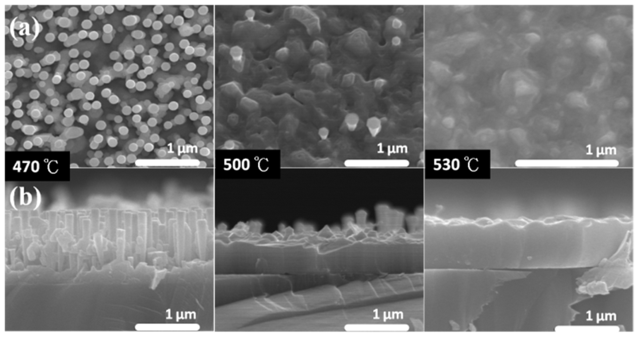
Figure 1 shows the top-view and cross-sectional SEM images of InN materials grown at various temperatures, and the structure of InN transitioned from 1D nanorods to 2D thin films with increasing growth temperature. The length and diameter of the nanorods were determined to be approximately 1.05 μm and 160 nm, respectively. As the growth temperature increased, the surface became rougher with the coexistence of both nanorods and a film structure. The initial thickness of the film was approximately 580 nm, but this increased to a maximum of 880 nm at the highest growth temperature.
Table 1 lists detailed structural information of the InN samples.
As can be seen from our experimental results, the two-dimensional InN layer tends to form at higher growth temperatures, while 1D nanorods form at lower growth temperatures. In addition, the presence of metal droplets was not observed at the end of the 1D nanorod structure, which may elucidate the nanorods’ growth through the self-catalytic process. In our experiment, the growth rate increased with the III/V flow ratio, which implies that the growth was in the N-rich regime, which is consistent with that reported by Yoshizawa et al. [
23]. According to earlier literature, the growth conditions of the N-rich regime can inhibit the formation of indium droplets; if no indium droplets appear, we may hypothesize that InN nanorods were grown through a no-catalytic-growth mechanism. Although no metal particles were observed at the top, we could not completely rule out the possibility of a VLS-like or self-catalyzed mechanism, as In atoms could desorb at high temperatures [
24,
25,
26,
27]. The pronounced 2D growth mode is related to the breakdown of anisotropic-directed growth at higher growth temperatures, and increased surface atomic mobility may cause more indium atoms to spread to the (0001) surface, providing more stable binding sites. At the lower temperature of 470 °C, the InN nanorods (NRs) with nonpolar m-plane side facets grow spontaneously along the c-direction, due to the lower diffusion barrier of In adatoms along the m-plane than along the c-plane, as reported by Aliano et al. [
25], which results in a higher sticking coefficient of In atoms on the c-plane than that on the m-plane. Thus, In adatoms have a low sticking coefficient on the m-plane InN NR sidewalls and nucleate on the c-terraces, promoting the 1D growth of dislocation-free InN NR and reaching a length of 1 μm at a density of about 10
9 cm
−2 [
25,
26]. A higher growth temperature of InN is expected to bring about a higher decomposition rate because of thermal decomposition of the grown InN. A pronounced 1D characteristic thereupon will appear for the InN grown at a lower temperature.
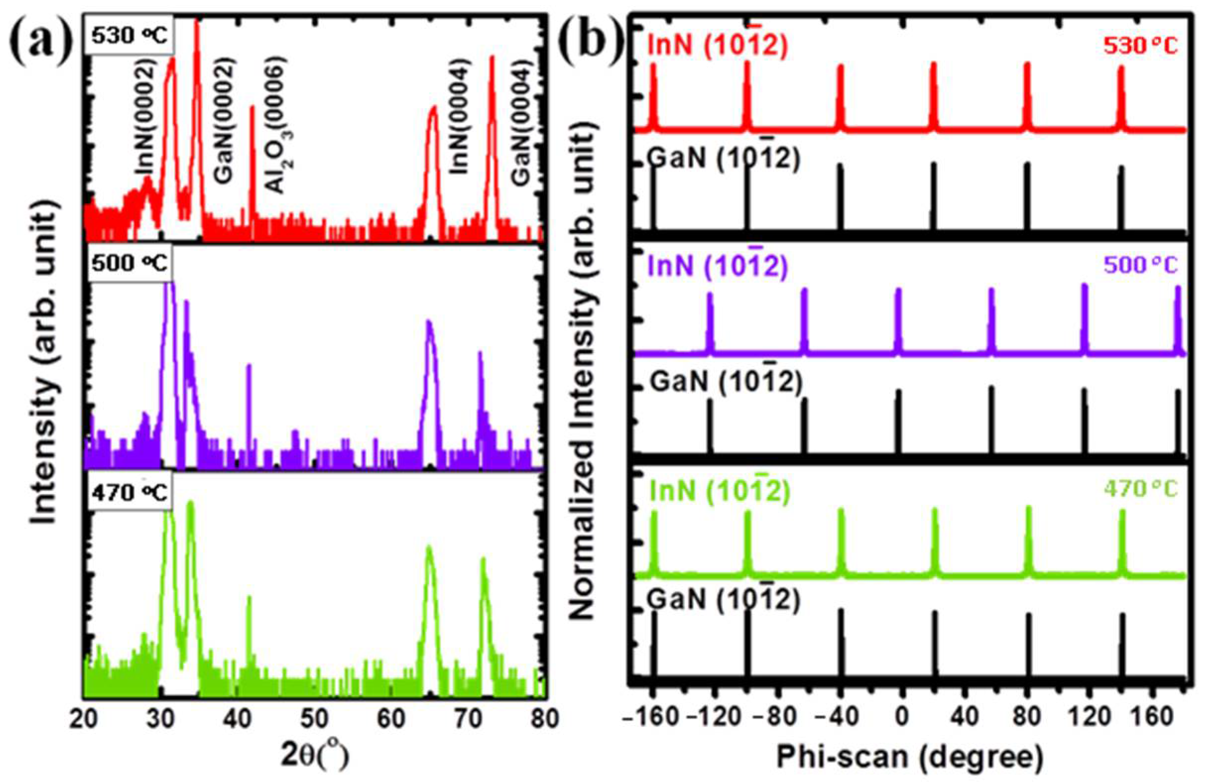
Figure 2a shows X-ray diffraction ω-2θ spectra for InN deposited directly on a GaN buffer layer, at various growth temperatures from 470 °C to 530 °C. There are five diffraction peaks detected, corresponding to: InN(0002), InN(0004) from wurtzite InN, GaN(0002), GaN(0004) from wurtzite GaN, and the (0006) diffraction from the sapphire substrate. However, no In metal peaks were detected in the patterns. These results indicate that InN films and nanorods with hexagonal structures are preferentially oriented and grown on a GaN template.
In order to determine the deposition relationship between InN and an underlying GaN template, the azimuthal ω-scan of the InN(
) and GaN(
) diffraction peaks were adopted. The in-plane orientations of the InN(
) are presented in
Figure 2b. The hexagonal structure of InN produced six equally spaced peaks, without any other random peaks, suggesting that the InN grew predominantly in the [0001] direction. Despite this, the 0° shift between InN and GaN reveals a coherent in-plane growth between the InN and GaN planes. These results indicate that InN films and nanorods were grown hetero-epitaxially on the GaN template with a hexagonal structure.
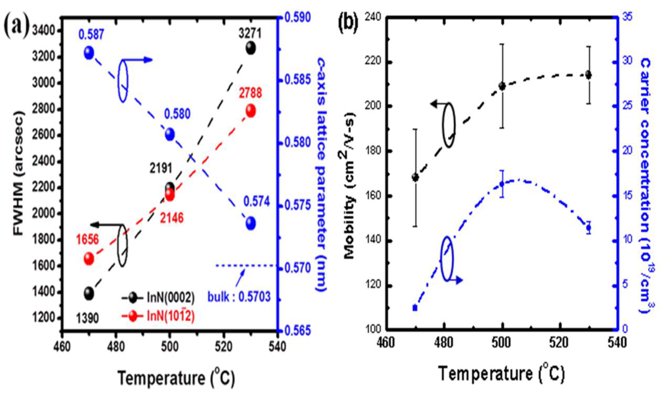
The right axis of
Figure 3 shows the c-axis lattice constant obtained from the InN films and nanorods that, utilizing the observed InN(0002) diffraction peak, is calculated to be larger than that of bulk InN (0.5703 nm). The c-axis lattice constant of InN obviously shifts closer to the bulk value as the growth temperature is increased. This implies that the nanorods produced may be under strain, and this stain relaxed while the InN films formed.
Due to the lattice and thermal expansion coefficient mismatch between the InN and the substrate, dislocations form in epilayers to release the strain as the critical thickness is reached. The high density of dislocations in hetero-epitaxial epilayers is described by the mosaic block model. Specifically, the out-of-plane rotation perpendicular to the surface normal is the mosaic tilt, and the in-plane rotation around the surface normal is the mosaic twist.
XRD rocking curves were measured for the InN(0002) and InN(
) reflections using ω-scanning geometry, in order to confirm the crystalline quality and calculate the density of dislocations in InN. The symmetric (0002)-reflecting plane is related to screw and mixed dislocations, and the asymmetric (
)-reflecting plane is directly influenced by edge dislocations. As show in
Figure 3a, the InN nanorods with a growth temperature of 470 °C have a greater crystalline quality in all InN samples, and the defects were apparently increased when the growth temperature and V/III ratio were increased. The following equation is used to estimate the dislocation density from the result of the XRD rocking curves [
28,
29,
30]:
where
Ddis is the dislocation density,
Dscrew is the compound dislocation density with screw and mixed dislocation,
Dedge is the compound dislocation density with edge and mixed dislocation,
β is the full width at half-maximum (FWHM) obtained from XRD rocking curves, and
b is the Burgers vector length. The calculated dislocation densities are shown in
Table 1. In the InN nanorods obtained with a growth temperature of 470 °C, the dislocation density was found to be 7.24 × 10
9 cm
−2, or a third of that obtained with a growth temperature of 530 °C. In the InN films, the crystalline structure removes the mismatch in the lattice and thermal expansion coefficients through the formation of dislocations, resulting in a higher dislocation density than with nanorods. This phenomenon will be discussed in the following paragraph.
Figure 3b shows the dependence of carrier concentration and mobility, as measured by the Hall effect. While the InN morphology changes from nanorods to films, the carrier concentration and mobility were found to be in the range 2.49 × 10
19 cm
−3, 1.63 × 10
20 cm
−3, 1.14 × 10
20 cm
−3; and 168, 209, 214 cm
2/V∙s. Hall measurements were not performed on a single InN nanorod in this experiment, which was expected to yield a very high mobility and low carrier concentration. Direct determination of the carrier concentrations by Hall measurement on a single nanorod is not easy in practice. The electrical properties of our InN samples were measured using a Hall-effect measurement system at room temperature. In addition, the In pellet is used as an ohmic contact. The purity of the pellet is 99.99%, and the diameter of the pellet is about 1 mm [
13,
14]. The InN nanorods have a lower carrier concentration and mobility than the InN films, which is due to the comparatively greater crystalline quality and 1D structure of the InN nanorods. Fabrication of dislocation-free InN nanorods on heterogeneous substrates has been successfully investigated in the literature [
26,
31]. Therefore, we might expect only a little deviation from ideal stoichiometry of the InN nanorods, resulting in lower carrier concentration and higher mobility than InN films. However, the impact of surface roughness and ingrain and grain boundary scattering limits the electron mobility. Therefore, the results of Hall measurement on the InN samples are more suitable as an indication for the tendency, rather than an absolute value. Since the nearly dislocation-free InN nanorods are formed in our experiments, the difference between the defect characteristics of 1D nanorods and 2D thin-film, as listed in
Table 1, will affect the electrical and optical properties of the InN material.
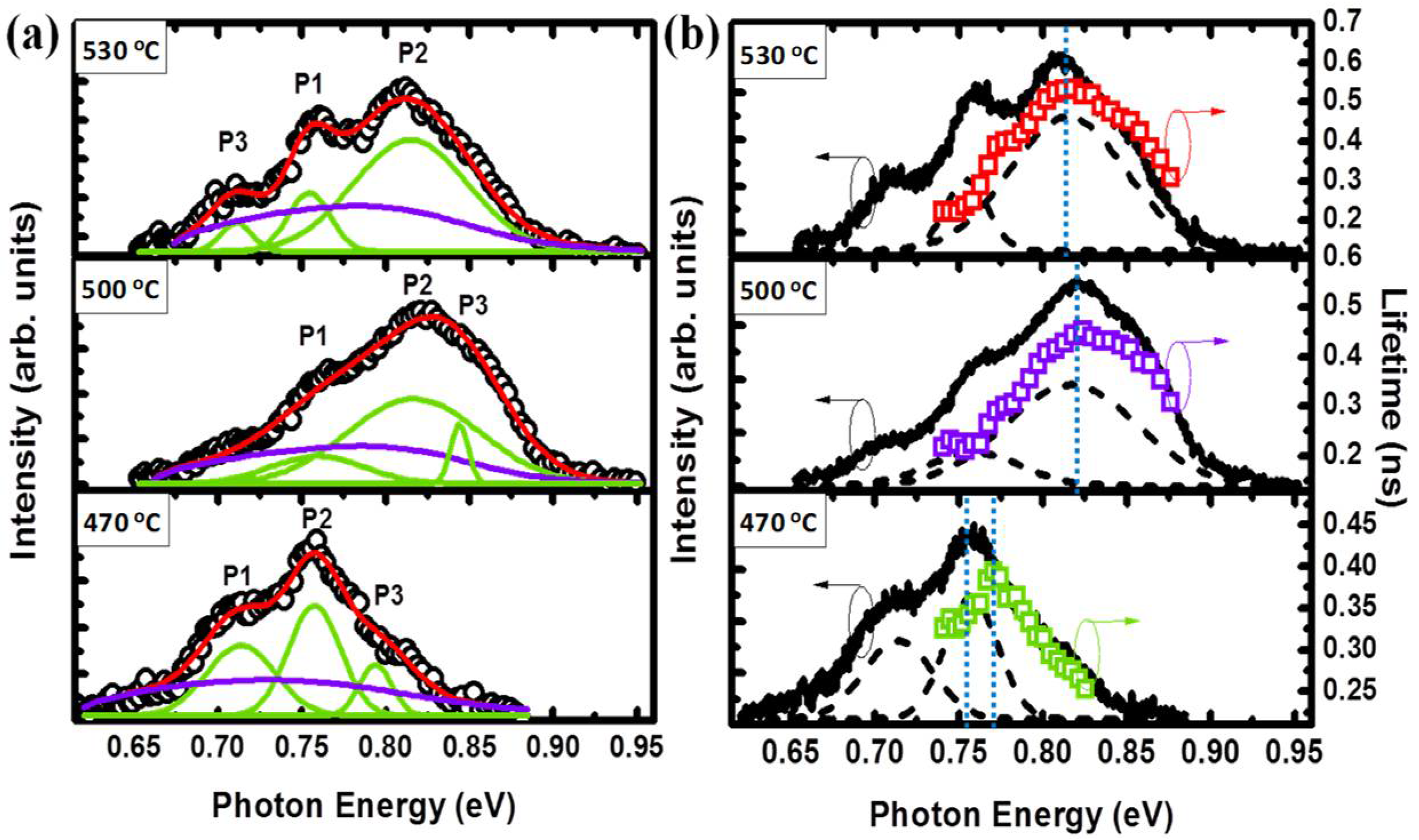
Figure 4a shows the low-temperature PL spectra of the InN samples, indicating that InN has dominant peaks with three kinds of recombination labeled as P1, P2, and P3. The emission spectrum exhibited a broadened feature with a higher carrier concentration, and the band-filling effect may dominate. This spectral feature is complex, and the emission peak is much greater than the accepted band gap (0.65–0.7 eV). Those high-energy peaks are generally attributed to degenerate electrons-to-band or -to-acceptor level [
31,
32]. However, the peaks with high energy showed a stronger luminescence than those with low energy. This phenomenon is unlikely to be explained by degenerate-to-band, because of the lack of high k-value holes in the valance band of degenerate
n-InN. Therefore, the peaks with high energy could originate from degenerate electrons-to-acceptors.
In the early literature, it was reported that high emission energy and high-intensity luminescence were interpreted using Mahan excitons [
33]. Mahan excitons can be described as localized holes of widespread
k that interact with electrons in the conduction band because the electrons are located on the Fermi edge. As the carrier scattering is enhanced, the optical transition matrix is extremely magnified, while the electrons below the Fermi energy level have only a weak recombination with the localized holes. Therefore, in the degenerate semiconductor, the high emission energy peaks show more intensive luminescence than that of the near-band edge types.
To further confirm the mechanism of carrier recombination, the low-temperature PL spectrum is fitted by an equation which assumes that the transition is due to free electron and acceptor recombination:
In Equation (2),
ћω is the photon energy,
Eg represents the band gap value,
EA is the energy of acceptor ionization energy,
EF represents the quasi-Fermi energy, and
kb and
T represent the Boltzman coefficient and electron temperature, respectively. During the fitting process, the Gaussian band was added to explain the enhanced effect of the Fermi edge singularity on the optical matrix of the Mahan excitons [
34]. The fitting line shape is plotted in
Figure 4a, which is in agreement with the experimental spectra, and a summary of the fitted results is provided in
Table 2.
These results show that two distinctly different acceptor levels participate in the recombination process (P1, P2 of all samples), and the Mahan exciton is represented by the strong luminescence intensity. According to the values obtained from fitting the results, the P3 of T
g = 470 °C and 500 °C InN samples is attributed to the free electrons at the Fermi edge recombining with the free hole (e, h), and the P3 of T
g = 530 °C InN samples is related to the near-band-edge recombination (NBE). The band gap energy of an InN nanorod is 0.65 eV, which reveals a greater crystalline quality when compared to InN films (0.70 eV, 0.71 eV). It is known that the structure and electronic properties of semiconductors can be altered by applying external stress or inducing internal strains through lattice and/or thermal mismatch strains in thin films [
35,
36,
37]. Interatomic distances and the relative positions of atoms have a strong bearing on the band structure and
Eg in compound semiconductors. Previous research on III-nitride has pointed out that the wurtzite bandgap of III-nitride can be modulated by uniaxial and/or biaxial strains. Dong et al. and Duan et al. have proposed that the reduction in the band gap may be accomplished for modest and realistic strains [
35,
36]. As shown in
Figure 3a of the manuscript, the degree of lattice relaxation is higher while increasing the growth temperature. Thus, the band gap energy of an InN nanorod may be slightly smaller than other InN films. Moreover, there is a small discrepancy between the theoretical line and experimental spectra at the lower energy side, which is attributable to the band tail states at the band edge that were neglected in Equation (2).
We used energy-dependent time-resolved photoluminescence (ED-TRPL) to further confirm the presence of Mahan excitons in these InN materials. Once Mahan excitons exist, the deep localized holes involved in the Mahan excitons can capture the carrier, preventing them from escaping from the localized states and prolonging lifetime. The results of the ED-TRPL in
Figure 4b show that a localized state does exist in the InN samples, in which lifetime can be fitted through the following single-exponential decay, such as Equation (3):
In Equation (3), I0 represents luminescence intensity at t = 0, and τ represents the carrier lifetime. The fitting results indicate that the peak position of longest lifetime coincides with the dominant peak (P2) for InN films (Tg = 500 °C and 530 °C). Except the main peaks, the ED-TRPL data presented no significant change on the left side, which matched the second strongest peak (P1) for all samples. This standstill of lifetime also indicated a localization of the phenomenon related to Mahan excitons, but was weaker than the main peak because of the shorter carrier lifetime. However, the longest lifetime in the InN nanorods was located at a higher energy level than the main peak, which was assigned as near Mahan exciton recombination. This result might be because of the obvious band-bending phenomenon in the nanorod structure surface, resulting in the longest blue-shift lifetime compared with the peaks for Mahan exciton recombination.
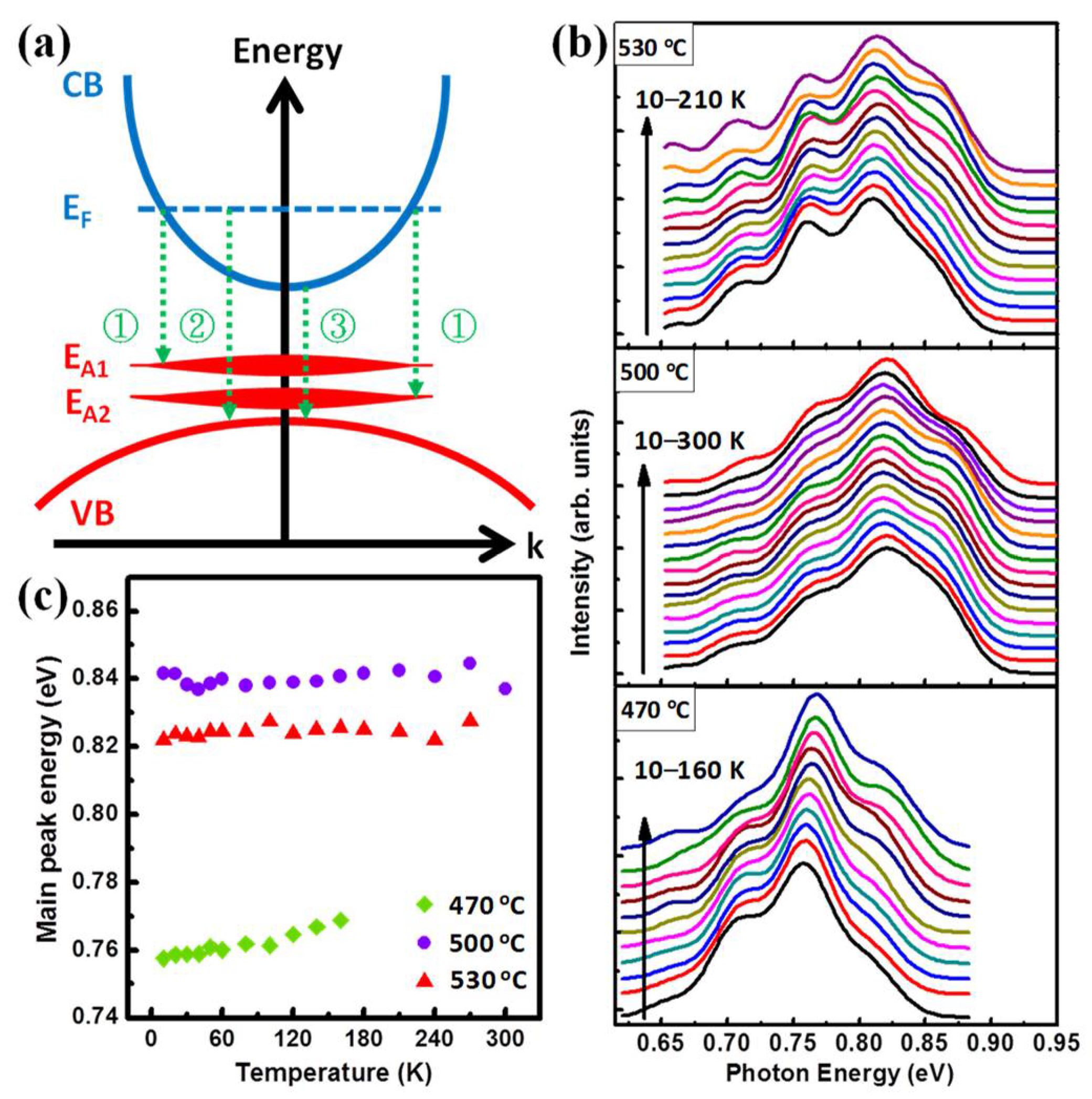
A schematic of the carrier recombination in the InN samples is shown in
Figure 5a. Transition 1 is Mahan exciton recombination with two different hole-localized acceptors with high k-values. Due to the widespread k of acceptor wave function, there was a strong luminescence intensity display due to the scattering rate being enhanced at the Fermi edge. Transitions 2 and 3 are Fermi-edge to valence-band recombination, and near-band-edge recombination with low k-value and Γ-point, respectively. The luminescence intensity of transitions 2 and 3 is weaker than transition 1 due to the small number of holes at the Fermi vector in the valence band and Γ-point.
Figure 5b shows the temperature-dependent PL spectra taken from samples with different structures. For the nanorod structure, the main peak shows a significant blue shift in
Figure 5c at all temperature ranges. However, the PL signal decreased more rapidly than was seen with the film type samples. The spectrum cannot be analyzed at temperatures over 160 K due to the low S/N ratio. The phenomenon of blueshift in the main peak can be ascribed to the band bending near the nanorod’s surface because of the electron accumulation layer. Compared with the film structure, the large surface-to-column ratio of the rod structure may cause a more significant band-bending phenomenon. The photo-induced holes tend to move from a low energy state at the rod center to a high energy state near the surface as the temperature increases, thus leading to an anomalous blue shift [
38]. The rapid decrease in luminescence intensity in the InN nanorods can also be attributed to the large surface-to-column ratio, which makes the influence of surface state more significant. The InN films show a strong luminescent characteristic even at high temperatures. The position of the peak in
Figure 5c shows that there is no significant shift in any of the temperature ranges. In this case, the 2D film-type InN sample has a very high carrier concentration. In such a highly degenerate
n-type InN semiconductor, the temperature-induced band gap shrinkage can be easily compensated by the increased electron Fermi level, so there is almost no peak shift [
11].
The hexagonal InN with a wurtzite structure was of the
space group, including four atoms in a unit cell. For the factor group analysis at the Γ point, theory predicts six optical modes as follows:
. These six phonon branches all belong to a Raman active mode, with the exception of the silent B
1 mode. In our room-temperature Raman measurement, the z direction was found to be parallel to the c-axis and the x and y directions were normal to z. According to the backscattering z(x,-)¯z geometry, only the E
2 and A
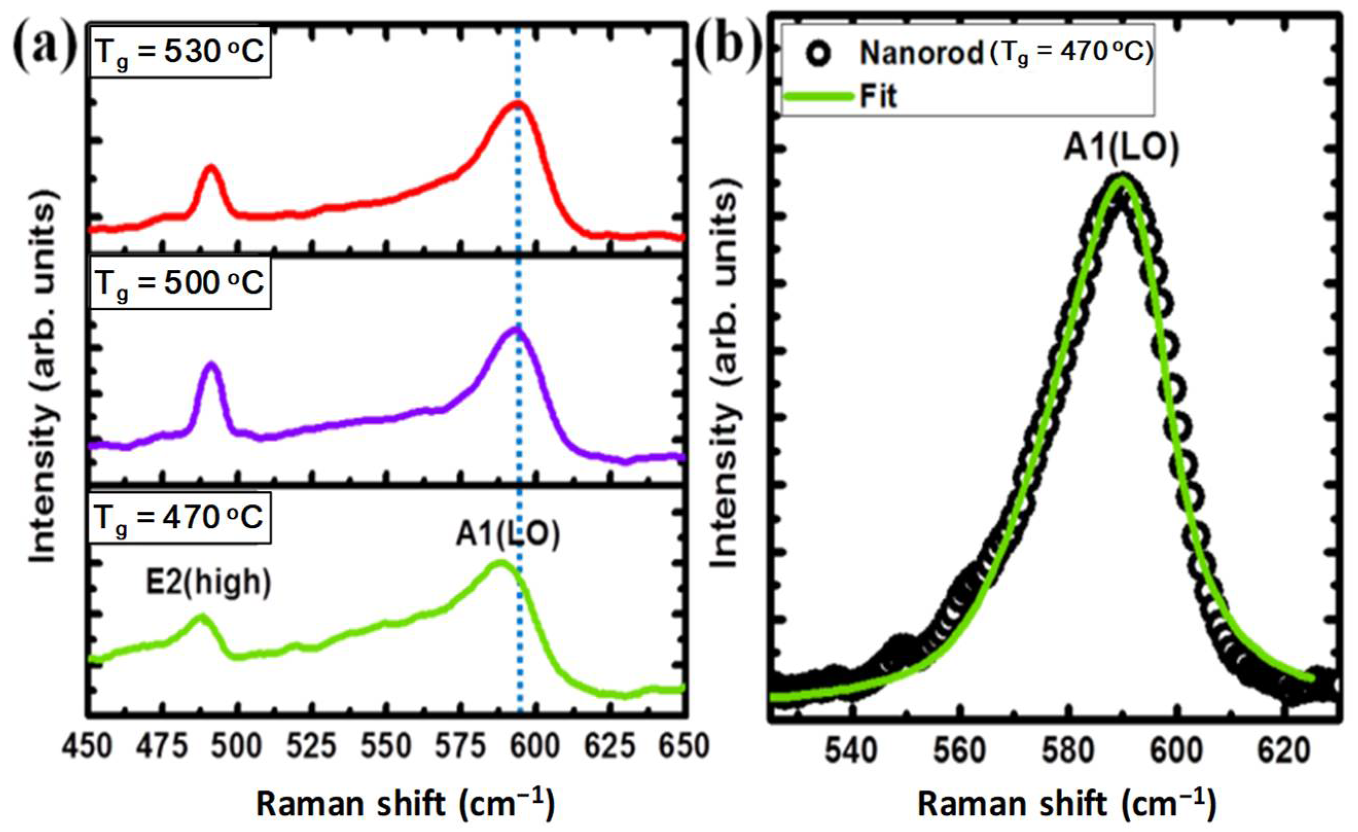
1(LO) modes are allowed by selection rules for the c-plane InN grown on the (0001) substrate. The Raman spectrum of the InN samples is displayed in
Figure 6a. There are two well-resolved active phonon modes of E
2(high) and A
1(LO), which are located at approximately 491 cm
−1 and 591 cm
−1, respectively. The asymmetric line shape of the A
1(LO) modes can be described by Fano interferences [
39], which occur between the zone-center LO phonons and the quasi-continuum electronic state along the c-axis. In the typical case of Fano interferences in Raman spectra, the peak of the A
1(LO) modes displays an asymmetrical broadening line width with an increased carrier concentration, due to the strong interaction between A
1(LO) phonons and the free carriers distributed in the in-plane of InN. It is worth noting that the A
1(LO) mode of InN nanorods exhibits a manifestly broad asymmetrical and frequency-downshifted line shape compared to the InN films, even though the carrier concentration of the InN nanorods is lower. This phenomenon implies that the A
1(LO) phonons are not solely influenced by carrier concentration.
Thus, the spatial correlation effect [
40,
41,
42] is introduced to describe the expression of A
1(LO) phonons for InN nanorods. The Raman intensity
I(ω) at a frequency ω can be expressed by the following integral, and we assume a spherical correlation region and Brillouin zone for simplicity:
where
q is expressed in units of 2π/a, a is the lattice constant,
L is the spatial correlation length,
ω(q) represents the phonon dispersion, and
Γ0 is the width of the intrinsic Raman line shape. A Gaussian spatial correlation function,
, leads upon Fourier transformation to an average over
q with a similar weighting factor
. This is used to account for
q-vector relaxation related to finite-size effects, and structural disorder. For the relation of phonon dispersion,
ω(q) is taken into consideration in a one-dimensional linear-chain model to approximately describe the dispersion:
Figure 6b demonstrates that the fitted curve is in agreement with the experimental Raman line shape of the A
1(LO) mode. From the fitting results by Equations (4) and (5), we obtain the parameters:
,
,
, and
L = 5 nm. This clearly shows that the phonons in nanorods are influenced by the spatial correlation effect. The asymmetric broadening of the Raman line width of the A
1(LO) phonon may be caused by the following: (i) disorders in the crystalline structure induce the mode correlation functions of the phonon to become finite, with the relaxation of the
q = 0 selection rule associated with finite correlation length; (ii) the phonons at the Brillouin zone edge participate in inelastic collision with photons. The asymmetric broadening at the low energy side and downshifted frequency of the Raman line shape is due to the energy of the Brillouin zone edge being lower than that of the Brillouin zone center.


 ,
, 


