Article

First-Principles Study of Electronic and Optical Properties of Two-Dimensional WSSe/BSe van der Waals Heterostructure with High Solar-to-Hydrogen Efficiency

1
School of Mechanical Engineering, Wanjiang University of Technology, Maanshan 243031, China
2
School of Mechanical and Electronic Engineering, Nanjing Forestry University, Nanjing 211189, China
3
School of Science, Jiangsu University of Science and Technology, Zhenjiang 212001, China
4
School of Automation and Information Engineering, Xi’an University of Technology, Xi’an 710048, China
5
School of Materials Science and Engineering, Southeast University, Nanjing 211189, China
*
Authors to whom correspondence should be addressed.
Submission received: 20 July 2021 / Revised: 15 August 2021 / Accepted: 17 August 2021 / Published: 18 August 2021

Abstract

:
In this paper, the optical and electronic properties of WSSe/BSe heterostructure are investigated by first-principles calculations. The most stable stacking pattern of the WSSe/BSe compounds is formed by van der Waals interaction with a thermal stability proved by ab initio molecular dynamics simulation. The WSSe/BSe heterostructure exhibits a type-I band alignment with direct bandgap of 2.151 eV, which can improve the effective recombination of photoexcited holes and electrons. Furthermore, the band alignment of the WSSe/BSe heterostructure can straddle the water redox potential at pH 0–8, and it has a wide absorption range for visible light. In particular, the solar-to-hydrogen efficiency of the WSSe/BSe heterostructure is obtained at as high as 44.9% at pH 4 and 5. All these investigations show that the WSSe/BSe heterostructure has potential application in photocatalysts to decompose water.

Graphical Abstract

1. Introduction

Since graphene was first prepared in 2004 [1], two-dimensional (2D) materials have attracted much attention due to their excellent electronic, optical, thermal and catalytic properties [2,3,4,5,6]. There are many kinds of elements in two-dimensional (2D) materials, including almost all of the elements [7]. One of most popular layered materials is transition metal dichalcogenides (TMDs), whose chemical composition is usually expressed by MX2, in which the M and X represent a transition metal (Ti, Ta, W, etc.) and chalcogen (S, Se, Te, etc.), respectively [8,9]. The monolayer TMD materials could be extensively applied for the study of nano-devices [10], photocatalysts [11] and optoelectronics [12] because of their novel electronic properties and a direct bandgap of 1.1–2.0 eV [13]. In addition, considering their high flexibility and carrier transport properties in the atomic layer, TMDs are ideal for applications in flexible substrates and suitable for flexible and portable electronic devices [9,14].
To extend the application range of 2D materials, recently, many new 2D materials have been predicted by the methods of global structure search and high throughput calculations [15,16]. For example, B2P6 was found to possess a Janus structure, which provides it with promising applications as a photocatalyst for water splitting and metal-ion batteries [17]. In addition, instead of a covalent bond [18], forming a 2D van der Waals (vdW) heterostructure is a common method to improve the properties of layered materials [19,20,21]. These weak vdW forces combine two different layered materials, which keep the heterostructure energetically stable [22,23]. The interface of a 2D heterostructure can create many interesting properties which enhance the electronic, optical and photocatalytic abilities [24,25,26]. Thus, a number of 2D materials have been built and used as p–n junctions [27], photocatalysts [28], field-effect transistors [29], etc. In detail, a vdW heterostructure with a sandwich structure based on MoS2−graphene−WSe2 was prepared by the mechanical exfoliation method possessing a wide absorption spectrum, which demonstrates that the heterostructure has a specific detectivity of up to 1011 Jones [30]. The graphene/MoS2 heterostructure was formed by chemical vapor deposition (CVD), and the heterostructure was used in high-performance devices and circuits, with MoS2 and graphene acting as the transistor channel and contact electrodes, respectively. Importantly, the novel electronic and optical properties of 2D heterostructures also can been tuned by electric fields [31], external biaxial strain [32], defects [33], etc. The above reports show that vdW heterostructures can be used as candidates for high-performance nano-electronic and optoelectronic devices.
Recently, the TMD materials with a Janus structure have widely been investigated, since the MoSSe was grown using a synthetic strategy with vertical dipoles [34]. Then, the Raman vibrational modes and electronic structures of the Janus MoSSe monolayer were calculated by means of density functional theory (DFT) and compared with the corresponding experimental results. It was found that Janus monolayers have high activity of hydrogen evolution on the base surface. Density functional calculation shows that the activity comes from the mutual effect of structural strain and inherent defects of Janus MoSSe [35]. Similarly, the Janus WSSe monolayer also has superior carrier mobility of about 600 cm2·V1·s1, which is more advantageous than conventional TMD monolayers and other Janus TMD materials [36]. Considering the pronounced electronic and optical properties of the WSSe monolayer, it has been constructed as a heterostructure with MoSSe and possesses intrinsic many-body effects. Both horizontal and vertical WSSe/MoSSe heterostructures have type-II band alignment [37]. More recently, a boron selenide (BSe) monolayer was studied as a semiconductor with an indirect bandgap [38]. Furthermore, BSe-based heterostructures are also addressed by g-GaN/BSe [23], ZnO/BSe [24], blue phosphorene/BSe [39], etc., which shows the promising applications for BSe-based heterostructures in electronics, spintronics, and optoelectronics.
In this paper, based on DFT, some interesting properties of the WSSe and BSe monolayers and the WSSe/BSe heterostructure are addressed. The WSSe/BSe heterostructure is decided by the stacking structure with lowest binding energy, and the thermal stability of the WSSe/BSe heterostructure is examined. Then, the interfacial properties of the WSSe/BSe heterostructure are investigated according to the potential drop and charge density difference. The optical absorption property and optical conversion efficiency of the WSSe/BSe heterostructure are also studied. Our research can provide effective guidance for the application of such vdW heterostructures in future nano-electronic and optoelectronic devices.

2. Computing Method

Based on density functional theory (DFT), first-principles calculations were conducted using the Vienna ab initio simulation package (VASP) [40,41]. The projector-augmented wave method with energy cutoff of 550 eV was considered. The generalized gradient approximation (GGA) [42] of Perdew–Burke–Ernzerhof functional (PBE) was used to explain the electron exchange and correlation potential [43,44,45]. For the accurate electronic and optical properties, the Heyd–Scuseria–Ernzerhof (HSE06) method was utilized [46]. The Grimme correction method (DFT-D3) was explored to describe the weak dispersion for the vdW correction [47]. In the first Brillouin zone, 11 × 11 × 1 k-point mesh was employed. The vacuum thickness of 25 Å was considered to prevent the interaction of nearby layers. In addition, the convergence criteria of total energy and the Hellmann−Feynman forces for the atoms of the system investigated in this work were 1 × 10⁻⁵ eV and 0.01 eV·Å−1, respectively. Furthermore, we built the model of monolayered WSSe, BSe and the WSSe/BSe heterostructure with the initial lattice constants of 3.23, 3.25 and 3.24 Å, respectively [48,49]. Then, we relaxed all of the systems and obtained the appropriate lattice constants.

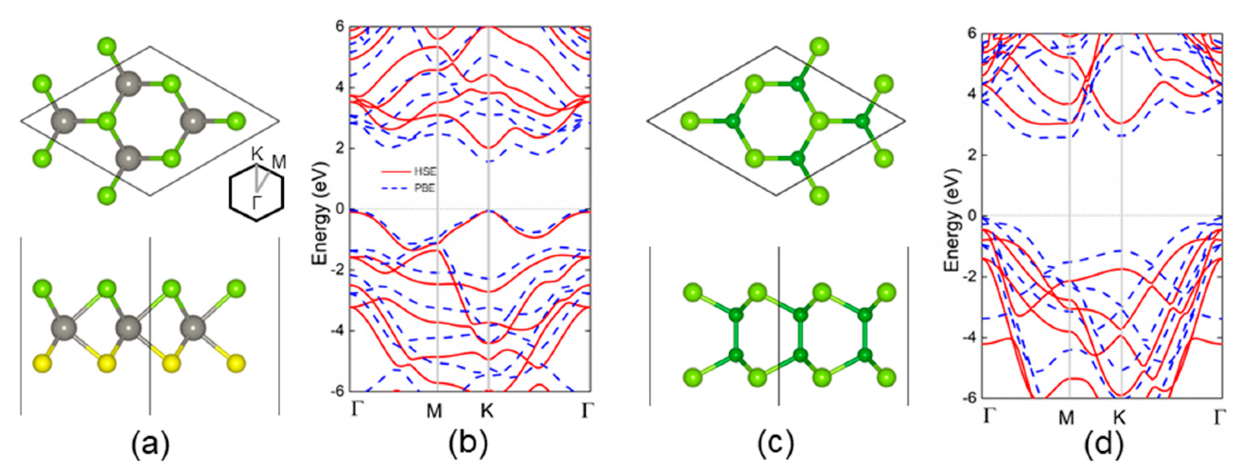
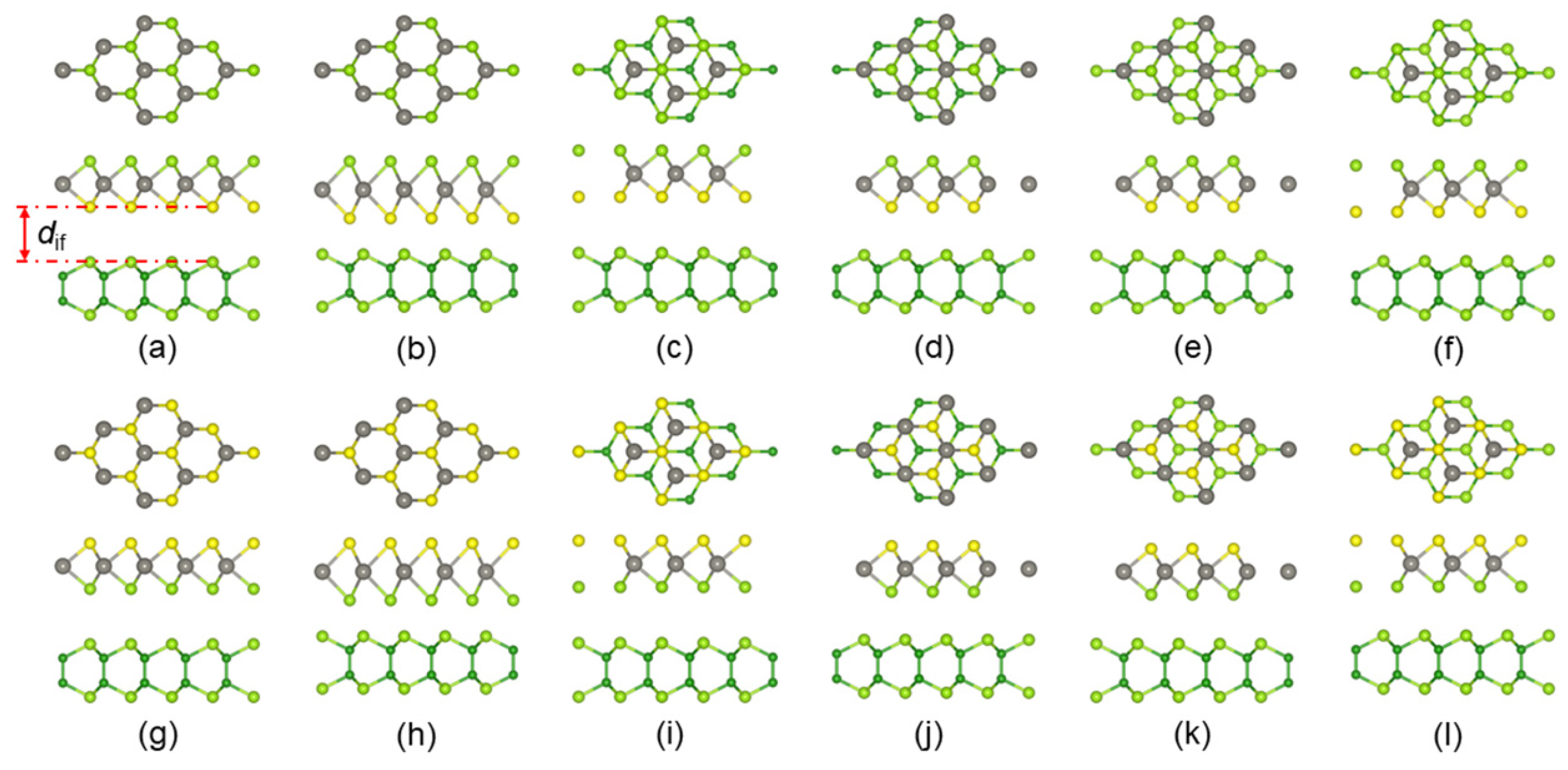
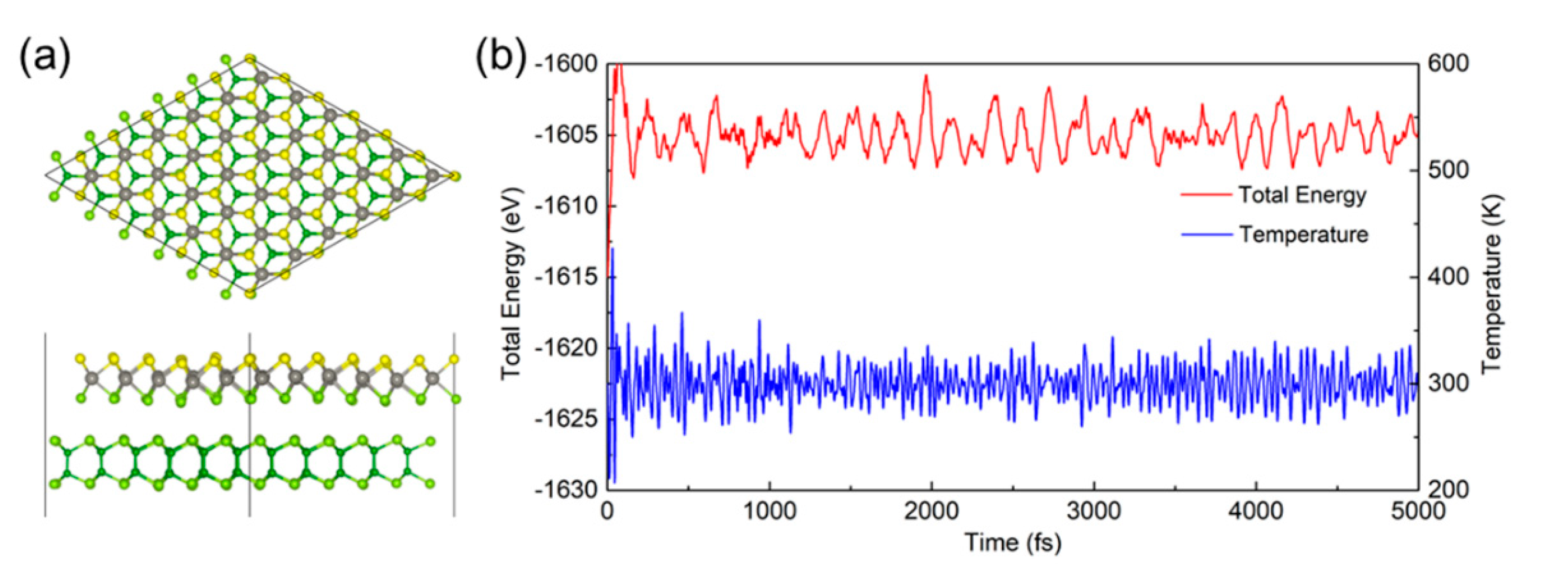
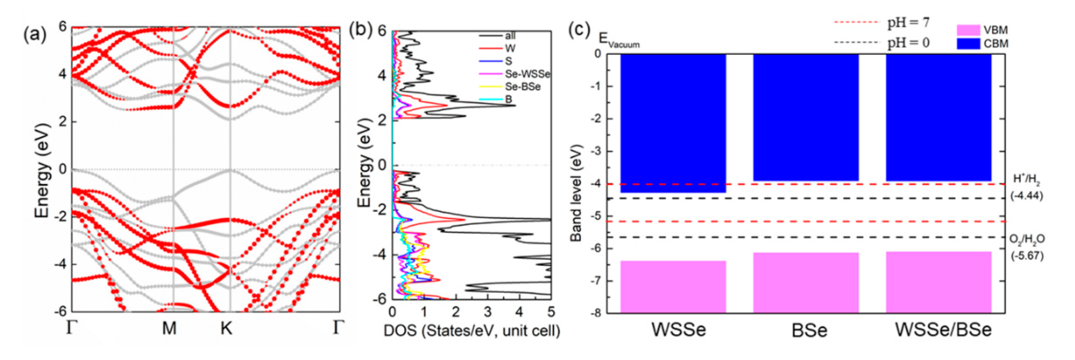
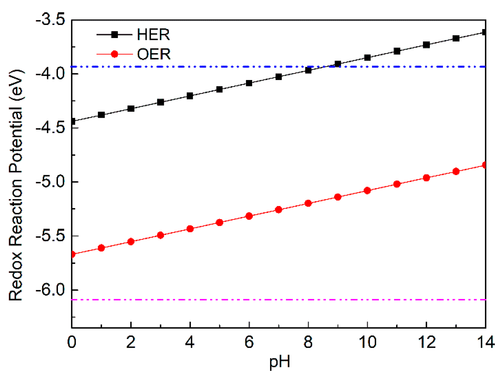
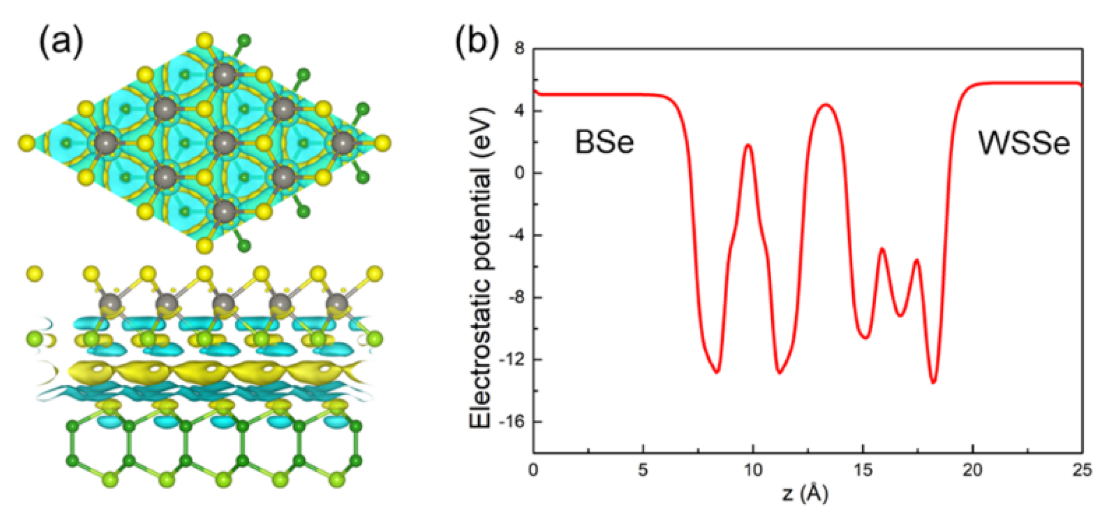
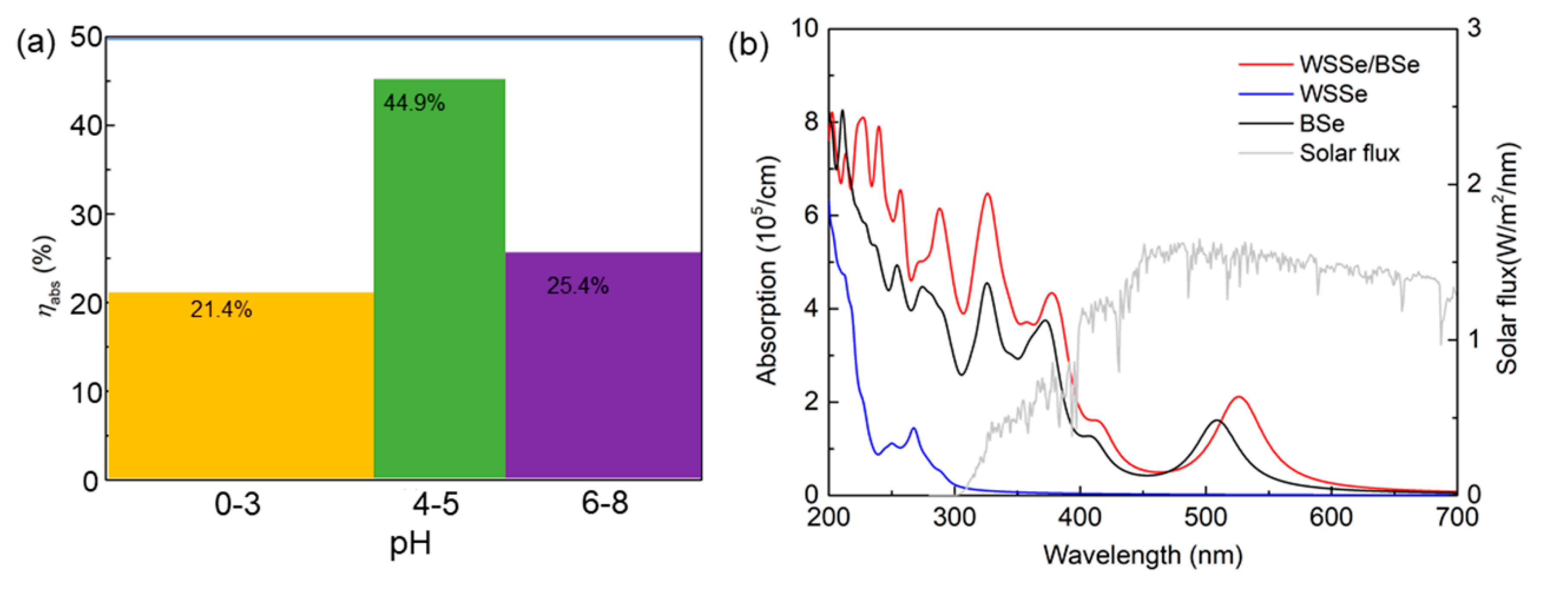
3. Results and Discussion

First, the structures were optimized for the pristine WSSe and BSe monolayers shown in Figure 1a,c, respectively, at 3.269 and 3.245 Å for lattice constants. The bond lengths of the W–S, W–Se and B–Se in the monolayered WSSe and BSe were obtained as 2.428, 2.542 and 2.099 Å, respectively. Furthermore, using HSE06 calculations and the PBE method, the band structures of both monolayered materials are calculated in Figure 1a,b, and one can find that the WSSe has a direct bandgap of 2.077 eV (HSE results) with the conduction band minimum (CBM) and the valence band maximum (VBM) located at the K points, while the BSe possesses an indirect bandgap of 3.466 eV. The CBM of the BSe appears at the point M, while the VBM is located at the Γ point. In addition, all these findings are consistent with previous reports [50,51], which proves that our computational methods are accurate and reliable.
Next, we constructed the heterostructure composed by WSSe and BSe monolayers. As the lattice parameters of the WSSe and BSe monolayers shows very small lattice mismatch (about 0.74%), they are suitable to be designed as a heterostructure, which can induce a precise stacking configuration. Here, we considered 12 possible highly symmetric stacking patterns for the WSSe/BSe heterostructure, as presented in Figure 2. γ-1, γ-2, γ-3, γ-4, γ-5 and γ-6 stacking are similar with γ-7, γ-8, γ-9, γ-10, γ-11 and γ-12 stacking, respectively, by exchanging the site of the S and Se atoms in the WSSe layer. For γ-1, W and Se (or S) atoms are put on top of B atoms and Se atoms, respectively. The γ-2 style is obtained by changing the positions of B and Se atoms from the γ-1 configuration. Meanwhile, for γ-3, W atoms are positioned on top of the hexagonal center of the BSe, and Se (or S) atoms are located on top of Se atoms in BSe layer. γ-4 can be constructed by locating the Se (or S) atoms on the top of the hexagonal center of BSe and W atoms on the top of the Se atoms in the BSe layer. For the γ-5 style, Se (or S) atoms are positioned on the top of the hexagonal center of BSe, and W atoms are located on the top of B atoms. γ-6 is built by changing the positions of W and Se (or S) fromm γ-5.
For all those representative highly symmetric stacking patterns, we judged the most stable one by calculating the binding energy (Eb) as follows:
Eb = (EWSSe-BSeEWSSeEBSe)/A
where EWSSe/BSe, EWSSe and EBSe are the energy of the WSSe/BSe heterostructure and the original WSSe and BSe monolayers, respectively. A is the area of the cell. The obtained Eb and interface distance (dif) are addressed in Table 1. The γ-10 stacking patterns possesses the lowest binding energy of −25.444 meV/Å−2, which is smaller than that in the vdW bonding in weak interlayer interactions in graphites of about −18 meV/Å−2, demonstrating that the WSSe/BSe heterostructure is formed by vdW interactions [52]. In addition, the bond lengths of the W–S, W–Se and B–Se in the monolayered WSSe and BSe only show a slight change in the heterostructure, which further explains the weak vdW interactions between the interface of the heterostructure. Therefore, all of the following investigations are focused on the γ-10 stacking configuration.
Then, we evaluated the thermal stability of the WSSe/BSe vdW heterostructure by ab initio molecular dynamics (AIMD) simulation with a Nosé–Hoover heat bath scheme [53]. In this simulation, due to the lattice translation constraint, we built a 6 × 6 × 1 supercell for the WSSe/BSe vdW heterostructure including 252 atoms. After completing the simulation calculations, as shown in Figure 3a, the WSSe/BSe vdW heterostructures were still integral after 5 ps at 300 K, demonstrating their pronounced thermal stability at room temperature. Moreover, with the simulation step, the change in the total energy of the WSSe/BSe vdW heterostructure and the fluctuation in temperature are shown in Figure 3b, which demonstrates a convergence with the simulation. It is worth noting that the γ-8 WSSe/BSe vdW heterostructure shows little difference in the binding energy (about 0.111 meV/Å−2) compared with the γ-10 WSSe/BSe vdW heterostructure, and so the thermal stability of the γ-8 WSSe/BSe vdW heterostructure was also addressed in Supplementary Figure S1, in the Supporting Information, which suggests that the γ-8 WSSe/BSe vdW heterostructure possesses a thermal stability at room temperature.
We also calculated the projected band structure for the WSSe/BSe vdW heterostructure, shown in Figure 4a, obtained by using HSE06 calculations. We found that the WSSe/BSe vdW heterostructure has a direct bandgap of 2.151 eV, which means that it is a semiconductor. It is interesting that both the VBM and CBM of the heterostructure are donated from the WSSe layer, exhibiting a type-I band alignment, as shown in Figure 4a. Furthermore, we calculated the projected density of states of the WSSe/BSe vdW heterostructure shown in Figure 4b, which can further prove the type-I band alignment in the WSSe/BSe vdW heterostructure. Previous studies have shown that a potential photocatalyst should possess decent electronic characteristics, which can be used to decompose water [54]. Firstly, the band gap should be between 1.23 and 3.0 eV. Secondly, the band edge positions of the photocatalyst should meet the water redox potentials, which means that the potential of the VBM should be lower than −5.67 eV and the potential of the CBM of materials should be higher than −4.44 eV [39]. The calculated bandgap (2.151 eV) of the WSSe/BSe vdW heterostructure reveals the suitable bandgap value as a photocatalyst to decompose water [12], and the band edge positions of the monolayered WSSe, BSe and WSSe/BSe vdW heterostructure are calculated in Figure 4c, showing that the band alignments of these layered materials all possess decent potential for the oxidation and reduction reactions to decompose water at pH 0.
Considering the influence of the pH value, the reduction and oxidation potentials are obtained from the value of the pH as: Ereduction = −4.44 eV + pH × 0.059 eV, and Eoxidation = −5.67 eV + pH × 0.059 eV, respectively [55]. As shown in Figure 4c, the band alignment of the WSSe/BSe vdW heterostructure still possesses decent band edge position energy level for the water redox potentials at pH 7, but the WSSe monolayer is not suitable for the photocatalyst for the hydrogen evolution reaction (HER). Furthermore, we investigated the potentials of the oxygen evolution reactions (OER) and HER to decompose water at different pH compared with the band edge energy of the WSSe/BSe vdW heterostructure in Figure 5, showing that the WSSe/BSe vdW heterostructure still can induce the OER and HER at pH 0 to 8 to decompose the water.
As for the interfacial properties of the vdW heterostructure in this work, the charge density differences (Δρ) were investigated by:
Δρ = ρWSSe/BSeρWSSeρBSe
where ρWSSe/BSe, ρWSSe and ρBSe mean the charge density difference of the WSSe/BSe heterostructure and the isolated WSSe and BSe layers, respectively. As shown as Figure 6a, the cyan regions represent the negative values of chargers, and the yellow regions represent the positive values, which shows that the charge redistribution is mainly around the interface of the WSSe/BSe vdW heterostructure. In addition, the Bader charge analysis method [56,57] was used to calculate the charge transfer between the WSSe and BSe layers. We found that there are only 0.0047 transferred electrons from the BSe layer to WSSe layer. Moreover, the electrostatic potential drop across the interface of the WSSe/BSe vdW heterostructure is calculated in Figure 6b, which indicates that the WSSe layers present a slightly lower potential than the BSe layers in their corresponding heterostructure. This contributes to the formation of a built-in electric field, which is also an important factor for carrier migration.
We further investigated the optical properties of the WSSe/BSe vdW heterostructure. The solar-to-hydrogen (STH) efficiency is critical, which is also influenced by the pH values. The efficiency of the STH (ηSTH) is decided by:
ηSTH = ηabs × ηcu
where ηabs and ηcu are called the efficiency of light absorption and carrier utilization, respectively. Additionally, the ηabs is calculated as:
η abs = E g P ( h ω ) d ( h ω ) 0 P ( h ω ) d ( h ω )
in which the P() is demonstrated for the solar energy flux of AM1.5G by the energy of for phonon, and where Eg is used for the bandgap of the heterostructure. The ηcu is obtained by:
η cu = Δ G E P ( h ω ) h ω d ( h ω ) E g P ( h ω ) d ( h ω )
where the potential difference is described by ΔG, which explains water splitting of 1.23 eV. E is the energy of the phonon in water splitting, calculated by:
E = { E g , ( χ ( H 2 ) 0.2 , χ ( O 2 ) 0.6 ) E g + 0.2 χ ( H 2 ) , ( χ ( H 2 ) < 0.2 , χ ( O 2 ) 0.6 ) E g + 0.6 χ ( O 2 ) , ( χ ( H 2 ) 0.2 , χ ( O 2 ) < 0.6 ) E g + 0.8 χ ( H 2 ) χ ( O 2 ) , ( χ ( H 2 ) < 0.2 , χ ( O 2 ) < 0.6 )
where the overpotential of HER and OER are addressed by χ(H2) and χ(O2), respectively. Generally, 0.2 and 0.6 eV are suggested to be the required overpotentials for the HER and OER, as reported by a previous experimental study [58]. We calculated the ηSTH of the WSSe/BSe vdW heterostructure at different pH values, as shown in Figure 7a. The WSSe/BSe vdW heterostructure possesses a novel solar-to-hydrogen efficiency at pH 4 or 5, of about 44.9%, which is higher than that for other 2D heterostructures, such as PtS2/arsenene [59], arsenene/GaS and arsenene/GaSe [22]. In addition, the WSSe/BSe vdW heterostructure also possesses decent solar-to-hydrogen efficiency, of about 21.4% and 25.4% at pH 0–3 and pH 6–8, respectively.
The WSSe/BSe vdW heterostructure’s ability to absorb light is also obtained by:
α ( ω ) = 2 ω c { [ ε 1 2 ( ω ) + ε 2 2 ( ω ) ] 1 / 2 ε 1 ( ω ) } 1 / 2
where ε 1 ( ω ) represents the real parts of the dielectric constant, and ε 2 ( ω ) represents the imaginary parts, as shown as Figure 7b. The peaks of optical absorption for the WSSe, BSe and the WSSe/BSe vdW heterostructure are 2.11 × 10⁵, 1.44 × 10⁵ and 1.61 × 105 cm−1, located at the wavelengths of 523, 511 and 266 nm, respectively, which means that the WSSe monolayer and the WSSe/BSe vdW heterostructure possess novel optical absorption properties in the visible-light region. However, the WSSe does not have decent redox potential of HER for water splitting; thus, the WSSe/BSe vdW heterostructure is more suitable for use as a photocatalyst for water splitting.

4. Conclusions

In conclusion, we have systematically investigated some interesting features of the 2D WSSe, BSe and WSSe/BSe heterostructure by means of first-principles calculation. Our results demonstrate that the WSSe/BSe heterostructure can be constructed by vdW forces with thermal stability. Furthermore, the WSSe/BSe vdW heterostructure preserves the semiconductor feature of the original layered materials with a direct bandgap of 2.151 eV, and exhibits type-I band alignment. Furthermore, the WSSe, BSe and WSSe/BSe vdW heterostructure possess decent band edge positions to induce the HER and OER for water splitting at pH 0, while the WSSe/BSe vdW heterostructure still has excellent potential for redox reactions, decomposing the water at a pH value of 0–8. Furthermore, the WSSe/BSe vdW heterostructure can exhibit a novel STH efficiency, of up to about 44.9%, and a broader visible-light absorption range. All these findings demonstrate that the WSSe/BSe vdW heterostructure could be used as a potential photocatalyst to decompose water, and is a potential candidate for use in high-performance nano-electronic and optoelectronic devices.

Supplementary Materials

The following are available online at https://0-www-mdpi-com.brum.beds.ac.uk/article/10.3390/catal11080991/s1, Figure S1: The AIMD snapshots for WSSe/BSe vdW heterostructure with γ-8 stacking style; the total energy and temperature fluctuations during AIMD simulations for WSSe/BSe heterostructure with γ-8 stacking style.

Author Contributions

Conceptualization, Z.Z. and K.R.; methodology, K.R.; software, J.Y.; validation, Z.Z. and K.R.; formal analysis, K.R.; investigation, Y.X.; resources, K.R.; data curation, K.R.; writing—original draft preparation, Z.Z.; writing—review and editing, H.S.; visualization, Z.C.; supervision, K.R.; project administration, Z.Z.; funding acquisition, Z.H. All authors have read and agreed to the published version of the manuscript.

Funding

This work was supported by the Open Fund Project of Maanshan Engineering Technology Research Center of Advanced Design for Automotive Stamping Dies (Grant number: QMSG202003 and QMSG202105), the National Natural Science Foundation of Natural Science Basic Research Plan in Shaanxi Province of China (No.2021JM-345), China Postdoctoral Science Foundation (No.2020M683684XB).

Conflicts of Interest

There are no conflict to declare.

References

  1. Geim, A.K.; Novoselov, K.S. The rise of graphene. Nat. Mater. 2007, 6, 183–191. [Google Scholar] [CrossRef] [PubMed]
  2. Miro, P.; Audiffred, M.; Heine, T. An atlas of two-dimensional materials. Chem. Soc. Rev. 2014, 43, 6537–6554. [Google Scholar] [CrossRef] [PubMed]
  3. Li, L.; Han, W.; Pi, L.; Niu, P.; Han, J.; Wang, C.; Su, B.; Li, H.; Xiong, J.; Bando, Y. Emerging in-plane anisotropic two-dimensional materials. Info Mat. 2019, 1, 54–73. [Google Scholar] [CrossRef]
  4. Sun, M.; Luo, Y.; Yan, Y.; Schwingenschlögl, U. Ultrahigh Carrier Mobility in the Two-Dimensional Semiconductors B8Si4, B8Ge4, and B8Sn4. Chem. Mater. 2021. [Google Scholar] [CrossRef]
  5. Ren, K.; Liu, X.; Chen, S.; Cheng, Y.; Tang, W.; Zhang, G. Remarkable reduction of interfacial thermal resistance in nanophononic heterostructures. Adv. Funct. Mater. 2020, 30, 2004003. [Google Scholar] [CrossRef]
  6. Zheng, Z.; Ren, K.; Huang, Z.; Zhu, Z.; Wang, K.; Shen, Z.; Yu, J. Remarkably improved curie temperature for two-dimensional CrI3 by gas molecular adsorption: A dft study. Semicond. Sci. Technol. 2021, 36, 075015. [Google Scholar] [CrossRef]
  7. Butler, S.Z.; Hollen, S.M.; Cao, L.; Cui, Y.; Gupta, J.A.; Gutiérrez, H.R.; Heinz, T.F.; Hong, S.S.; Huang, J.; Ismach, A.F. Progress, challenges, and opportunities in two-dimensional materials beyond graphene. ACS Nano 2013, 7, 2898–2926. [Google Scholar] [CrossRef]
  8. Ren, K.; Sun, M.; Luo, Y.; Wang, S.; Yu, J.; Tang, W. First-principle study of electronic and optical properties of two-dimensional materials-based heterostructures based on transition metal dichalcogenides and boron phosphide. Appl. Surf. Sci. 2019, 476, 70–75. [Google Scholar] [CrossRef]
  9. Zhang, H.; Chhowalla, M.; Liu, Z. 2d nanomaterials: Graphene and transition metal dichalcogenides. Chem. Soc. Rev. 2018, 47, 3015–3017. [Google Scholar] [CrossRef]
  10. Radisavljevic, B.; Radenovic, A.; Brivio, J.; Giacometti, V.; Kis, A. Single-layer MoS2 transistors. Nat. Nanotechnol. 2011, 6, 147–150. [Google Scholar] [CrossRef]
  11. Kaplan, D.; Gong, Y.; Mills, K.; Swaminathan, V.; Ajayan, P.M.; Shirodkar, S.; Kaxiras, E. Excitation intensity dependence of photoluminescence from monolayers of MoS2 and WS2/MoS2 heterostructures. 2D Mater. 2016, 3, 015005. [Google Scholar] [CrossRef]
  12. Ren, K.; Wang, K.; Cheng, Y.; Tang, W.; Zhang, G. Two-dimensional heterostructures for photocatalytic water splitting: A review of recent progress. Nano Futures 2020, 4, 032006. [Google Scholar] [CrossRef]
  13. Mak, K.F.; Lee, C.; Hone, J.; Shan, J.; Heinz, T.F. Atomically thin MoS2: A new direct-gap semiconductor. Phys. Rev. Lett. 2010, 105, 136805. [Google Scholar] [CrossRef] [Green Version]
  14. Hong, X.; Kim, J.; Shi, S.F.; Zhang, Y.; Jin, C.; Sun, Y.; Tongay, S.; Wu, J.; Zhang, Y.; Wang, F. Ultrafast charge transfer in atomically thin MoS2/WS2 heterostructures. Nat. Nanotechnol. 2014, 9, 682–686. [Google Scholar] [CrossRef] [Green Version]
  15. Sun, M.; Schwingenschlögl, U. Structure prototype outperforming mxenes in stability and performance in metal-ion batteries: A high throughput study. Adv. Energy Mater. 2021, 11, 2003633. [Google Scholar] [CrossRef]
  16. Sun, M.; Yan, Y.; Schwingenschlögl, U. Beryllene: A promising anode material for Na-and K-ion batteries with ultrafast charge/discharge and high specific capacity. J. Phys. Chem. Lett. 2020, 11, 9051–9056. [Google Scholar] [CrossRef]
  17. Sun, M.; Schwingenschlögl, U. B2P6: A two-dimensional anisotropic janus material with potential in photocatalytic water splitting and metal-ion batteries. Chem. Mater. 2020, 32, 4795–4800. [Google Scholar] [CrossRef]
  18. Novoselov, K.S.; Mishchenko, A.; Carvalho, A.; Castro Neto, A.H. 2D materials and van der waals heterostructures. Science 2016, 353, aac9439. [Google Scholar] [CrossRef] [PubMed] [Green Version]
  19. Duong, D.L.; Yun, S.J.; Lee, Y.H. Van der waals layered materials: Opportunities and challenges. ACS Nano 2017, 11, 11803–11830. [Google Scholar] [CrossRef] [PubMed]
  20. Liu, Y.; Weiss, N.O.; Duan, X.; Cheng, H.-C.; Huang, Y.; Duan, X. Van der waals heterostructures and devices. Nat. Rev. Mater. 2016, 1, 16042. [Google Scholar] [CrossRef]
  21. Ren, K.; Wang, S.; Luo, Y.; Chou, J.-P.; Yu, J.; Tang, W.; Sun, M. High-efficiency photocatalyst for water splitting: A janus MoSSe/XN (X  =  Ga, Al) van der waals heterostructure. J. Phys. Phys. D Appl. Phys. 2020, 53, 185504. [Google Scholar] [CrossRef]
  22. Li, J.; Huang, Z.; Ke, W.; Yu, J.; Ren, K.; Dong, Z. High solar-to-hydrogen efficiency in Arsenene/GaX (X = S, Se) van der waals heterostructure for photocatalytic water splitting. J. Alloys Compd. 2021, 866, 158774. [Google Scholar] [CrossRef]
  23. Ren, K.; Luo, Y.; Wang, S.; Chou, J.-P.; Yu, J.; Tang, W.; Sun, M. A van der waals heterostructure based on graphene-like gallium nitride and boron selenide: A high-efficiency photocatalyst for water splitting. ACS Omega 2019, 4, 21689–21697. [Google Scholar] [CrossRef] [PubMed] [Green Version]
  24. Ren, K.; Yu, J.; Tang, W. Two-dimensional ZnO/BSe van der waals heterostructure used as a promising photocatalyst for water splitting: A dft study. J. Alloys Compd. 2020, 812, 152049. [Google Scholar] [CrossRef]
  25. Ren, K.; Yu, J.; Tang, W. A two-dimensional vertical van der waals heterostructure based on g-Gan and Mg(OH)2 used as a promising photocatalyst for water splitting: A first-principles calculation. J. Appl. Phys. 2019, 126, 065701. [Google Scholar] [CrossRef]
  26. Luo, Y.; Wang, S.; Shu, H.; Chou, J.-P.; Ren, K.; Yu, J.; Sun, M. A MoSSe/blue phosphorene vdw heterostructure with energy conversion efficiency of 19.9% for photocatalytic water splitting. Semicond. Sci. Technol. 2020, 35, 125008. [Google Scholar] [CrossRef]
  27. Lee, C.H.; Lee, G.H.; van der Zande, A.M.; Chen, W.; Li, Y.; Han, M.; Cui, X.; Arefe, G.; Nuckolls, C.; Heinz, T.F.; et al. Atomically thin p-n junctions with van der waals heterointerfaces. Nat. Nanotechnol. 2014, 9, 676–681. [Google Scholar] [CrossRef] [Green Version]
  28. Meng, R.; Jiang, J.; Liang, Q.; Yang, Q.; Tan, C.; Sun, X.; Chen, X. Design of graphene-like gallium nitride and WS2/WSe2 nanocomposites for photocatalyst applications. Sci. China. Mater. 2016, 59, 1027–1036. [Google Scholar] [CrossRef] [Green Version]
  29. Roy, T.; Tosun, M.; Kang, J.S.; Sachid, A.B.; Desai, S.B.; Hettick, M.; Hu, C.C.; Javey, A. Field-effect transistors built from all two-dimensional material components. ACS Nano 2014, 8, 6259–6264. [Google Scholar] [CrossRef]
  30. Long, M.; Liu, E.; Wang, P.; Gao, A.; Xia, H.; Luo, W.; Wang, B.; Zeng, J.; Fu, Y.; Xu, K.; et al. Broadband photovoltaic detectors based on an atomically thin heterostructure. Nano Lett. 2016, 16, 2254–2259. [Google Scholar] [CrossRef]
  31. Ren, K.; Luo, Y.; Yu, J.; Tang, W. Theoretical prediction of two-dimensional ZnO/GaN van der waals heterostructure as a photocatalyst for water splitting. Chem. Phys. 2020, 528, 110539. [Google Scholar] [CrossRef]
  32. Sun, M.; Chou, J.-P.; Ren, Q.; Zhao, Y.; Yu, J.; Tang, W. Tunable schottky barrier in van der waals heterostructures of graphene and g-GaN. Appl. Phys. Lett. 2017, 110, 173105. [Google Scholar] [CrossRef]
  33. Sun, M.; Chou, J.-P.; Yu, J.; Tang, W. Effects of structural imperfection on the electronic properties of graphene/WSe2 heterostructures. J. Mater. Chem. C 2017, 5, 10383–10390. [Google Scholar] [CrossRef]
  34. Lu, A.Y.; Zhu, H.; Xiao, J.; Chuu, C.P.; Han, Y.; Chiu, M.H.; Cheng, C.C.; Yang, C.W.; Wei, K.H.; Yang, Y.; et al. Janus monolayers of transition metal dichalcogenides. Nat. Nanotechnol. 2017, 12, 744–749. [Google Scholar] [CrossRef] [PubMed] [Green Version]
  35. Zhang, J.; Jia, S.; Kholmanov, I.; Dong, L.; Er, D.; Chen, W.; Guo, H.; Jin, Z.; Shenoy, V.B.; Shi, L.; et al. Janus monolayer transition-metal dichalcogenides. ACS Nano 2017, 11, 8192–8198. [Google Scholar] [CrossRef] [PubMed] [Green Version]
  36. Wang, J.; Shu, H.; Zhao, T.; Liang, P.; Wang, N.; Cao, D.; Chen, X. Intriguing electronic and optical properties of two-dimensional janus transition metal dichalcogenides. Phys. Chem. Chem. Phys. 2018, 20, 18571–18578. [Google Scholar] [CrossRef] [PubMed]
  37. Li, F.; Wei, W.; Zhao, P.; Huang, B.; Dai, Y. Electronic and optical properties of pristine and vertical and lateral heterostructures of Janus MoSSe and WSSe. J. Phys. Chem. Lett. 2017, 8, 5959–5965. [Google Scholar] [CrossRef]
  38. Demirci, S.; Avazlı, N.; Durgun, E.; Cahangirov, S. Structural and electronic properties of monolayer group III monochalcogenides. Phys. Rev. B 2017, 95, 115409. [Google Scholar] [CrossRef]
  39. Wang, B.-J.; Li, X.-H.; Zhao, R.; Cai, X.-L.; Yu, W.-Y.; Li, W.-B.; Liu, Z.-S.; Zhang, L.-W.; Ke, S.-H. Electronic structures and enhanced photocatalytic properties of blue phosphorene/BSe van der waals heterostructures. J. Mater. Chem. A 2018, 6, 8923–8929. [Google Scholar] [CrossRef]
  40. Capelle, K. A bird’s-eye view of density-functional theory. Braz. J. Phys. 2006, 36, 1318–1343. [Google Scholar] [CrossRef]
  41. Grimme, S.; Antony, J.; Ehrlich, S.; Krieg, H. A consistent and accurate ab initio parametrization of density functional dispersion correction (DFT-D) for the 94 elements H-Pu. J. Chem. Phys. 2010, 132, 154104. [Google Scholar] [CrossRef] [Green Version]
  42. Perdew, J.P.; Burke, K.; Ernzerhof, M. Generalized gradient approximation made simple. Phys. Rev. Lett. 1996, 77, 3865. [Google Scholar] [CrossRef] [Green Version]
  43. Kresse, G.; Furthmüller, J. Efficiency of ab-initio total energy calculations for metals and semiconductors using a plane-wave basis set. Comp. Mater. Sci. 1996, 6, 15–50. [Google Scholar] [CrossRef]
  44. Kresse, G.; Furthmüller, J. Efficient iterative schemes for ab initio total-energy calculations using a plane-wave basis set. Phys. Rev. B 1996, 54, 11169. [Google Scholar] [CrossRef] [PubMed]
  45. Kresse, G.; Joubert, D. From ultrasoft pseudopotentials to the projector augmented-wave method. Phys. Rev. B 1999, 59, 1758. [Google Scholar] [CrossRef]
  46. Ren, K.; Ren, C.; Luo, Y.; Xu, Y.; Yu, J.; Tang, W.; Sun, M. Using van der waals heterostructures based on two-dimensional blue phosphorus and XC (X = Ge, Si) for water-splitting photocatalysis: A first-principles study. Phys. Chem. Chem. Phys. 2019, 21, 9949–9956. [Google Scholar] [CrossRef] [PubMed]
  47. Ren, K.; Yu, J.; Tang, W. First-principles study of two-dimensional van der waals heterostructure based on ZnO and Mg(OH)2: A potential photocatalyst for water splitting. Phys. Lett. A 2019, 383, 125916. [Google Scholar] [CrossRef]
  48. Hu, T.; Jia, F.; Zhao, G.; Wu, J.; Stroppa, A.; Ren, W. Intrinsic and anisotropic rashba spin splitting in janus transition-metal dichalcogenide monolayers. Phys. Rev. B 2018, 97, 235404. [Google Scholar] [CrossRef]
  49. Zhang, D.; Zhou, Z.; Hu, Y.; Yang, Z. WS2/BSe van der waals type-II heterostructure as a promising water splitting photocatalyst. Mater. Res. Express 2018, 6, 035513. [Google Scholar] [CrossRef]
  50. Guo, W.; Ge, X.; Sun, S.; Xie, Y.; Ye, X. The strain effect on the electronic properties of the MoSSe/WSSe van der waals heterostructure: A first-principles study. Phys. Chem. Chem. Phys. 2020, 22, 4946–4956. [Google Scholar] [CrossRef] [PubMed]
  51. Luo, Y.; Ren, K.; Wang, S.; Chou, J.-P.; Yu, J.; Sun, Z.; Sun, M. First-principles study on transition-metal dichalcogenide/BSe van der waals heterostructures: A promising water-splitting photocatalyst. J. Phys. Chem. C 2019, 123, 22742–22751. [Google Scholar] [CrossRef]
  52. Chen, X.; Tian, F.; Persson, C.; Duan, W.; Chen, N.X. Interlayer interactions in graphites. Sci. Rep. 2013, 3, 3046. [Google Scholar] [CrossRef] [PubMed]
  53. Nosé, S. A unified formulation of the constant temperature molecular dynamics methods. J. Chem. Phys. 1984, 81, 511–519. [Google Scholar] [CrossRef] [Green Version]
  54. Wang, B.-J.; Li, X.-H.; Cai, X.-L.; Yu, W.-Y.; Zhang, L.-W.; Zhao, R.-Q.; Ke, S.-H. Blue phosphorus/Mg(OH)2 van der waals heterostructures as promising visible-light photocatalysts for water splitting. J. Phys. Chem. C 2018, 122, 7075–7080. [Google Scholar] [CrossRef]
  55. Zhuang, H.L.; Hennig, R.G. Single-layer group-iii monochalcogenide photocatalysts for water splitting. Chem. Mater. 2013, 25, 3232–3238. [Google Scholar] [CrossRef]
  56. Henkelman, G.; Arnaldsson, A.; Jónsson, H. A fast and robust algorithm for bader decomposition of charge density. Comp. Mater. Sci. 2006, 36, 354–360. [Google Scholar] [CrossRef]
  57. Sanville, E.; Kenny, S.D.; Smith, R.; Henkelman, G. Improved grid-based algorithm for bader charge allocation. J. Comput. Chem. 2007, 28, 899–908. [Google Scholar] [CrossRef] [PubMed]
  58. Fu, C.F.; Sun, J.; Luo, Q.; Li, X.; Hu, W.; Yang, J. Intrinsic electric fields in two-dimensional materials boost the solar-to-hydrogen efficiency for photocatalytic water splitting. Nano Lett. 2018, 18, 6312–6317. [Google Scholar] [CrossRef] [PubMed]
  59. Ren, K.; Tang, W.; Sun, M.; Cai, Y.; Cheng, Y.; Zhang, G. A direct z-scheme PtS2/Arsenene van der waals heterostructure with high photocatalytic water splitting efficiency. Nanoscale 2020, 12, 17281–17289. [Google Scholar] [CrossRef] [PubMed]
Figure 1. The crystal structure of the (a) WSSe and (c) BSe monolayers; the band structure of the (b) WSSe and (d) BSe monolayers calculated by HSE06 (red line) and PBE (blue marks) methods, respectively. The gray, grey, green and yellow marks represent Se, W, B and S atoms, respectively. The Fermi level is set by 0 pointed by the gray dashed line.
Catalysts 11 00991 g001
Figure 2. The different stacking patterns of WSSe/BSe heterostructure: (a) γ-1; (b) γ-2; (c) γ-3; (d) γ-4; (e) γ-5; (f) γ-6; (g) γ-7; (h) γ-8; (i) γ-9; (j) γ-10; (k) γ-11; (l) γ-12.
Catalysts 11 00991 g002
Figure 3. (a) The AIMD snapshots for the WSSe/BSe vdW heterostructure; (b) the total energy and temperature fluctuations during AIMD simulations for the WSSe/BSe heterostructure.
Catalysts 11 00991 g003
Figure 4. (a) The projected band structure and (b) the projected density of states of the WSSe/BSe vdW heterostructure; (c) the band edge positions of the WSSe, BSe and the WSSe/BSe vdW heterostructure, and the potentials of redox at pH 0 and 7 to decompose water are also shown.
Catalysts 11 00991 g004
Figure 5. The potentials of the OER and HER of the water splitting as a function of the pH value with respect to the band edge positions of the WSSe/BSe vdW heterostructure.
Catalysts 11 00991 g005
Figure 6. (a) The charge density and the (b) potential drop of the WSSe/BSe vdW heterostructure; the cyan and yellow regions indicate the loss and gain of the electron, respectively; the isosurface of charge difference was set to 10−4 |e|.
Catalysts 11 00991 g006
Figure 7. The calculated (a) STH efficiency at different pH values and (b) optical absorption of the WSSe/BSe vdW heterostructure.
Catalysts 11 00991 g007
Table 1. The binding energy (Eb, meV/Å−2), interface distance (dif, Å), and bond length (L, Å) of W–S, W–Se and B–Se in WSSe and BSe, respectively.
ConfigurationEbdifLW–SLW–SeLB–Se
γ-1−18.4443.7832.4222.5342.101
γ-2−24.8893.2832.4212.5372.101
γ-3−18.5563.7742.4222.5382.101
γ-4−25.0003.2792.4212.5382.100
γ-5−24.0003.3552.4212.5382.101
γ-6−24.4443.3322.4212.5382.101
γ-7−18.8893.8842.4232.5372.101
γ-8−25.3333.3972.4232.5372.100
γ-9−19.0003.8732.4232.5372.101
γ-10−25.4443.3972.4232.5362.101
γ-11−23.7783.4782.4232.5362.101
γ-12−24.2233.4862.4232.5362.101
Publisher’s Note: MDPI stays neutral with regard to jurisdictional claims in published maps and institutional affiliations.

