
Atmospheric Pressure Catalytic Vapor Deposition of Graphene on Liquid In and Cu-In Alloy Substrates


1
Energy and Building Research Centre, Kuwait Institute for Scientific Research, P.O. Box 24885, Safat 13109, Kuwait
2
Department of Materials and National Graphene Institute, University of Manchester, Oxford Road, Manchester M13 9PL, UK
3
Department of Materials, University of Manchester, Oxford Road, Manchester M13 9PL, UK
*
Author to whom correspondence should be addressed.
Catalysts 2021, 11(11), 1318; https://0-doi-org.brum.beds.ac.uk/10.3390/catal11111318
Submission received: 9 October 2021
/
Revised: 20 October 2021
/
Accepted: 24 October 2021
/
Published: 30 October 2021
(This article belongs to the Special Issue Transition Metal Catalysis)
Abstract
:Liquid substrates are great candidates for the growth of high-quality graphene using chemical vapour deposition (CVD) due to their atomically flat and defect free surfaces. A detailed study of graphene growth using atmospheric pressure CVD (APCVD) on liquid indium (In) was conducted. It was found that the effect of the growth parameters on the quality of the graphene produced is highly dependent on the properties of the substrate used. A short residence time of 6.8 sec for the reactive gases led to a high graphene quality, indicating the good catalytic behaviour of In. The role of hydrogen partial pressure was found to be crucial, with monolayer and bilayer graphene films with a low defect density obtained at low PH2 (38.6 mbar), whilst more defective, thicker graphene films with a partial coverage being obtained at high PH2 (74.3 mbar). The graphene deposition was insensitive to growth time as the graphene growth on liquid In was found to self-limit to bilayer. For further investigation, five compositions of Cu-In alloys were made by arc-melting. Graphene was then grown using the optimum conditions for In and the quality of the graphene was found to degrade with increasing Cu wt.%. This work will aid the future optimisation of the growth conditions based upon the substrate’s properties.
1. Introduction
Graphene synthesis techniques fall either into the categories of top-down or bottom-up. Top-down approaches start with graphite and then chemically or mechanically exfoliate it to produce 2D sheets of graphene with these methods referred as chemical exfoliation [1,2,3] and mechanical exfoliation [4], respectively. Meanwhile, bottom-up approaches start with a carbon precursor such as methane or acetylene which is then deposited onto a substrate to grow high quality graphene films via chemical vapor deposition (CVD) [5,6,7]. Each production technique has its advantages and disadvantages; however, CVD shows the most promise for the production of large area, homogenous monolayer graphene. The quality of the CVD graphene film varies with the substrates and the growth conditions used. A key parameter in the choice of substrate, and its corresponding growth conditions, is the substrate’s carbon solubility, which is metal-dependent and defines the graphene deposition mechanism [8,9]. In a previous study, it was found that hydrogen solubility also plays a major role in defining the growth conditions. Liquid Sn and Cu–Sn alloys were investigated, showing that altering the growth conditions accordingly with the change in the catalytic activity of the substrates directly affect the number of layers and defects density of the graphene grown [10]. Mostly, the CVD graphene is grown on solid substrates, where the morphology (e.g., surface impurities and grain boundaries) affects the nucleation density and hence the quality of the graphene produced [11]. Alternately, substrates in their liquid phase provide a defect-free surface with no grain boundaries and hence lead to a uniform graphene deposition [10,12,13,14,15,16,17]. It has been reported that the nature and the properties of the produced graphene on liquid Cu are sensitive to the CVD growth parameters. In addition, gallium (Ga), indium (In), and tin (Sn) have been used a liquid growth substrates for graphene [18,19].
In this study, indium is used as a liquid substrate to grow graphene, both as a pure metal and in an alloy (Cu-In). Indium is a p-block metal from the post-transition group and was chosen due to its low melting point (156 °C) and the Cu alloy was chosen as an extension of our previous study using liquid Sn and Cu–Sn alloys as growth substrates [10]. In order to reach a better understanding of the CVD process conditions, detailed investigations were conducted on the effects of residence time, partial pressure of reactive species, gas flow rates, and growth time. In addition, the catalytic activity of Cu and the change in physical/chemical properties of the growth substrate were explored by using different compositions of Cu-In alloys. This systematic study paves the way for better process optimisation for graphene growth.
2. Results and Discussion
2.1. CVD Graphene Growth on Liquid In Substrates—The Effect of Reactive Gas Flow Rates and Temperature Control
2.1.1. The Effect of Residence Time Modulated by Hydrogen/Methane Ratio
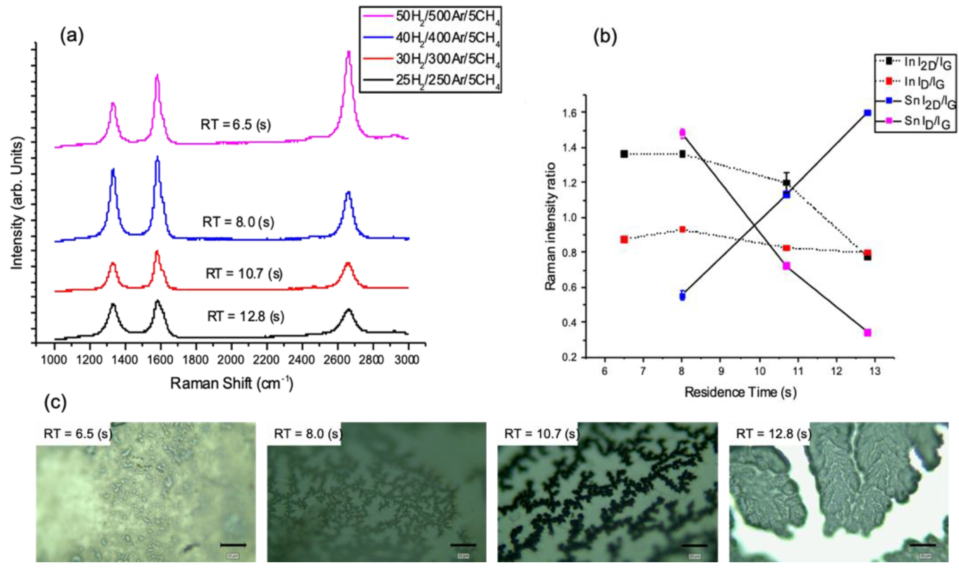
Initially, the gas flow rate of H2 and Ar was increased whilst keeping CH4 at a constant flow rate of 5 sccm. The residence time is inversely proportional to the total gaseous mass flow rate in a reactor, assuming laminar flow [20]. Thus, this series of experiments gave different residence times and CH4 concentrations in the reactor (Table S2). This was found to significantly affect the growth of graphene deposition on liquid In.
The results on liquid In, as shown in Figure 1, display different behaviour to that observed on Sn in our previous study. For most of the In experiments, multi-layer to graphite films with high defects densities were produced (Figure 1a,b). However, flow rate 50 H2/500 Ar/5 CH4 (sccm), which corresponds to a residence time of 6.5 s, shows an increase in the intensity of the 2D band with respect to the G band, indicating a bilayer graphene film. The film coverage was highly developed when using a shorter residence time (Figure 1c), as well as producing better graphene quality, the opposite to what was obtained in graphene on liquid Sn. This results suggests a better catalytic behaviour for the In over the Sn. In addition, increased CH4 concentration in the CVD reactor did not lead to the formation of amorphous carbon on the surface of liquid In, indicating a self-limiting nature that avoided any excess carbon depositing as adlayers. Thus, despite the residence time, the deposited film retained its crystalline structure. Furthermore, the decreased concentration of hydrocarbons led to thinner graphene flakes that could be explained by the deposition rate increasing with the excess presence of the active species near the substrate’s surface. Therefore, reducing the CH4 concentration by scaling up H2 and Ar flow rates resulted in the deposition of a reduced number of graphene layers. This is discussed further in Section 2.1.3.
2.1.2. The Effect of Hydrogen Flow Rate
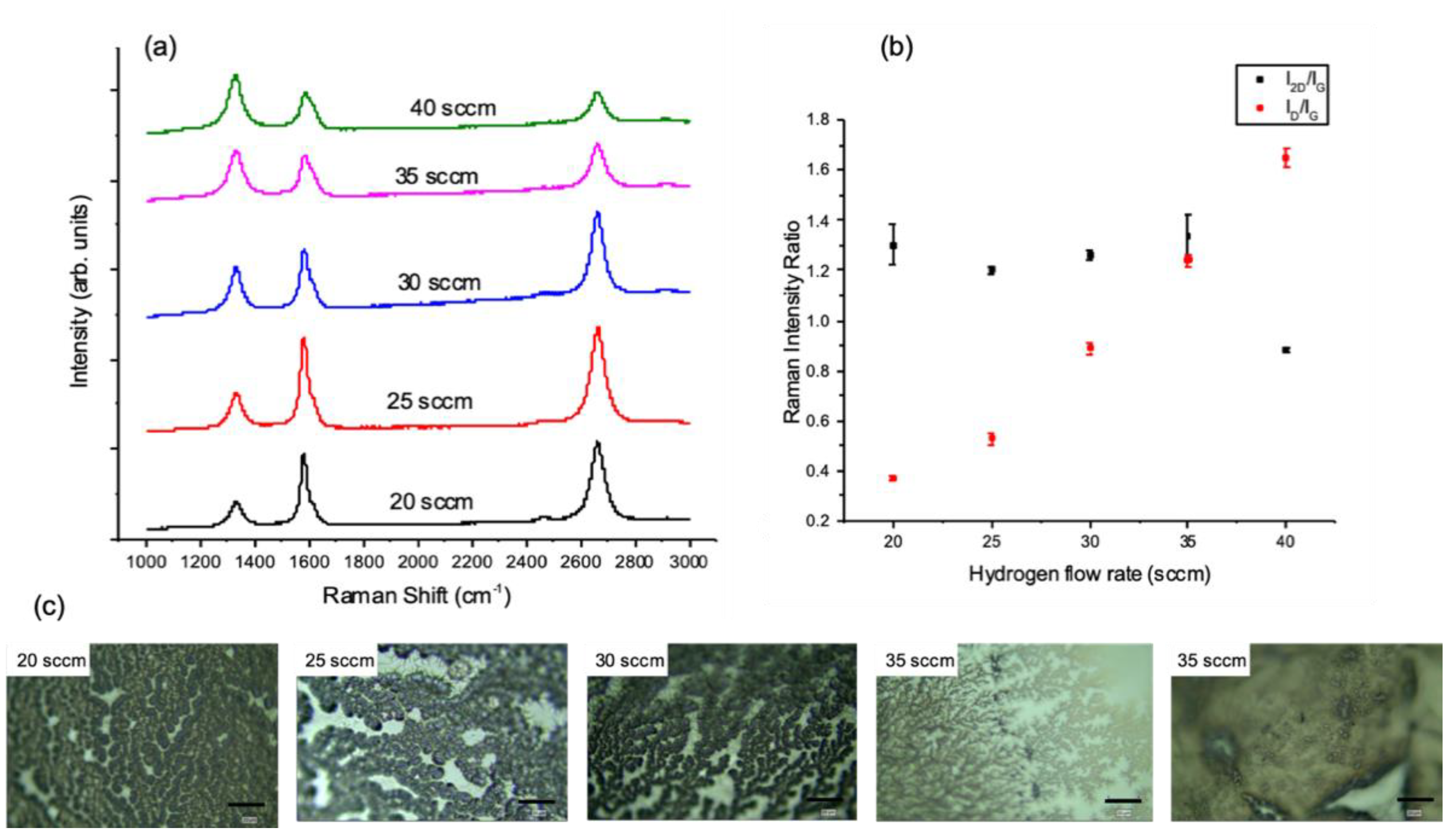
The catalytic nature of In is unknown due to the lack of literature, but the following sections can provide an insight into the crucial factors that affect APCVD graphene growth on liquid In. The effect of H2 flow rate on the deposition of APCVD graphene on liquid In was studied by varying the H2 flow rates in the range of 20–40 sccm, while other growth parameters were held constant (Table S3).
As shown in the optical images (Figure 2c) which illustrate the deposited graphene films on liquid In, the degree of coverage was found to vary. The graphene film reached full coverage at the lowest H2 flow rate of 20 sccm, giving PH = 38.6 mbar, in agreement with the H2 effect on the graphene deposition on liquid Sn [10]. Given the lack of data regarding H2 solubility in In, this observation of the H2 effect may lead to the conclusion that, similar to Sn, In has a low H2 solubility.
The Raman results from the graphene on the In (Figure 2a,b) show that the intensity ratio ID/IG decreases with decreasing H2 flow rates, implying that the graphene crystals’ size increases and the density of defects decreases as the H2 flow is reduced to the experimental limit of 20 sccm. These results can thus be described by the hypothesis that for substrates with low hydrogen solubility, the H2 molecules are governed by surface reaction as fewer molecules diffuse into the bulk of the substrate; thus, a high flow rate is not required. The H–H recombination is believed to be more likely at higher H2 flow rates, which leads to more available surface sites and hence causing non-uniform graphene nucleation and growth. Therefore, In does not require high H2 flow rates in order to provide sufficient surface sites for CH4 chemisorption for the subsequent deposition of graphene.
2.1.3. The Effect of Reactant Species (H2 and CH4) Partial Pressure
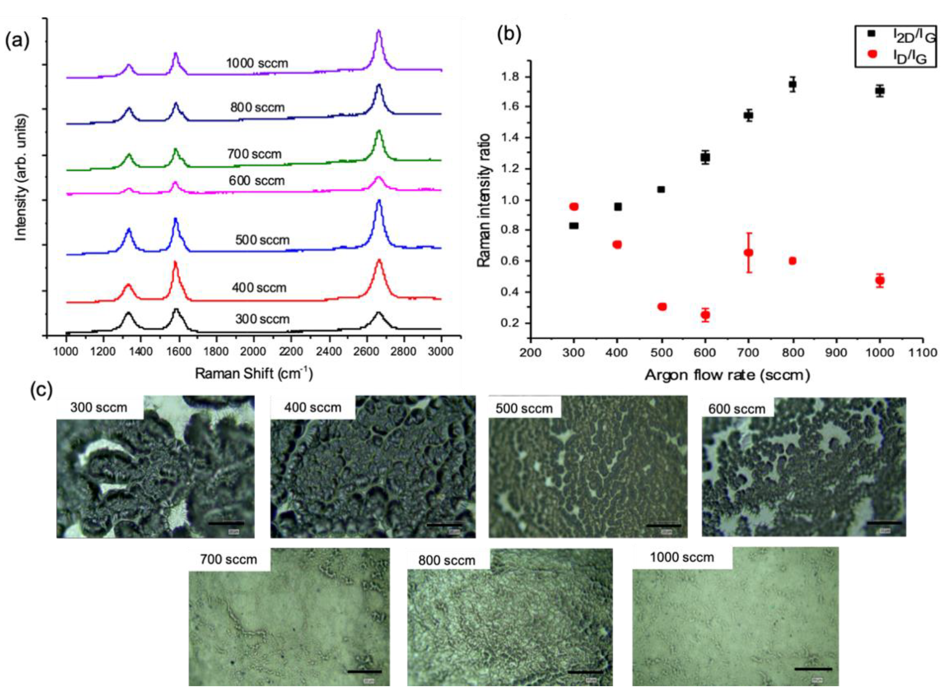
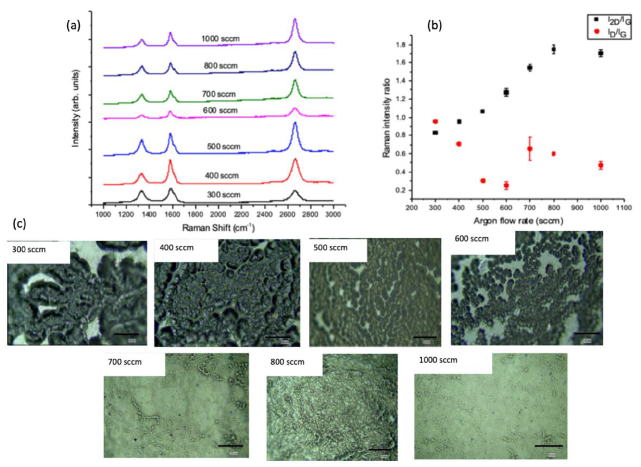
A range of Ar flow rates was used (300–1000 sccm) to lower the PH+CH in the range of 62.3–19.7 mbar (Table S4). This variation of the Ar flow rate also directly affected the total gas flow rate, which subsequently affected the residence time of the active species in the hot zone of the CVD reactor. In order to eliminate the effect of changing hydrogen to hydrocarbon ratio and instead solely investigate the effect of partial pressure of the active species in the reaction chamber (PH+CH), H2 and CH4 flow rates were held constant. The reactor was limited to a maximum possible Ar flow rate of 1000 sccm due to the MFC fitted. The number of layers, defects density, and surface coverage of the graphene films grown were assessed for each different Ar flow rate.
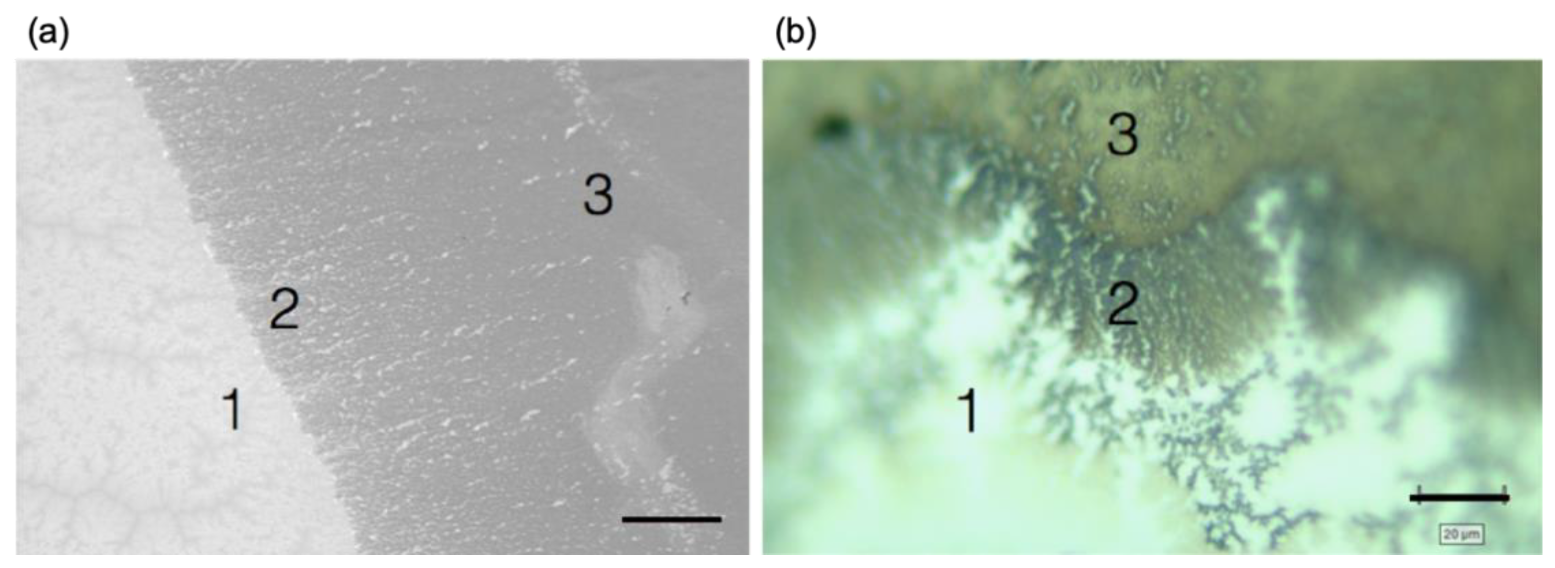
An immediate difference between the growth conditions, which was visible even by eye, was that the degree of coverage of the deposited film increased with increasing PH+CH (Figure 3c). Optical images identified that the films at the highest PH+CH = (77.9 and 59.6 mbar) were thick and comprised of sooty deposits. These thick films had a high ID/IG ≈ 1, as well as a right shoulder in the G peak, indicating phonon scattering from in-plane defects rather than stacking induced disorder. Whereas, the incomplete films which were grown at the lower concentrations comprised of mono- to few-layer graphene. Furthermore, the graphene films obtained at low PH+CH were found to deposit predominantly at the exhaust end of the reaction tube (Figure 4 and Figure S2).
This positional dependence implies that the film was produced on the limits of its growth conditions (hence its higher quality nature) and is believed to be related to the spatial concentration of methyl radicals (). These radicals were produced by the cracking of CH4 as the gas passed along the hot zone. Thus the parts of the sample’s surface near the inlet had no graphene deposition due to an insufficient amount of active species in their non-equilibrium state. Li et al. observed a similar behaviour using Cu foils, and also related it to the gas phase composition changes within the reaction chamber, with the gas nearing equilibrium as the residence time increased along the reaction zone [21].
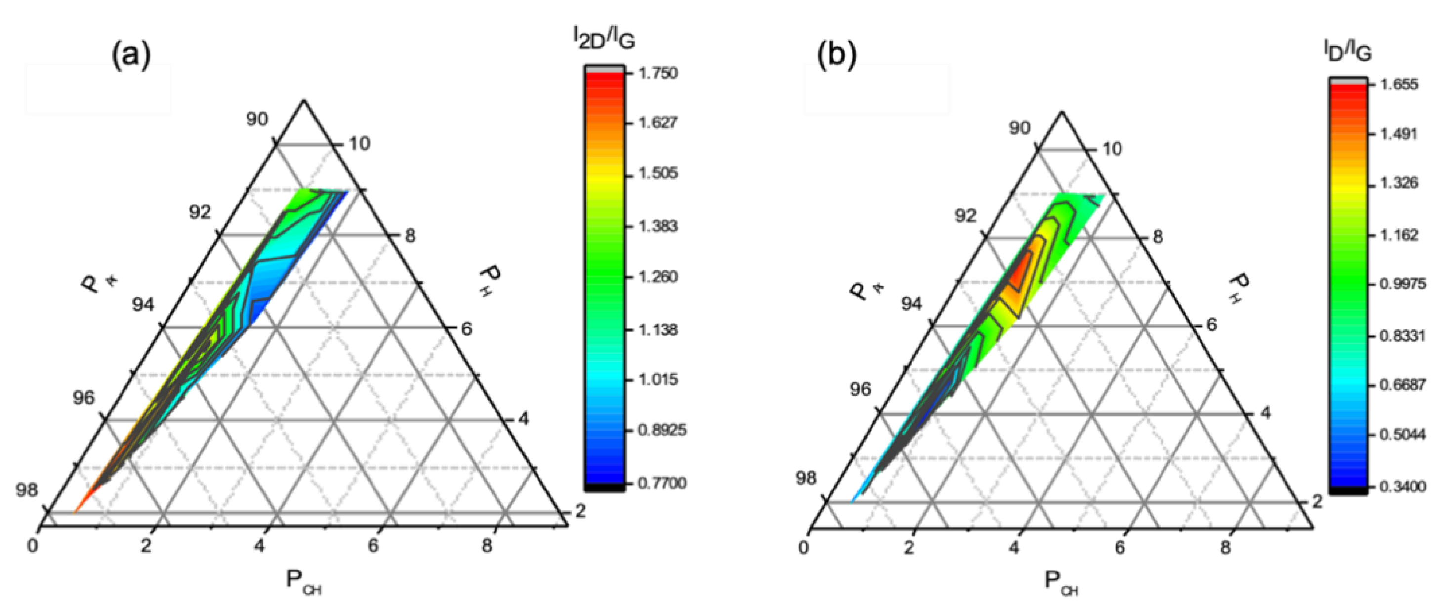
In the case of In, the ternary plot in Figure 5 shows that the best graphene quality, based on the highest I2D/IG and lowest ID/IG, are obtained at low hydrocarbon and hydrogen partial pressures (PH and PCH) as well as high argon partial pressure PAr. This agrees with the literature regarding graphene grown by an APCVD system on Cu, where the produced films tend to have a few-layer graphene nature with a high defect density at high partial pressures of the reactive gases. However, the graphene film quality was found to be enhanced when the hydrocarbon species were highly diluted [22,23,24]. The negligible carbon solubility of In [25] could be the main reason for similar behaviour to that of Cu. As a driving force, low PH+CH affects the carbon adsorbates’ concentration as it decreases on the surface of the substrate, which is possibly the reason behind the formation of a monolayer graphene film, while when it increases, graphene layers increase accordingly [26].
2.1.4. The Effect of Growth Time
As demonstrated, the quality of the grown graphene increases with reducing partial pressure of the hydrocarbon reactants. However, these conditions also lead to the poor coverage, leaving only a small area of the sample’s surface covered with graphene. Hence, a longer growth time of 15 min was used to grow graphene with Ar flow rate four times high.
The longer growth time was found to have no major effect on the degree of graphene coverage (Figure 6c) compared to that produced in a shorter time (Figure 3c). The optical images presented in (Figure 6c) were of the grown graphene film on the small area of the sample’s surface. Another observation is that the CVD reaction tube became less transparent due to the carbon deposition on its inner walls (Figure S2). This observation suggests that the effect of positional dependence persists at a given growth temperature despite the use of different growth times. This makes the conversion rate of CH4 to graphene solely dependent on PH+CH and the reactants’ residence time. Longer growth time only led to an increase in exposure time to the active carbon species in the gas downstream. This caused an undesired accumulation of carbon snowing on the inner walls of the reaction tube.
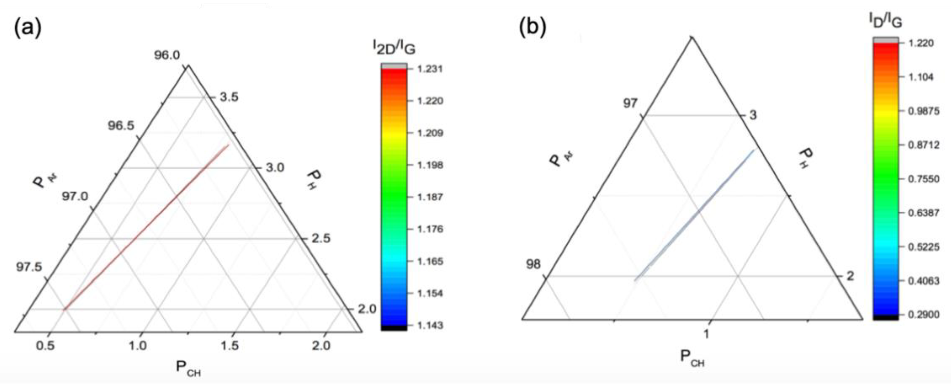
Interestingly, at longer growth time, the I2D/IG ratio was found to decrease to 1.2 for all the PH+CH used at higher Ar flow rates, in comparison to using shorter growth time where the Raman intensity ratio is in agreement with the reported value for bilayer graphene [27]. Thus, for growth conditions that are suitably carbon lean, the graphene growth self-limits to the bilayer. Increasing the growth time can also be seen to result in a line in the ternary plot which is a constant as the quality of graphene film remains insensitive to Ar flow rate at longer growth times (Figure 7).
2.2. CVD Graphene Growth on Liquid Cu-In Alloys-the Study of Catalytic Activity of Copper
The effect of introducing Cu at different dosages to In to form Cu-In alloy is explored in this section. Cu is the most favourable catalyst for CVD graphene growth and produces high quality graphene with a complete absence of D band, indicating a defect-free film. However, increasing the content of Cu in a Cu–Sn alloy was found previously to degrade graphene quality when optimum growth conditions for pure liquid Sn substrate were used [10].
Similarly, the Cu-In alloys of five different compositions were used to grow graphene using the optimum conditions established for pure liquid In substrates (Table S5). This study involved monitoring the changes in graphene quality, with respect to the number of layers and density of defects.
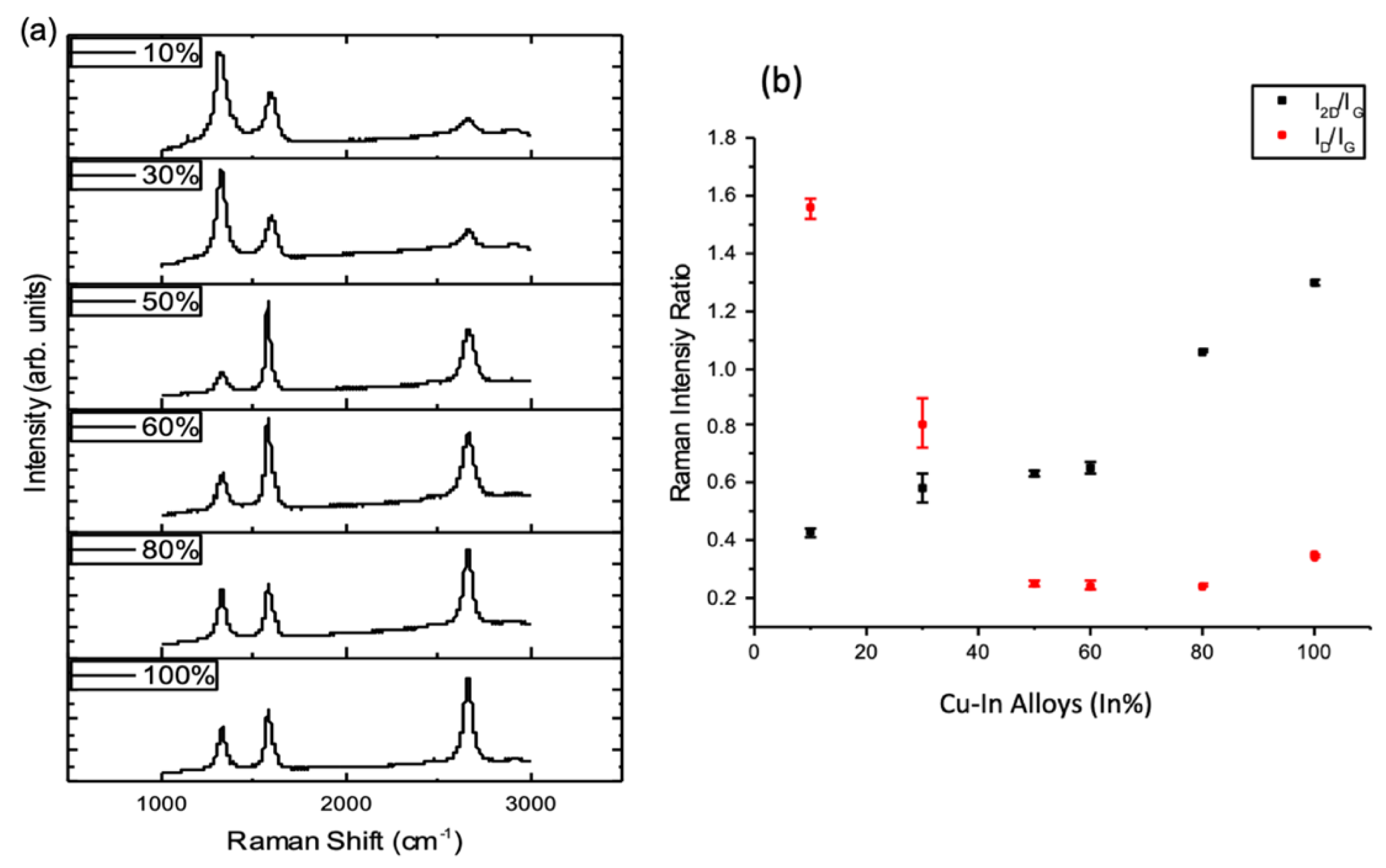
An increased number of layers of the grown graphene film can be observed from the decreased Raman ratio I2D/IG as the Cu wt.% increased in the Cu-In alloy (Figure 8). This result agrees with the previous results of the Cu-Sn system. As described earlier, the catalytic nature of Cu that aided the dehydrogenation of CH4 led to excess carbon species in the central hot zone of the furnace tube and above the growth substrate. Therefore, the presence of excess carbon, in addition to the change in carbon and hydrogen solubility and other surface and bulk properties based on the different alloy compositions, affected the material’s catalytic nature and, therefore, the deposition kinetics.
The graphene density of defects within the film drastically increased at Cu70%–In30% and Cu90%–In10% as the ratio ID/IG had an average value of 0.8 and 1.5, respectively, consistent with the deposition of amorphous carbon rather than crystalline graphene. ID/IG remains very close for the other compositions, with the major difference occurring in the number of graphene layers, as this changes from monolayer to bilayer, with few layer graphene and amorphous carbon arising due to the increased Cu wt.%.
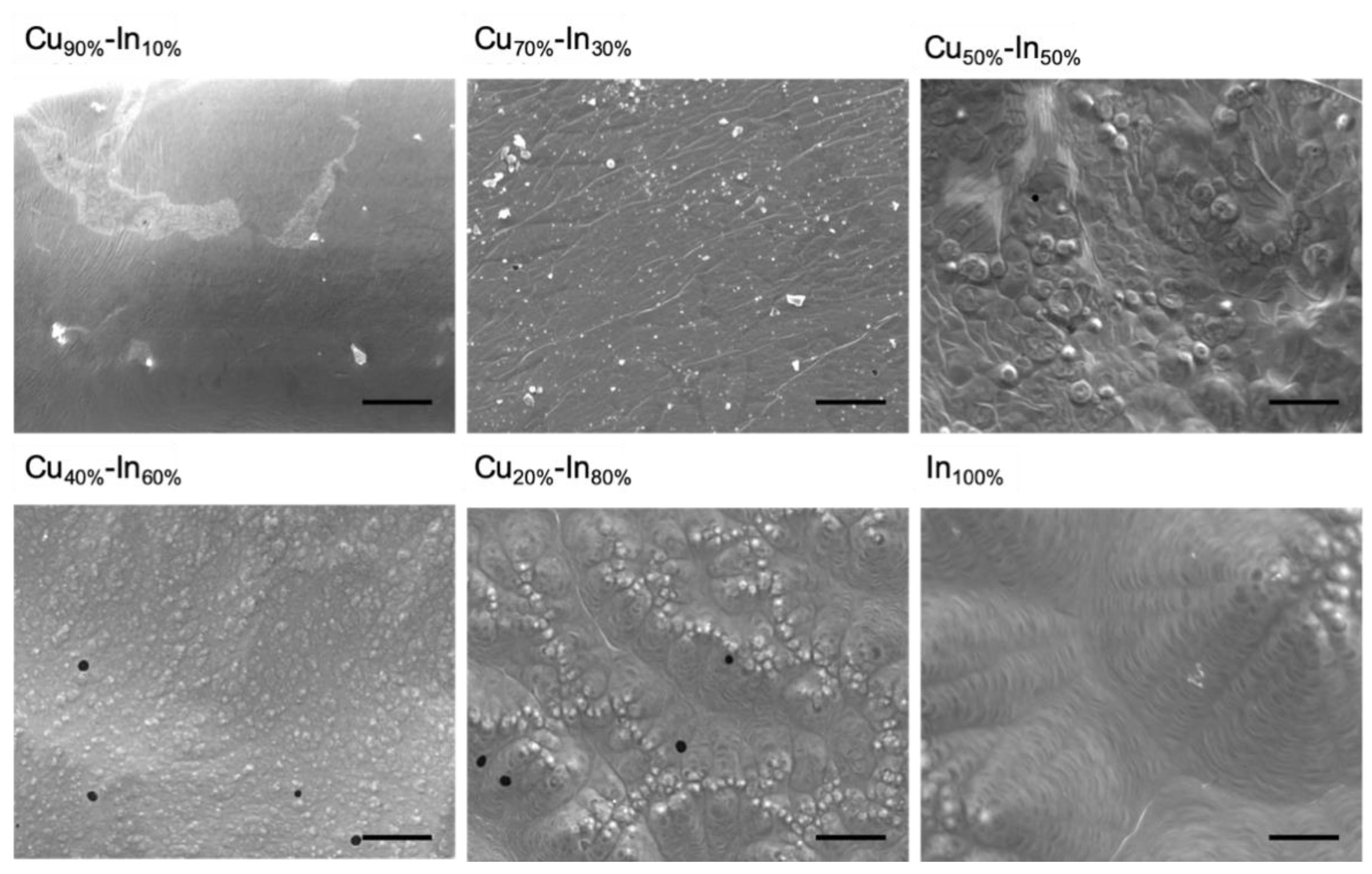
SEM images of 100 % and 80 % In reveal a bumpy surface, even though the graphene grown was still monolayer/bilayer in nature (Figure 9). This could be due to the contraction and shrinkage of the In-rich surface during solidification, causing folds in the graphene film. Liquid In has high surface tension that reduces its thermally induced roughness, when, for example, compared with alkali metals which have low surface tension [28]. The thermal expansion coefficient of In is reported to be 32.1 μm/(m∙K) at 25 °C and it should vary linearly with the change in temperature [29]. Therefore, the large difference between the melting point of In and the growth temperature, 963.4 °C, was expected to lead to an increased thermal contraction during the post-growth cooling process. At higher Cu wt.%, a smoother surface was obtained due to the lower thermal expansion of Cu, which is almost half that of In, with a value of 16.5 μm/(m∙K) at 25 °C.
3. Materials and Methods
Pure In (99.995%) (melting point 156 °C) and Cu (99.9999%) (melting point 1085 °C) metals were used (Goodfellow, Wrexham, UK) as growth substrates, held in tungsten boats (Agar Scientific, Elektron Technology, Cambridge, UK). Cu-In alloys were prepared using an arc-melting technique; elemental pure Cu and In were selected to give a total weight of 5 g at various nominal compositions (10, 30, 50, 60, and 80 of In wt.%) with their compositions given in Table S1.
In all CVD runs, the samples (substrate/W boat) were placed at the centre of the isothermic zone of the reaction tube. Air was then evacuated from the reaction tube using a rotary pump until it reached a pressure of ≈2.3 × 10⁻³ mbar, followed by back-filling the tube with hydrogen/argon mixture until it reached atmospheric pressure. The furnace was then switched on and the temperature was held at 1120 °C for 30 min. The growth step began when hydrocarbon feedstock was introduced to the reaction tube using methane gas for the duration of the required growth time at the same temperature of 1120 °C. Then, the methane flow and furnace were switched off at the same time and the tube was cooled down naturally under the flow of hydrogen/argon mixture, which was kept constant similar to the flow rate used during the entire CVD run for each experiment. Each CVD run was typically repeated 3–5 times to ensure consistency (a schematic diagram is illustrated in Figure S1).
Field emission gun scanning electron microscopy (FEG-SEM) (FEGSEM, FEI, Eindhoven, Netherlands) was used for the characterisation of the as-grown graphene. An accelerating voltage of 8 kV was used with a maximum working distance of 10 mm.
Raman spectroscopy was the main technique used to investigate the graphene grown on the different substrates. All Raman measurements were conducted using a Renishaw inVia system with an excitation laser wavelength of 633 nm (Renishaw, Wooton-under-Edge, UK). The main graphene characteristic peaks (D at 1350 cm−1, G at 1583 cm−1, and 2D at 2670 cm−1) were fitted using mixed Lorentzian–Gaussian functions in the Wire 4.2TM software (Renishaw, Wooton-under-Edge, UK)). The software was used to calculate the band intensity ratio, I2D/IG and ID/IG. Those band intensity ratios were used to reveal valuable information about the number of graphene layers by considering I2D/IG and the defects density by ID/IG [30,31,32,33]. Optical images were taken by the optical microscope Leica DM2700M (Leica Microsystems Ltd., Milton Keynes, UK) which is attached to the Renishaw Raman system.
4. Conclusions
APCVD graphene was sucessfully grown on a liquid In substrate, showing In as a low melting point metal substrate with possibly good catalytic properties. The graphene growth on In was insensitive to the CH4 concentration and at the highest obtained concentration, the graphene grown retained its crystalline nature with no formation of amorphous carbon. The shortest reactants’ residence time of 6.5 s led to a higher graphene quality compared to that gorwn under the longer residence times, again indicating the catalytic nature of In. The H2 flow rate was inversally related to the graphene crystals’ size increase and density of defects. The effect of the diluent gas, Ar, in terms of reducing the partial pressure of the hydrocarbon species while holding the H2 to CH4 ratio constant, showed better graphene quality as PH+CH decreased. However, the graphene film had many breakages in it at significantly low PH+CH. Longer growth times were examined at high Ar flow rates but these resulted in no enhancement in the film coverage, although a thicker film was obtained.
Cu-In alloy was used in five different compositions for APCVD graphene growth, utilising the optimised In growth recipe, to examine the effect of introducing Cu into the alloy system. As Cu is a strong catalyst, this catalytic nature aided faster CH4 cracking, resulting in a richer carbon environment. This was indicated by the number of layers in the graphene grown increasing with the increase of Cu-wt.% in the Cu-In alloy. This extended study of investigating the relationship between the physical properties (e.g., hydrogen and carbon solubility) of the substrate and determining the optimum conditions for the growth of CVD graphene shall provide great insight into the advances of CVD graphene synthesis. A better control over the quality of the produced graphene can be obtained by having such a matrix of correlation between substrate’s properties and growth parameters.
Supplementary Materials
The following are available online at https://0-www-mdpi-com.brum.beds.ac.uk/article/10.3390/catal11111318/s1, Figure S1: Schematic of the used CVD apparatus, Table S1: The weight of elemental metal used to form each Cu-In alloy composition, Table S2: Summary of the used APCVD graphene growth parameters on liquid In to study the effect of CH4 concentration and residence time, Table S3: APCVD graphene growth parameters on liquid In using different H2 flow rates, Table S4: APCVD graphene growth parameters on liquid In using different Ar flow rates, Figure S2: Photograph showing the position of the sample in the APCVD reactor in the middle of the furnace hot zone while the sooty patch where graphene was deposited on the surface is shown as observed, towards the exhaust end of the reactor, Figure S3: APCVD graphene grown on liquid In using Ar flow rate of 1000 sccm and a growth time of 15 min. (a) Optical image of the graphene film showing three regions noted by numbers where one has no graphene, two has early deposition and three is the grown graphene film. (b) Photograph of the CVD reaction tube that shows the change in its colour as it becomes less transparent. This shows that the growth time does not affect the degree of coverage but leads to a slight increase in the sooting of the reaction tube. Table S5: Optimised growth parameters for APCVD graphene on liquid In.
Author Contributions
I.A.K. and B.D. supervised the work conducted in this research paper including discussions and results interpretations. M.A.S. designed and conducted the experimental work (synthesis, characterisation and analysis) of this research paper and wrote the manuscript. All authors have read and agreed to the published version of the manuscript.
Funding
The authors acknowledge Kuwait Institute for Scientific Research for funding this project and I.A.K. acknowledges the Royal Academy of Engineering and Morgan Advanced Materials for funding his Chair.
Conflicts of Interest
The authors declare no conflict of interest.
References
- Quintana, M.; Tapia, J.I.; Prato, M. Liquid-phase exfoliated graphene: Functionalization, characterization, and applications. Beilstein J. Nanotechnol. 2014, 5, 2328–2338. [Google Scholar] [CrossRef] [PubMed] [Green Version]
- Ciesielski, A.; Samori, P. Graphene via sonication assisted liquid-phase exfoliation. Chem. Soc. Rev. 2014, 43, 381–398. [Google Scholar] [CrossRef] [PubMed]
- Haar, S.; Bruna, M.; Lian, J.X.; Tomarchio, F.; Olivier, Y.; Mazzaro, R.; Morandi, V.; Moran, J.; Ferrari, A.C.; Beljonne, D.; et al. Liquid-Phase Exfoliation of Graphite into Single- and Few-Layer Graphene with alpha-Functionalized Alkanes. J. Phys. Chem. Lett. 2016, 7, 2714–2721. [Google Scholar] [CrossRef] [PubMed] [Green Version]
- Novoselov, K.S.; Geim, A.K.; Morozov, S.V.; Jiang, D.; Zhang, Y.; Dubonos, S.V.; Grigorieva, I.V.; Firsov, A.A. Electric field effect in atomically thin carbon films. Science 2004, 306, 666–669. [Google Scholar] [CrossRef] [PubMed] [Green Version]
- Huet, B.; Raskin, J.-P. Pressure-Controlled Chemical Vapor Deposition of Single-Layer Graphene with Millimeter-Size Domains on Thin Copper Film. Chem. Mater. 2017, 29, 3431–3440. [Google Scholar] [CrossRef]
- Congqin Miao, C.Z.; Owen, L.; Ya-Hong, X. Chemical Vapor Deposition of Graphene, Physics and Applications of Graphene-Theory; InTech: Rijeka, Croatia, 2011. [Google Scholar]
- Li, X.; Colombo, L.; Ruoff Rodney, S. Synthesis of Graphene Films on Copper Foils by Chemical Vapor Deposition. Adv. Mater. 2016, 28, 6247–6252. [Google Scholar] [CrossRef] [PubMed]
- Ani, M.H.; Kamarudin, M.A.; Ramlan, A.H.; Ismail, E.; Sirat, M.S.; Mohamed, M.A.; Azam, M.A. A critical review on the contributions of chemical and physical factors toward the nucleation and growth of large-area graphene. J. Mater. Sci. 2018, 53, 7095–7111. [Google Scholar] [CrossRef] [Green Version]
- Losurdo, M.; Giangregorio, M.M.; Capezzuto, P.; Bruno, G. Graphene CVD growth on copper and nickel: Role of hydrogen in kinetics and structure. Phys. Chem. Chem. Phys. 2011, 13, 20836–20843. [Google Scholar] [CrossRef]
- Saeed, M.A.; Kinloch, I.A.; Derby, B. Atmospheric Pressure Catalytic Vapor Deposition of Graphene on Liquid Sn and Cu-Sn Alloy Substrates. Nanomaterials 2020, 10, 2150. [Google Scholar] [CrossRef]
- Yu, Q.; Jauregui, L.A.; Wu, W.; Colby, R.; Tian, J.; Su, Z.; Cao, H.; Liu, Z.; Pandey, D.; Wei, D.; et al. Control and characterization of individual grains and grain boundaries in graphene grown by chemical vapour deposition. Nat. Mater. 2011, 10, 443–449. Available online: http://0-www-nature-com.brum.beds.ac.uk/nmat/journal/v10/n6/abs/nmat3010.html#supplementary-information (accessed on 20 August 2021). [CrossRef] [PubMed] [Green Version]
- Geng, D.; Wu, B.; Guo, Y.; Huang, L.; Xue, Y.; Chen, J.; Yu, G.; Jiang, L.; Hu, W.; Liu, Y. Uniform hexagonal graphene flakes and films grown on liquid copper surface. Proc. Natl. Acad. Sci. USA 2012, 109, 7992–7996. [Google Scholar] [CrossRef] [Green Version]
- Saeed, M.; Robson, J.D.; Kinloch, I.A.; Derby, B.; Liao, C.-D.; Al-Awadhi, S.; Al-Nasrallah, E. The formation mechanism of hexagonal Mo2C defects in CVD graphene grown on liquid copper. Phys. Chem. Chem. Phys. 2020, 22, 2176–2180. [Google Scholar] [CrossRef]
- Fan, Y.; He, K.; Tan, H.; Speller, S.; Warner, J.H. Crack-Free Growth and Transfer of Continuous Monolayer Graphene Grown on Melted Copper. Chem. Mater. 2014, 26, 4984–4991. [Google Scholar] [CrossRef]
- Wu, Y.A.; Fan, Y.; Speller, S.; Creeth, G.L.; Sadowski, J.T.; He, K.; Robertson, A.W.; Allen, C.S.; Warner, J.H. Large Single Crystals of Graphene on Melted Copper Using Chemical Vapor Deposition. ACS Nano 2012, 6, 5010–5017. [Google Scholar] [CrossRef]
- Cho, S.-Y.; Kim, M.-S.; Kim, M.; Kim, K.-J.; Kim, H.-M.; Lee, D.-J.; Lee, S.-H.; Kim, K.-B. Self-assembly and continuous growth of hexagonal graphene flakes on liquid Cu. Nanoscale 2015, 7, 12820–12827. [Google Scholar] [CrossRef] [Green Version]
- Wu, B.; Geng, D.; Xu, Z.; Guo, Y.; Huang, L.; Xue, Y.; Chen, J.; Yu, G.; Liu, Y. Self-organized graphene crystal patterns. NPG Asia Mater. 2013, 5, e36. Available online: http://0-www-nature-com.brum.beds.ac.uk/am/journal/v5/n2/suppinfo/am201268s1.html (accessed on 15 August 2021). [CrossRef] [Green Version]
- Zeng, M.; Tan, L.; Wang, J.; Chen, L.; Rümmeli, M.H.; Fu, L. Liquid Metal: An Innovative Solution to Uniform Graphene Films. Chem. Mater. 2014, 26, 3637–3643. [Google Scholar] [CrossRef]
- Wang, J.; Zeng, M.; Tan, L.; Dai, B.; Deng, Y.; Rummeli, M.; Xu, H.; Li, Z.; Wang, S.; Peng, L.; et al. High-mobility graphene on liquid p-block elements by ultra-low-loss CVD growth. Sci Rep. 2013, 3, 2670. [Google Scholar] [CrossRef]
- Josiek, A.; Langlais, F. Residence-time dependent kinetics of CVD growth of SiC in the MTSH2 system. J. Cryst. Growth 1996, 160, 253–260. [Google Scholar] [CrossRef]
- Li, Z.; Zhang, W.; Fan, X.; Wu, P.; Zeng, C.; Li, Z.; Zhai, X.; Yang, J.; Hou, J. Graphene Thickness Control via Gas-Phase Dynamics in Chemical Vapor Deposition. J. Phys. Chem. C 2012, 116, 10557–10562. [Google Scholar] [CrossRef]
- Yao, Y.; Li, Z.; Lin, Z.; Moon, K.-S.; Agar, J.; Wong, C. Controlled Growth of Multilayer, Few-Layer, and Single-Layer Graphene on Metal Substrates. J. Phys. Chem. C 2011, 115, 5232–5238. [Google Scholar] [CrossRef]
- Lenski, D.R.; Fuhrer, M.S. Raman and optical characterization of multilayer turbostratic graphene grown via chemical vapor deposition. J. Appl. Phys. 2011, 110, 013720. [Google Scholar] [CrossRef] [Green Version]
- Luo, Z.; Lu, Y.; Singer, D.W.; Berck, M.E.; Somers, L.A.; Goldsmith, B.R.; Johnson, A.T.C. Effect of Substrate Roughness and Feedstock Concentration on Growth of Wafer-Scale Graphene at Atmospheric Pressure. Chem. Mater. 2011, 23, 1441–1447. [Google Scholar] [CrossRef]
- Rao, R.; Eyink, K.G.; Maruyama, B. Single-walled carbon nanotube growth from liquid gallium and indium. Carbon 2010, 48, 3971–3973. [Google Scholar] [CrossRef]
- Wu, B.; Geng, D.; Guo, Y.; Huang, L.; Xue, Y.; Zheng, J.; Chen, J.; Yu, G.; Liu, Y.; Jiang, L.; et al. Equiangular Hexagon-Shape-Controlled Synthesis of Graphene on Copper Surface. Adv. Mater. 2011, 23, 3522–3525. [Google Scholar] [CrossRef] [PubMed]
- Dusari, S.; Goyal, N.; Debiasio, M.; Kenda, A. Raman spectroscopy of graphene on AlGaN/GaN heterostructures. Thin Solid Film. 2015, 597, 140–143. [Google Scholar] [CrossRef]
- Tostmann, H.; DiMasi, E.; Pershan, P.S.; Ocko, B.M.; Shpyrko, O.G.; Deutsch, M. Surface structure of liquid metals and the effect of capillary waves: X-ray studies on liquid indium. Phys. Rev. B 1999, 59, 783–791. [Google Scholar] [CrossRef] [Green Version]
- Hidnert, P.B.; Blair, M.G. Thermal expansivity and density of indium. J. Res. Natl. Bur. Stand. 1943, 30, 427. [Google Scholar] [CrossRef]
- Ferrari, A.C.; Meyer, J.C.; Scardaci, V.; Casiraghi, C.; Lazzeri, M.; Mauri, F.; Piscanec, S.; Jiang, D.; Novoselov, K.S.; Roth, S.; et al. Raman Spectrum of Graphene and Graphene Layers. Phys. Rev. Lett. 2006, 97, 187401. [Google Scholar] [CrossRef] [PubMed] [Green Version]
- Cançado, L.G.; Takai, K.; Enoki, T.; Endo, M.; Kim, Y.A.; Mizusaki, H.; Jorio, A.; Coelho, L.N.; Magalhães-Paniago, R.; Pimenta, M.A. General equation for the determination of the crystallite size La of nanographite by Raman spectroscopy. Appl. Phys. Lett. 2006, 88, 163106. [Google Scholar] [CrossRef]
- Lucchese, M.M.; Stavale, F.; Ferreira, E.H.M.; Vilani, C.; Moutinho, M.V.O.; Capaz, R.B.; Achete, C.A.; Jorio, A. Quantifying ion-induced defects and Raman relaxation length in graphene. Carbon 2010, 48, 1592–1597. [Google Scholar] [CrossRef]
- Saeed, M.; Alshammari, Y.; Majeed, S.A.; Al-Nasrallah, E. Chemical Vapour Deposition of Graphene—Synthesis, Characterisation, and Applications: A Review. Molecules 2020, 25, 3856. [Google Scholar] [CrossRef] [PubMed]
Figure 1.
(a) Raman spectra of the APCVD graphene on liquid In using different reactants residence times, (b) Average Raman intensity ratios of I2D/IG and ID/IG of the grown graphene on liquid In (dotted dash lines) and on liquid Sn from previous study [10] (doted solid lines) with respect to residence time (error bars are smaller than some of the data points). (c) Optical images of the as-grown graphene films (the dark areas) (scale bar: 20 µm), some blurriness is due to the surface curvature of the solidified In (APCVD, T = 1120 C, (25–50) H2/(250–500) Ar/5 CH4 sccm, t = 5 min).

Figure 2.
(a) Raman spectra of the graphene grown on liquid In, showing the effect of changing the H2 flow rate. (b) Average Raman intensity ratio of the I2D/IG and ID/IG values vs. the H2 flow rate based on map data (error bars are smaller than some of the data points). (c) Optical images of the as- grown graphene films (scale bar: 20 µm), some blurriness is due to the surface curvature of the solidified In (APCVD, T = 1120 °C, (20–40) H2/500 Ar/5 CH4 sccm, t = 5 min).

Figure 3.
(a) Raman spectra of the graphene grown on liquid In showing the effect of changing the Ar flow rate. (b) Average Raman intensity ratio for the I2D/IG and ID/IG values vs. the Ar flow rate based on map data (error bars are smaller than some of the data points). (c) Optical images of the grown graphene films (scale bar: 20 µm), some blurriness is due to the surface curvature of the solidified In (APCVD, T = 1120 °C, 20 H2/(300–1000) Ar/5 CH4 sccm, t = 5 min).

Figure 4.
(a) and (b) represent SEM and optical images, respectively, of APCVD graphene on liquid In, using Ar flow rate of 1000 sccm. Both images show three regions where the graphene growth develops, (1) shows no deposition (2) the area of early deposition as a transition stage as dendritric graphene merges to initiate a more continuous graphene film in (3). The flow direction is in the direction of 1 to 3. (The SEM image was taken at low magnification in order to show the three regions with a scale bar of 100 μm, while the optical image scale bar is 20 μm).

Figure 5.
Ternary plots showing Raman intensity ratios as a function of gas partial pressures (PH2, PAr and PCH4), (a) I2D/IG and (b) ID/IG (All axes are normalised with respect to total gas pressure).
Figure 5.
Ternary plots showing Raman intensity ratios as a function of gas partial pressures (PH2, PAr and PCH4), (a) I2D/IG and (b) ID/IG (All axes are normalised with respect to total gas pressure).

Figure 6.
Summary of data of APCVD graphene on liquid In at high Ar flow rates (sccm), grown for 15 min (a) Raman spectra of APCVD graphene using high Ar flow rates (sccm) (b) optical images of the grown graphene film (scale bar 20 μm) and (c) Average Raman intensity ratio I2D/IG and ID/IG values vs. the Ar flow rate based on maps data (error bars are smaller than some data points). (Raman laser energy: 633 nm).

Figure 7.
Ternary plots showing Raman intensity ratios as a function of gas partial pressures (PH2, PAr and PCH4), (a) I2D/IG and (b) ID/IG using growth time of 15 min (all axes are normalised with respect to total gas pressure).
Figure 7.
Ternary plots showing Raman intensity ratios as a function of gas partial pressures (PH2, PAr and PCH4), (a) I2D/IG and (b) ID/IG using growth time of 15 min (all axes are normalised with respect to total gas pressure).

Figure 8.
(a) Raman spectra from points taken randomly on the surface of the deposited film for the different Cu-In compositions (In%). (b) A plot of the average Raman intensity ratios based on >100 points Raman maps, I2D/IG and ID/IG vs. the wt.% content of In in each Cu-In composition (error bars are smaller than some of the data points) (APCVD, T = 1120 °C, 20 H2/500 Ar/5 CH4 sccm, t = 5 min).

Figure 9.
SEM images of Cu-In alloys at different compositions after AP-CVD graphene growth, (Scale bar: 5 µm).
Figure 9.
SEM images of Cu-In alloys at different compositions after AP-CVD graphene growth, (Scale bar: 5 µm).

Publisher’s Note: MDPI stays neutral with regard to jurisdictional claims in published maps and institutional affiliations. |
© 2021 by the authors. Licensee MDPI, Basel, Switzerland. This article is an open access article distributed under the terms and conditions of the Creative Commons Attribution (CC BY) license (https://creativecommons.org/licenses/by/4.0/).
Share and Cite
MDPI and ACS Style
Saeed, M.A.; Kinloch, I.A.; Derby, B. Atmospheric Pressure Catalytic Vapor Deposition of Graphene on Liquid In and Cu-In Alloy Substrates. Catalysts 2021, 11, 1318. https://0-doi-org.brum.beds.ac.uk/10.3390/catal11111318
AMA Style
Saeed MA, Kinloch IA, Derby B. Atmospheric Pressure Catalytic Vapor Deposition of Graphene on Liquid In and Cu-In Alloy Substrates. Catalysts. 2021; 11(11):1318. https://0-doi-org.brum.beds.ac.uk/10.3390/catal11111318
Chicago/Turabian StyleSaeed, Maryam A., Ian A. Kinloch, and Brian Derby. 2021. "Atmospheric Pressure Catalytic Vapor Deposition of Graphene on Liquid In and Cu-In Alloy Substrates" Catalysts 11, no. 11: 1318. https://0-doi-org.brum.beds.ac.uk/10.3390/catal11111318
Note that from the first issue of 2016, this journal uses article numbers instead of page numbers. See further details here.