Structural, Optical, Band Edge and Enhanced Photoelectrochemical Water Splitting Properties of Tin-Doped WO3

Department of Materials Science and Engineering, Ajou University, Suwon 443-739, Korea
Catalysts 2019, 9(5), 456; https://0-doi-org.brum.beds.ac.uk/10.3390/catal9050456
Submission received: 11 May 2019
/
Revised: 16 May 2019
/
Accepted: 16 May 2019
/
Published: 17 May 2019
(This article belongs to the Special Issue Catalysts for Solar Fuels)
Abstract
:The substitutional doping of tungsten oxide (WO3) with metal ions demonstrates a promising approach to enhance its photoelectrochemical (PEC) water splitting efficiency. In this article, the substitutional doping of Sn ions into WO3 lattice and its effect on optical, electrical, band edge, and PEC water splitting properties are explored. Sn-doped WO3 thin films were synthesized using a facile hydrothermal method. The characterization data reveal that the doping of Sn alters the morphology, induces multiple crystal phases, effects the crystal orientation, reduces the band gap, and increases the carrier density of WO3. With the uniform distribution of Sn ions in WO3 and the decreased charge transfer resistance at the electrode/electrolyte interface, the doped WO3 show notable enhancement in its PEC activity compared to the undoped WO3. The band edge study revealed that the introduction of Sn in WO3 lattice causes an increase in the energy distance between the valence band edge and Fermi level and, at the same time, induces a downward shift in both the valence and conduction band edges towards higher potentials with respect to reversible hydrogen electrode (RHE). Conclusively, this work shows significant and new insights about Sn-doped WO3 photoanodes and their influence on PEC water splitting efficiency.

1. Introduction
A promising resolution to the global energy requirement of the future, along with the protection of environment, comes from the next generation and sustainable energy source hydrogen and its clean and carbon-free production via photoelectrochemical water splitting [1]. In photoelectrochemical (PEC) water splitting, a semiconductor is used to split water into H2 and O2 using abundant and sustainable resources, like sunlight and water [2,3]. The first successful demonstration of solar water splitting using TiO2 semiconductor was reported by Fujishima and Honda [4], and has initiated significant research attention and contributions that have continued until now. As a result, a variety of semiconductors were explored, researched, and reported as an active material for solar water splitting reaction. Notably, the well-matched optical, electrical properties, and stability of the metal oxides have demonstrated their active participation as useful electrode materials in PEC water splitting systems.
Among the various metal oxide materials utilized in PEC water splitting, tungsten oxide (WO3) has emerged as a promising candidate, due to its suitable physical and chemical properties [5,6]. The effective utilization of WO3 in solar water splitting was first demonstrated in 1976 by Hodes et al. [7]. Since then, significant research contributions have been reported. It was found that WO3 can absorb a maximum of ~12% of the incident solar light with a band gap of 2.6–2.8 eV. Ideally, based on its light absorption capability, as high as ~4.8% of solar energy to the hydrogen conversion efficiency could be extracted [8]. However, WO3 faces numerous limitations that affect its charge generation, separation, and transportation properties, that decrease its ability to carry out water splitting. Therefore, the structural, optical, and electrochemical properties of WO3 need to be tuned to increase its water splitting efficiency.
The tuning of the structural, optical, and electrochemical properties of WO3 could be achieved by various modifications that improve its PEC water splitting efficiency. In particular, the crystal structure, band gap, carrier density, and charge transport at the electrolyte interface are the most significant factors influencing water splitting efficiency. Among the existing crystal structures, monoclinic WO3 is known to be the most suitable crystal phase for PEC water splitting [9,10,11]. Therefore, it is essential to explore the possible modification through which the structural, optical, and electrical properties of monoclinic WO3 could be tuned and optimized without disrupting the crystal nature and stability. Hence, an effectively tuned monoclinic WO3 is expected to be beneficial for the water splitting reaction, compared to undoped WO3.
A recent study indicates that the substitutional doping of metal ions is an effective strategy of tuning the physical and chemical properties of WO3 [12,13,14,15]. Importantly, the type and extent of modification induced in doped WO3 mainly depend on the nature of dopant metal ion and its concentration [13,16,17]. Therefore, exploring a suitable dopant material for WO3 is essential for obtaining high efficiency in PEC water splitting [3]. Until now, various dopants, including Ti [16], Co [18], Mo [17], Zn [19], Bi [13], Ni [18], Nb [20], Cu [18], Al [21], Ta [22], Fe [23,24,25], Te [26], and Ba [27], have been employed to alter the structural, optical, electrical, and band edge properties of WO3 and to enhance its photocatalytic properties. Previously, Sn has been actively used as an effective dopant material for metal oxides, such as Fe2O3, to enhance its PEC water splitting properties [28,29], revealing its positive impact as a dopant material. Moreover, a detailed literature survey revealed that despite a few reports, no in-depth study has been reported regarding the synthesis and PEC properties Sn-doped WO3 thin films. Hence, it is essential to explore the effect of Sn doping on the structural, optical, electrical, band edge, and PEC water splitting properties of WO3.
Given this, we here synthesize and explore the effect of Sn doping on the PEC water splitting efficiency of WO3 thin films. To obtain the Sn-doped WO3 thin films, a facile single-step hydrothermal approach is utilized, that is proceeded by introducing the Sn precursor into a peroxopolytungstic acid (PTA) solution, followed by reaction at 150 °C. The Sn-doped WO3 thin films were characterized in detail to understand the effect on structural, crystallographic, optical, and electrical properties of WO3. Furthermore, Sn ions were found to be uniformly distributed in the WO3 crystals on the (fluorine doped tin oxide) FTO substrate, without affecting their adhesion. Using data from the absorbance, X-ray photoelectron spectroscopy, and Mott–Schottky (MS) analysis, an appropriate band edge positions of WO3 was plotted with respect to RHE potentials before and after doping with Sn ions. The electrochemical measurements revealed that Sn-doped WO3 thin films show increased photocurrent (at 1.23 V vs. RHE), incident photon-to-current efficiency (IPCE) and decreased charge transfer resistance across the electrode/electrolyte interface. The notable enhancement in the PEC properties of WO3 upon Sn doping was ascribed to the proper crystal facet orientation, decreased band gap, and significant increase of carrier density.
2. Results and Discussion
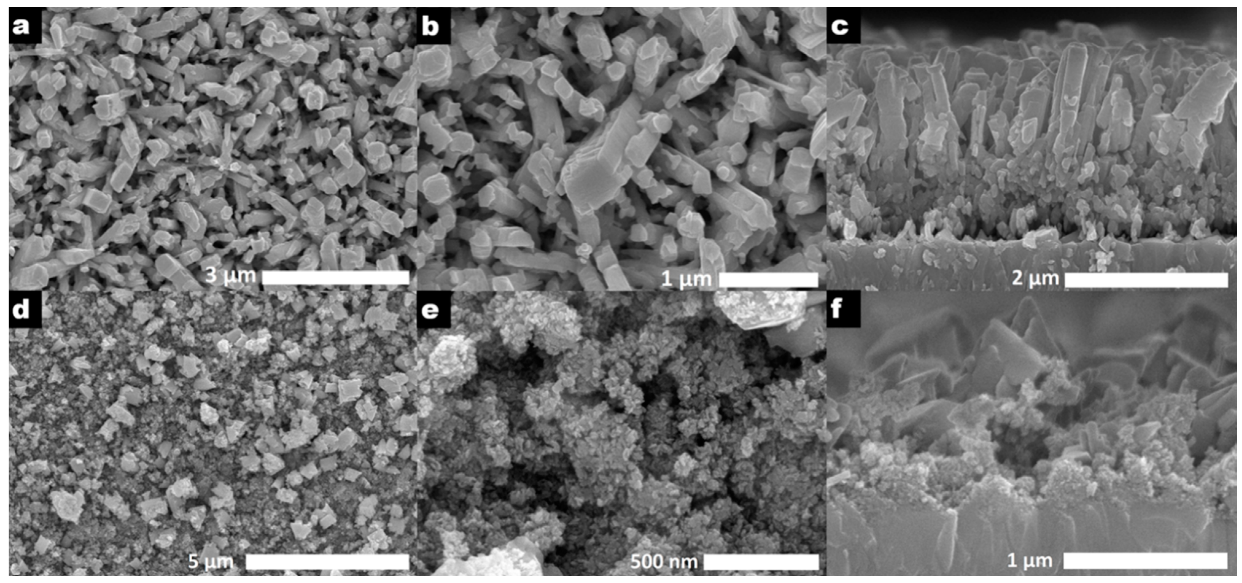
The hydrothermal synthesis method utilized in the present study allows for the precise tuning of Sn atom % in the WO3 lattice by controlling the Sn precursor concentration in the hydrothermal synthesis solution. Table S1 shows the amount of precursor solution taken in the synthesis solution and the atom % and wt % of Sn detected via EDS. Based on the PEC studies, the WO3 thin films doped with 0.8 atom % of Sn showed enhanced photocurrent compared to the samples doped with the other concentrations of Sn, and hence, were chosen for detailed characterization. Figure 1 shows the high- and low-resolution SEM images of undoped and Sn-doped WO3 thin films. The morphology of undoped WO3 (Figure 1a,b) appeared to be a mixture of nanoparticles, and nanorod structure assembled on the FTO substrate. After Sn doping, a significant change in morphology was observed, indicating the disappearance of nanorod morphology and the formation of smaller (5–10 nm) coagulated nanoparticles (Figure 1d,e) and the presence of larger (500–1000 nm) nanoparticles and plates at different places. This suggests that the substitution of Sn in crystal lattice affects the structure of WO3. The cross-section SEM image of undoped WO3 (Figure 1c) clearly shows the nanorod morphology assembled on the thin film of the nanoparticle layer. The thickness of the thin film was measured to be ~2 µm. Figure 1f shows the cross-section SEM image of Sn-doped WO3 thin film, confirming the change in morphology and the decrease in film thickness to 1 µm. Furthermore, the low-resolution SEM image confirmed the uniform deposition of doped WO3 throughout the FTO substrate with a reduced thickness, indicating that the doping of Sn affects the deposition amount of WO3 on the substrate.
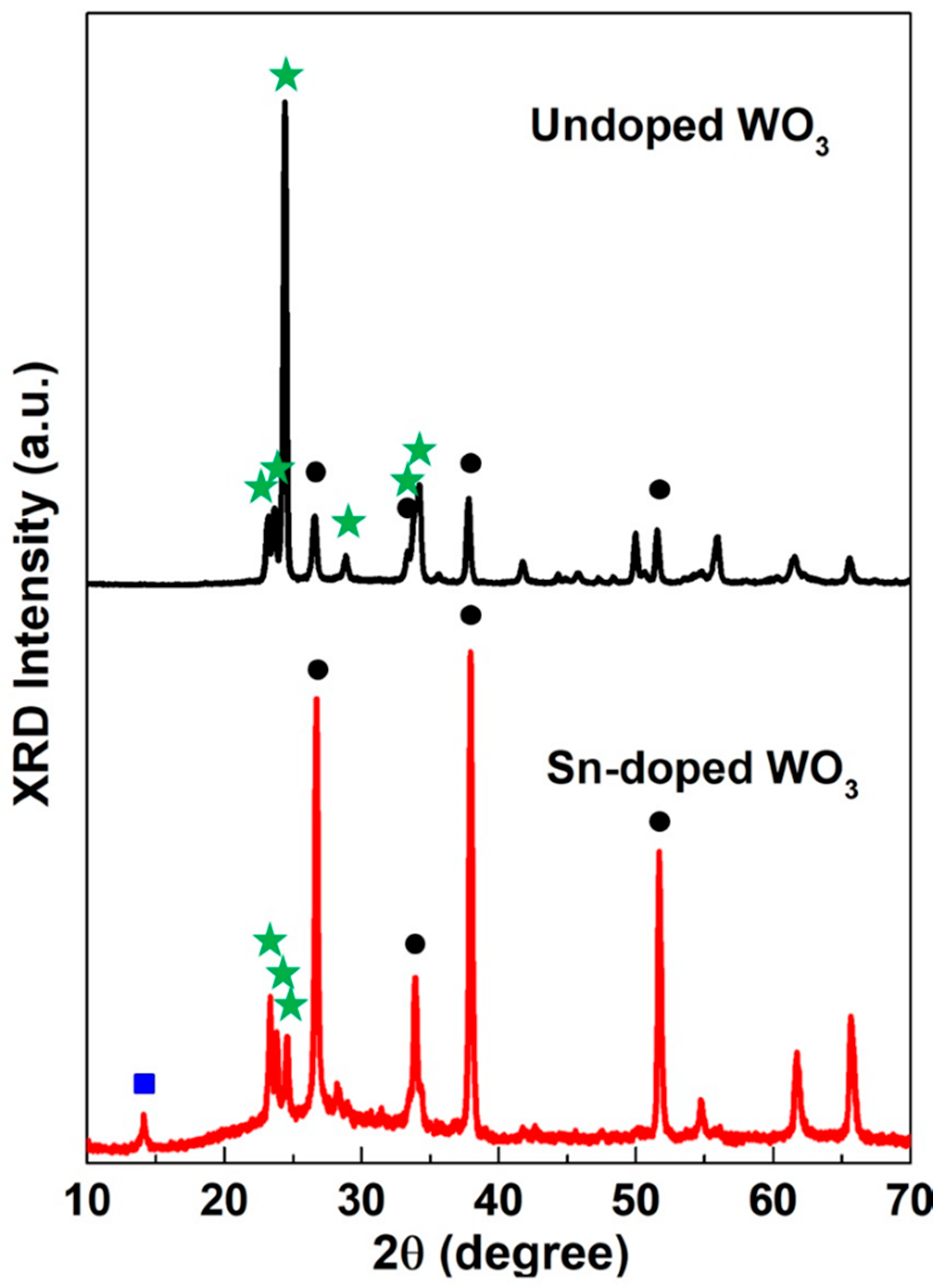
It is well known that the WO3 thin films synthesized by hydrothermal treatment of PTA solution produce orthorhombic WO3·0.33H2O that is converted to anhydrous monoclinic WO3 upon annealing at 500 °C. Figure 2a confirms that the synthesized undoped WO3 thin films (annealed at 500 °C) showed monoclinic crystal structure (with lattice parameters of a = 0.729 nm, b = 0.753 nm, c = 0.767 nm, and β = 90.92°) by producing three characteristics peaks related to [002], [020], and [200] plane at 2θ degree value of 23.18, 23.63, and 24.41 (JCPDS no. 43−1035), respectively. In Figure 2, the peaks arising from the FTO substrate (SnO2) are indicated with black dots, whereas the monoclinic peaks of WO3 are marked with green star marks. Moreover, due to the dominant appearance of substrate SnO2 peaks, the diffraction lines related to the very low concentration of doped SnO2 peaks were expected to merge and are indistinguishable. Notably, the XRD peaks of the FTO substrate appeared comparatively intense in doped WO3 compared to undoped WO3, due to the reduced thickness of WO3 film in the Sn-doped samples, as observed in Figure 1f. Careful observation of the XRD data of Sn-doped WO3 thin films (Figure 2b) revealed few critical changes in the diffraction patterns. Firstly, the peak positions of [002], [020], and [200] planes of monoclinic WO3 (with lattice parameters of a = 0.729 nm, b = 0.753 nm, c = 0.767 nm, and β = 90.92°) show a significant shift towards higher 2θ degree values. That is, the peak positions of [002], [020], and [200] planes were found to be shifted to 23.39, 23.80, and 24.56 of 2θ degree values, respectively, after Sn doping (Figure S1). This indicates that the doping of Sn takes places by displacing a few of the W ions from their lattice positions.
The most significant change observed in the XRD pattern of WO3 after Sn doping was in the peak intensities related to [002], [020], and [200] planes. The peak height associated with the different planes in the XRD pattern suggests the crystal growth direction. Interestingly, the PEC water splitting efficiency of WO3 depends on the crystal plane orientation [30]. As reported previously, a [002] plane-oriented WO3 crystal is beneficial, and performs an efficient water oxidation reaction at the surface and eventually shows higher PEC water splitting efficiency compared to the [020] and [200] plane-oriented crystals. The XRD pattern of undoped WO3 reveals the dominant and most intense peak of the [200] plane, which is reported to be a non-suitable orientation for the PEC water splitting reaction. However, upon Sn doping, a significant decrease in [200] peak and an increase in [002] was observed. This indicates that doping of Sn promotes the preferred growth direction of WO3 crystals towards the [002] orientation, from the [200] plane, and could influence its PEC water splitting efficiency. In addition to the above changes, the doping of Sn tends to induce multiple phases in WO3 as noted from the appearance of new XRD peak at a low diffraction angle, which is ascribed to the hexagonal phase of WO3. The presence of a peak related to the hexagonal phase of WO3 was due to the reconstructive transformation process that occurs during the annealing step.
As described in earlier reports, the hydrothermal treatment of PTA solution produces WO3·0.33H2O (orthorhombic phase), that undergoes a reconstructive transformation during the calcination step [31]. In particular, the reconstructive transformation involves temperature dependence, breaking of bonds, elimination of a water molecules, and a change in crystal structure with the formation of new bonds [31]. Briefly, annealing of WO3·0.33H2O at 500 °C transforms the orthorhombic phase to hexagonal phase (at 400 °C), and then to stable monoclinic phase (at 500 °C). However, the doping of Sn ions in WO3·0.33H2O (orthorhombic structure) will result in obstruction of the reconstructive transformation during calcination. Hence, the partial transformation from hexagonal to monoclinic phase takes place, resulting in multiple structures in the product. In fact, the interference of doped metal ions during reconstructive transformation, causing multiple phases of WO3, has already been observed before [16].
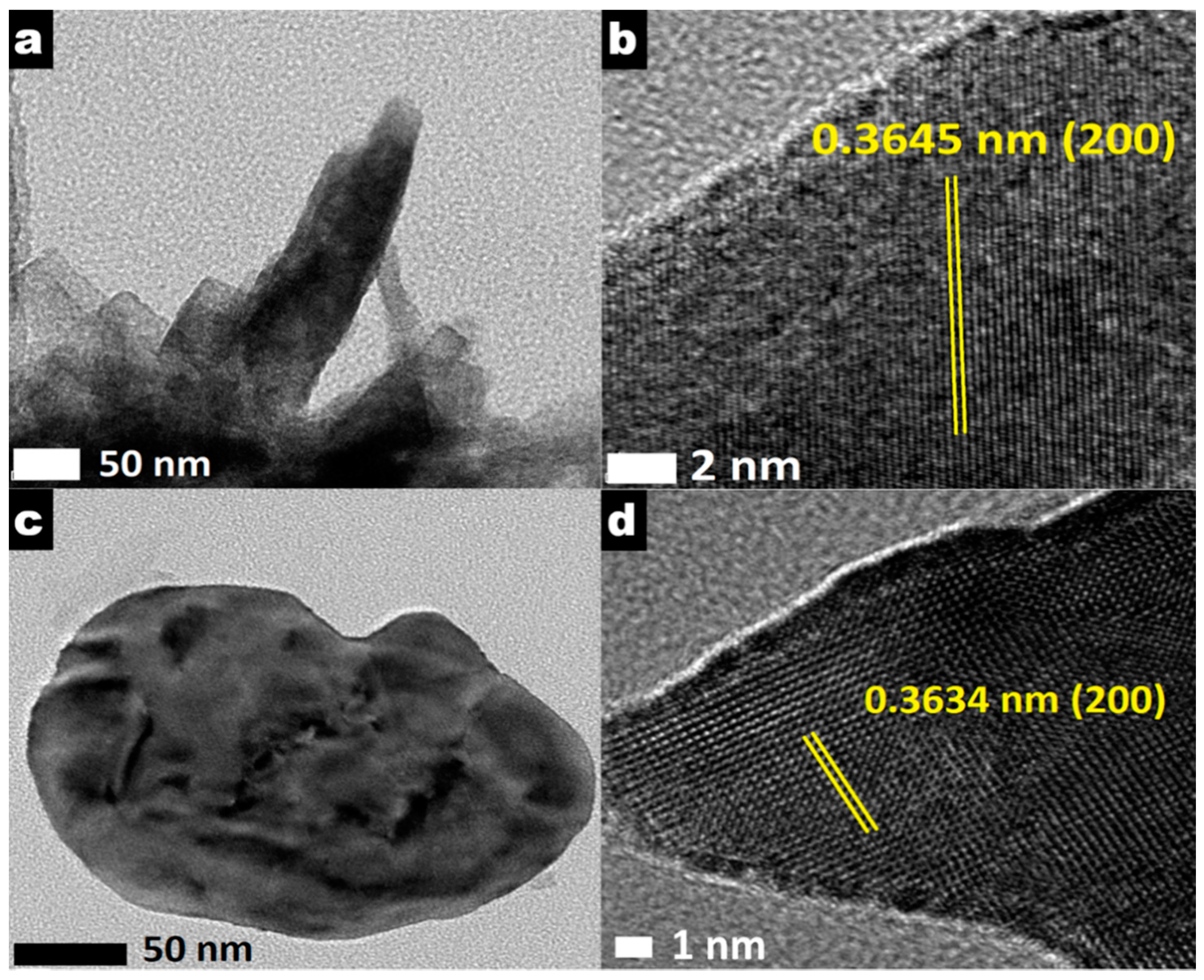
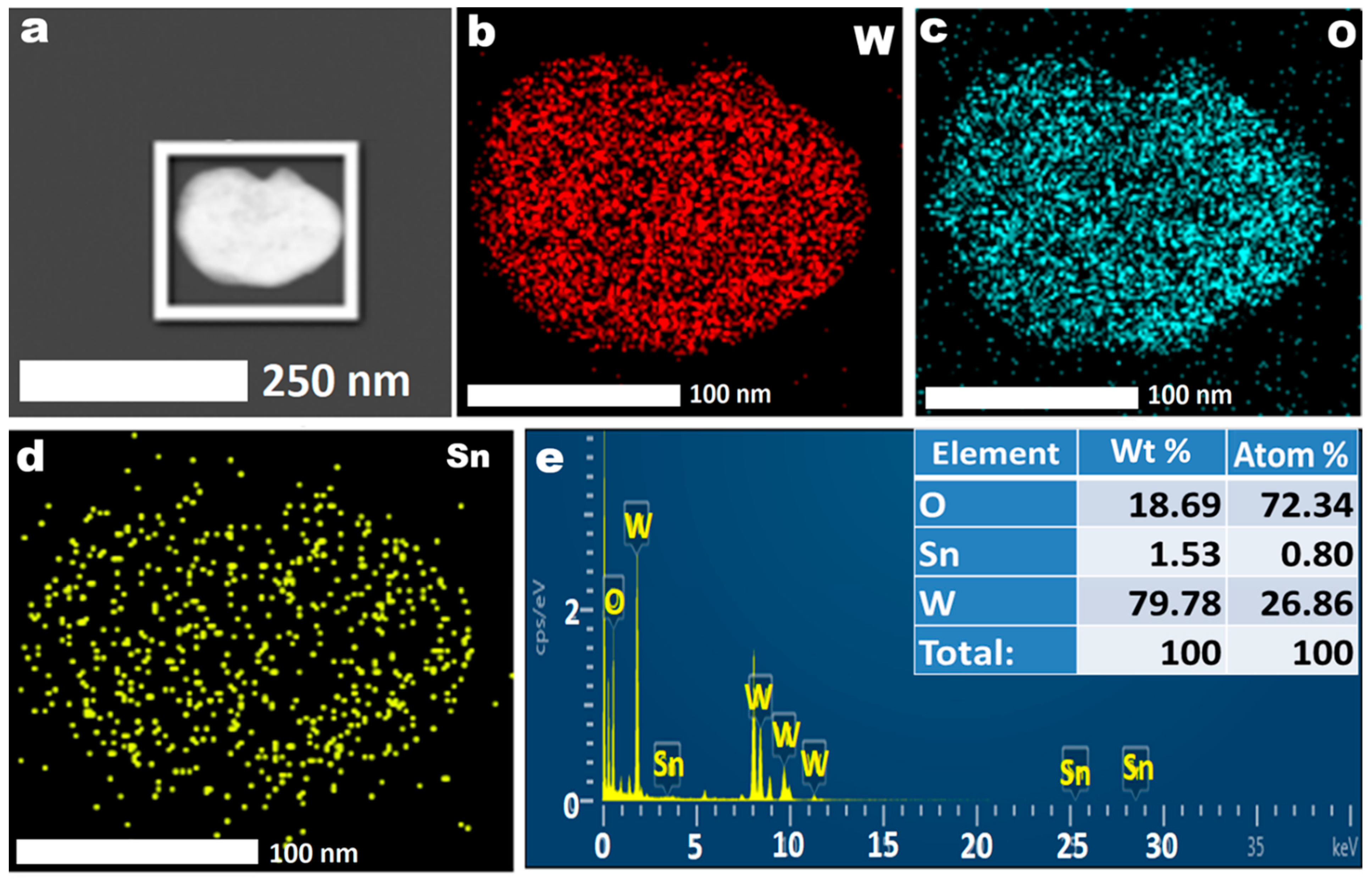
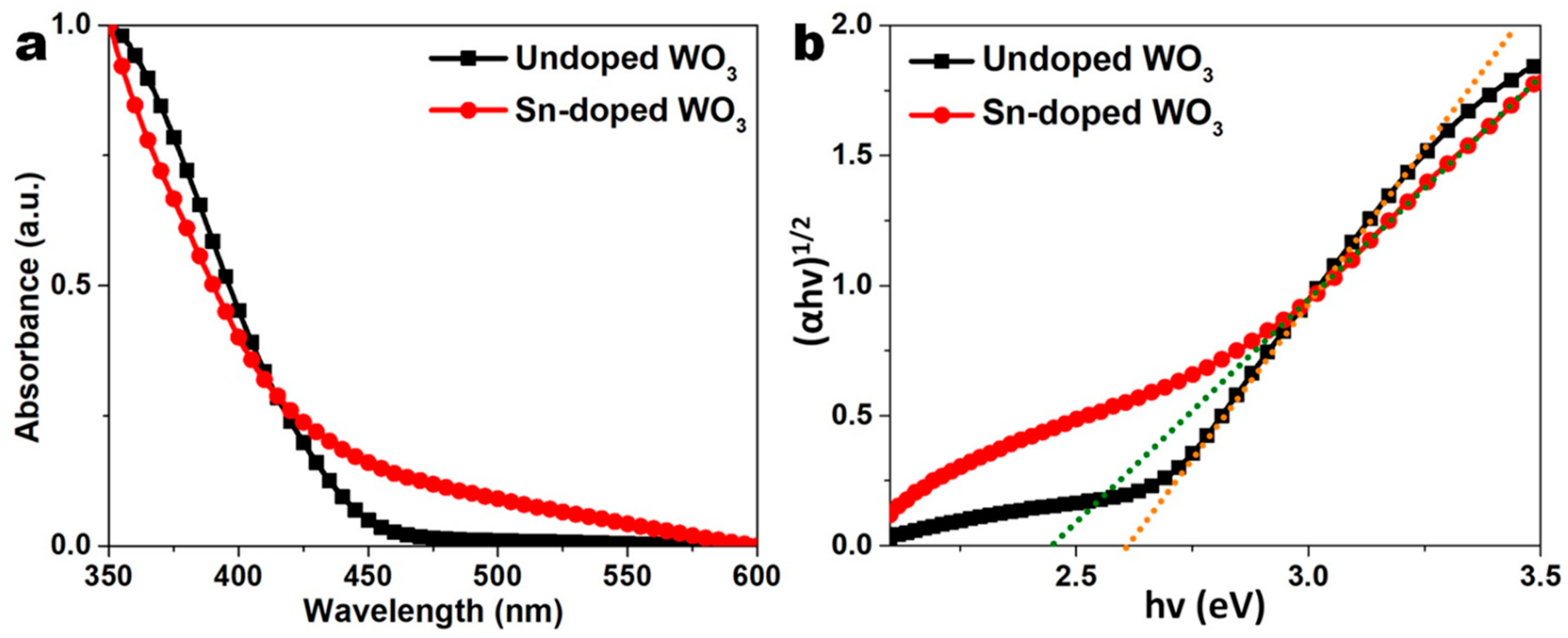
The low-resolution TEM images shown in Figure 3a,c indicate the nanorod and particle morphology of undoped and Sn-doped WO3 thin films, respectively. In the high-resolution TEM image of undoped WO3, a d-spacing value of 0.3645 was calculated (Figure 3b) which was ascribed to the [200] plane of monoclinic WO3. The d-spacing value of Sn-doped WO3 was estimated to be 0.3634 nm (Figure 3d), which was noted to be slightly less than undoped WO3. The slight decrease in d-spacing value agrees with the shift in diffraction angles to the higher degree observed in the XRD patterns after Sn doping, and hence confirms the insertion of Sn ions into the WO3 lattice. The distribution of Sn ions in WO3 lattice was observed by collecting elemental mapping data attached to the TEM. In the selected area (Figure 4a) of the Sn-doped WO3 samples, the elemental mapping showed a uniform distribution of W (Figure 4b), O (Figure 4c), and Sn (Figure 4d), and the EDS measurement (Figure 4e) confirmed atom % and wt % of individual elements and the absence of impurities. The UV–vis absorption spectra of undoped WO3 shows the absorption onset of 470 nm, as shown in Figure 5a. Upon Sn doping, a very slight redshift in absorption onset to 500 nm was observed (Figure 5a). In addition, the doping of Sn tends to cause tailing of absorbance onset into the visible region, indicating an increase in oxygen vacancies. The Tauc plot shown in Figure 5b confirms the reduction in band gap from 2.62 to 2.46 eV for undoped WO3 and Sn-doped WO3 thin films, respectively.
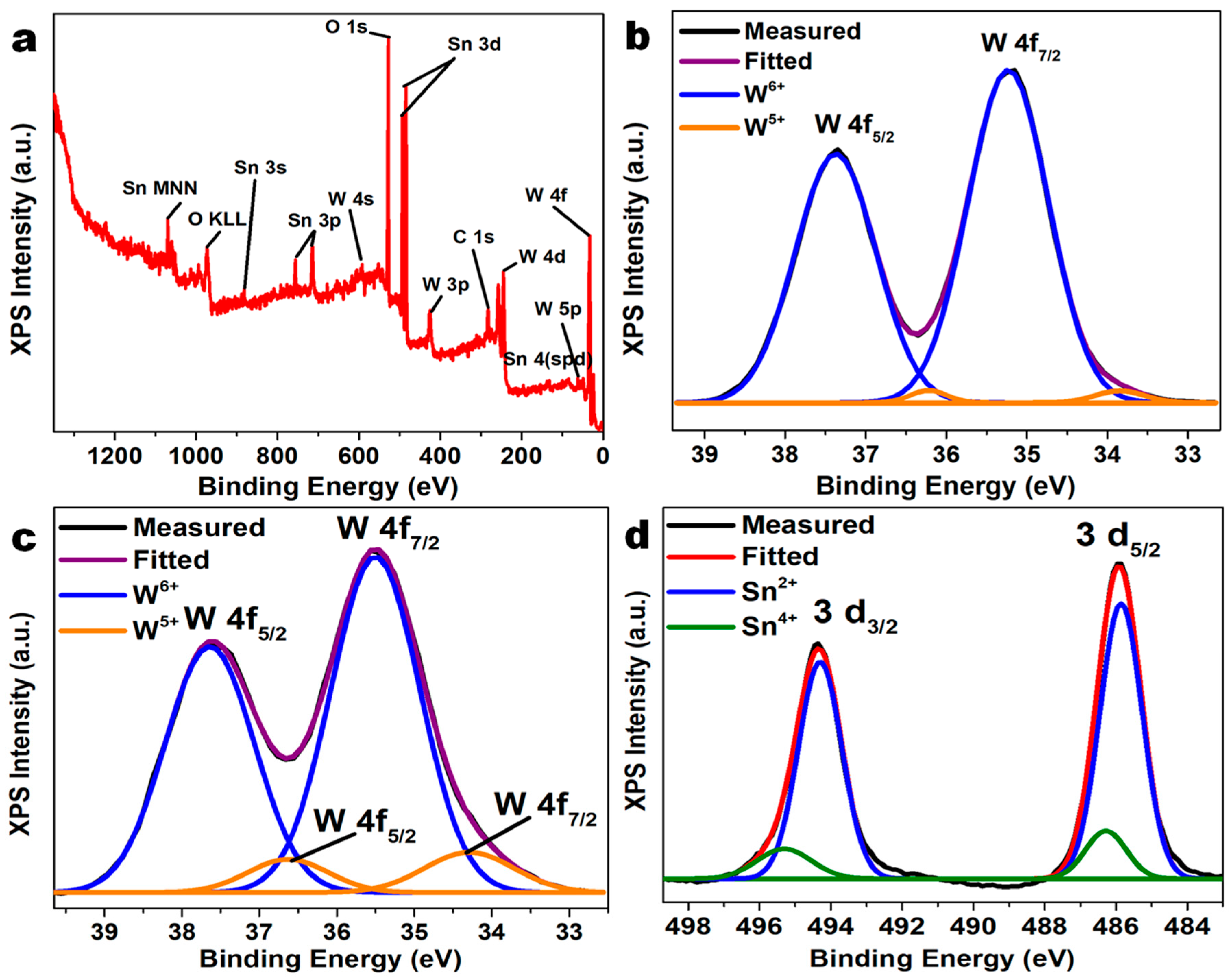
The XPS survey spectrum of Sn-doped WO3 thin films is shown in Figure 6a, indicating the presence of W, O, and Sn without any impurities. The doping of metal ions is reported to alter the concentration of oxygen vacancies in WO3. Hence, the high-resolution W 4f core-level XPS spectra were deconvoluted as shown in Figure 6b,c. In the high-resolution XPS W 4f core-level spectra, two major peaks were detected, and were assigned to W6+ state (at 35.25 and 37.40 eV of binding energy) of 4 f7/2 and 4 f5/2. In addition to the two major peaks mentioned above, two low-intensity peaks were obtained that are ascribed to the presence of W5+ state (at binding energy values of 33.95 and 36.10 eV), and hence, the presence of oxygen vacancies (i.e., causing a partial reduction of W6+) were confirmed. Similarly, the deconvolution of W 4f core-level XPS spectra of Sn-doped WO3 revealed two doublets each for W6+ and W5+ state. However, careful observation revealed that the peak intensity of W5+ state shows a significant increase after Sn doping. Precisely, the peak area of W5+ state in undoped WO3 was calculated to be 0.82% and 1.12%, corresponding to W 4f5/2 and W 4f7/2 states, respectively, and was found to be increased to 6.22% and 4.68% with respect to W 4f5/2 and W 4f7/2 state, respectively, for the Sn-doped WO3. This indicates a drastic increase in the oxygen vacancies in WO3 after Sn doping. This could be due to the change in the valence state of dopant Sn ion and the host W ions. Furthermore, in the high-resolution XPS spectra of W 4f, a significant shift in the peak positions of W6+ and W5+ states towards higher binding energy was observed. This indicates that the doping of Sn takes place by replacing W atoms via substitutional doping [32]. The high-resolution XPS spectra of Sn shows (Figure 6d) two peaks at binding energy values of 485.5 and 494.5eV, with spin–orbit components of 8.4 eV, corresponding to 3 d3/2 and 3 d5/2 core levels. Furthermore, the peak fitting deconvolution produced two doublets corresponding to the Sn(II) and Sn(IV) states. However, the presence of Sn(II) was observed to be dominant compared to the Sn(IV) state [33].
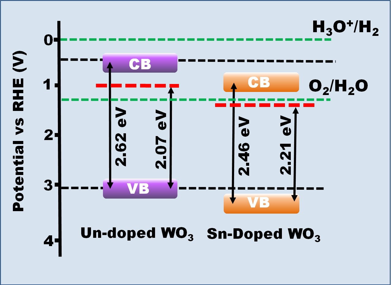
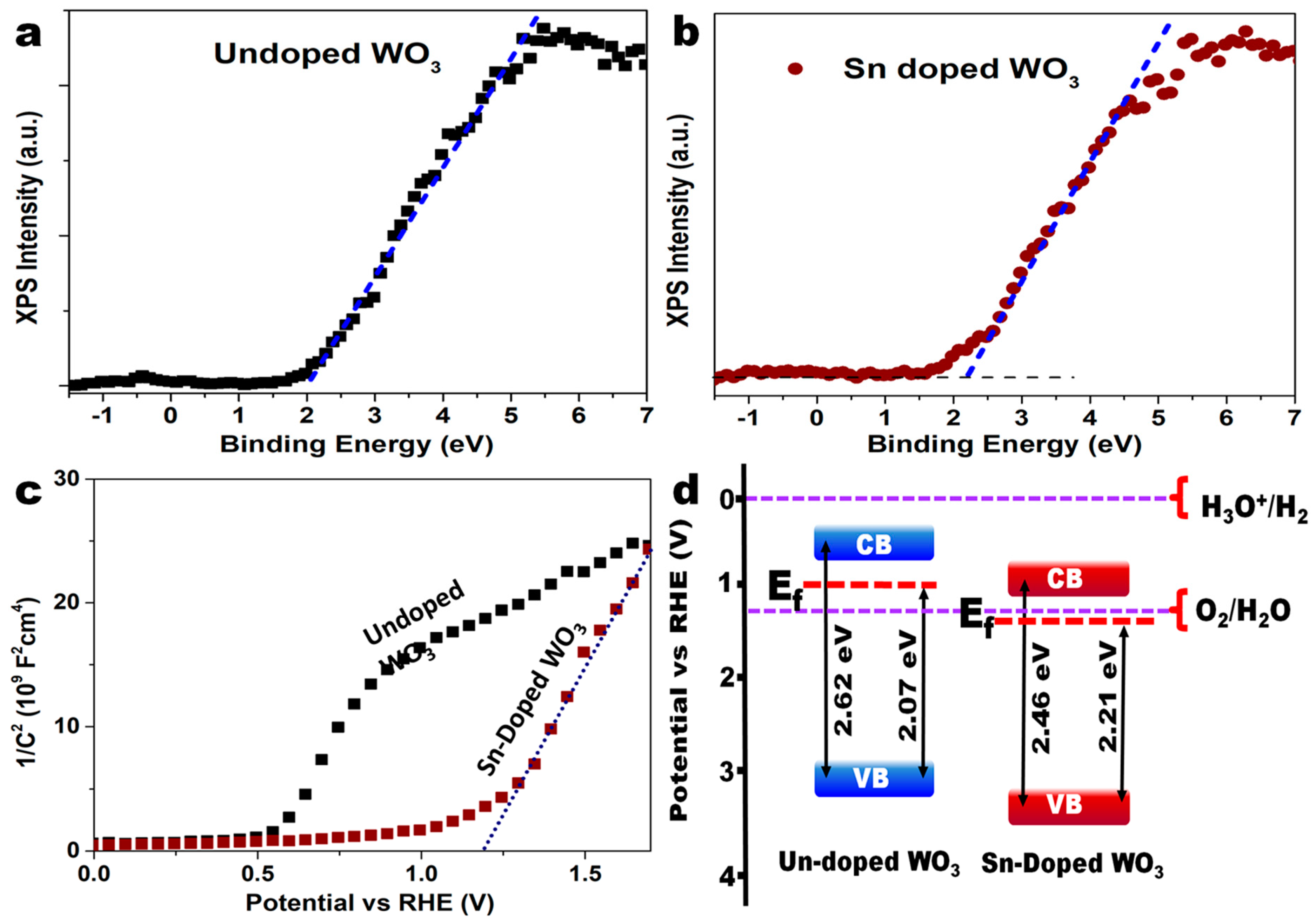
The Fermi-level position of WO3 is sensitive to its crystal environment and constituent atoms. Hence, doping WO3 tends to alter its Fermi energy level with respect to valence and conduction band edge positions. Using XPS valence band edge analysis, the energy difference between the Fermi level and the valence band edge was determined for both the undoped and Sn-doped WO3. Figure 7a,b shows the XPS valence band edge plot. The undoped WO3 show 2.07 eV energy difference between the valence band and Fermi level that increased to 2.21 eV upon Sn doping. The significant increase in energy difference tends to push the Fermi level towards and near the conduction band edge position. Hence, Sn-doped WO3 is expected to behave more n-type compared to undoped WO3.
The Mott–Schottky (MS) plot was used to understand the band edge positions of WO3 with respect to RHE values and water splitting potentials. Also, the carrier density could be determined using MS plots. The MS experiments were carried out in the dark in 0.5 M Na2SO4 at 1000 Hz of frequency using the equation
where C, ND, e, ε0, ε, VS, VFB, kB, and T are the space charge capacitance, carrier density, elementary charge, permittivity of the vacuum, the relative permittivity of WO3, applied potential, flat band potential, Boltzmann constant, and temperature (299 K), respectively. Using the slope and intercept of the plot of 1/C2 vs. applied potential (Figure 7c), ND and VFB were calculated. The VFB and ND values of undoped and Sn-doped WO3 were obtained as 0.54 V (vs. RHE), 6.35 × 1017 cm−3 and 1.21 V (vs. RHE), 8.38 × 1017 cm−3, respectively.
1/C2 = [2/(NDeε0ε)] [(VS−VFB) – (kBT/e)],
The flat band potential values obtained using MS plots suggest the position of conduction band edge position of WO3. Precisely, for the n-type semiconductors, the conduction band edge could be positioned at slightly lower potential with respect to its flat band potential [34]. Therefore, the conduction band edge of WO3 is expected to be placed at less than 0.1 V of its flat band potentials [35]. Based on the flat band edge potentials, the conduction band edge of undoped and Sn-doped WO3 was determined to be at 0.44 and 1.11 V vs. RHE, respectively. Subsequently, the positions of valence band edge position with respect to RHE were calculated using the band gap values (Figure 5) and conduction band edge positions. Figure 7d shows the band edge diagram of undoped and Sn-doped WO3 plotted against RHE values and with reference to the overall water splitting potentials. Note that the positions of Fermi levels were also included, based on the XPS results. Overall, the band edge plot indicates that the doping of Sn pushes both the conduction and valence band edge of WO3 towards higher potentials. At the same time, the Fermi level shifts upward towards the conduction band edge position, making it more n-type compared to the undoped WO3. Such an observation was evident as the doping of post-transition metal ions into WO3 shift its band edge positions towards higher potentials as previously observed in case of Bi dopant [13]. In general, it can be concluded that the doping of post-transition metal atoms into WO3 causes a downward shift in band edge positions towards higher potentials and increases the carrier density in WO3.
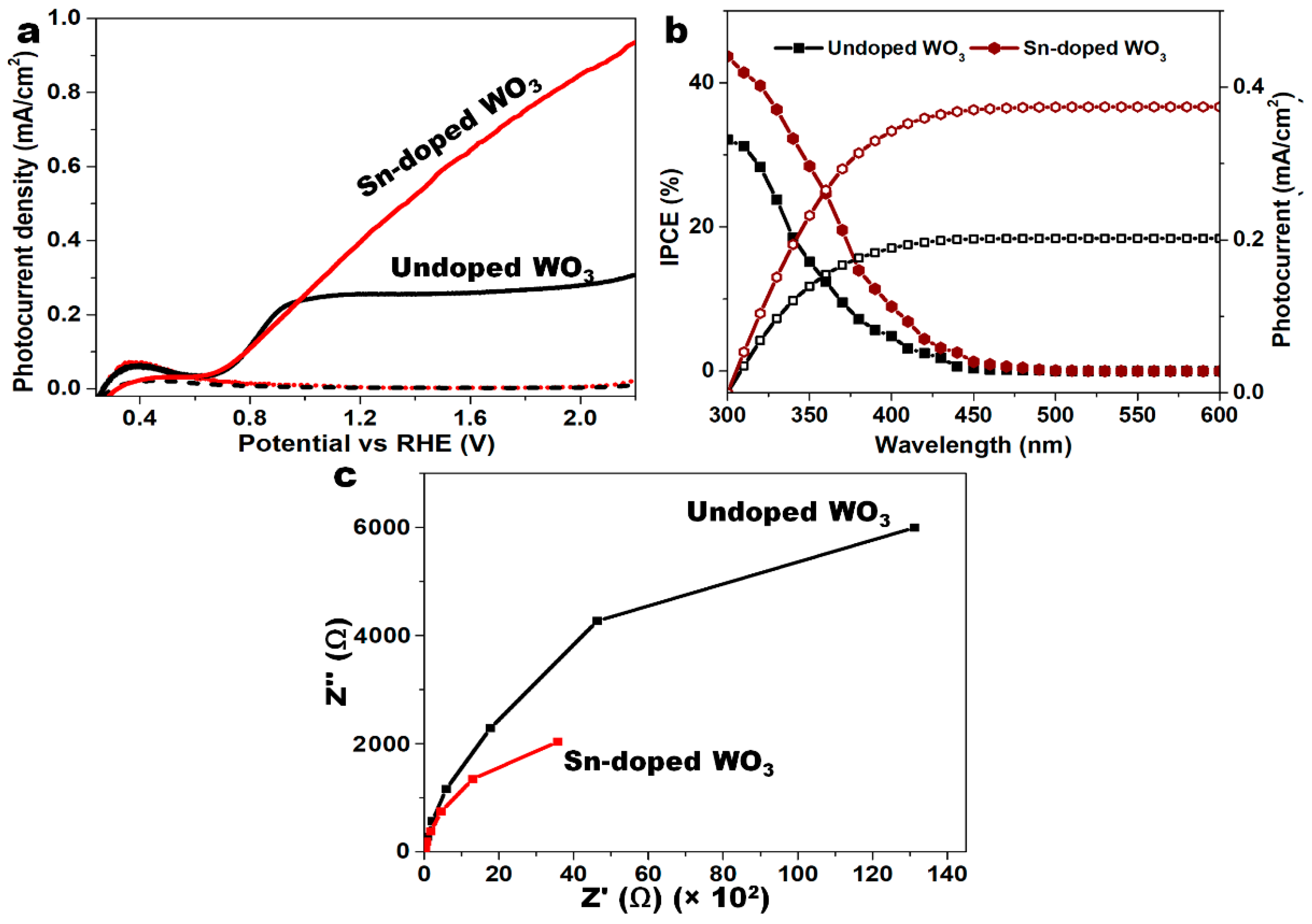
The enhancement in PEC properties of Sn-doped WO3 was evaluated by measuring linear sweep voltammetry (LSV) of doped WO3 photoanode by exposing the 1.5 G illumination in 0.5 M Na2SO4 electrolyte. Figure 8a depicts the LSV plots of undoped and Sn-doped WO3 thin films. The substitutional doping of Sn in WO3 was found to increase the photocurrent to 0.427 mA cm−2 from 0.253 mA cm−2 (at 1.23 V vs. RHE) of undoped WO3. As shown in Figure S2, the photocurrent of WO3 increases with the increase in atom % of doped Sn. The highest photocurrent was recorded at 0.80 atom % of Sn-doped WO3. The IPCE measurements were recorded to understand the PEC behavior with respect to incident light wavelength using the below equation.
where I, λ, and P refers to the current density (mA cm−2) recorded at 1.23 V vs. RHE, the wavelength of incident light (nm), and power density at a given wavelength (mW cm−2), respectively. The IPCE plots shown in Figure 8b confirm that doping of Sn increases the IPCE values to 44% (at 300 nm) along with the slight redshift of onset absorbance. This suggests that Sn-doped WO3 yields significantly higher currents than the undoped WO3 at higher wavelengths. The calculated IPCE data were integrated between the wavelength range of 300 to 600 nm using standard values of AM 1.5 G data. The integrated plots, along with the IPCE data in Figure 8b, validate the photocurrent values obtained using the solar simulator. That is, the integrated photocurrents values were in a good agreement with the values recorded in the LSV plots. Figure 8c shows Nyquist plots of the undoped and Sn-doped WO3 samples. The plots indicate that the 0.80 atom % Sn-doped WO3 shows smaller semicircle and offers lower charge transfer resistance compared to the undoped WO3 at the interface of electrode and electrolyte.
IPCE = (1240I)/(λP),
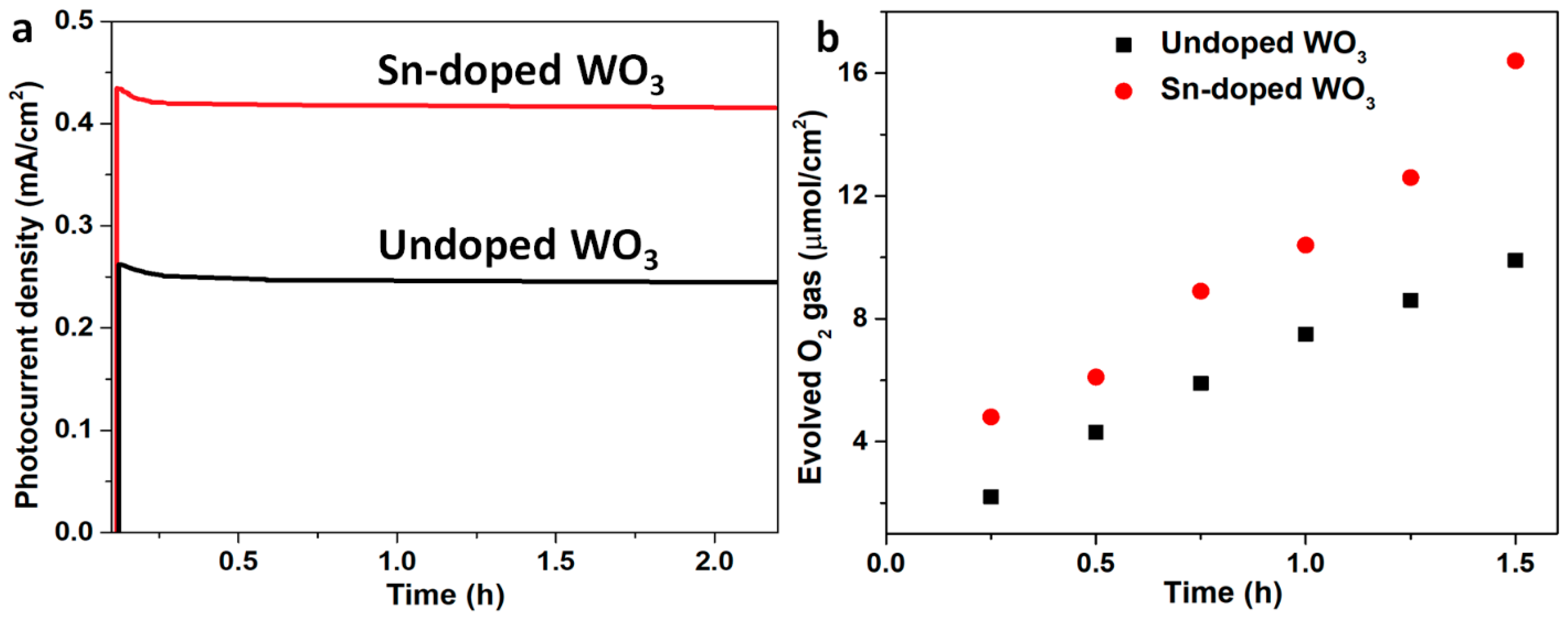
Furthermore, the stability and gas evolution amount of undoped and Sn-doped WO3 thin films were measured, and the results are shown in Figure 9. Both photoanodes exhibited good stability under continuous illumination of AM 1.5 G sunlight at a constant bias potential of 1.23 V vs. RHE (Figure 9a). This indicates that both the undoped and Sn-doped WO3 thin films show significant stability during water splitting. Moreover, the evolution of O2 gas during the water splitting were measured using GC. As shown in the Figure 9b, the Sn-doped WO3 show significant increase in the O2 evolution rate compared to the undoped WO3. Note that the valence band edge position of both undoped and Sn-doped WO3 allow the spontaneous evolution O2 gas only, and the H2 gas was not detected due to its unsuitable conduction band edge position and low level of produced photocurrents. The faradaic efficiencies for the O2 production was calculated using the following equation:
where, F, nO2, and Q are defined as the Faraday constant, amount of O2 (mol), and amount of charge (C), respectively. The faradaic efficiencies of undoped and Sn-doped WO3 were calculated to be 85% and 89%, respectively.
Faradaic efficiency = (4F × nO2)/Q,
The enhancement in PEC properties of WO3 after Sn doping was ascribed to several factors, based on the characterization results. Specifically, the orientation of crystal facet-induced band gap reduction, increase in carrier density, and the reduced charge transfer resistance were the main influencing factors for PEC activity. That is, the change in crystal facet orientation from [200] to [002] direction significantly increases water oxidation reaction kinetics at the electrode interface. This was notably evident from the impedance measurements exhibiting reduced charge transfer resistance across the interface. The optical data suggest that Sn-doped WO3 is capable of absorbing significantly more incident light compared to the undoped electrode, which also affects its photocatalytic properties. Notably, the increase in oxygen vacancies in WO3 after Sn doping extends the light-harvesting ability to the visible and near-infrared region [11]. Consequently, the increase in oxygen vacancies tends to elevate the donor density levels in WO3 as evident from the MS studies, and also improves the conductivity and enhances the PEC water splitting activities [3].
3. Materials and Methods
The thin films of Sn-doped WO3 on FTO were synthesized using an earlier reported hydrothermal method, with minor modifications [27]. The tin(II) chloride dihydrate (Sigma-Aldrich ≥99.0%, St. Louis, MI, USA) precursor was employed as the source of Sn dopant in WO3. The doping of Sn was achieved during the hydrothermal reaction of PTA solution at 150 °C (for 3 h) in the presence of Sn ions of desired concentrations. The amount of Sn dopant in WO3 was varied by controlling the concentration of tin(II) chloride dihydrate in PTA solution as described in Table S1. During the hydrothermal reaction, the FTO substrate was placed vertically in the Teflon container with its conducting side facing downwards. The synthesized undoped and doped thin films were annealed at 500 °C for 2 h. For the detailed characterization, the Sn-doped WO3 (0.80 atom %) thin film that showed the highest PEC activity was chosen.
A MiniFlex desktop XRD instrument from Rigaku (Tokyo, Japan) was used to analyze the crystalline properties of synthesized thin films between the 10° and 90° diffraction angle (2θ). The morphology and distribution of dopants in WO3 were investigated using a Hitachi S4800 (Tokyo, Japan) scanning electron microscope (SEM) and a JEOL JEM-2100F (Peabody, MA, USA) transmission electron microscope (TEM). The optical properties were explored using a Varian Cary 5000 spectrophotometer (Sydney, Australia). A Thermo Fisher Scientific (Waltham, MA, USA) instrument was utilized to analyze the valency and valence band edge properties. Linear sweep, transient and impedance measurements were carried out using an IviumStat (Eindhoven, Netherlands) electrochemical interface. The ABET Technologies Sun 2000 solar simulator (ABET Technologies, USA) calibrated to AM 1.5G was used as a light source. For IPCE measurements, a xenon arc lamp (1000 W) connected to a Thermo Oriel 66902 monochromator (Thermo Oriel Cornerstone 7400 1/8, USA) was used. The O2 gas evolved during the water splitting reaction was measured by using a YOUNG LIN YL 6500 gas chromatograph (GC) (Anyang, South Korea). Helium gas was used as a carrier medium in the capillary column, and a pulsed discharge ionization detector (PDD) was used to detect evolved O2 gas. For the PEC measurements, a three-electrode system setup was selected in a quartz cell with fabricated WO3 thin film as photoanode, Pt counter electrode, and Ag/AgCl reference electrode. All electrochemical measurements were carried out in 0.5 M Na2SO4 electrolyte. The reaction cell was thoroughly sealed, and the evolved O2 gas was fed to GC using a pump with carrier gas. For the impedance measurements under illumination, a frequency range of 0.1−105 Hz with AC voltage perturbation of 10 mV was used. The MS analysis was carried out in the dark at a frequency of 1000 Hz. The Nernst equation was used to convert the measured potential to RHE values.
4. Conclusions
Sn-doped WO3 thin films were hydrothermally synthesized, and their PEC water splitting properties were explored. The uniform and substitutional doping of Sn in the WO3 lattice was found to influence its morphology and crystal orientation. A slight reduction in the band gap was observed, along with the significant increase in the oxygen vacancies. The presence of Sn with a valency of (II) and (IV) in the WO3 lattice was confirmed via XPS studies. The MS plots revealed an anodic shift in the flat band potential and increase in the carrier densities. The band edge diagram of WO3 before and after Sn doping was plotted using XPS valence band edge, MS, and absorbance data. Based on this, a downward shift of both the valence and conduction band edge was revealed with a more n-type character of Sn-doped WO3. The PEC studies carried out in 0.5 M Na2SO4 indicated that Sn-doped WO3 performs significantly better as a photoanode than the undoped WO3. The synergic effect of Sn doping yields increased photocurrent and incident photon-to-current efficiency values. The results of this work conclude that Sn-doped WO3 performs as superior photoanode and could be utilized in performing efficient PEC water splitting. Furthermore, the scheme proposed in this article will benefit future research in fabricating more efficient WO3 photoanodes for PEC water splitting reactions.
Supplementary Materials
The following are available online at https://0-www-mdpi-com.brum.beds.ac.uk/2073-4344/9/5/456/s1, Table S1: The concentrations of tin (II) chloride dihydrate precursor added to PTA solution to obtain doped WO3 having the below atom % and wt % of Sn. Figure S1: XRD pattern of undoped and Sn-doped WO3 thin films magnified in the 2θ degree values of 21 to 26 indicating the shift in diffraction lines. Figure S2: Plot of photocurrent measured at 1.23 V vs RHE for the WO3 samples doped with various atom % of Sn.
Acknowledgments
This work was supported by the Basic Research & Development program [NRF-2017R1D1A1B03035201] of the Ministry of Science and ICT, Republic of Korea. This work was also supported by Ajou University.
Conflicts of Interest
The authors declare no conflict of interest.
References
- Datt Bhatt, M.; Sung Lee, J. Recent theoretical progress in the development of photoanode materials for solar water splitting photoelectrochemical cells. J. Mater. Chem. A 2015, 3, 10632–10659. [Google Scholar] [CrossRef]
- Walter, M.G.; Warren, E.L.; McKone, J.R.; Boettcher, S.W.; Mi, Q.; Santori, E.A.; Lewis, N.S. Solar water splitting cells. Chem. Rev. 2010, 110, 6446–6473. [Google Scholar] [CrossRef] [PubMed]
- Kalanur, S.S.; Duy, L.T.; Seo, H. Recent progress in photoelectrochemical water splitting activity of WO3 photoanodes. Top. Catal. 2018, 1–34. [Google Scholar] [CrossRef]
- Fujishima, A.; Honda, K. Electrochemical photolysis of water at a semiconductor electrode. Nature 1972, 238, 238037a0. [Google Scholar] [CrossRef]
- Di Valentin, C.; Pacchioni, G. Spectroscopic properties of doped and defective semiconducting oxides from hybrid density functional calculations. Acc. Chem. Res. 2014, 47, 3233–3241. [Google Scholar] [CrossRef] [PubMed]
- Kalanoor, B.S.; Seo, H.; Kalanur, S.S. Recent developments in photoelectrochemical water-splitting using WO3/BiVO4 heterojunction photoanode: A review. Mater. Sci. Energy Technol. 2018, 1, 49–62. [Google Scholar]
- Cahen, D.; Hodes, G.; Manassen, J. Tungsten trioxide as a photoanode for a photoelectrochemical cell (PEC). Nature 1976, 260, 312. [Google Scholar]
- Liu, X.; Wang, F.; Wang, Q. Nanostructure-based WO3 photoanodes for photoelectrochemical water splitting. Phys. Chem. Chem. Phys. 2012, 14, 7894–7911. [Google Scholar] [CrossRef] [PubMed]
- Song, J.; Huang, Z.-F.; Pan, L.; Zou, J.-J.; Zhang, X.; Wang, L. Oxygen-deficient tungsten oxide as versatile and efficient hydrogenation catalyst. ACS Catal. 2015, 5, 6594–6599. [Google Scholar] [CrossRef]
- Huang, Z.-F.; Song, J.; Pan, L.; Zhang, X.; Wang, L.; Zou, J.-J. Tungsten oxides for photocatalysis, electrochemistry, and phototherapy. Adv. Mater. 2015, 27, 5309–5327. [Google Scholar] [CrossRef]
- Kalanur, S.S.; Yoo, I.-H.; Cho, I.-S.; Seo, H. Effect of oxygen vacancies on the band edge properties of WO3 producing enhanced photocurrents. Electrochimica Acta 2019, 296, 517–527. [Google Scholar] [CrossRef]
- Upadhyay, S.B.; Mishra, R.K.; Sahay, P.P. Structural and alcohol response characteristics of Sn-doped WO3 nanosheets. Sens. Actuators B Chem. 2014, 193, 19–27. [Google Scholar] [CrossRef]
- Kalanur, S.S.; Yoo, I.-H.; Eom, K.; Seo, H. Enhancement of photoelectrochemical water splitting response of WO3 by Means of Bi doping. J. Catal. 2018, 357, 127–137. [Google Scholar] [CrossRef]
- Wang, F.; Di Valentin, C.; Pacchioni, G. Electronic and structural properties of WO3: A systematic hybrid DFT study. J. Phys. Chem. C 2011, 115, 8345–8353. [Google Scholar] [CrossRef]
- Wang, F.; Di Valentin, C.; Pacchioni, G. Doping of WO3 for photocatalytic water splitting: hints from density functional theory. J. Phys. Chem. C 2012, 116, 8901–8909. [Google Scholar] [CrossRef]
- Kalanur, S.S.; Yoo, I.-H.; Seo, H. Fundamental investigation of Ti doped WO3 photoanode and their influence on photoelectrochemical water splitting activity. Electrochimica Acta 2017, 254, 348–357. [Google Scholar] [CrossRef]
- Kalanur, S.S.; Seo, H. Influence of molybdenum doping on the structural, optical and electronic properties of WO3 for improved solar water splitting. J. Colloid Interface Sci. 2018, 509, 440–447. [Google Scholar] [CrossRef]
- Hameed, A.; Gondal, M.A.; Yamani, Z.H. Effect of transition metal doping on photocatalytic activity of WO3 for water splitting under laser illumination: role of 3d-orbitals. Catal. Commun. 2004, 5, 715–719. [Google Scholar] [CrossRef]
- Cheng, X.F.; Leng, W.H.; Liu, D.P.; Zhang, J.Q.; Cao, C.N. Enhanced photoelectrocatalytic performance of Zn-doped WO3 photocatalysts for nitrite ions degradation under visible light. Chemosphere 2007, 68, 1976–1984. [Google Scholar] [CrossRef]
- Kalanur, S.S.; Yoo, I.-H.; Cho, I.S.; Seo, H. Niobium incorporated WO3 nanotriangles: Band edge insights and improved photoelectrochemical water splitting activity. Ceram. Int. 2019. [Google Scholar] [CrossRef]
- Li, W.; Zhan, F.; Li, J.; Liu, C.; Yang, Y.; Li, Y.; Chen, Q. Enhancing photoelectrochemical water splitting by aluminum-doped plate-like WO3 electrodes. Electrochimica Acta 2015, 160, 57–63. [Google Scholar] [CrossRef]
- Kalanur, S.S.; Seo, H. Aligned nanotriangles of tantalum doped tungsten oxide for improved photoelectrochemical water splitting. J. Alloys Compd. 2019, 785, 1097–1105. [Google Scholar] [CrossRef]
- Zhang, T.; Zhu, Z.; Chen, H.; Bai, Y.; Xiao, S.; Zheng, X.; Xue, Q.; Yang, S. Iron-doping-enhanced photoelectrochemical water splitting performance of nanostructured WO3: a combined experimental and theoretical study. Nanoscale 2015, 7, 2933–2940. [Google Scholar] [CrossRef] [PubMed]
- Han, S.; Li, J.; Chen, X.; Huang, Y.; Liu, C.; Yang, Y.; Li, W. Enhancing photoelectrochemical activity of nanocrystalline WO3 electrodes by surface tuning with Fe(III). Int. J. Hydrog. Energy 2012, 37, 16810–16816. [Google Scholar] [CrossRef]
- Song, H.; Li, Y.; Lou, Z.; Xiao, M.; Hu, L.; Ye, Z.; Zhu, L. Synthesis of Fe-doped WO3 nanostructures with high visible-light-driven photocatalytic activities. Appl. Catal. B Environ. 2015, 166–167, 112–120. [Google Scholar] [CrossRef]
- Yang, B.; Luca, V. Enhanced long-wavelength transient photoresponsiveness of WO3 induced by tellurium doping. Chem. Commun. 2008, 4454–4456. [Google Scholar] [CrossRef]
- Kalanur, S.S.; Seo, H. Intercalation of barium into monoclinic tungsten oxide nanoplates for enhanced photoelectrochemical water splitting. Chem. Eng. J. 2019, 355, 784–796. [Google Scholar] [CrossRef]
- Cai, J.; Li, S.; Li, Z.; Wang, J.; Ren, Y.; Qin, G. Electrodeposition of Sn-doped hollow α-Fe2O3 nanostructures for photoelectrochemical water splitting. J. Alloys Compd. 2013, 574, 421–426. [Google Scholar] [CrossRef]
- Zhou, Z.; Wu, S.; Qin, L.; Li, L.; Li, L.; Li, X. Modulating oxygen vacancies in Sn-doped hematite film grown on silicon microwires for photoelectrochemical water oxidation. J. Mater. Chem. A 2018, 6, 15593–15602. [Google Scholar] [CrossRef]
- Songcan, W.; Hongjun, C.; Guoping, G.; Teera, B.; Miaoqiang, L.; Supphasin, T.; Jung-Ho, Y.; Aijun, D.; Gang, L.; Lianzhou, W. Synergistic crystal facet engineering and structural control of WO3 films exhibiting unprecedented photoelectrochemical performance. Nano Energy 2016, 24, 94–102. [Google Scholar]
- Kalanur, S.S.; Hwang, Y.J.; Chae, S.Y.; Joo, O.S. Facile growth of aligned WO3 nanorods on FTO substrate for enhanced photoanodic water oxidation activity. J. Mater. Chem. A 2013, 1, 3479–3488. [Google Scholar] [CrossRef]
- Qi, J.; Chen, K.; Xing, Y.; Fan, H.; Zhao, H.; Yang, J.; Li, L.; Yan, B.; Zhou, J.; Guo, L.; et al. Application of 3D hierarchical monoclinic-type structural Sb-doped WO3 towards NO2 gas detection at low temperature. Nanoscale 2018, 10, 7440–7450. [Google Scholar] [CrossRef] [PubMed]
- Xia, W.; Wang, H.; Zeng, X.; Han, J.; Zhu, J.; Zhou, M.; Wu, S. High-efficiency photocatalytic activity of type II SnO/Sn3O4 heterostructures via interfacial charge transfer. Cryst. Eng. Comm. 2014, 16, 6841–6847. [Google Scholar] [CrossRef]
- Matsumoto, Y.; Omae, M.; Watanabe, I.; Sato, E. Photoelectrochemical properties of the Zn-Ti-Fe spinel oxides. J. Electrochem. Soc. 1986, 133, 711–716. [Google Scholar] [CrossRef]
- Guo, W.; Chemelewski, W.D.; Mabayoje, O.; Xiao, P.; Zhang, Y.; Mullins, C.B. Synthesis and characterization of CuV2O6 and Cu2V2O7: Two photoanode candidates for photoelectrochemical water oxidation. J. Phys. Chem. C 2015, 119, 27220–27227. [Google Scholar] [CrossRef]
Figure 1.
Low (a,d) and high (b,e) resolution surface and (c,f) cross-section SEM images of undoped and Sn-doped WO3, respectively.
Figure 1.
Low (a,d) and high (b,e) resolution surface and (c,f) cross-section SEM images of undoped and Sn-doped WO3, respectively.

Figure 2.
XRD patterns of undoped and Sn-doped WO3 thin films. The XRD peaks of FTO substrate and monoclinic and hexagonal WO3 are indicated by a dot (black), star (green) and square (blue) marks.
Figure 2.
XRD patterns of undoped and Sn-doped WO3 thin films. The XRD peaks of FTO substrate and monoclinic and hexagonal WO3 are indicated by a dot (black), star (green) and square (blue) marks.

Figure 3.
Low (a) and high (b) resolution TEM images of undoped WO3 showing the d-spacing value of 0.3645 nm ascribed to [200] plane of monoclinic WO3. (c) Low- and (d) high-resolution TEM image of Sn-doped WO3 exhibiting the d-spacing value of 0.3634 nm.
Figure 3.
Low (a) and high (b) resolution TEM images of undoped WO3 showing the d-spacing value of 0.3645 nm ascribed to [200] plane of monoclinic WO3. (c) Low- and (d) high-resolution TEM image of Sn-doped WO3 exhibiting the d-spacing value of 0.3634 nm.

Figure 4.
(a) Scanning transmission electron microscopy (STEM) image showing the selected area of Sn-doped WO3 nanoparticle and elemental mapping indicating the distribution of (b) W, (c) O, and (d) Sn. (e) EDS graph and the inset table show the quantitative values of elements present in the Sn-doped WO3 nanoparticle.

Figure 5.
(a) UV–vis absorption spectra and (b) Tauc plot of undoped (black) and Sn-doped WO3 (red) thin films.
Figure 5.
(a) UV–vis absorption spectra and (b) Tauc plot of undoped (black) and Sn-doped WO3 (red) thin films.

Figure 6.
(a) XPS survey spectrum of the Sn-doped WO3 thin film. Deconvoluted high-resolution XPS spectra of W 4f core level of (b) undoped and (c) Sn-doped WO3. (d) Deconvoluted high-resolution XPS spectra of Sn 3d core levels.
Figure 6.
(a) XPS survey spectrum of the Sn-doped WO3 thin film. Deconvoluted high-resolution XPS spectra of W 4f core level of (b) undoped and (c) Sn-doped WO3. (d) Deconvoluted high-resolution XPS spectra of Sn 3d core levels.

Figure 7.
XPS valence band edge plot of (a) undoped and (b) Sn-doped WO3 thin films. (c) Mott–Schottky plot of undoped and Sn-doped WO3 thin films. (d) Band edge position of WO3 plotted against RHE before and after doping with Sn.
Figure 7.
XPS valence band edge plot of (a) undoped and (b) Sn-doped WO3 thin films. (c) Mott–Schottky plot of undoped and Sn-doped WO3 thin films. (d) Band edge position of WO3 plotted against RHE before and after doping with Sn.

Figure 8.
(a) Linear sweep voltammetry (LSV) plots (dotted lines indicated LSV measured in the dark), (b) incident photon-to-current efficiency (IPCE) and integrated IPCE, and (c) Nyquist plots of the undoped and Sn-doped WO3 thin films measured in 0.5 M Na2SO4.
Figure 8.
(a) Linear sweep voltammetry (LSV) plots (dotted lines indicated LSV measured in the dark), (b) incident photon-to-current efficiency (IPCE) and integrated IPCE, and (c) Nyquist plots of the undoped and Sn-doped WO3 thin films measured in 0.5 M Na2SO4.

Figure 9.
(a) Transient voltammogram of undoped and Sn-doped WO3 thin films measured under AM 1.5 G illumination at an applied bias potential of 1.23 V RHE. (b) The evolution of O2 gas at the photoanode measured for undoped and Sn-doped WO3 under AM 1.5 G illumination at an applied bias potential of 1.23 V RHE using GC.

© 2019 by the author. Licensee MDPI, Basel, Switzerland. This article is an open access article distributed under the terms and conditions of the Creative Commons Attribution (CC BY) license (http://creativecommons.org/licenses/by/4.0/).
Share and Cite
MDPI and ACS Style
Kalanur, S.S. Structural, Optical, Band Edge and Enhanced Photoelectrochemical Water Splitting Properties of Tin-Doped WO3. Catalysts 2019, 9, 456. https://0-doi-org.brum.beds.ac.uk/10.3390/catal9050456
AMA Style
Kalanur SS. Structural, Optical, Band Edge and Enhanced Photoelectrochemical Water Splitting Properties of Tin-Doped WO3. Catalysts. 2019; 9(5):456. https://0-doi-org.brum.beds.ac.uk/10.3390/catal9050456
Chicago/Turabian StyleKalanur, Shankara S. 2019. "Structural, Optical, Band Edge and Enhanced Photoelectrochemical Water Splitting Properties of Tin-Doped WO3" Catalysts 9, no. 5: 456. https://0-doi-org.brum.beds.ac.uk/10.3390/catal9050456
Note that from the first issue of 2016, this journal uses article numbers instead of page numbers. See further details here.