Transfer of Graphene with Protective Oxide Layers
by
 ,
,
Haim Grebel
1,*, 
Liliana Stan
2,
Anirudha V. Sumant
2,
Yuzi Liu
2,
David Gosztola
2,
Leonidas Ocola
2 and
Brandon Fisher
2 1
Electronic Imaging Center and ECE Department, New Jersey Institute of Technology (NJIT), Newark, NJ 07102, USA
2
Center for Nanoscale Materials, Nanoscience and Technology Division, Argonne National Laboratory, Argonne, IL 60439, USA
*
Author to whom correspondence should be addressed.
ChemEngineering 2018, 2(4), 58; https://0-doi-org.brum.beds.ac.uk/10.3390/chemengineering2040058
Submission received: 15 October 2018
/
Revised: 9 November 2018
/
Accepted: 19 November 2018
/
Published: 3 December 2018
(This article belongs to the Special Issue Advanced Functional Low-dimensional Materials and Their Applications)
Abstract
:Transfer of graphene, grown by chemical vapor deposition (CVD), to a substrate of choice, typically involves the deposition of a polymeric layer (for example, poly(methyl methacrylate) (PMMA), or polydimethylsiloxane, PDMS). These polymers are quite hard to remove without leaving some residues behind. One method to improve the graphene transfer is to coat the graphene with a thin protective oxide layer, followed by the deposition of a very thin polymer layer on top of the oxide layer (much thinner than the usual thickness), followed by a more aggressive polymeric removal method, thus leaving the graphene intact. At the same time, having an oxide layer on graphene may serve applications, such as channeled transistors or sensing devices. Here, we study the transfer of graphene with a protective thin oxide layer grown by atomic layer deposition (ALD). We follow the transfer process from the graphene growth stage through oxide deposition until completion. We report on the nucleation growth process of oxides on graphene, their resultant strain and their optical transmission.
1. Introduction
The typical transfer of graphene—grown by chemical vapor deposition (CVD) on Cu or Ni substrates—onto a substrate of choice, involves some intermediate stages [1,2,3,4,5,6,7,8,9]. The graphene-deposited metal substrate is typically coated with a polymer, for example, poly(methyl methacrylate) (PMMA) [1], or polydimethylsiloxane (PDMS) [2], in order to protect it through the following transfer stages. The metal films are etched away and the graphene/polymer film is transferred onto and left to rest on the desired substrate. The polymer is later removed by dissolving it out, or peeling it off. Any aggressive polymer removal method, such as reactive ion etching, is prohibited for fear of damaging the graphene layer. The polymer deposition step is problematic because remnants of the polymer may be left behind and impede the following processing stages. At the same time, many applications, for example, graphene-based channel transistors and sensing devices, require a top gate oxide layer.
The growth of the oxide on the graphene poses some problems, though. Pinholes, poor adhesion and non-uniformity are attributed to the chemically inert graphene because its surface lacks dangling bonds to assist the adhesion process. Nevertheless, several groups have been able, using the atomic layer deposition (ALD) technique, to deposit thin and continuous HfO2 or Al2O3 layers on graphene [10,11,12,13]. In order to improve the nucleation of the dielectric on graphene and obtain smooth uniform films, several graphene surface pretreatment methods prior to ALD have been used, for example, the deposition of a thin metal seed layer [14] or polymer films [10,15,16] or pretreatment of the graphene surface with ozone [17,18]. Other groups demonstrated new methods of improving the ALD dielectric nucleation on graphene without the assistance of a transition layer or surface functionalization: (a) By controlling gas−solid physical adsorption between water molecules and graphene through the optimization of H2O pre-treatment and two-step temperature growth [19] or (b) by tuning graphene surface energy using the metal substrate to create polar traps and nucleation sites on the graphene surface [12,20].
Considering that the graphene may be protected by a top oxide layer throughout the transfer stages, we performed a systematic study of the transfer of a CVD grown graphene with a layer of protective oxide, i.e., alumina (Al2O3) and hafnia (HfO2) deposited by ALD. Moreover, depositing the oxide layers before transferring the graphene may result in higher quality oxide, due to the ability of improving the oxide nucleation by tuning the graphene surface energy and allowing a more efficient trapping of water molecules [21].
2. Experiment and Initial Characterization
The 25 micron thick Cu foil substrate, used in the graphene growth process has a template-like pattern, remnant of its manufacturing, which is apparent upon the deposition of oxides. This pattern is invisible when transferring the graphene with only PMMA; either because it is relieved or because of film transparency. The template in the Cu foil during extrusion could result in the further straining of the graphene layer and in principle, one may use flat Ni or Cu films on Si/SiO2, instead [2]. Nevertheless, the stress related impact of such patterns is rather small. Graphene was grown by using a commercial Thermal CVD system (Atomate Corp., Simi Valley, CA, USA). The process starts by annealing a bare Cu foil in a hydrogen atmosphere. It follows with graphene growth at a high temperature (1000 °C) using methane flow (50 sccm) as a carbon source at intermediate pressure (1 Torr) for a few minutes. The process is concluded by cooling from growth temperature to room temperature in a hydrogen atmosphere (300 Torr). This results in mostly bi-layer graphene on Cu foil [22], albeit, Raman spectra reveal areas with single layers, as well.
Aluminum oxide (alumina, Al2O3) and hafnium oxide (hafnia, HfO2) were deposited by Atomic Layer Deposition in an Arradiance Gemstar system using a two-step growth process [10,11,12]. For the Al2O3 films, trimethylaluminum (TMA, STREM Chemicals) was used as a precursor and water as an oxidant and for the HfO2 films, tetrakis(ethylmethylamino)hafnium (TEMAH, STREM Chemicals) was used as a precursor and H2O as an oxidant. The TEMAH precursor was heated to 95 °C with a heating jacket, while the water was kept at room temperature. High purity nitrogen gas (99.999%) was used as a carrying and purging gas with a flow rate of 40 sccm and 100 sccm, respectively. During the high exposure-mode ALD process, the evacuation valve was closed before introducing the precursor in the chamber and opened after a delay time. In the first step, a seed layer (3 cycles for both, Al2O3 and HfO2) was grown at lower temperature (90 °C). During the seed layer growth, 3 pulses of water, 0.022 s each were followed by 1 pulse of the metal precursor (0.022 s TMA and 1 s TEMAH, respectively). The usage of more water than for a conventional ALD process during this low temperature step was intended to facilitate the adherence of water to the graphene through physical absorption [20]. The second step was the bulk layer growth (100 cycles) at higher temperature (200 °C). An Al2O3 cycle consisted of 0.022 s TMA pulse, 1 s delay, 28 s N2 purge, 0.022 s H2O pulse, 1 s delay, and 28 s N2 purge. An HfO2 cycle consisted of 1 s TEMAH pulse, 2 s delay, 28 s N2 purge, 0.022 s H2O pulse, 1 s delay, and 34 s N2 purge. The resulting Al2O3 and HfO2 films had a thickness of about 10 nm.
The transfer of the 10-nm oxide-graphene layer was made by either a direct transfer or aided by depositing the oxide-graphene layer with an additional, ca 50 nm thick, PMMA film. A direct transfer means that the copper substrate is etched and the film is floating in de-ionized (DI) water prior to scooping it up on the substrate (a glass slide or thermally oxidized silicon wafer). In the second approach, a 50-nm PMMA is spun over the oxide-graphene film while on the copper foil. The PMMA film is invisible on a glass slide but has a bluish taint when deposited on a 50-nm thick oxide on a Si wafer. Transferring only the oxide (without the graphene) is near impossible because the oxide disintegrates while floating on the DI water on its own. The graphene is strong enough to hold the oxide-graphene film together. The addition of the PMMA film, on top of the oxide-graphene film makes the transfer process much easier and results in less fragile film. We used acetone at 40 °C or Anisole at RT to remove the extra PMMA on oxide. The additionally deposited PMMA film is much thinner than a typical PMMA film used for graphene transfer—a 50-nm thick film compared with a typical thickness of 150-nm and need not be heated thoroughly (less than 1 min on a 180 °C hot plate or as low as 1 min on a 60 °C plate, compared with >3 min on a 180 °C plate).
Scanning electron microscopy (SEM) pictures of 10-nm alumina and 10-nm hafnia on bare Cu are shown in Figure 1. The coverage of the oxide film is rather uniform on the Cu foil and is consistent with earlier studies [23]. This is probably because the oxide growth step involves water, which partially oxidizes the copper surface and enables a more homogeneous nucleation.
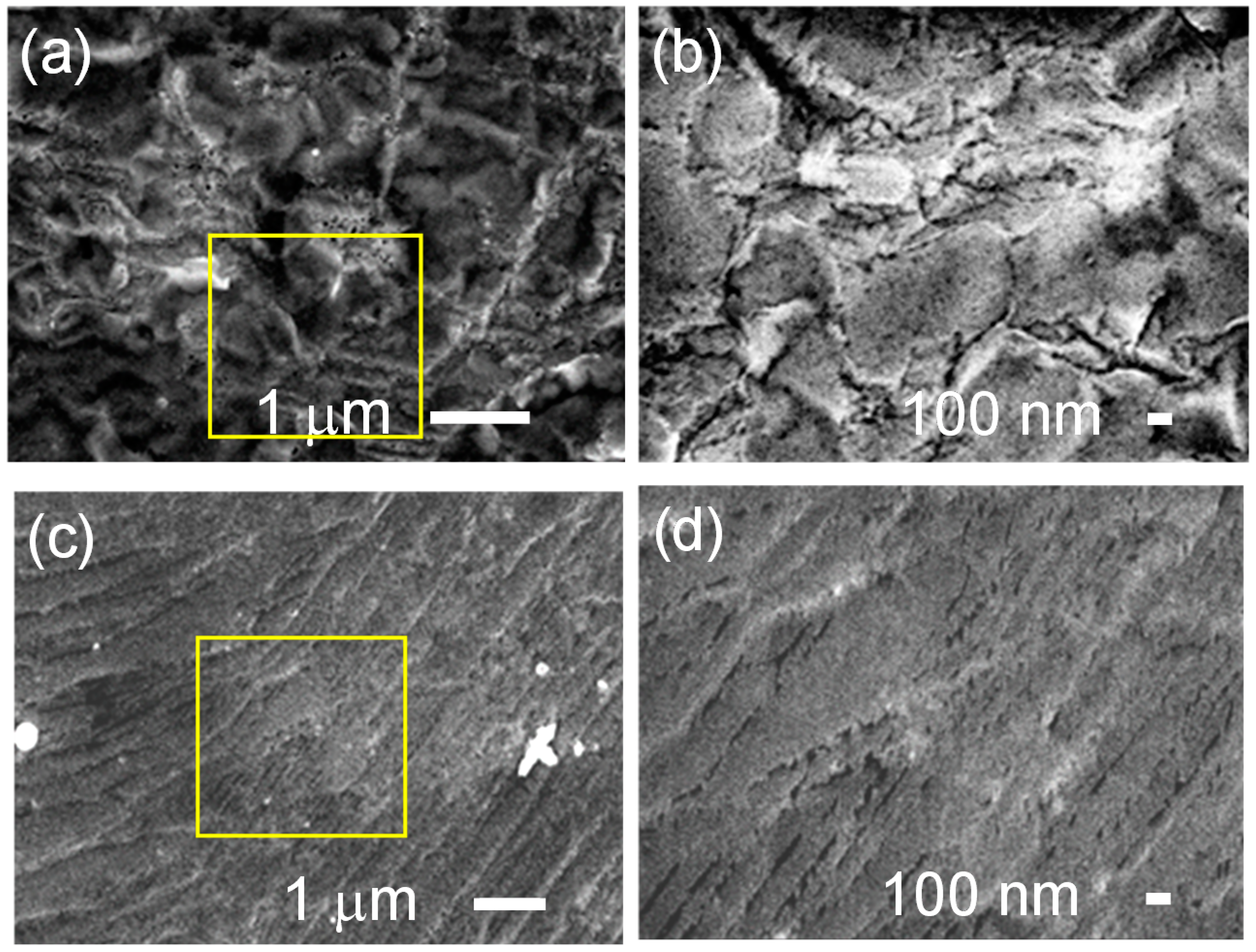
In contrast, the SEM images of 10-nm alumina and 10-nm hafnia on graphene-coated Cu foils in Figure 2, reveal some pinholes, which are more prevalent in alumina films than in hafnia films. The less uniform oxide layer on the graphene can be attributed to the difficulty of nucleation on the chemically inert graphene surface and lack of dangling bonds. Although we employed a two-step ALD deposition process and took advantage of the ability of the metal substrate to change the graphene surface energy, enabling a more efficient trapping of water molecules, there may be a preferred growth of the oxide on the edges of the multilayered graphene sheets. More likely, the oxide deposition process could be further improved.
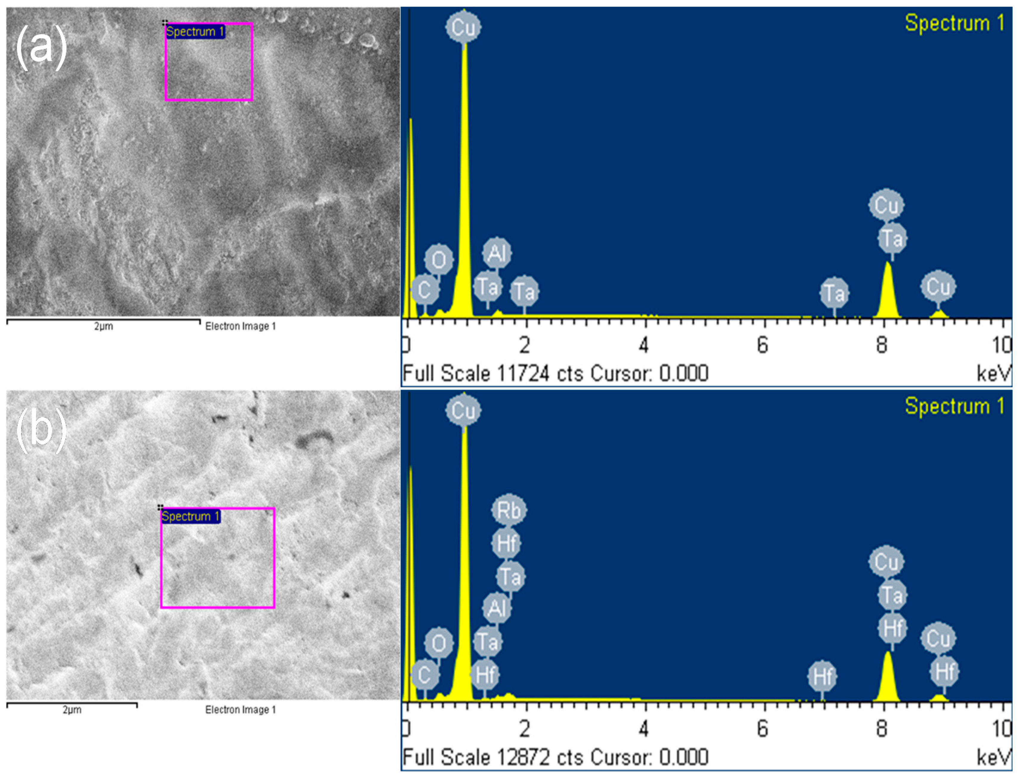
Elemental study via energy dispersive X-ray spectroscopy (EDS) for alumina films, as well as hafnia films, both deposited on graphene/Cu foil, are presented in Figure 3. Besides the strong Cu peaks, small peaks for O, Al and Hf are present in the corresponding EDS spectra, indicating oxide growth on the graphene. The small amount of aluminum in hafnia films may be attributed to sample handling and/or cross-contamination in the ALD system.
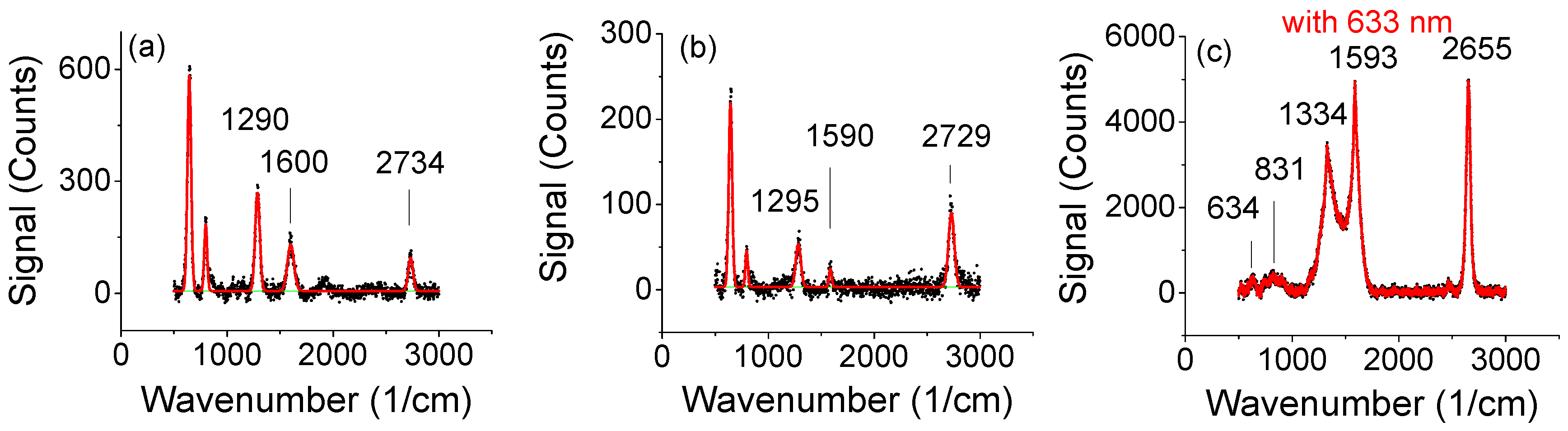
Raman spectra of 10-nm alumina/graphene and 10-nm hafnia/graphene, both on 25-micron Cu foil by using the 442 nm HeCd laser line are shown in Figure 4a,b. Both films seem to exhibit minimal strain while on the copper foil. The two lines below 1000 1/cm belong to the Cu foil itself—these lines have been confirmed by performing Raman experiments on copper-only films (not shown here). There are two features in the Raman data that are worth noting: (1) The CVD grown graphene exhibit one and mostly two layers. This is revealed by the intensity ratio between the 2D (ca. 2700 1/cm) and the G line (ca. 1600 1/cm), as well as by the position of their respective peaks. (2) The disorder line does not appear at ca 1350 1/cm as typically observed with 633 nm HeNe laser (Figure 4c), but at lower frequency (1290 1/cm) (see also Reference [24]). As we shall see later, the transfer films exhibit a shifted disorder line to the higher frequencies. Since the G line has barely shifted, the system calibration should not be in question here. Thus, the type of the disorder [25] might have changed during the film transfer. Finally, we do not observe a line at 2950 1/cm at this point.
3. Transferred Films
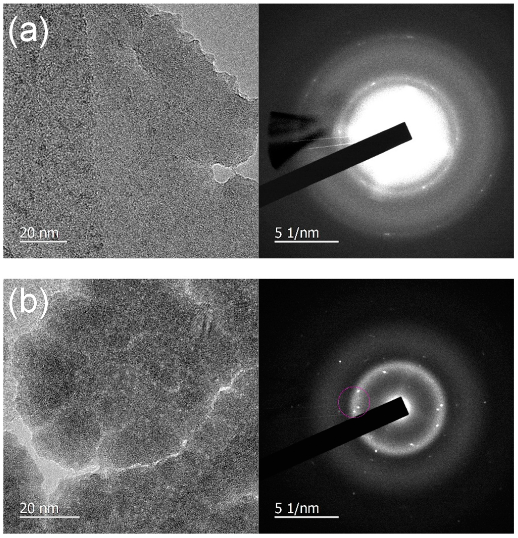
Selected area electron diffraction (SAED) images of the oxide-graphene films transferred onto a TEM grid exhibit crystalline features as well as diffuse circles (Figure 5). The diffuse circles are characteristic to amorphous films and can be attributed to the alumina and hafnia, respectively. It is well known that aluminum oxide and hafnium oxide films grown below 500 °C by ALD are amorphous regardless of the type of substrate [26]. The spotted pattern is given by the graphene layer and reveals multilayered graphene. Multiple hexagonal patterns of different intensity and spot size on the same circle confirm the relative orientation of the graphene layers. The variation in intensity and spot size of the hexagonal rings within the same circle arises due to the variation in inclination of the graphene layers to the beam axis.
Figure 5 also exhibits oxide nucleation and the formation of domains. The nucleation may be explained by a two-component process [27,28] and start at the nucleation site on the graphene.
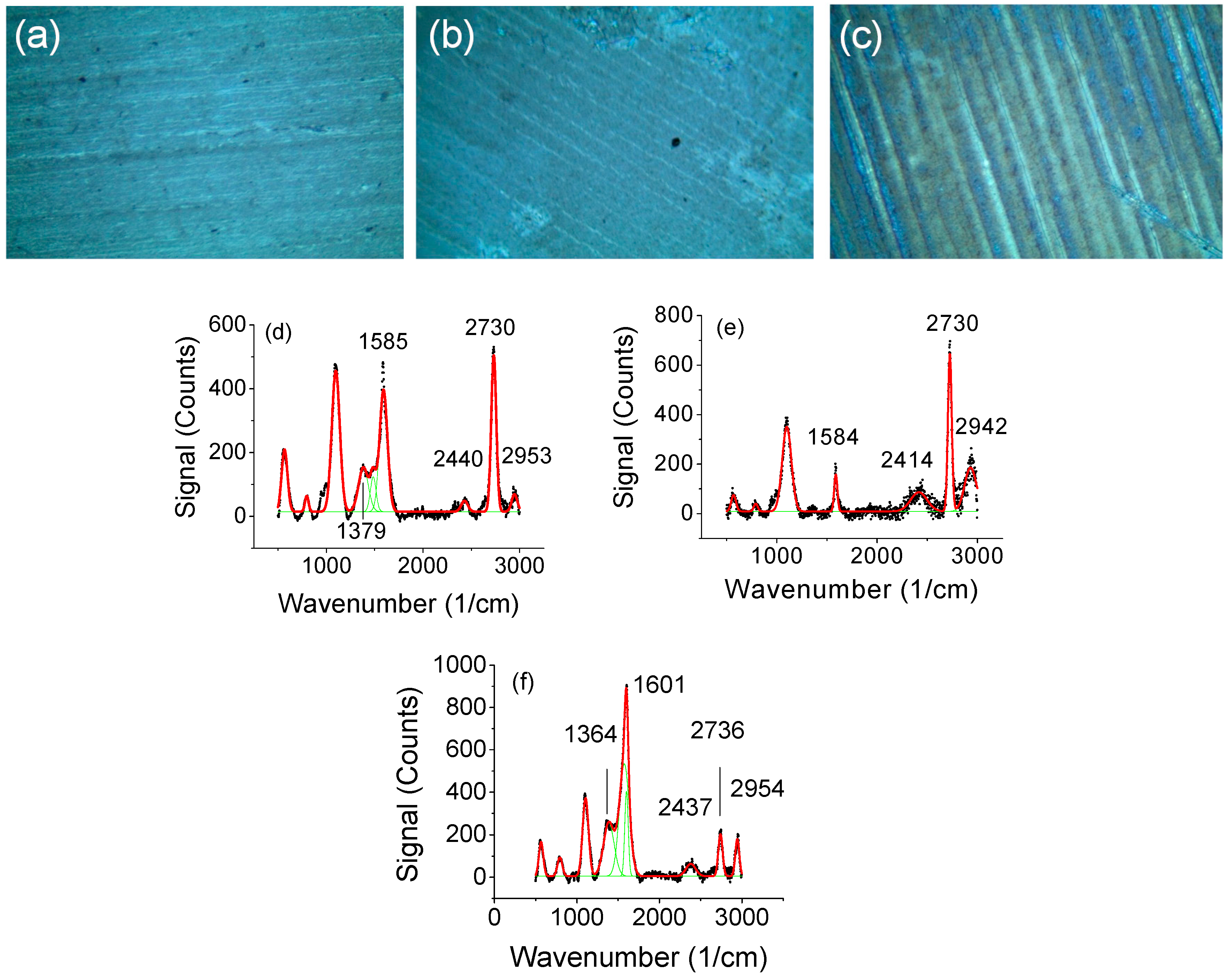
Next, we separate the discussion into oxide-graphene transfer to glassy substrates: (a) without and (b) with an additional step of a 50 nm PMMA layer. In Figure 6a,b, we show optical images of transferred, oxide-graphene films without resorting to an additional PMMA layer, a process which we refer to as a direct transfer. The related Raman spectra are respectively shown in Figure 6d,e. These are transferred films of Figure 5. The 442 nm laser line of a HeCd laser was used to eliminate the signal from the glass slides as much as possible. On one hand, the shorter wavelength has a shorter penetration depth; on the other hand, its energy is larger than, say, the wavelength of a green laser and may lead to undesired excitation related effects.
As clearly visible from Figure 6d, the directly transferred alumina-graphene film gave rise to the G and 2D graphene lines, plus additional ones, most notably at 1389 1/cm and 2950 1/cm. The first may be attributed to a shifted graphitic defect line after the transfer process—we did not see it on the copper foil. Clustering of graphene [25] could lead to such effects since the defects may be modified by either the substrate or the coating. The directly transferred hafnia-graphene film (Figure 6e) exhibits the 2950 1/cm line, as well.
The apparent line at 1478 1/cm for only alumina coated graphene is unusual. It is missing from most known Raman data on graphene and it is even missing from nitrogen-doped graphene layers [29]. It could be a real line, or the result of a large broadening of the D-line at ca 1350 1/cm. The effect must have been introduced during the transfer process since Figure 4 is absent of it. The 1478 1/cm is typical of PMMA [30], which could also be corroborated by the 2950 1/cm line. The issues with this explanation are these: (a) There was no PMMA involved in the transfer process shown in Figure 6d,e and yet the 1478 1/cm line appears only for the alumina coated samples (Figure 6d,f) but not for hafnia coated graphene (Figure 6e). (b) The 2950 1/cm appears in all samples regardless of using PMMA in the transfer process. (c) While not shown here, CVD grown graphene, transferred by only PMMA, lacks the 1478 and the 2950 1/cm lines altogether when measured with either 633 nm or 532 nm lasers. (d) In Figure 6d,f the region between 1300–1650 1/cm is well fitted with three peaks.
The 1478 1/cm is also a line of aromatic rings which could be formed around the OH− defect point in the graphene with the nitrogen in the alumina and adsorbed water molecules during the transfer stage. Strain at the defect point could distort the graphene π-bonds and led to an enhanced reactivity (in this case water) at relatively low temperatures [31,32]. The defect line remained small in the hafnia-graphene layer without any additional line within the range of 1450–1500 1/cm (Figure 6e).
We choose the simpler explanation: The apparent line at 1478 1/cm results from a large D-line broadening. While the region between 1300–1650 1/cm Figure 6d,f may be well-fitted with three peaks, only Figure 6d could be fitted with a specific peak at 1478 1/cm. The origin of the line at ca 2950 1/cm in all samples when using the 442 nm laser is unknown at this point. As we shall see later the line is not observed with a 532 nm laser for oxide-graphene film which was deposited on SiO2 with the aid of PMMA (The PMMA layer was later removed by acetone at 40 °C).
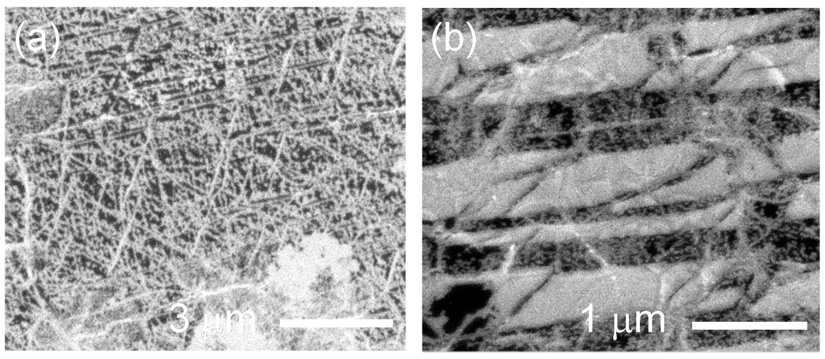
In Figure 7 we show the SEM picture of 5-nm alumina on graphene while on the copper foil. Wires or bands of alumina on graphene showing various growth modes (Figure 7a vs. Figure 7b). As we saw in Figure 5, the alumina-graphene film is formed through nucleation whose domains could be defined by the Cu template. The thinner film is less uniform and its morphology is dictated by the non-uniform dispersion of the nucleation sites on the graphene itself. When the oxide thickness is increased, the domains coalesce, resulting in a more uniform coverage (as exhibited by the 10 nm film in Figure 2).
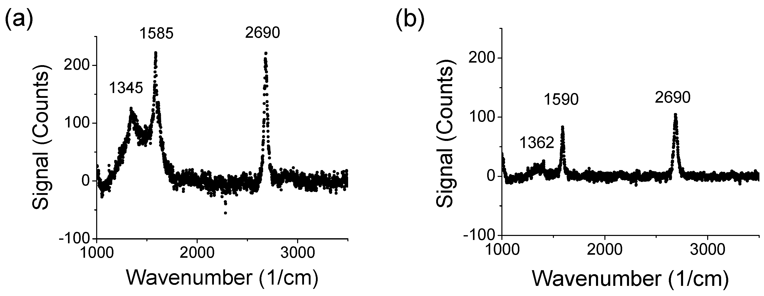
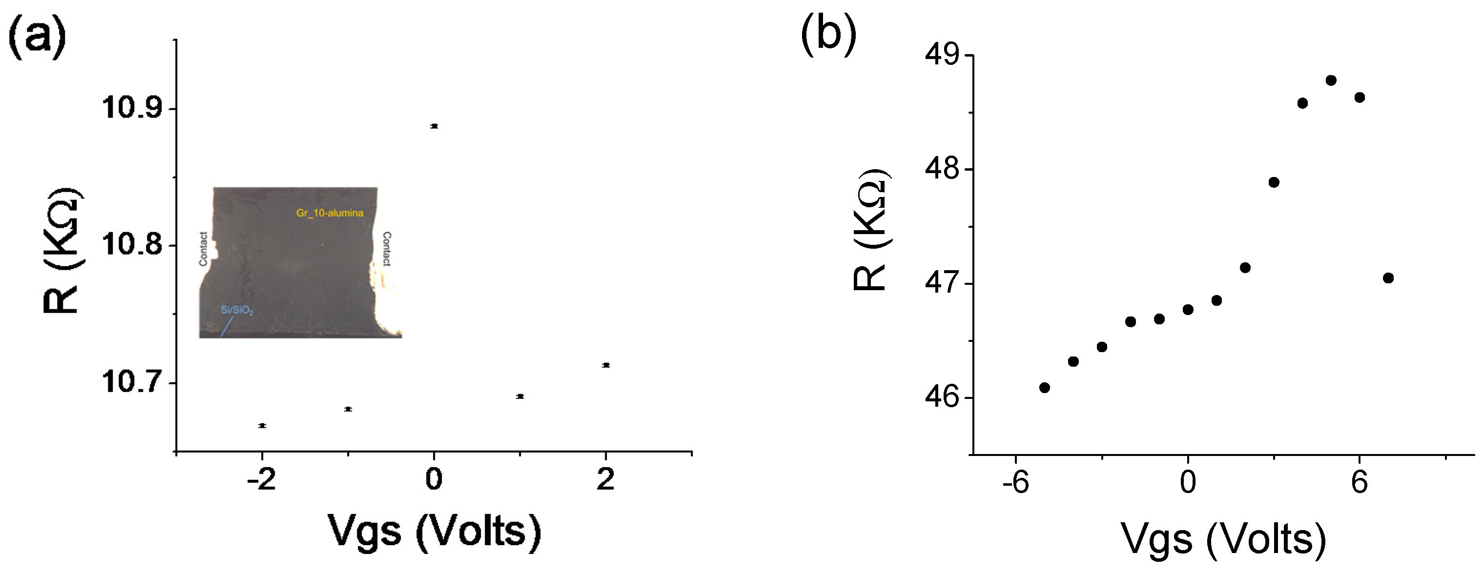
Comparative Raman spectroscopy on a transferred graphene is shown in Figure 8. The films were transferred onto thermally prepared 50-nm SiO2 on a Si wafer. Shown are two samples: One is deposited with 10-nm (Figure 8a) and the other with 5-nm of alumina (Figure 8b). The transfer process involved the use of 50-nm coating of PMMA as described above. The Raman data were taken with a 532 nm laser. Firstly, we note that the samples lack both the 2950 1/cm line and the apparent 1478 1/cm line, exhibited when measured with the 442 nm HeCd laser. Overall, the data suggest a bi-layer graphene. This is based on the positions and the intensity ratio of the G- and 2D-lines of the original films and the data presented in Figure 8. The 2D lines do not exhibit an overall graphene strain. Secondly, the thicker oxide exhibits an increase in both intensity and width of the D line with respect to the G-line as shown in Figure 8a. These allude to local strained defects, as the thickness of the oxide has increased. The small up-shift of the G-line in Figure 8b with respect to Figure 8a could be explained by unintentional surface charges added in the transfer stage for the 5-nm oxide on graphene (Figure 8b)—small surface potential tends to increase the graphene doping, thereby up-shifting the G-line without altering the intensity of the 2D line [33]. The electrical data of Figure 9 corroborate such behavior; the thicker oxide film on graphene has a G-line at 1585 1/cm with its Dirac point at Vg = 0 V (Figure 9a) whereas the thinner 5-nm oxide layer on graphene exhibits a shifted G-line towards 1590 1/cm and its Dirac point exhibited at Vg = 5 V.
For the electrical conductance we used conductive epoxy to define the source and drain (S-D) electrodes. A double adhesive copper tape was used to connect to the Si wafer that served as a back gate electrode. In Figure 9a the S-D electrodes were deposited on the top alumina layer whereas in Figure 9b, the electrodes were first deposited on the 50-nm SiO2 before the oxide-graphene film was transferred. The first technique takes advantage of the pinholes in the alumina layer. The second technique may have exposed the epoxy (and the entire surface) to additional surface charges while suspending in water. Extra surface charge results in a shift of the Dirac point as seen in Figure 9b. The increase in contact resistance for the 5-nm alumina on graphene may also imply that the epoxy suffered extra oxidation (and thereby extra resistance) while in the water, albeit without affecting its ohmic characteristics.
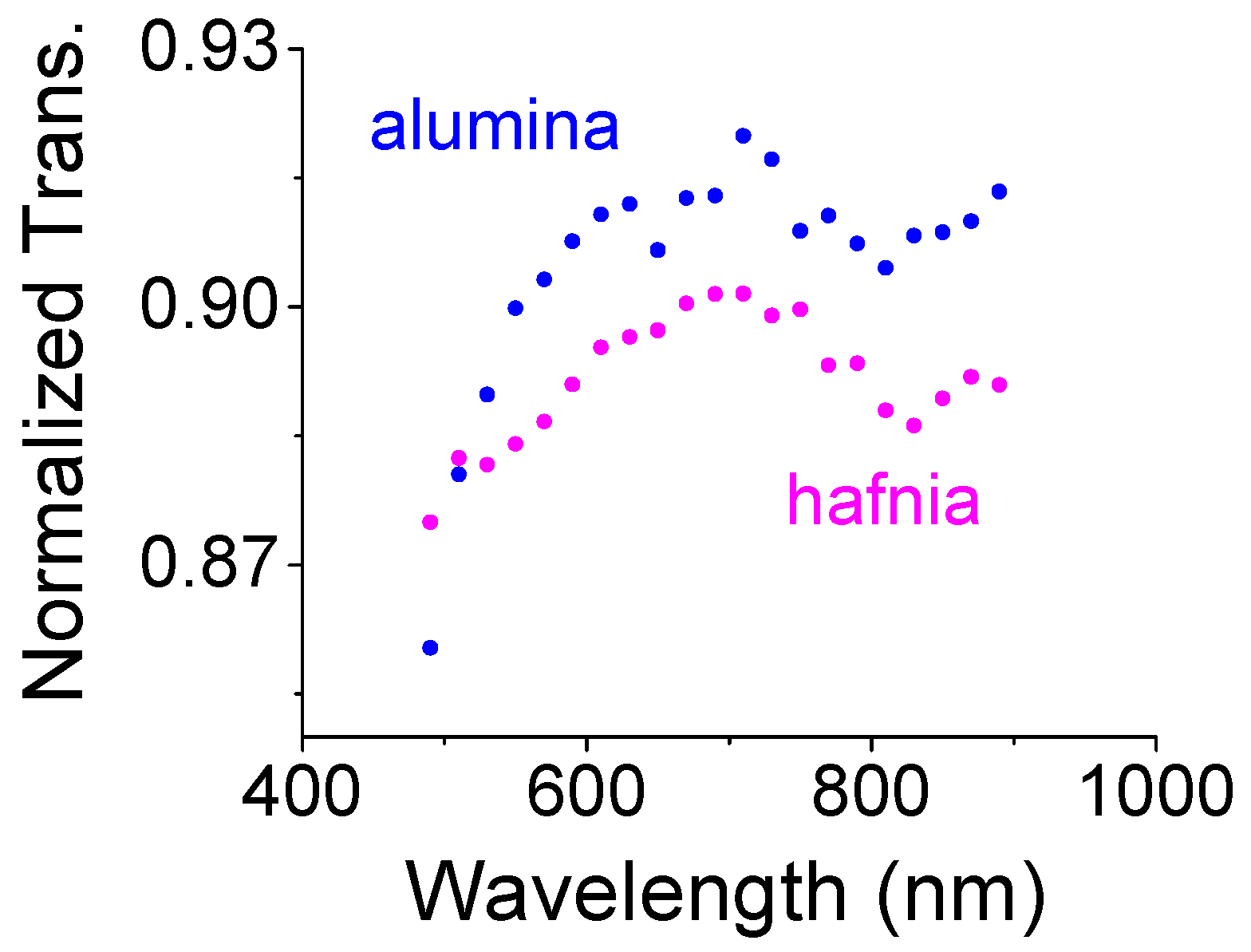
Optical transmissions for transferred oxide-graphene films are presented in Figure 10. All the transferred films were deposited on glass slides. The data were normalized by the transmission of only graphene on the glass. The samples were tilted a bit to minimize multi-reflection paths within the glass due to the relatively large refractive index of the oxide compared to the glass itself. The 10-nm alumina-graphene on a glass slide appeared darker to the naked eye; this may be due to scattering from the less homogeneous alumina film. Nevertheless, its optical transmission is larger than for hafnia.
4. Conclusions
A comprehensive study of transferred graphene films thin protective oxides revealed that the oxide layer did not contribute to a major overall film strain. The alumina on graphene exhibited more pin-holes than hafnia on graphene. Raman data pointed to a broaden defect D-line in alumina-graphene films but none in hafnia-graphene. Coating the oxide-graphene layer with an additional 50 nm of PMMA made the transfer of graphene easy and its removal very efficient.
Author Contributions
H.G. conceived, designed and performed the experiments with assistance from L.S., A.V.S. and Y.L.; L.S. and A.V.S. contributed oxide and graphene fabrication tools, respectively; Y.L. contributed TEM analysis tool; D.G., L.O. and B.F. contributed optical and electronic analysis tools; H.G. analyzed the data with assistance from L.S. and Y.L.; H.G. wrote the paper with assistance from L.S., A.V.S. and B.F. All authors contributed to discussions and the production of the manuscript.
Funding
This research received partial support from U.S. Department of Energy, Office of Science, under Contract No. DE-AC02-06CH11357.
Acknowledgments
This work was performed, in part, at the Center for Nanoscale Materials, a U.S. Department of Energy Office of Science User Facility. We thank X. Miao of NJIT for help with the EDS pictures and a Raman scan.
Conflicts of Interest
The authors declare no conflicts of interest.
References
- Suk, J.W.; Kitt, A.; Magnuson, C.W.; Hao, Y.; Ahmed, S.; An, J.; Swan, A.K.; Goldberg, B.B.; Ruoff, R.S. Transfer of CVD-Grown Monolayer Graphene onto Arbitrary Substrates. ACS Nano 2011, 5, 6916–6924. [Google Scholar] [CrossRef] [PubMed]
- Lee, Y.; Bae, S.; Jang, H.; Jang, S.; Zhu, S.-E.; Sim, S.H.; Song, Y.I.; Hong, B.H.; Ahn, J.-H. Wafer-scale synthesis and transfer of graphene films. Nano Lett. 2010, 10, 490–493. [Google Scholar] [CrossRef] [PubMed]
- Gao, L.; Ren, W.; Xu, H.; Jin, L.; Wang, Z.; Ma, T.; Ma, L.; Zhang, Z.; Fu, Q.; Peng, L.; et al. Repeated growth and bubbling transfer of graphene with millimetre-size single-crystal grains using platinum. Nat. Commun. 2012, 3, 699. [Google Scholar] [CrossRef] [PubMed] [Green Version]
- Lee, J.; Kim, Y.; Shin, H.-J.; Lee, C.; Lee, D.; Moon, C.-Y.; Lim, J.; Jun, S.C. Clean transfer of graphene and its effect on contact resistance. Appl. Phys. Lett. 2013, 103, 103104. [Google Scholar] [CrossRef]
- Ko, P.J.; Takahashi, H.; Koide, S.; Sakai, H.; Thu, T.V.; Okada, H.; Sandhu, A. Simple method to transfer graphene from metallic catalytic substrates to flexible surfaces without chemical etching. J. Phys. Conf. Ser. 2013, 433, 012002. [Google Scholar] [CrossRef] [Green Version]
- Boscá, A.; Pedrós, J.; Martínez, J.; Palacios, T.; Calle, F. Automatic graphene transfer system for improved material quality and efficiency. Sci. Rep. 2016, 6, 21676. [Google Scholar] [CrossRef] [PubMed]
- Chen, Y.; Gong, X.; Gai, J. Progress and Challenges in Transfer of Large-Area Graphene. Films Adv. Sci. 2016, 3, 1500343. [Google Scholar] [CrossRef]
- Wang, M.C.; Moestopo, W.P.; Takekuma, S.; Barna, S.F.; Haasch, R.T.; Nam, S. A sustainable approach to large area transfer of graphene and recycling of the copper substrate. J. Mater. Chem. C 2017, 5, 11226–11232. [Google Scholar] [CrossRef]
- van Ngoc, H.; Qian, Y.; Han, S.K.; Kang, D.J. PMMA-Etching-Free Transfer of Wafer-scale Chemical Vapor Deposition Two-dimensional Atomic Crystal by a Water Soluble Polyvinyl Alcohol Polymer Method. Sci. Rep. 2016, 6, 33096. [Google Scholar] [CrossRef] [Green Version]
- Meric, I.; Han, M.Y.; Young, A.F.; Özyilmaz, B.; Kim, P.; Shepard, K.L. Current Saturation in Zero-Bandgap, Top-Gated Graphene Field-Effect Transistors. Nat. Nanotechnol. 2008, 3, 654–659. [Google Scholar] [CrossRef]
- Zou, K.; Hong, X.; Keefer, D.; Zhu, J. Deposition of High-Quality HfO2 on Graphene and the Effect of Remote Oxide Phonon Scattering. Phys. Rev. Lett. 2010, 105, 126601. [Google Scholar] [CrossRef] [PubMed]
- Alles, H.; Aarik, J.; Aidla, A.; Fay, A.; Kozlova, J.; Niilisk, A.; Pärs, M.; Rähn, M.; Wiesner, M.; Hakonen, P.; Sammelselg, V. Atomic Layer Deposition of HfO2 on Graphene from HfCl4 and H2O. Cent. Eur. J. Phys. 2011, 9, 319–324. [Google Scholar] [CrossRef]
- Moon, J.S.; Curtis, D.; Hu, M.; Wong, D.; McGuire, C.; Campbell, P.M.; Jernigan, G.; Tedesco, J.L.; VanMil, B.; Myers-Ward, R.; et al. Epitaxial Graphene RF Field-Effect Transistors on Si-Face 6H-SiC Substrates. IEEE Electron Dev. Lett. 2009, 30, 650–652. [Google Scholar] [CrossRef]
- Kim, S.; Nah, J.; Jo, I.; Shahrjerdi, D.; Colombo, L.; Yao, Z.; Tutuc, E.; Banerjee, S.K. Realization of a High Mobility Dual-Gated Graphene Field-Effect Transistor with Al2O3 Dielectric. Appl. Phys. Lett. 2009, 94, 062107. [Google Scholar] [CrossRef]
- Wang, X.; Tabakman, S.M.; Dai, H. Atomic Layer Deposition of Metal Oxides on Pristine and Functionalized Graphene. J. Am. Chem. Soc. 2008, 130, 8152–8153. [Google Scholar] [CrossRef] [PubMed] [Green Version]
- Farmer, D.B.; Chiu, H.-Y.; Lin, Y.-M.; Jenkins, K.A.; Xia, F.; Avouris, P. Utilization of a Buffered Dielectric to Achieve High Field-Effect Carrier Mobility in Graphene Transistors. Nano Lett. 2009, 9, 4474–4478. [Google Scholar] [CrossRef] [PubMed] [Green Version]
- Lee, B.; Park, S.-Y.; Kim, H.-C.; Cho, K.J.; Vogel, E.M.; Kim, M.J.; Wallace, R.M.; Kim, J. Conformal Al2O3 Dielectric Layer Deposited by Atomic Layer Deposition for Graphene-Based Nanoelectronics. Appl. Phys. Lett. 2008, 92, 203102. [Google Scholar] [CrossRef]
- Lee, B.; Mordi, G.; Kim, M.J.; Chabal, Y.J.; Vogel, R.M.; Wallace, R.M.; Cho, K.J.; Colombo, L.; Kim, J. Characteristics of High-k Al2O3 Dielectric Using Ozone-Based Atomic Layer Deposition for Dual-Gated Graphene Devices. Appl. Phys. Lett. 2010, 97, 043107. [Google Scholar] [CrossRef]
- Zheng, L.; Cheng, X.; Cao, D.; Wang, G.; Wang, Z.; Xu, D.; Xia, C.; Shen, L.; Yu, Y.; Shen, D. Improvement of Al2O3Films on Graphene Grown by Atomic Layer Deposition with Pre-H2O Treatment. ACS Appl. Mater. Interfaces 2014, 6, 7014–7019. [Google Scholar] [CrossRef] [PubMed]
- Cabrero-Vilatela, A.; Alexander-Webber, J.A.; Sagade, A.A.; Aria, A.I.; Braeuninger-Weimer, P.; Martin, M.; Weatherup, R.S.; Hofmann, S. Atomic layer deposited oxide films as protective interface layers for integrated graphene transfer. Nanotechnology 2017, 28, 485201. [Google Scholar] [CrossRef] [PubMed] [Green Version]
- Dlubak, B.; Kidambi, P.R.; Weatherup, R.S.; Hofmann, S.; Robertson, J. Substrate-assisted nucleation of ultra-thin dielectric layers on graphene by atomic layer deposition. Appl. Phys. Lett. 2012, 100, 173113. [Google Scholar] [CrossRef] [Green Version]
- Gulotty, R.; Das, S.; Liu, Y.; Sumant, A.V. Effect of hydrogen flow during cooling phase to achieve uniform and repeatable growth of bilayer graphene on copper foils over large area. Carbon 2014, 77, 341–350. [Google Scholar] [CrossRef]
- Groner, M.D.; Elam, J.W.; Fabreguette, F.H.; George, S.M. Electrical characterization of thin Al2O3 films grown by atomic layer deposition on silicon and various metal substrates. Thin Solid Films 2012, 413, 186–197. [Google Scholar] [CrossRef]
- Marta, B.; Leordean, C.; Istvan, T.; Botiz, I.; Astilean, S. Efficient etching-free transfer of high quality, large-area CVD grown graphene onto polyvinyl alcohol films. Appl. Surf. Sci. 2016, 363, 613–618. [Google Scholar] [CrossRef]
- Ferrari, A.C.; Solid State Communications. Raman spectroscopy of graphene and graphite: Disorder, electron–phonon coupling, doping and nonadiabatic effects. Solid State Commun. 2007, 143, 47–57. [Google Scholar] [CrossRef]
- Miikkulainen, V.; Leskelä, M.; Ritala, M.; Puurunen, R.L. Crystallinity of inorganic films grown by atomic layer deposition: Overview and general trends. J. Appl. Phys. 2013, 113, 101. [Google Scholar] [CrossRef]
- Määttänen, A.; Vehkamäki, H.; Lauri, A.; Napari, I.; Kulmala, M. Two-component heterogeneous nucleation kinetics and an application to Mars. J. Chem. Phys. 2007, 127, 134710. [Google Scholar] [CrossRef] [PubMed]
- Stauffer, D. Kinetic theory of two-component (“hetero-molecular”) nucleation and condensation. J. Aerosol Sci. 1976, 7, 319–333. [Google Scholar] [CrossRef]
- Lv, R.; Li, Q.; Botello-Mendez, A.R.; Hayashi, T.; Wang, B.; Berkdemir, A.; Hao, Q.; Elıas, A.L.; Cruz-Silva, R.; Gutierrez, H.R.; et al. Nitrogen-doped graphene: Beyond single substitution and enhanced molecular sensing. Sci. Rep. 2012, 2, 586. [Google Scholar] [CrossRef]
- Li, Z.; Kinloch, I.A.; Young, R.J. The role of interlayer adhesion in graphene oxide upon its reinforcement of nanocomposites. Philos. Trans. R. Soc. A 2015, 374. [Google Scholar] [CrossRef]
- Banhart, F.; Kotakoski, J.; Krasheninnikov, A.V. Structural Defects in Graphene. ACS Nano 2011, 5, 26–41. [Google Scholar] [CrossRef] [PubMed]
- Robinson, J.T.; Zalalutdinov, M.K.; Cress, C.D.; Culbertson, J.C.; Friedman, A.L.; Merrill, A.; Landi, B.J. Graphene Strained by Defects. ACS Nano 2017, 11, 4745–4752. [Google Scholar] [CrossRef] [PubMed]
- Das, A.; Isana, S.P.; Chakraborty, B.; Piscanec, S.; Saha, S.K.; Waghmare, U.V.; Novoselov, K.S.; Krishnamurthy, H.R.; Geim, A.K.; Ferrari, A.C.; et al. Monitoring dopants by Raman scattering in an electrochemically top-gated graphene transistor. Nat. Nano 2008, 3, 210–215. [Google Scholar] [CrossRef] [PubMed] [Green Version]
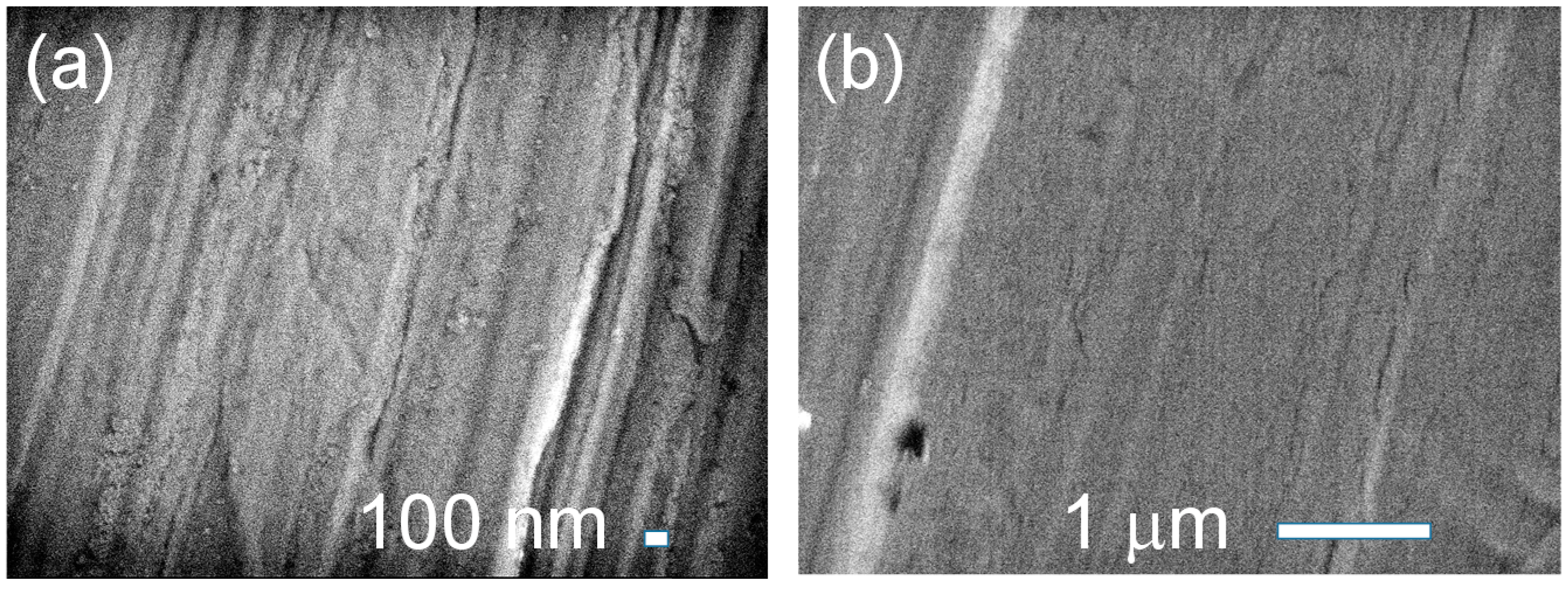
Figure 1.
SEM images of 10-nm thick alumina (a) and 10-nm thick hafnia (b) on bare 25 micron thick Cu foil illustrating a fairly uniform coverage of the oxide on the copper.
Figure 1.
SEM images of 10-nm thick alumina (a) and 10-nm thick hafnia (b) on bare 25 micron thick Cu foil illustrating a fairly uniform coverage of the oxide on the copper.

Figure 2.
SEM images of 10-nm thick alumina (a,b) and 10-nm thick hafnia (c,d) on graphene coated 25 microns thick Cu foil. The yellow marked area in (a,c) is magnified in (b,d).
Figure 2.
SEM images of 10-nm thick alumina (a,b) and 10-nm thick hafnia (c,d) on graphene coated 25 microns thick Cu foil. The yellow marked area in (a,c) is magnified in (b,d).

Figure 3.
EDS of (a) alumina film and (b) hafnia film grown on graphene/copper foil.

Figure 4.
(a) 10-nm alumina-graphene on a 25 micron Cu foil. (b) 10-nm hafnia-graphene on 25 micron Cu foil. The two lines below 1000 1/cm belong to the Cu foil itself. The 1290 1/cm is the defect D line when exposed to the 442 nm laser line. Local stresses and differences between two- and one-layer graphene may have contributed to the graphene’s line shifts towards the higher frequencies in (a) vs (b). (c) Same sample as (a); 10-nm alumina-graphene on a 25 micron Cu foil measured with 633 nm HeNe laser. The time exposures in (c) was longer and the intensity was larger than for (a,b).

Figure 5.
TEM image and diffraction pattern of (a) 10-nm thick alumina-graphene film and (b) 10-nm hafnia-graphene film suspended on a TEM grid.
Figure 5.
TEM image and diffraction pattern of (a) 10-nm thick alumina-graphene film and (b) 10-nm hafnia-graphene film suspended on a TEM grid.

Figure 6.
(a) 10-nm alumina-graphene on glass. (b) 10-nm hafnia-graphene on glass. (c) 10-nm alumina-graphene on glass transferred with an additional 50-nm thick PMMA layer. The microscope objective was x20. Raman spectra taken with 442 nm HeCd laser: (d) 10-nm thick alumina-graphene. (e) 10-nm thick hafnia-graphene. (f) 10-nm alumina graphene with an additional PMMA layer. In (d) and (f), the region between 1300-1650 1/cm is well-fitted with three peaks rather the expected two. The lines at 1100 1/cm and below are attributed to the glass slide (corroborated separately but not shown here).

Figure 7.
(a,b) Various growth modes can be identified for 5-nm alumina on graphene when still on a 25 micron thick Cu foil.
Figure 7.
(a,b) Various growth modes can be identified for 5-nm alumina on graphene when still on a 25 micron thick Cu foil.

Figure 8.
Comparative Raman spectra of bilayer graphene deposited with alumina when transferred onto thermally prepared 50-nm SiO2/Si. (a) 10-nm alumina on transferred graphene. (b) 5-nm alumina on a transferred graphene. Raman data were obtained with a 532 nm laser.
Figure 8.
Comparative Raman spectra of bilayer graphene deposited with alumina when transferred onto thermally prepared 50-nm SiO2/Si. (a) 10-nm alumina on transferred graphene. (b) 5-nm alumina on a transferred graphene. Raman data were obtained with a 532 nm laser.

Figure 9.
Electrical data for (a) 10-nm alumina on graphene and (b) 5-nm alumina on graphene. Shown is film resistance as a function of gate voltage. Both films were transferred onto 50-nm thick SiO2 on a Si wafer. Both curves were obtained in up and down directions.
Figure 9.
Electrical data for (a) 10-nm alumina on graphene and (b) 5-nm alumina on graphene. Shown is film resistance as a function of gate voltage. Both films were transferred onto 50-nm thick SiO2 on a Si wafer. Both curves were obtained in up and down directions.

Figure 10.
Transmission through 10-nm thick oxide on graphene when transferred to a glass slide. The data were normalized by the transmission of only graphene film on a glass slide.
Figure 10.
Transmission through 10-nm thick oxide on graphene when transferred to a glass slide. The data were normalized by the transmission of only graphene film on a glass slide.

© 2018 by the authors. Licensee MDPI, Basel, Switzerland. This article is an open access article distributed under the terms and conditions of the Creative Commons Attribution (CC BY) license (http://creativecommons.org/licenses/by/4.0/).
Share and Cite
MDPI and ACS Style
Grebel, H.; Stan, L.; Sumant, A.V.; Liu, Y.; Gosztola, D.; Ocola, L.; Fisher, B. Transfer of Graphene with Protective Oxide Layers. ChemEngineering 2018, 2, 58. https://0-doi-org.brum.beds.ac.uk/10.3390/chemengineering2040058
AMA Style
Grebel H, Stan L, Sumant AV, Liu Y, Gosztola D, Ocola L, Fisher B. Transfer of Graphene with Protective Oxide Layers. ChemEngineering. 2018; 2(4):58. https://0-doi-org.brum.beds.ac.uk/10.3390/chemengineering2040058
Chicago/Turabian StyleGrebel, Haim, Liliana Stan, Anirudha V. Sumant, Yuzi Liu, David Gosztola, Leonidas Ocola, and Brandon Fisher. 2018. "Transfer of Graphene with Protective Oxide Layers" ChemEngineering 2, no. 4: 58. https://0-doi-org.brum.beds.ac.uk/10.3390/chemengineering2040058