
Recent Development of Optofluidics for Imaging and Sensing Applications


1
Institute of Environmental Engineering, ETH Zürich, 8093 Zürich, Switzerland
2
Laboratory for Advanced Analytical Technologies, Empa, Swiss Federal Laboratories for Materials Science and Technology, 8600 Dübendorf, Switzerland
*
Authors to whom correspondence should be addressed.
Chemosensors 2022, 10(1), 15; https://0-doi-org.brum.beds.ac.uk/10.3390/chemosensors10010015
Submission received: 31 October 2021
/
Revised: 25 December 2021
/
Accepted: 30 December 2021
/
Published: 1 January 2022
(This article belongs to the Special Issue Nanophotonic Biosensors: Challenges and Development)
Abstract
:Optofluidics represents the interaction of light and fluids on a chip that integrates microfluidics and optics, which provides a promising optical platform for manipulating and analyzing fluid samples. Recent years have witnessed a substantial growth in optofluidic devices, including the integration of optical and fluidic control units, the incorporation of diverse photonic nanostructures, and new applications. All these advancements have enabled the implementation of optofluidics with improved performance. In this review, the recent advances of fabrication techniques and cutting-edge applications of optofluidic devices are presented, with a special focus on the developments of imaging and sensing. Specifically, the optofluidic based imaging techniques and applications are summarized, including the high-throughput cytometry, biochemical analysis, and optofluidic nanoparticle manipulation. The optofluidic sensing section is categorized according to the modulation approaches and the transduction mechanisms, represented by absorption, reflection/refraction, scattering, and plasmonics. Perspectives on future developments and promising avenues in the fields of optofluidics are also provided.
1. Introduction
Microfluidics represents a technique of manipulating fluids at a micrometer scale in an integrated and miniaturized platform [1]. As one of the most prominent small-size effects, the viscous force becomes significantly predominant in guiding the micro flow instead of the inertial force, and the Reynolds number (Re) is dramatically low, typically Re << 1 [2,3]. The fluid within microfluidics behaves as a laminar flow, so mixing is diffusion-limited [4,5,6]. Taking advantage of the miniaturized lab-on-a-chip design, the microfluidic device requires a low volume of analyte sample and reagents in biochemical analysis [5]. The excellent capability in analyzing continuous-flow samples is another advantage of the microfluidic device compared to conventional quantitative chemical analysis approaches, such as the well-based measurement [7]. In addition, rapid thermal transfer between the device and the contained fluid enables microfluidic devices for biochemical reactions under a well-controlled temperature [2]. Noticeably, the microfluidic device has been used as a powerful platform for analyzing micro- and nano-scale targets, e.g., cells [8,9], particles [10], and droplets [11], exhibiting outstanding capabilities in separating, sorting, and characterizing biochemical targets of interest. Despite the mentioned advantages, challenges remain to be resolved, mainly in manufacturing complex 3D fluidic structures, precise fluid processing, achieving multi-functionalities (e.g., fluid manipulation, optical manipulation, and sample detection), and miniaturizing the entire system.
Optical detection is an essential approach for biochemical analysis, which requires optical components such as the monochromatic or polychromatic light sources, waveguide, optical fiber, objective lens, photodetector, and spectrometer. The combination of optics and microfluidics has resulted in the advent of optofluidics, representing a new analytical field based on the interaction of light and fluid [12,13,14,15,16,17]. In recent years, micro-optics have received growing attention, involving the miniaturization of optical components, e.g., lens, reflecting mirror, prism, grating, and waveguide, down to micrometer scale [18]. The integration of miniaturized optics into a microfluidic platform, that is, constructing novel optofluidic systems, has remarkably contributed to the compaction of the entire system and the enhancement of the detection performance (e.g., sensitivity improvement in biochemical analysis, multi-analyte array-based detection and high-throughput flow-based chemical analysis).
The recent development of optofluidic fabrication techniques, the integration of novel optical elements, and the emergence of new applications have resulted in significant progress in the fields of analytical chemistry and biomedical engineering. This progress motivated us to summarize and discuss these novel advances in this review. First, the fabrication techniques for optofluidic devices are introduced in terms of the fabrication strategies, the functionalities of key components, and the characteristics of processing materials. Following this section, we provide a couple of recent research directions regarding optofluidic-based imaging applications. Then, optofluidic-based sensing applications are presented according to the transduction mechanisms, including absorption, refraction, scattering, and plasmonics. Finally, we conclude this review and provide our perspectives on optofluidic developments in the future. It should be noted that although we focus on novel optical elements (e.g., integrated optics) for optofluidic applications, some emerging studies using microfluidic devices and conventional optics are also mentioned; for instance, based on the advantages of microfluidics, novel optical detection functions can be realized even with a traditional optical analysis system.
2. Fabrication Techniques for Optofluidic Devices
In this section, we introduce the typical strategies and techniques for the fabrication of optofluidic devices (e.g., direct manufacture and mold replication), highlight the key integrated components (fluid control units, light manipulation structure, and signal transduction units), and briefly illustrate the commonly used materials for optofluidic devices.
2.1. Fabrication Strategy
2.1.1. Direct Manufacture
3D printing, micromilling, and direct laser writing have been employed for directly fabricating optofluidic channels, chambers, and cavities. Monaghan et al. used a 3D printed chip integrated with optical fibers for UV-Vis spectrum measurement [19], as shown in Figure 1a. The fiber was placed in the pre-aligned U-shape fiber groove for monitoring organic reactions online. As shown in Figure 1a, the printed nuts at the inlet and outlet ensured a connection using tubes without leakage. More examples of 3D printing for fabricating microfluidic chips can be found in earlier review papers [20,21]. Three-dimensional printing features the flexibility of fabricating microfluidic devices with built-in 3D structures at a low cost, despite the possible restrictions of material choices. Micromilling represents another fabrication approach using a subtractive manufacturing strategy. Micromilling works for both plastic and glass and has flexibility in fabricating customized structures [22,23]. For example, Ku et al. employed a commercial micromilling machine to prototype the glass substrate into a Y-shape microfluidic mixer [22], as shown in Figure 1b. The combined parameters of low cutting depth, high spindle speed, and low feed rate improved the surface roughness of fabricated structures. Guckenberger et al. reviewed the application of micromilling for fabricating plastic microfluidic devices. Despite its utility, insufficient resolution may hinder it for fabricating precise structures [23]. Direct laser writing has received rising attention in micro-fabrication. For example, Hu et al. directly used a femtosecond laser to fabricate an optofluidic chip in photosensitive glass, as shown in Figure 1c. The 3D microlens was simultaneously integrated in the chip, representing a high capability of direct laser writing in fabricating complicated structures [24]. However, such a direct fabrication of built-in high-resolution structures requires special photosensitive glass and a long processing time. Generally, despite the flexibility of direct manufacture, it may be difficult to strike a balance between resolution, efficiency, and limitation of material choices when scaling up applications.
2.1.2. Mold Replication
Mold replication has been recommended as a classical approach for prototyping optofluidic devices with excellent reproducibility and efficiency. Usually, molds can be prepared through micromilling [25], 3D printing [26,27], UV lithography [28], and two-photon stereolithography [7]. Despite the possible slow process of fabricating high-resolution structures, the mold can be sustainably used once prototyped. Mold structures can be replicated with a high level of fidelity and efficiency. Lin et al. reported a 3D printed metal mold, from which thermoplastic (poly(methyl methacrylate), PMMA) microfluidic devices were fabricated via hot embossing [27], as shown in Figure 2a. UV lithography is a widely used technique for fabricating molds with planar structures. SU-8 photoresist is often selectively cured as a mold according to the patterned mask. For example, Tang et al. fabricated planar structures for valve control and central supply of reagents using UV lithography [28], as shown in Figure 2b. Subsequently, structures in the mold were replicated by curing PDMS. By combining the thermal reflow process, UV lithography can also be used to fabricate structures with a curved surface [29,30]. The thermal reflow refers to reshaping the original structure into new surface profiles during a heating process [31]. For example, Holzner et al. used thermal reflow to change the pillar array to a microlens array on a glass substrate [30]. Compared to UV lithography, two-photon stereolithography represents a powerful technique to fabricate structures with a resolution down to sub-micrometer level and has excellent capability to fabricate the mold with high-resolution 3D structures [7,28,32,33,34]. For example, Tang et al. employed two-photo stereolithography to fabricate a mold incorporated with a cascaded 3D microlens for sensitivity-adjustable refractive index (RI) sensing [33]. After the PDMS casting, an optofluidic chip was prepared, as shown in Figure 2c. In another research work by Tang and coworkers, they directly used two-photo stereolithography to fabricate the rounded flow channel and the 3D spherical microlens, eliminating the thermal reflow required in UV lithography [28]. According to the importance of the different structures, two-photon stereolithography can be flexibly implemented with a hierarchical printing strategy by selecting appropriate parameters [28] or combining with UV lithography [35].
We provide a concise summary of a number of the aforementioned fabrication techniques in Table 1, in which their applications, advantages, and disadvantages are presented for a clear comparison.
2.2. Key Optofluidic Components
Key components, including micro-valves, hydraulic structures, optical fibers, microlenses, micro-mirrors, waveguides, and functional photonic nanostructures can be integrated in optofluidic chips for specific purposes. This section introduces these key optofluidic components based on their functionalities, i.e., the fluid control, light manipulation, and signal transduction.
2.2.1. Fluid Control
The incorporation of micro-valves represents substantial progress in the development of optofluidic or microfluidic chips [36,37]. The micro-valve usually consists of a control layer and a flow channel with a curved cross section. Through pneumatically controlling the thin elastic membrane of the control layer, the flow in a channel can be opened or closed in a programmable manner. Micro-valves have been employed in a number of application fields, e.g., droplet combination and dilution [38,39], optical switches [28], and cell analysis [40]. Hydraulic structures have also been configured in optofluidic chips for flow control. Simultaneously pumping sheath flows can confine the sample flow at the center of the microchannel for particle or cell detection [41]. The manipulation of fluid by a special hydraulic structure can also function as a waveguide. For example, Yang et al. presented a Dean flow by centrifugal effects in a curved channel for optofluidic dye lasers [42].
2.2.2. Light Manipulation
Optical waveguides, such as fiber optics, can be assembled in chips to guide light emissions and light collections for a variety of on-chip optical measurements [7,28,33,43] or sensing applications [44,45]. The optical fiber can be used as a bare type (typically 250 µm in diameter) or used after removing the coat layer (typically 125 µm in diameter for multi-mode optical fiber). Grooves on a chip are usually incorporated to place optical fibers. Advanced optical fibers with photonic structures are also employed in optofluidic chips for sensing applications [45], including photonic crystal fiber (PCF) [46], fiber Bragg grating (FBG) [47], and taped fibers [48]. The total internal reflection (TIR)-based waveguide consists of a free-propagating core and a boundary reflecting cladding element, representing an important optical component for light confinement in optofluidic chips [49]. Core/cladding configurations using liquid/liquid, solid/liquid, or solid/air all have been employed [1]. The microlens is another key component in optofluidic configurations for light tuning, e.g., enhancing the efficiency of light collection, light collimation, and focus shift. Optofluidic microlenses can be fabricated through direct laser writing [24], combined processing technique with UV lithography and thermal reflow [30], and two-photon stereolithography [7]. Both fixed and tunable microlenses have been incorporated in optofluidic devices. Microlens tunability originates from the convenient change in the medium (with different refractive index) filling the microlens cavity or outside of the microlens [33,50]. The micro-mirror is another optical component integrated into optofluidic chips for adjusting the direction of light transmission. Air mirrors and metal-coated mirrors represent the two typical reflecting configurations in the optofluidics. The incident angle at the surface of an air mirror has to meet the requirement of TIR, whereas the metal-coated mirror (i.e., gold or silver film) has little dependence on the incident angle. Dietvorst et al. designed a microfluidic-controlled optical router in which the light was totally reflected at the air filled chamber wall [51]. Cao et al. deposited a silver/gold layer as a micro-reflecting matrix on the surface of an integrated PDMS cavity to enhance the light collection efficiency [34].
2.2.3. Signal Transduction
In addition to optical components, functional photonic nanostructures have also been incorporated within optofluidic devices for the signal transduction in biochemical sensing. For example, Qiu et al. and Funari et al. coated the glass substrate with gold islands by dewetting [52,53,54] and gold nanospikes by electrodeposition [55], respectively. The glass slides were then bounded with Teflon or PDMS microfluidics, while the gold islands and nanospikes were further functionalized for localized surface plasmon resonance (LSPR)-based biosensing. In addition, Li et al. fabricated a gold nanohole array uniformly over an entire 4-inch diameter quartz wafer [56]. The wafer was then diced to 1 × 1 cm2 as a substrate and embedded in a PDMS chamber to be used as a sensor for real-time analysis of single-cell cytokine secretion. Nguyen et al. integrated a fiber in a microfluidic device for pathogen detection based on surface plasmon resonance (SPR) [57]. To generate the SPR effects, a bimetallic coating comprising a 36 nm silver layer and a 4 nm aluminum layer was asymmetrically added outside the fiber core. Table 2 presents the abovementioned optofluidic components and their possible functions.
2.3. Optofluidic Materials
The materials used for fabricating the optofluidic functional units, chambers, and fluidic channels are usually transparent, and mainly include polydimethylsiloxane (PDMS), plastics (e.g., PMMA, polystyrene), and glass, because light extinction must be prevented in a variety of optofluidic applications [5]. As the most-used material in research, PDMS has high transmittance of light and can be easily removed from a mold after being cured. The elasticity of PDMS makes it suitable for integrated on chip valve applications [58]. In addition, air permeability and biocompatibility represent another two striking features, enabling PDMS for optofluidic biological applications. Plastics represent another polymer material used for optofluidic devices. The chemical resistance of plastics is usually higher than that of PDMS and lower than that of glass. In addition, thermoplastic is easy to prototype by hot embossing or mold injection, making it possible for industrial mass production. Other plastics can be shaped using the micromilling technique. Glass is a type of inorganic substrate and has unique advantages in optofluidic biochemical analysis due to the high level of chemical resistance, transmittance, and hardness. Glass also serves as the most-used substrate for bonding to a PDMS cover for a complete optofluidic chip. Photosensitive glass can be used in direct laser writing [24]. Under the exposure to laser according to the designed route, photosensitive glass will be selectively denatured. Then, the denatured part is removed to form the optofluidic channel, chamber, and other structures. Generally, convenient fabrication, excellent chemical resistance, satisfying optical properties, and appropriate cost are the main concerns in optofluidic material selection.
3. Optofluidic for Imaging Applications
Optofluidic chips integrated with advanced light manipulation and regulation components, e.g., microlenses and nano-structures, have functioned as cutting-edge imaging platforms for micro- and nano-scale objects analysis. In this section, we review the recent development of optofluidic-based imaging technologies.
3.1. Imaging for High-Throughput Cytometry
High-throughput cytometry imaging has been ubiquitously applied for biochemical measurements in microfluidics. Micro-objects, including cells, extracellular vesicles, biological particles, and target-laden droplets, can be confined in the field of view through hydrodynamic or inertial focusing within microfluidics. Lei et al. provided a detailed protocol on the use of optofluidic time-stretch microscopy for high-throughput cell imaging [59], as shown in Figure 3a. The optofluidic system was utilized for capturing the high-quality images of a single cell in a high-throughput manner at 10,000 cells/s, which is two orders of magnitude higher than the convectional imaging flow cytometry. This optofluidic technique builds on frequency-to-space conversion through light diffraction, so as to transform the spectrum into a temporal waveform for single-pixel based imaging construction. Although this detection system is a combination of conventional optics instead of integrated micro-optics, we presented this example due to the excellent methodology applied, which may inspire novel optofluidic imaging applications. Recently, microlenses have been integrated into optofluidic chips for improving the signal quality. For example, Holzner et al. fabricated an optofluidic system in which microlens arrays were integrated for parallel imaging flow cytometry [30], as shown in Figure 3b. The microlens array was formed on a 50 µm thick cover glass via a UV lithography and subsequent thermal reflow process. The microlens array enabled the improved recognition of cells without significant reductions of the field of view. Therefore, high throughput of cytometry up to 50,000 cells per second was demonstrated. In addition, Cao et al. manufactured a lens-mirror optofluidic system for ultrahigh throughput single droplet detection [34], as shown in Figure 3c. In this system, a spherical cavity was integrated with a flow channel and coated with silver and gold layers as a bottom mirror. On the top of the channel, a microlens was additionally fabricated using two-photon stereolithography and was aligned with the center of the bottom mirror. This mirror-lens system significantly enhanced the fluorescence signals emitted from the single droplet by over two orders of magnitude and thus enabled high-speed detection of up to 40,000 droplets per second. The presented examples clearly show the advantages of optofluidic devices, particularly the optical structure-integrated devices for high-throughput micro-object imaging. In addition to the improvement in throughput and signal quality, the capture of the 3D information of micro-objects represents another need in which novel optofluidic devices that integrate other functional optical structures, e.g., micromirrors to reflect the side view of micro-object, may play an important role.
3.2. Imaging for Biochemcial Analysis
In addition to cytometry, optofluidic systems have also been used for imaging-based biochemical sensing applications. Imaging represents a highly efficient approach for biochemical analysis because the information within an entire array can be simultaneously recorded. Bak et al. demonstrated a real-time SPR imaging system [60], as shown in Figure 4a. In this system, the wavelength of the laser was swept from 770 to 820 nm to illuminate the gold chip. During the wavelength scanning, the reflected light from the entire chip was captured by a complementary metal-oxide-semiconductor (CMOS) camera at a frequency faster than 12 Hz. The grey value of captured images indicated the dip position and dip shift of SPR spectra, which was validated by different concentrations of sodium chloride droplets. Intensity image reconstruction for time-resolved high-throughput detection of nanoscale targets of interest was also proposed in Jahani’s research work (as shown in Figure 4b). Specifically, the dielectric metasurface patterned as a 2D diatomic microarray in an optofluidic chip was used for single wavelength sensing and biomarker imaging applications. The binding of extracellular vesicles on the dielectric metasurfaces was reflected by the reconstructed spectral shift according to the optimal linear estimator algorithm and the time-resolved intensity images [61].
3.3. Imaging Optical Manipulation
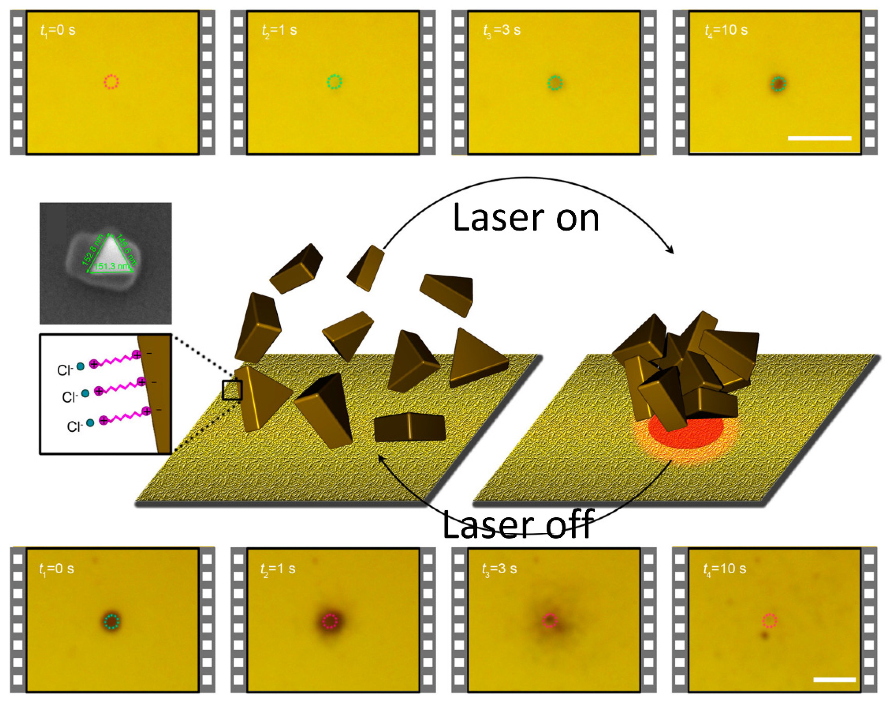
Optical manipulation of micro- and nanoscale particles in an optofluidic device has received increasing interest. Optical tweezers and near-field plasmonic tweezers are promising techniques that can be used for manipulating targets of interest in microfluidic systems. In conventional optical tweezers using a focused laser, the linear momentum of irradiated light can be directly transferred to the interacting objects, which creates the gradient and scattering forces to manipulate the object. Direct particle manipulation with optical tweezers involves strict requirements on the intensity and geometrical parameters of the focused light. Moreover, the conventional optical tweezers have an intrinsic barrier to reach the nanoscale spatial resolution due to the diffraction limit. By employing the plasmonic nanostructure, the gradient force of the conventional optical tweezers can be significantly amplified and localized near the vicinity of the nanostructures. Therefore, this so-called plasmonic near-field optical tweezer technology has been integrated into the optofluidic system for advanced imaging applications in recent years. The process of particle manipulation, e.g., trapping, transporting, assembly, and relocating, can be characterized by optofluidic-based imaging. Lin et al. proposed a scheme for the reversible assembly of gold nanotriangles (AuNTs) by switching the laser on and off to control the plasmon-enhanced thermophoresis [62]. The AuNTs presenting an average side length of 150 nm were dispersed in an aqueous cetyltrimethylammonium chloride (CTAC) solution to generate a positive and hydrophilic surface. Gold nanoislands (AuNIs) were formed on the substrate through gold film annealing. Thermophoresis arose from the temperature gradient to activate the assembly of AuNTs in the vicinity of AuNIs when illuminating the AuNIs using a low-power laser beam. The process of AuNT assembly and disassembly was captured by successive optical imaging, as shown in Figure 5. Furthermore, the authors demonstrated the parallel and dynamic manipulation of nanoparticles and employed the nanoparticle assembly for molecule sensing based on surface-enhanced Raman scattering (SERS). Ertsgaard and coworkers also proposed a rapid and label-free chemical analysis platform using the optofluidic near-field manipulation and Raman spectroscopy imaging techniques [63]. In that work, a nanogap-based plasmonic optofluidic platform combined with sub-volt dielectrophoretic trapping was used for surface-enhanced Raman imaging of biological nanoparticles. In another research work, Kang and coauthors utilized the gold nanoisland substrate and generated microbubbles to entrap the colloidal particles onto the interface [64]. This study demonstrated that the particle aggregation induced by microbubbles can enhance the SERS signal for imaging, which indicates the potential applications in low-cost optofluidic detection of chemical and biological molecules.
4. Optofluidic for Sensing Applications
4.1. Absorption Based Optofluidic Sensing
Characteristic absorption described as Lambert–Beer’s law (Equation (1)) is a fundamental phenomenon for chemical quantification and has been ubiquitously used in environmental, clinical, and biochemical analyses. Compared to the conventional 1 cm cell or 96-well plate based assays, the implementation of absorbance measurement in microfluidics has clear advantages in saving sample and reagent consumption, system miniaturization and integration, suitability for continuous-flow monitoring, and improved measurement performance.
where is absorbance, is the molar absorption coefficient, is the length of optical pathway, is the concentration.
The high sensitivity of absorbance measurement has been realized in microfluidics using a couple of strategies. The extension of microchannels represents one direct approach to enhance the sensitivity. Tang et al. employed two-photon stereolithography to fabricate a 3D-microlens-incorporating microfluidic chip for highly sensitive absorbance measurement, as shown in Figure 6a, in which the optical pathway was approximately 60 mm in a 3 µL channel and the sensitivity was improved by an order of magnitude compared to the 96-well based assay [7]. The incorporation of microlenses can significantly reduce the optical loss and improve the signal-to-noise ratio. Yang et al. designed a narrow channel with a 26 µm width following a main channel with a 150 µm width to extend the optical path length for a sensitive measurement of droplet absorbance [65]. In addition to the direct extension of the detection channel, a scheme of multiple reflection within microfluidics has also been used for sensitivity improvement. For example, Jordi et al. extended the optical path for cultured cell measurement via confining the light transmission in a zigzag path inside the chip using air mirrors [66], as shown in Figure 6b. Zhu et al. developed a portable phosphate sensor using a Fabry–Pérot cavity, in which the optical length was improved four-fold by multiple reflection between the cavity mirrors [67]. Bajuszova et al. added a pair of mirrors on the top and bottom of a microtiter plate and achieved a two-fold improvement in sensitivity for immunoassay measurement [68]. As the third strategy for sensitivity improvement, an evanescent field in the vicinity outside the coiled optical fiber was used to intensify the absorption. According to Mei’s research, as shown in Figure 6c, a nanofiber in a optofluidic chip achieved a 10-fold improvement in sensitivity compared to the result from a standard 1 cm absorption cuvette [43].
Throughput represents another relevant parameter to indicate the sensor performance. Parallel configuration of the light source and the photodetector is a common approach to enhance throughput. For example, Sieben et al. incorporated four light source/detector pairs in a chip for multichannel application in monitoring the reaction process and reagent mixing [69]. In addition to parallel configuration, Tang et al. developed a multichannel colorimetric analysis using on-chip optical switches, in which the LED light was guided to four bare optical fibers and the spectrometer read the spectrum data from four detection channels in sequence [28], as shown in Figure 6d. Imaging represents a high-throughput method for absorption measurement. It should be noted that, despite the high throughput originating from the charge coupled device (CCD) image, the resolution for adsorption characterization may be not sufficient. Shi et al. incorporated nine green-light LEDs in an optofluidic chip for the determination of nitrite using differential colorimetry, as shown in Figure 6e. In this detection system, a CCD was placed close to the bottom of chip to capture the light signal simultaneously emitted from the nine detection channels [70]. Interestingly, the absorbance was determined by the optofluidic differential colorimetry, representing a direct approach with little dependence on the calibration curve. By setting up a microfluidic split network, the mixture ratio of nitrite and reagents in each channel was different, leading to a gradient of signal intensity. The final concentration of nitrite could be calculated with a mean error of 0.50–1.16% according to the ratio of the slope values of the curves depicting the relationship between the absorbance, the channel number, and the concentration of the reagent added.
4.2. Reflection and Refraction Based Optofluidic Sensing
The RI difference in two media causes light reflection and refraction at their interface. According to Snell’s law and Fresnel equations, light transmittance and reflectance are dependent on the RI value of the media, as described in Equations (2)–(6).
where, and are the RI of medium 1 (incident light) and medium 2 (refracted light), and and are the incident angle and refracted angle, respectively. , , , and are the reflection and transmission coefficients for the s-polarized and p-polarized light, respectively. The medium is nonmagnetic.
This dependence lays the foundation for RI sensing and light manipulations in the optofluidic system. Because RI is a fundamental physical parameter closely related to the concentration or density of substances, as a non-invasive and label-free analysis approach, RI sensors have been used in industrial metrology [71,72], biochemical detection [12], and environmental analysis [73,74]. Compared to the RI sensors based on advanced interference and resonance structures, e.g., fiber Bragg grating (FBG) and photonic fiber crystal (PFC), reflection- and refraction-based RI sensors are usually based on intensity-modulation and have clear advantages in easy fabrication and low cost. For example, Zhang et al. provided a RI sensor with a low fabrication difficulty and a simple chip layout [75], as shown in Figure 7a. In the designed optofluidic chip, only fiber grooves and a flow channel were configured. As a response to the RI variations in the optofluidic channel, light intensity varied due to the change in the reflectance at the channel wall, and eventually received by the output optical fiber. Based on partial reflection, a wide dynamic range of 1.33–1.37 and a detection resolution 5 × 10⁻⁵ RIU (Refractive Index Unit) were achieved. Despite the wide dynamic range, the linearity of the calibration curve remained to be improved and the sensitivity decreased significantly at high RI values. Weber et al. employed a configuration similar to that of Zhang’s work, and the ratio of the reflected and transmitted light was used for characterizing the RI changes and the sample concentration [76]. The detection limit was approximately 5% phosphate. Barshilia et al. fabricated a planar waveguide-based optofluidic chip for low-cost RI sensing [77], as shown in Figure 7b. The core and the upper wall of the waveguide consisted of glass and samples, respectively. The alteration of sample RI changed the transmittance of light through the waveguide and caused a variation in light intensity. A limit of detection of approximately 1% (w/w) sodium chloride and a resolution of 5.7 × 10⁻⁴ RIU were realized. Although this prototype had a simple configuration and a low cost, the sensing performance remained to be improved. Tang et al. developed a 3D-microlens-cascade optofluidic chip (3DMCOC) for refractometry with adjustable sensitivity [33], as shown in Figure 7c. The convergence or divergence of the light bundle changed with the RI of the medium used to fill the 3D microlens cavity. The 3DMCOC achieved a resolution of 3.8 × 10⁻⁵ RIU using the seven-microlens configuration, and a wide dynamic range of 1.33–1.51 was realized using the single microlens configuration. Furthermore, the authors demonstrated the application of the 3DMCOC for the measurement of salinity and the specific gravity of urine. We provide a summary of reflection/refraction-based optofluidic RI sensors in terms of configuration and performance in Table 3. A resolution at 10−6–10−7 RIU using an intensity-modulation method remains a goal to achieve in the future. We envision the emergence of new optofluidic configurations to achieve this goal and sensitive applications of optofluidic RI sensors in more fields.
4.3. Scattering-Based Optofluidic Sensing
Scattering represents a forced deviation of light when passing through particles, and has been widely employed for cytometry and biochemical sensing in optofluidics [79,80,81]. Based on the forward scattering or the side scattering, properties of cells and particles can be captured. For example, Kunstnabb-Olsen et al. employed an integrated on-chip flow cytometer setup in which the splitting of nitrobenzene droplet at different hydrodynamic conditions in a microchannel was characterized by the scattered laser light [82]. Barat et al. designed a microfluidic cytometer based on simultaneous detection of scattered light, fluorescence, and impedance, in which a range of different sized polystyrene beads were used for system characterization [83]. Hengoju et al. designed an optofluidic detection setup to analyze microbiological samples in droplets in which three pairs of microlenses and optical fibers were incorporated to collect the signals of fluorescence, absorbance, and scattering [79], as shown in Figure 8a. In addition to scattering-based cytometry, SERS has been ubiquitously used as a sensitive sensing mechanism because the inelastic light scattering of the irradiated molecules can be significantly enhanced by the structured metal surface [84,85]. For example, Bai et al. fabricated 2D periodic copper–silver nanostructures inside a glass microfluidic chip for cadmium ion sensing with a limit of detection of 10 ppb [86], as shown in Figure 8b. Rickard et al. fabricated gold-coated nanopillars as the SERS-active substrate in an optofluidic chip for rapid biomarker detection of traumatic brain injury, with a detection limit at the picomolar level [80]. Choi et al. fabricated an integrated optofluidic SERS platform for the real-time characterization of airborne microorganisms [87], as shown in Figure 8c. In this system, the microorganisms in the air flow traveled across the liquid–gas phase boundary due to the inertial effect in the curved channel and were collected by the SERS-active fluid, which contained the colloidal silver nanoparticles. Then, the real-time SERS analysis was conducted on the sample optofluidic chip and the limit of detection was approximately 100 cfu (colony forming unit)/mL. Another recent study reported the use of micro-structured hollow fiber (MHF) for SERS-based adenine sensing and a limit of detection 10 fM was achieved [88].
4.4. Plasmonic Based Optofluidic Biosensing
LSPR represents an intense electromagnetic near-field coupling effect originating from noble-metal nanostructures. Such a coupling effect is related to the size, geometry, and materials of the nanostructures [89]. By optimizing these parameters, a strong electromagnetic near-field can be generated in the vicinity of the nanostructures. The susceptibility to the surrounding RI enables LSPR as a sensitive platform for monitoring biological binding events. LSPR-based biosensors using diverse materials and optical modulations have been increasingly reported. Liyanage et al. reported a tapered optical fiber (TOF)-based plasmonic biosensor in which gold triangular nanoprisms were coated as the transduction materials [90]. In human serum samples, microRNAs were successfully detected with a limit of detection at the fM scale. Kim et al. fabricated a 20 × 20 µm2 nanodisk array on the end face of the fiber core and employed it for LSPR-based prostate-specific antigen sensing, as shown in Figure 9a. [91] The nanostructured end-face was inserted into a microfluidic channel for real-time biosensing and the reported limit of detection was found to be 0.1 pg/mL. Qiu et al. proposed a strategy for the measurement of total bioaerosol-based LSPR [53], as shown in Figure 9b. The gold nanoislands were functionalized with succinimidyl ester, which can detect the bioaerosols by chemically reacting with the amine group. This strategy achieved a detection limit of approximately 1 cell/mL. The same system was further adapted to the quantification of the novel coronavirus during the COVID-19 pandemic. The optofluidic biosensing chip containing the 2D gold nanoisland array and microfluidic sensing chamber was employed for the sensitive detection of SARS-CoV-2 [52], as shown in Figure 9c. The gold nanoislands were functionalized with complementary DNA receptors to capture the selected virus sequence via nucleic acid hybridization. The hybridization caused a sensitive phase change for the target quantification. Above the optofluidic chip, an additional laser was set to stimulate the photothermal effect to regulate the nucleic acid hybridization and improve the detection sensitivity. A limit of detection 0.22 pM of the selected virus sequence was achieved. It is worthwhile to note that the optofluidic systems in Figure 9b,c are based on a common-path interferometric configuration. In fact, the interferometric configuration is a powerful approach to improve the sensitivity of optofluidics for biosensing and has attracted attention in other optofluidic sensing and imaging systems, e.g., optofluidic fiber optics [92]. Funari et al. employed a gold nanospike-coated glass as the detection substrate, as shown in Figure 9d. The gold nanospikes were functionalized by chemical crosslinking and immobilized with antigens as the target receptor. Each step of functionalization was validated by the change in the LSPR spectra in air. The LSPR spectra were recorded in a reflection mode with a sensitivity of 183 nm/RIU [55]. The detection limit of the antibody against the SARS-CoV-2 was as low as 0.5 pM. Other biosensing application cases using LSPR technology and optofluidic systems are summarized in Table 4, including the use of different optical modulation approaches such as wavelength, intensity, and phase for highly sensitive detection of disease biomarkers, extracellular vesicles, and the functionalities of bioactive macromolecules. Compared to the wavelength- and phase-based approaches, intensity modulation is a promising approach for low-cost LSPR biosensing devices despite a possible decrease in sensitivity. The development of novel optical materials and advanced nanofabrication technologies is driving the continuous innovation of plasmonic biosensing. By integrating with emerging microfluidic techniques, plasmonic-based optofluidic technologies will result in more breakthrough applications in the field of bioanalytical chemistry, biomedical engineering, and life science.
5. Conclusions and Perspectives
Optofluidic technologies, which integrate the novel development of photonic and microfluidic advances, have opened a new avenue for biochemical analysis. In order to better understand the current development in this direction, we reviewed the recent progress of optofluidic devices in fabrication techniques, imaging, and sensing applications. We hope the information in this concise review is useful for researchers working in optofluidic-related areas. From our perspective, a high-level integration of fluid controls (pump, valve, mixer, flow chamber, etc.), optical manipulation units (microlenses, micro waveguides, micromirrors, microprisms, photonic nanostructures, optical fibers, etc.), light sources (miniaturized LED, organic LED on a chip, etc.), and detectors (miniaturized spectrometer, photodiode, etc.) is still needed to make optofluidic chips compact and smart. These integrated optical and microfluidic controlling components can greatly improve the functionality of optofluidics. First, advanced optical and nanophotonic phenomena with different functions can be introduced into existing microfluidic systems, so as to improve the performance of existing optical biosensing and imaging devices; for instance, many optofluidic-based point-of-care (PoC) detection technologies developed during the current ongoing novel coronavirus (COVID-19) pandemic. The utilization of novel optofluidic technologies may greatly improve the performance of PoC detection. Second, the integration of microfluidics and micro-/nano-optics can be used to explore novel physical and chemical phenomena and applications; for example, in the micro-/nano-scale, the mechanical control exerted by light and fluid on the biosensing targets (bioanalytes) can be used for developing advanced optofluidic biosensing systems. In addition, a comprehensive improvement in resolution, throughput, and sensitivity by optimizing optical configuration, sensing materials, and data treatment will make a critical difference to the imaging and biosensing applications. Furthermore, programmable optofluidic system control, excellent compatibility between different optofluidic chips, and the multiplexing optofluidic sensing array, will result in a breakthrough for biochemical analysis.
Author Contributions
J.T. and G.Q. wrote the manuscript. J.W. supervised this work. All authors have read and agreed to the published version of the manuscript.
Funding
This research received no external funding.
Conflicts of Interest
The authors declare no conflict of interest.
References
- Yang, H.; Gijs, M.A. Micro-optics for microfluidic analytical applications. Chem. Soc. Rev. 2018, 47, 1391–1458. [Google Scholar] [CrossRef]
- Elvira, K.S.; Solvas, X.C.; Wootton, R.C.R.; de Mello, A.J. The past, present and potential for microfluidic reactor technology in chemical synthesis. Nat. Chem. 2013, 5, 905–915. [Google Scholar] [CrossRef]
- Zhang, J.; Yan, S.; Yuan, D.; Alici, G.; Nguyen, N.-T.; Ebrahimi Warkiani, M.; Li, W. Fundamentals and applications of inertial microfluidics: A review. Lab Chip 2016, 16, 10–34. [Google Scholar] [CrossRef] [PubMed] [Green Version]
- Atencia, J.; Beebe, D.J. Controlled microfluidic interfaces. Nature 2005, 437, 648–655. [Google Scholar] [CrossRef] [PubMed]
- Nge, P.N.; Rogers, C.I.; Woolley, A.T. Advances in Microfluidic Materials, Functions, Integration, and Applications. Chem. Rev. 2013, 113, 2550–2583. [Google Scholar] [CrossRef] [PubMed] [Green Version]
- Convery, N.; Gadegaard, N. 30 years of microfluidics. Micro Nano Eng. 2019, 2, 76–91. [Google Scholar] [CrossRef]
- Tang, J.; Qiu, G.; Cao, X.; Yue, Y.; Zhang, X.; Schmitt, J.; Wang, J. Self-aligned 3D microlenses in a chip fabricated with two-photon stereolithography for highly sensitive absorbance measurement. Lab Chip 2020, 20, 2334–2342. [Google Scholar] [CrossRef]
- Shen, Y.; Yalikun, Y.; Tanaka, Y. Recent advances in microfluidic cell sorting systems. Sens. Actuators B Chem. 2019, 282, 268–281. [Google Scholar] [CrossRef]
- Rothbauer, M.; Zirath, H.; Ertl, P. Recent advances in microfluidic technologies for cell-to-cell interaction studies. Lab Chip 2018, 18, 249–270. [Google Scholar] [CrossRef] [PubMed] [Green Version]
- Zhang, S.; Wang, Y.; Onck, P.; den Toonder, J. A concise review of microfluidic particle manipulation methods. Microfluid. Nanofluid. 2020, 24, 24. [Google Scholar] [CrossRef] [Green Version]
- Kaminski, T.S.; Garstecki, P. Controlled droplet microfluidic systems for multistep chemical and biological assays. Chem. Soc. Rev. 2017, 46, 6210–6226. [Google Scholar] [CrossRef] [PubMed] [Green Version]
- Fan, X.; White, I.M. Optofluidic microsystems for chemical and biological analysis. Nat. Photonics 2011, 5, 591. [Google Scholar] [CrossRef]
- Yang, H.; Gijs, M.A. Optofluidic Devices for Bioanalytical Applications. In Advanced MEMS/NEMS Fabrication and Sensors; Springer: Berlin/Heidelberg, Germany, 2022; pp. 247–282. [Google Scholar]
- Psaltis, D.; Quake, S.R.; Yang, C. Developing optofluidic technology through the fusion of microfluidics and optics. Nature 2006, 442, 381–386. [Google Scholar] [CrossRef]
- Zhu, J.; Zhu, X.; Zuo, Y.; Hu, X.; Shi, Y.; Liang, L.; Yang, Y. Optofluidics: The interaction between light and flowing liquids in integrated devices. Opto-Electron. Adv. 2019, 2, 190007. [Google Scholar] [CrossRef]
- Rodríguez-Ruiz, I.; Ackermann, T.N.; Muñoz-Berbel, X.; Llobera, A. Photonic Lab-on-a-Chip: Integration of Optical Spectroscopy in Microfluidic Systems. Anal. Chem. 2016, 88, 6630–6637. [Google Scholar] [CrossRef] [Green Version]
- Fernandez-Cuesta, I.; Llobera, A.; Ramos-Payán, M. Optofluidic systems enabling detection in real samples: A review. Anal. Chim. Acta 2021, 339307, in press. [Google Scholar] [CrossRef]
- Borrelli, N.F. Microoptics Technology: Fabrication and Applications of Lens Arrays and Devices; CRC Press: Boca Raton, FL, USA, 2017. [Google Scholar]
- Monaghan, T.; Harding, M.J.; Harris, R.A.; Friel, R.J.; Christie, S.D.R. Customisable 3D printed microfluidics for integrated analysis and optimisation. Lab Chip 2016, 16, 3362–3373. [Google Scholar] [CrossRef] [Green Version]
- Bhattacharjee, N.; Urrios, A.; Kang, S.; Folch, A. The upcoming 3D-printing revolution in microfluidics. Lab Chip 2016, 16, 1720–1742. [Google Scholar] [CrossRef] [Green Version]
- Au, A.K.; Huynh, W.; Horowitz, L.F.; Folch, A. 3D-Printed Microfluidics. Angew. Chem. Int. Ed. 2016, 55, 3862–3881. [Google Scholar] [CrossRef] [PubMed]
- Ku, X.; Zhang, Z.; Liu, X.; Chen, L.; Li, G. Low-cost rapid prototyping of glass microfluidic devices using a micromilling technique. Microfluid. Nanofluid. 2018, 22, 82. [Google Scholar] [CrossRef]
- Guckenberger, D.J.; de Groot, T.E.; Wan, A.M.D.; Beebe, D.J.; Young, E.W.K. Micromilling: A method for ultra-rapid prototyping of plastic microfluidic devices. Lab Chip 2015, 15, 2364–2378. [Google Scholar] [CrossRef] [PubMed] [Green Version]
- Hu, Y.; Rao, S.; Wu, S.; Wei, P.; Qiu, W.; Wu, D.; Xu, B.; Ni, J.; Yang, L.; Li, J.; et al. All-Glass 3D Optofluidic Microchip with Built-in Tunable Microlens Fabricated by Femtosecond Laser-Assisted Etching. Adv. Opt. Mater. 2018, 6, 1701299. [Google Scholar] [CrossRef]
- Nguyen, T.-Q.; Mah, J.; Park, W.-T.; Lee, S. Rapid and Versatile Micromold Fabrication Using Micromilling and Nanopolishing for Microfluidic Devices. In Proceedings of the ASME-JSME-KSME 2019 8th Joint Fluids Engineering Conference, San Francisco, CA, USA, 28 July–1 August 2019. [Google Scholar]
- Zhao, Y.-B.; Tang, J.; Cen, T.; Qiu, G.; He, W.; Jiang, F.; Yu, R.; Ludwig, C.; Wang, J. Integrated aerodynamic/electrochemical microsystem for collection and detection of nanogram-level airborne bioaccessible metals. Sens. Actuators B Chem. 2022, 351, 130903. [Google Scholar] [CrossRef]
- Lin, T.-Y.; Do, T.; Kwon, P.; Lillehoj, P.B. 3D printed metal molds for hot embossing plastic microfluidic devices. Lab Chip 2017, 17, 241–247. [Google Scholar] [CrossRef] [PubMed] [Green Version]
- Tang, J.; Cao, X.; Qiu, G.; deMello, A.; Wang, J. Optical-Switch-Enabled Microfluidics for Sensitive Multichannel Colorimetric Analysis. Anal. Chem. 2021, 93, 6784–6791. [Google Scholar] [CrossRef]
- Aćimović, S.S.; Ortega, M.A.; Sanz, V.; Berthelot, J.; Garcia-Cordero, J.L.; Renger, J.; Maerkl, S.J.; Kreuzer, M.P.; Quidant, R. LSPR Chip for Parallel, Rapid, and Sensitive Detection of Cancer Markers in Serum. Nano Lett. 2014, 14, 2636–2641. [Google Scholar] [CrossRef] [PubMed] [Green Version]
- Holzner, G.; Du, Y.; Cao, X.; Choo, J.; deMello, A.J.; Stavrakis, S. An optofluidic system with integrated microlens arrays for parallel imaging flow cytometry. Lab Chip 2018, 18, 3631–3637. [Google Scholar] [CrossRef]
- Kirchner, R.; Schift, H. Thermal reflow of polymers for innovative and smart 3D structures: A review. Mater. Sci. Semicond. Processing 2019, 92, 58–72. [Google Scholar] [CrossRef]
- Gissibl, T.; Thiele, S.; Herkommer, A.; Giessen, H. Two-photon direct laser writing of ultracompact multi-lens objectives. Nat. Photonics 2016, 10, 554–560. [Google Scholar] [CrossRef]
- Tang, J.; Qiu, G.; Zhang, X.; Wang, J. A 3D-cascade-microlens optofluidic chip for refractometry with adjustable sensitivity. Lab Chip 2021, 21, 3784–3792. [Google Scholar] [CrossRef]
- Cao, X.; Du, Y.; Küffner, A.; Van Wyk, J.; Arosio, P.; Wang, J.; Fischer, P.; Stavrakis, S.; deMello, A. A Counter Propagating Lens-Mirror System for Ultrahigh Throughput Single Droplet Detection. Small 2020, 16, 1907534. [Google Scholar] [CrossRef]
- Vanderpoorten, O.; Peter, Q.; Challa, P.K.; Keyser, U.F.; Baumberg, J.; Kaminski, C.F.; Knowles, T.P.J. Scalable integration of nano-, and microfluidics with hybrid two-photon lithography. Microsyst. Nanoeng. 2019, 5, 40. [Google Scholar] [CrossRef] [Green Version]
- Unger, M.A.; Chou, H.-P.; Thorsen, T.; Scherer, A.; Quake, S.R. Monolithic Microfabricated Valves and Pumps by Multilayer Soft Lithography. Science 2000, 288, 113–116. [Google Scholar] [CrossRef] [Green Version]
- Whitesides, G.M. The origins and the future of microfluidics. Nature 2006, 442, 368–373. [Google Scholar] [CrossRef] [PubMed]
- Zeng, S.; Li, B.; Su, X.o.; Qin, J.; Lin, B. Microvalve-actuated precise control of individual droplets in microfluidic devices. Lab Chip 2009, 9, 1340–1343. [Google Scholar] [CrossRef]
- Rho, H.S.; Yang, Y.; Terstappen, L.W.M.M.; Gardeniers, H.; Le Gac, S.; Habibović, P. Programmable droplet-based microfluidic serial dilutor. J. Ind. Eng. Chem. 2020, 91, 231–239. [Google Scholar] [CrossRef]
- Sun, Y.; Cai, B.; Wei, X.; Wang, Z.; Rao, L.; Meng, Q.-F.; Liao, Q.; Liu, W.; Guo, S.; Zhao, X. A valve-based microfluidic device for on-chip single cell treatments. Electrophoresis 2019, 40, 961–968. [Google Scholar] [CrossRef] [PubMed]
- Stavrakis, S.; Holzner, G.; Choo, J.; deMello, A. High-throughput microfluidic imaging flow cytometry. Curr. Opin. Biotechnol. 2019, 55, 36–43. [Google Scholar] [CrossRef] [PubMed]
- Yang, Y.; Liu, A.Q.; Lei, L.; Chin, L.K.; Ohl, C.D.; Wang, Q.J.; Yoon, H.S. A tunable 3D optofluidic waveguide dye laser via two centrifugal Dean flow streams. Lab Chip 2011, 11, 3182–3187. [Google Scholar] [CrossRef]
- Mei, H.; Pan, J.; Zhang, Z.; Zhang, L.; Tong, L. Coiled Optical Nanofiber for Optofluidic Absorbance Detection. ACS Sens. 2019, 4, 2267–2271. [Google Scholar] [CrossRef] [PubMed]
- Li, L.; Zhang, Y.-N.; Zhou, Y.; Zheng, W.; Sun, Y.; Ma, G.; Zhao, Y. Optical Fiber Optofluidic Bio-Chemical Sensors: A Review. Laser Photonics Rev. 2021, 15, 2000526. [Google Scholar] [CrossRef]
- Zhao, Y.; Hu, X.-G.; Hu, S.; Peng, Y. Applications of fiber-optic biochemical sensor in microfluidic chips: A review. Biosens. Bioelectron. 2020, 166, 112447. [Google Scholar] [CrossRef]
- Zhang, N.; Humbert, G.; Wu, Z.; Li, K.; Shum, P.P.; Zhang, N.M.Y.; Cui, Y.; Auguste, J.-L.; Dinh, X.Q.; Wei, L. In-line optofluidic refractive index sensing in a side-channel photonic crystal fiber. Opt. Express 2016, 24, 27674–27682. [Google Scholar] [CrossRef] [PubMed]
- Zhang, A.P.; Gao, S.; Yan, G.; Bai, Y. Advances in optical fiber Bragg grating sensor technologies. Optofluid. Refract. Index Sens. Based Partial. Reflect. 2012, 2, 1–13. [Google Scholar] [CrossRef] [Green Version]
- Li, Z.; Xu, Y.; Fang, W.; Tong, L.; Zhang, L. Ultra-Sensitive Nanofiber Fluorescence Detection in a Microfluidic Chip. Sensors 2015, 15, 4890–4898. [Google Scholar] [CrossRef] [PubMed] [Green Version]
- Yang, Y.; Liu, A.Q.; Chin, L.K.; Zhang, X.M.; Tsai, D.P.; Lin, C.L.; Lu, C.; Wang, G.P.; Zheludev, N.I. Optofluidic waveguide as a transformation optics device for lightwave bending and manipulation. Nat. Commun. 2012, 3, 651. [Google Scholar] [CrossRef] [PubMed] [Green Version]
- Nguyen, N.-T. Micro-optofluidic Lenses: A review. Biomicrofluidics 2010, 4, 031501. [Google Scholar] [CrossRef] [Green Version]
- Dietvorst, J.; Goyvaerts, J.; Ackermann, T.N.; Alvarez, E.; Muñoz-Berbel, X.; Llobera, A. Microfluidic-controlled optical router for lab on a chip. Lab Chip 2019, 19, 2081–2088. [Google Scholar] [CrossRef] [Green Version]
- Qiu, G.; Gai, Z.; Tao, Y.; Schmitt, J.; Kullak-Ublick, G.A.; Wang, J. Dual-Functional Plasmonic Photothermal Biosensors for Highly Accurate Severe Acute Respiratory Syndrome Coronavirus 2 Detection. ACS Nano 2020, 14, 5268–5277. [Google Scholar] [CrossRef] [Green Version]
- Qiu, G.; Yue, Y.; Tang, J.; Zhao, Y.-B.; Wang, J. Total Bioaerosol Detection by a Succinimidyl-Ester-Functionalized Plasmonic Biosensor To Reveal Different Characteristics at Three Locations in Switzerland. Environ. Sci. Technol. 2020, 54, 1353–1362. [Google Scholar] [CrossRef]
- Qiu, G.; Gai, Z.; Saleh, L.; Tang, J.; Gui, T.; Kullak-Ublick, G.A.; Wang, J. Thermoplasmonic-Assisted Cyclic Cleavage Amplification for Self-Validating Plasmonic Detection of SARS-CoV-2. ACS Nano 2021, 15, 7536–7546. [Google Scholar] [CrossRef]
- Funari, R.; Chu, K.-Y.; Shen, A.Q. Detection of antibodies against SARS-CoV-2 spike protein by gold nanospikes in an opto-microfluidic chip. Biosens. Bioelectron. 2020, 169, 112578. [Google Scholar] [CrossRef]
- Li, X.; Soler, M.; Szydzik, C.; Khoshmanesh, K.; Schmidt, J.; Coukos, G.; Mitchell, A.; Altug, H. Label-Free Optofluidic Nanobiosensor Enables Real-Time Analysis of Single-Cell Cytokine Secretion. Small 2018, 14, 1800698. [Google Scholar] [CrossRef] [PubMed]
- Nguyen, T.T.; Trinh, K.T.L.; Yoon, W.J.; Lee, N.Y.; Ju, H. Integration of a microfluidic polymerase chain reaction device and surface plasmon resonance fiber sensor into an inline all-in-one platform for pathogenic bacteria detection. Sens. Actuators B Chem. 2017, 242, 1–8. [Google Scholar] [CrossRef]
- Grover, W.H.; Ivester, R.H.C.; Jensen, E.C.; Mathies, R.A. Development and multiplexed control of latching pneumatic valves using microfluidic logical structures. Lab Chip 2006, 6, 623–631. [Google Scholar] [CrossRef] [PubMed]
- Lei, C.; Kobayashi, H.; Wu, Y.; Li, M.; Isozaki, A.; Yasumoto, A.; Mikami, H.; Ito, T.; Nitta, N.; Sugimura, T.; et al. High-throughput imaging flow cytometry by optofluidic time-stretch microscopy. Nat. Protoc. 2018, 13, 1603–1631. [Google Scholar] [CrossRef]
- Bak, S.; Kim, G.H.; Jang, H.; Kim, J.; Lee, J.; Kim, C.-S. Real-time SPR imaging based on a large area beam from a wavelength-swept laser. Opt. Lett. 2018, 43, 5476–5479. [Google Scholar] [CrossRef]
- Jahani, Y.; Arvelo, E.R.; Yesilkoy, F.; Koshelev, K.; Cianciaruso, C.; De Palma, M.; Kivshar, Y.; Altug, H. Imaging-based spectrometer-less optofluidic biosensors based on dielectric metasurfaces for detecting extracellular vesicles. Nat. Commun. 2021, 12, 3246. [Google Scholar] [CrossRef]
- Lin, L.; Peng, X.; Wang, M.; Scarabelli, L.; Mao, Z.; Liz-Marzán, L.M.; Becker, M.F.; Zheng, Y. Light-Directed Reversible Assembly of Plasmonic Nanoparticles Using Plasmon-Enhanced Thermophoresis. ACS Nano 2016, 10, 9659–9668. [Google Scholar] [CrossRef]
- Ertsgaard, C.T.; Wittenberg, N.J.; Klemme, D.J.; Barik, A.; Shih, W.-C.; Oh, S.-H. Integrated Nanogap Platform for Sub-Volt Dielectrophoretic Trapping and Real-Time Raman Imaging of Biological Nanoparticles. Nano Lett. 2018, 18, 5946–5953. [Google Scholar] [CrossRef]
- Kang, Z.; Chen, J.; Ho, H.-P. Surface-enhanced Raman scattering via entrapment of colloidal plasmonic nanocrystals by laser generated microbubbles on random gold nano-islands. Nanoscale 2016, 8, 10266–10272. [Google Scholar] [CrossRef]
- Yang, T.; Stavrakis, S.; deMello, A. A High-Sensitivity, Integrated Absorbance and Fluorescence Detection Scheme for Probing Picoliter-Volume Droplets in Segmented Flows. Anal. Chem. 2017, 89, 12880–12887. [Google Scholar] [CrossRef]
- Vila-Planas, J.; Fernández-Rosas, E.; Ibarlucea, B.; Demming, S.; Nogués, C.; Plaza, J.A.; Domínguez, C.; Büttgenbach, S.; Llobera, A. Cell analysis using a multiple internal reflection photonic lab-on-a-chip. Nat. Protoc. 2011, 6, 1642–1655. [Google Scholar] [CrossRef] [PubMed]
- Zhu, J.; Han, G.; Hu, X.; Zuo, Y.; Chen, L.; Wang, F.; Yang, Y.; Jiang, F.; Sun, C.; Zhao, W.; et al. A Portable and Accurate Phosphate Sensor Using a Gradient Fabry–Pérot Array. ACS Sens. 2020, 5, 1381–1388. [Google Scholar] [CrossRef] [PubMed]
- Bajuszova, Z.; Ali, Z.; Scott, S.; Seetohul, L.N.; Islam, M. Cavity-Enhanced Immunoassay Measurements in Microtiter Plates Using BBCEAS. Anal. Chem. 2016, 88, 5264–5270. [Google Scholar] [CrossRef] [PubMed] [Green Version]
- Sieben, V.J.; Floquet, C.F.; Ogilvie, I.R.; Mowlem, M.C.; Morgan, H. Microfluidic colourimetric chemical analysis system: Application to nitrite detection. Anal. Methods 2010, 2, 484–491. [Google Scholar] [CrossRef]
- Shi, Y.; Liu, H.L.; Zhu, X.Q.; Zhu, J.M.; Zuo, Y.F.; Yang, Y.; Jiang, F.H.; Sun, C.J.; Zhao, W.H.; Han, X.T. Optofluidic differential colorimetry for rapid nitrite determination. Lab Chip 2018, 18, 2994–3002. [Google Scholar] [CrossRef]
- Seki, A.; Narita, K.; Watanabe, K. Refractive Index Measurement in Sucrose Solution and Beverage Using Surface Plasmon Resonance Sensor Based on Hetero-core Structured Fiber Optic. Procedia Chem. 2016, 20, 115–117. [Google Scholar] [CrossRef] [Green Version]
- Muchtaridi, M.; Musfiroh, I.; Hambali, N.N.; Indrayati, W. Determination of alcohol contents of fermentated black tape ketan based on different fermentation time using specific gravity, refractive index and GC-MS methods. J. Microbiol. Biotechnol. Food Sci. 2020, 2020, 933–946. [Google Scholar]
- Chen, J.; Guo, W.; Xia, M.; Li, W.; Yang, K. In situ measurement of seawater salinity with an optical refractometer based on total internal reflection method. Opt. Express 2018, 26, 25510–25523. [Google Scholar] [CrossRef]
- Qian, Y.; Zhao, Y.; Wu, Q.-L.; Yang, Y. Review of salinity measurement technology based on optical fiber sensor. Sens. Actuators B Chem. 2018, 260, 86–105. [Google Scholar] [CrossRef]
- Zhang, L.; Zhang, Z.; Wang, Y.; Ye, M.; Fang, W.; Tong, L. Optofluidic Refractive Index Sensor Based on Partial Reflection. Photonic Sens. 2017, 7, 97. [Google Scholar] [CrossRef] [Green Version]
- Weber, E.; Vellekoop, M.J. Optofluidic micro-sensors for the determination of liquid concentrations. Lab Chip 2012, 12, 3754–3759. [Google Scholar] [CrossRef] [PubMed]
- Barshilia, D.; Chau, L.-K.; Chang, G.-E. Low-cost planar waveguide-based optofluidic sensor for real-time refractive index sensing. Opt. Express 2020, 28, 27337–27345. [Google Scholar] [CrossRef]
- Chao, K.-S.; Lin, T.-Y.; Yang, R.-J. Two optofluidic devices for the refractive index measurement of small volume of fluids. Microfluid. Nanofluid. 2012, 12, 697–704. [Google Scholar] [CrossRef]
- Hengoju, S.; Wohlfeil, S.; Munser, A.S.; Boehme, S.; Beckert, E.; Shvydkiv, O.; Tovar, M.; Roth, M.; Rosenbaum, M.A. Optofluidic detection setup for multi-parametric analysis of microbiological samples in droplets. Biomicrofluidics 2020, 14, 024109. [Google Scholar] [CrossRef] [PubMed]
- Rickard, J.J.S.; Di-Pietro, V.; Smith, D.J.; Davies, D.J.; Belli, A.; Oppenheimer, P.G. Rapid optofluidic detection of biomarkers for traumatic brain injury via surface-enhanced Raman spectroscopy. Nat. Biomed. Eng. 2020, 4, 610–623. [Google Scholar] [CrossRef]
- Yang, R.-J.; Fu, L.-M.; Hou, H.-H. Review and perspectives on microfluidic flow cytometers. Sens. Actuators B Chem. 2018, 266, 26–45. [Google Scholar] [CrossRef]
- Kunstmann-Olsen, C.; Hanczyc, M.M.; Hoyland, J.; Rasmussen, S.; Rubahn, H.-G. Uniform droplet splitting and detection using Lab-on-Chip flow cytometry on a microfluidic PDMS device. Sens. Actuators B Chem. 2016, 229, 7–13. [Google Scholar] [CrossRef]
- Barat, D.; Spencer, D.; Benazzi, G.; Mowlem, M.C.; Morgan, H. Simultaneous high speed optical and impedance analysis of single particles with a microfluidic cytometer. Lab Chip 2012, 12, 118–126. [Google Scholar] [CrossRef]
- Langer, J.; Jimenez de Aberasturi, D.; Aizpurua, J.; Alvarez-Puebla, R.A.; Auguié, B.; Baumberg, J.J.; Bazan, G.C.; Bell, S.E.J.; Boisen, A.; Brolo, A.G.; et al. Present and Future of Surface-Enhanced Raman Scattering. ACS Nano 2020, 14, 28–117. [Google Scholar] [CrossRef] [Green Version]
- Pilot, R.; Signorini, R.; Durante, C.; Orian, L.; Bhamidipati, M.; Fabris, L. A Review on Surface-Enhanced Raman Scattering. Biosensors 2019, 9, 57. [Google Scholar] [CrossRef] [Green Version]
- Bai, S.; Serien, D.; Hu, A.; Sugioka, K. 3D Microfluidic Surface-Enhanced Raman Spectroscopy (SERS) Chips Fabricated by All-Femtosecond-Laser-Processing for Real-Time Sensing of Toxic Substances. Adv. Funct. Mater. 2018, 28, 1706262. [Google Scholar] [CrossRef]
- Choi, J.; Lee, J.; Jung, J.H. Fully integrated optofluidic SERS platform for real-time and continuous characterization of airborne microorganisms. Biosens. Bioelectron. 2020, 169, 112611. [Google Scholar] [CrossRef] [PubMed]
- Gao, D.; Yang, X.; Teng, P.; Kong, D.; Liu, Z.; Yang, J.; Luo, M.; Li, Z.; Wen, X.; Yuan, L.; et al. On-line SERS detection of adenine in DNA based on the optofluidic in-fiber integrated GO/PDDA/Ag NPs. Sens. Actuators B Chem. 2021, 332, 129517. [Google Scholar] [CrossRef]
- Mayer, K.M.; Hafner, J.H. Localized Surface Plasmon Resonance Sensors. Chem. Rev. 2011, 111, 3828–3857. [Google Scholar] [CrossRef] [PubMed]
- Liyanage, T.; Lai, M.; Slaughter, G. Label-free tapered optical fiber plasmonic biosensor. Anal. Chim. Acta 2021, 1169, 338629. [Google Scholar] [CrossRef]
- Kim, H.-M.; Uh, M.; Jeong, D.H.; Lee, H.-Y.; Park, J.-H.; Lee, S.-K. Localized surface plasmon resonance biosensor using nanopatterned gold particles on the surface of an optical fiber. Sens. Actuators B Chem. 2019, 280, 183–191. [Google Scholar] [CrossRef]
- Yuan, T.; Yang, X.; Liu, Z.; Yang, J.; Li, S.; Kong, D.; Qi, X.; Yu, W.; Long, Q.; Yuan, L. Optofluidic in-fiber interferometer based on hollow optical fiber with two cores. Opt. Express 2017, 25, 18205–18215. [Google Scholar] [CrossRef]
- Roether, J.; Chu, K.-Y.; Willenbacher, N.; Shen, A.Q.; Bhalla, N. Real-time monitoring of DNA immobilization and detection of DNA polymerase activity by a microfluidic nanoplasmonic platform. Biosens. Bioelectron. 2019, 142, 111528. [Google Scholar] [CrossRef] [PubMed]
- Oh, B.-R.; Huang, N.-T.; Chen, W.; Seo, J.H.; Chen, P.; Cornell, T.T.; Shanley, T.P.; Fu, J.; Kurabayashi, K. Integrated Nanoplasmonic Sensing for Cellular Functional Immunoanalysis Using Human Blood. ACS Nano 2014, 8, 2667–2676. [Google Scholar] [CrossRef] [PubMed]
- Maity, S.; Ghosh, S.; Bhuyan, T.; Das, D.; Bandyopadhyay, D. Microfluidic Immunosensor for Point-of-Care-Testing of Beta-2-Microglobulin in Tear. ACS Sustain. Chem. Eng. 2020, 8, 9268–9276. [Google Scholar] [CrossRef]
- Lv, X.; Geng, Z.; Su, Y.; Fan, Z.; Wang, S.; Fang, W.; Chen, H. Label-Free Exosome Detection Based on a Low-Cost Plasmonic Biosensor Array Integrated with Microfluidics. Langmuir 2019, 35, 9816–9824. [Google Scholar] [CrossRef] [PubMed]
Figure 1.
Direct manufacture of optofluidic devices using techniques: (a) 3D printing, (b) micromilling, (c) direct laser writing. (a) Reprinted with permission from ref [19], Copyright 2016, Royal Society of Chemistry; (b) Reprinted with permission from ref [22], Copyright 2018, Springer; (c) Reprinted with permission from ref [24], Copyright 2018.

Figure 2.
Mold replication for fabricating optofluidic devices. (a) Metal 3D printing for mold fabrication and hot embossing for replicating mold structures. (b) UV lithography for mold fabrication. (c) Two-photon stereolithography for mold fabrication and PDMS casting for replicating mold structures. (a) Reprinted with permission from ref [27], Copyright 2017, Royal Society of Chemistry; (b) Reprinted with permission from ref [28] Copyright 2021, American Chemical Society; (c) Reprinted with permission from ref [33], Copyright 2021, Royal Society of Chemistry.

Figure 3.
High-throughput cytometry imaging. (a) Optofluidic time-stretch microscopy for high-throughput cell imaging. (b) Microlens array-incorporated optofluidic chip for high-throughput imaging of cells. (c) Microlens array fabricated with two-photon stereolithography for high-throughput imaging of fluorescent droplets. (a) Reprinted with permission from ref [59], Copyright 2018, Nature Publishing Group; (b) reprinted with permission from ref [30], Copyright 2018, Royal Society of Chemistry; (c) reprinted with permission from ref [34], Copyright 2018, Wiley-VCH GmbH.

Figure 4.
Optofluidic imaging of biochemical analysis. (a) Real-time SRP imaging using a wavelength-swept laser with a large area. (b) Biosensing according to the reconstructed spectral shift derived from the optimal linear estimator algorithm and the time-resolved intensity images. (a) Reprinted with permission from ref [60], Copyright 2018, OPTICA Publishing Group. (b) Reprinted with permission from ref [61], Copyright 2021, Nature Publishing Group.

Figure 5.
Reversible assembly of plasmonic nanoparticles via optical manipulation. Reprinted with permission from ref [62], Copyright 2016, American Chemical Society.
Figure 5.
Reversible assembly of plasmonic nanoparticles via optical manipulation. Reprinted with permission from ref [62], Copyright 2016, American Chemical Society.

Figure 6.
Optofluidic devices for absorption applications. (a) Three-dimensional microlens incorporated in a chip with an extended optical pathway. (b) Multiple reflections in a channel. (c) Evanescent field-based absorption using a coiled fiber. (d) Optical-switch-enabled four-channel colorimetric analysis. (e) Differential colorimetry for the determination of nitrite concentration, eliminating the requirement of calibration curves. (a) Reprinted with permission from ref [7] Copyright 2020, Royal Society of Chemistry; (b) reprinted with permission from ref [66], Copyright 2011, Nature Publishing Group; (c) reprinted with permission from ref [43], Copyright 2019, American Chemical Society; (d) reprinted with permission from ref [28], Copyright 2021, American Chemical Society; (e) reprinted with permission from ref [70], Copyright 2018, Royal Society of Chemistry.

Figure 7.
Optofluidic reflection and refraction for RI sensing. (a) TIR in a waveguide. (b) Reflection at the channel wall. (c) Refraction through a microlens or cascaded multiple microlenses. (a) Reprinted with permission from ref [75] Copyright 2017, Springer; (b) Reprinted with permission from ref [77], Copyright 2020, OSA Publishing; (c) Reprinted with permission from ref [33], Copyright 2021, Royal Society of Chemistry.

Figure 8.
Optofluidic sensing based on light scattering. (a) Biological sample sensing in droplets in a cytometer. SERS-based sensing: (b) cadmium ion and (c) airborne microorganisms. (a) Reprinted with permission from ref [79] Copyright 2020, AIP publishing; (b) Reprinted with permission from ref [86], Copyright 2018, Wiley-VCH; (c) Reprinted with permission from ref [87], Copyright 2020, Elsevier.

Figure 9.
Optofluidic LSPR for the determination of (a) prostate specific antigens, (b) total bioaerosols, (c) sequence of the COVID-19 virus, and (d) antibodies against SARS-CoV-2. (a) Reprinted with permission from ref [91] Copyright 2019, Elsevier; (b) reprinted with permission from ref [53], Copyright 2020, American Chemical Society; (c) reprinted with permission from ref [52], Copyright 2020, American Chemical Society; (d) reprinted with permission from ref [55], Copyright 2020, Elsevier.


Table 1.
Techniques for microfluidic chip fabrication.
| Ref. | Techniques | Applications | Advantages | Disadvantages |
|---|---|---|---|---|
| [28] | UV lithography | Mold fabrication | High efficiency Large working area | Normally for 2D planar structure |
| [7,28,33] | Two-photon stereolithography | Mold fabrication Integrated optical components | High resolution Complicated structures | Low efficiency for large optofluidic structures |
| [19,27] | 3D printing | Mold fabrication Chip fabrication | Complicated structures | Limited choice of material |
| [22,23,25] | Micromilling | Mold fabrication Chip fabrication | Complicated structures Optional material | Low resolution |
| [24] | Direct laser writing | Chip fabrication Integrated optical components | High resolution Complicated structures | Low efficiency |
| [27] | Hot embossing | Chip fabrication | High efficiency | Low resolution |
| Mold injection | Chip fabrication | High efficiency | Low resolution |
Table 2.
Key components in optofluidic chips.
| Optofluidic Components | Functions | Ref |
|---|---|---|
| Valve | Fluid control | [28,36,37,38,39,40] |
| Hydraulic structure | Micro object focus; Optical reconfiguration | [41,42] |
| Optical fiber | Light guidance; Sensing substrate | [7,28,33,43,44,45] |
| Microlens | Light collection; Light collimation; Imaging | [7,24,30,34] |
| Micromirror | Light collection; Modulation of light direction | [34,51] |
| Waveguide | Light guidance; Optical reconfiguration | [49] |
| Photonic nanostructure | Imaging; Sensing | [52,53,54,55,56,57] |
Table 3.
Comparison of the intensity-modulation-based optofluidic RI sensor in terms of configuration and performance.
Table 3.
Comparison of the intensity-modulation-based optofluidic RI sensor in terms of configuration and performance.
| Ref. | Transduction Mechanism | Limit of Detection | Resolution | Detection Range |
|---|---|---|---|---|
| [78] | Refraction through a prism | Not mentioned | 5.0 × 10⁻³ RIU | 1.33–1.52 |
| [75] | Reflection at the interface | Not mentioned | 5.0 × 10⁻⁵ RIU | 1.33–1.37 |
| [77] | TIR in a waveguide | 1% (w/w) NaCl | 5.7 × 10⁻⁴ RIU | 1.33–1.38 |
| [76] | Reflection and refraction at the interface | 5% (w/w) phosphate | 1.6% phosphate | 1.33–1.44 |
| [33] | Refraction through microlenses | 0.04% (w/w) NaCl | 3.8 × 10⁻⁵ RIU | 1.33–1.51 |
Table 4.
Comparison of LSPR configuration and sensing performance.
| Ref. | Nanostructure and Substrate | Mode | Modulation | Limit of Detection |
|---|---|---|---|---|
| [91] | Gold nanodisks on fiber core | Reflection | Intensity | Prostate specific antigen: 0.1 pg/ml |
| [52,53,54] | Gold nanoislands on glass | TIR | Phase | Total bioaerosol: 0.5–1.7 cfu/mL Virus sequence: 0.22 pM |
| [55] | Gold nanospikes on glass | Transmission | Wavelength | Antibody: 0.5 pM |
| [93] | Mushroom-like gold Nanoparticles on silicon wafer | Reflection | Wavelength | Polymerase: 0.0625 U/mL |
| [94] | Gold nanoparticle on Zeonor surface | Reflection | Wavelength | Number of THP-1 cell for detecting TNF-α secretion: 533 |
| [95] | Gold nanoparticle colloidals in water | Transmission | Intensity | β-2-microglobulin (B2M): 100 fg/mL |
| [96] | Gold nano-ellipsoid array on quartz | Transmission | Wavelength | Exosomes CD63 biomarker: 1 ng/mL |
Publisher’s Note: MDPI stays neutral with regard to jurisdictional claims in published maps and institutional affiliations. |
© 2022 by the authors. Licensee MDPI, Basel, Switzerland. This article is an open access article distributed under the terms and conditions of the Creative Commons Attribution (CC BY) license (https://creativecommons.org/licenses/by/4.0/).
Share and Cite
MDPI and ACS Style
Tang, J.; Qiu, G.; Wang, J. Recent Development of Optofluidics for Imaging and Sensing Applications. Chemosensors 2022, 10, 15. https://0-doi-org.brum.beds.ac.uk/10.3390/chemosensors10010015
AMA Style
Tang J, Qiu G, Wang J. Recent Development of Optofluidics for Imaging and Sensing Applications. Chemosensors. 2022; 10(1):15. https://0-doi-org.brum.beds.ac.uk/10.3390/chemosensors10010015
Chicago/Turabian StyleTang, Jiukai, Guangyu Qiu, and Jing Wang. 2022. "Recent Development of Optofluidics for Imaging and Sensing Applications" Chemosensors 10, no. 1: 15. https://0-doi-org.brum.beds.ac.uk/10.3390/chemosensors10010015
Note that from the first issue of 2016, this journal uses article numbers instead of page numbers. See further details here.