Article

Effect of UV Irradiation on the Growth of ZnO:Er Nanorods and Their Intrinsic Defects

by
Maksym Buryi
1,*,
Katarína Ridzoňová
1,2,
Neda Neykova
1,3,
Lucie Landová
1,3,
František Hájek
1,4,
Vladimir Babin
1,
Kateřina Děcká
1,4,
Rupendra Kumar Sharma
3 and
Ognen Pop-Georgievski
5
1
FZU—Institute of Physics of the Czech Academy of Sciences, Na Slovance 1999/2, 182 00 Prague, Czech Republic
2
Faculty of Mathematics and Physics, Institute of Physics, Charles University, Ke Karlovu 5, 121 16 Prague, Czech Republic
3
Centre for Advanced Photovoltaics, Faculty for Electrical Engineering, Czech Technical University in Prague, Technická 2, 166 27 Prague, Czech Republic
4
Faculty of Nuclear Sciences and Physical Engineering, Czech Technical University in Prague, Břehová 7, 115 19 Prague, Czech Republic
5
Department of Chemistry and Physics of Surfaces and Interfaces, Institute of Macromolecular Chemistry, Czech Academy of Sciences, Heyrovský Sq. 2, 162 06 Prague, Czech Republic
*
Author to whom correspondence should be addressed.
Submission received: 30 December 2022 / Revised: 17 February 2023 / Accepted: 18 February 2023 / Published: 23 February 2023
(This article belongs to the Special Issue Advances in Magnetic Sensors with Nanocomponents)

Abstract

:
Nanorods of erbium-doped zinc oxide (ZnO:Er) were fabricated using a hydrothermal method. One batch was prepared with and another one without constant ultraviolet (UV) irradiation applied during the growth. The nanorods were free-standing (FS) as well as deposited onto a fused silica glass substrate (GS). The goal was to study the atomistic aspects influencing the charge transport of ZnO nanoparticles, especially considering the differences between the FS and GS samples. We focused on the excitons; the intrinsic defects, such as zinc interstitials, zinc vacancies, and related shallow donors; and the conduction electrons. UV irradiation was applied for the first time during the ZnO:Er nanorod growth. This led to almost total exciton and zinc vacancy luminescence reduction, and the number of shallow donors was strongly suppressed in the GS samples. The effect was much less pronounced in the FS rods. Moreover, the exciton emission remained unchanged there. At the same time, the Er3+ content was decreased in the FS particles grown under constant UV irradiation while Er3+ was not detected in the GS particles at all. These phenomena are explained.

Graphical Abstract

1. Introduction

ZnO is unique due to its wide direct bandgap (3.37 eV), high thermal conductivity (50 W/mK), and high exciton binding energy (60 meV at 300 K) [1,2,3]. In addition to that, ZnO exhibits anticorrosion [4,5] and antimicrobial properties [6,7,8] that have been implemented in a range of applications, including photovoltaics, photocatalysis [9,10,11,12], metal waste disposal technologies [13], light-emitting diodes (LED), scintillators, and nanomedicine [14,15,16,17]. Moreover, ZnO has been proposed as a promising material for gas sensors.
Regarding gas sensors, the sensing abilities of the semiconductor are governed by the changes in its conductivity due to the interaction with surrounding pollutants. The ZnO conductivity, in particular, is affected by the surface shallow donors which are exceedingly sensitive to the local surface modification. Note that the electron paramagnetic resonance (EPR) spectra of ZnO, in most cases, contain a shallow donor signal measured at the g factor g~1.96 (see, e.g., [18,19]). Different papers have assigned this signal to zinc interstitials [20,21], hydrogen interstitials [22], or shallow Ga(Al) donors [23,24,25,26]. In addition, the g = 2.0048 signal can be observed from the shallow donors at the ZnO nanoparticle surface [27,28,29,30,31,32,33]. Both g = 1.96 and g = 2.0048 signals changed with changing temperature, atmosphere, and laser light [34]. Such material instability also puts constraints on the sensor’s implementation [35,36].
The sensors can be activated and, therefore, improved by exposure to UV light as it is a way of lowering the power supply magnitude [37]. Such apparatuses are functional even at room temperature [37,38,39]. The physical background of this effect is the improvement of charge carrier transport. A clear indication of this phenomenon can be given by the exciton emission in ZnO nanorods. Therefore, along with the abovementioned shallow donor EPR signals, exciton luminescence [40] serves as a probe for the sensing abilities of the ZnO nanorods at the atomistic level. At the same time, exciton emission and consequently charge transport are negatively affected by the existence of native defects in the ZnO host which also contribute to their own emission appearance, within the 1–2 eV spectral region [22,32,41,42]. Typical defects are zinc and oxygen vacancies (VZn and VO, respectively) and related defects [18,19,22,42,43,44,45,46,47]. Therefore, to develop a good sensor, the feedback to the technology should be given based on the number of VZn and VO in the ZnO host. Their presence can be proven by luminescence and EPR measurements.
The use of ZnO at the nanoscale brings important benefits. ZnO nanorods are compact, offer a variety of architectures, and possess a high surface-to-volume ratio leading to pronounced sensitivity [48,49,50]. The fabrication of nanomaterial-based sensing devices is usually difficult and requires high investments [50,51]. However, ZnO nanorods can be fabricated by the hydrothermal growth (HT) method [52,53,54,55,56,57] which is based on a water solution. HT is cheap, and the number of architectures can be created by choosing certain additives such as hexamethylenetetramine (HMTA), ethylenediamine (EDA), polyethyleneimine (PEI), and others. The growth conditions of the ZnO nanorods are also critical since the concentration of precursors and their age, dopant concentration, and temperature and time of the reaction strongly influence the size, quality, luminescence, shallow donor levels, and, as a result, charge transport abilities critical for sensing characteristics [52,58,59,60,61]. Doping with erbium opens the path for UV exciton emission performance improvement, making ZnO:Er promising as a material for the ultrafast scintillating detectors used in, e.g., time-of-flight positron emission tomography (TOFPET) [62,63]. Moreover, erbium is also used in upconversion phenomena [64,65,66] which are helpful in the processes of charge and energy transfer. Note that Er contributes to the enhancement of charge carrier transport [67] leading to improved gas sensing [14,34,35,36,37]. There are plenty of studies on HT-grown erbium-doped free-standing zinc oxide nanoparticles [59,68,69,70,71]. However, to the best of our knowledge, there are no studies in the literature on ZnO:Er nanorod arrays deposited onto the quartz substrate. Moreover, there are no papers dedicated to the study of the ZnO:Er nanorods, including luminescence, grown under constant UV irradiation, both free-standing and deposited on the substrate. The charge carrier’s production and defect creation processes as well as their mutual influence and luminescence are thus not fully known in the ZnO:Er nanoparticles grown under UV. These aspects are critical for understanding ZnO nanostructures’ sensing abilities and provide feedback to the technologists engaged in the field of sensor manufacturing.
The present study is dedicated to the synthesis and detailed investigation of ZnO:Er nanoparticles simultaneously grown as deposited arrays and free-standing nanorods and applying constant UV irradiation during the growth. Numerous techniques, including X-ray diffraction, scanning electron microscopy, luminescence (including spatial correlation), and EPR methods were applied. The main idea is to reveal the influence of the morphology and the UV irradiation during growth on the atomistic aspects of the charge carriers’ production through the excitons and native defect creation. The path for the charge transport improvement and defect suppression to increase the potential of ZnO nanostructure application in sensors and scintillating detectors is discussed.

2. Experimental Section

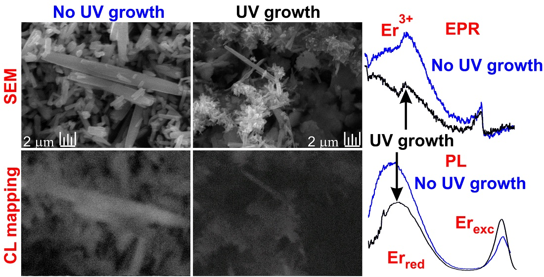
2.1. Sample Preparation: ZnO:Er Nanorods Deposited on a Quartz Substrate

The sample preparation procedure consisted of two steps (see Figure 1). First, the 70 nm thick nucleation layer of ZnO thin film was deposited on commercially available 1-inch2 fused silica glass substrate by pulse laser deposition (PLD). With this purpose, the substrate was placed onto a holder heated to 100 °C within a vacuum chamber. After pumping the chamber out and reaching a pressure of 10−4 Pa, oxygen was administered to the chamber to obtain the process pressure of 10 Pa. To reach the homogeneous spreading of the nucleation layer over the whole available area of the substrate, the sample holder rotated with an angular velocity of 5 rpm. After that, the pulse KrF excimer laser COMPex 50, operating at λ = 248 nm wavelength, was used for the bulk ZnO target ablation to cover the rotating substrate with the droplets of melted ZnO, which was then merged into a continuous layer. The pulse energy was set to 120 mJ, the number of pulses to 20,000, and the repetition rate to 30 Hz. Cooling of the prepared nucleation layer by introducing oxygen with a pressure of 105 Pa followed the deposition.
Second, the substrates with the deposited ZnO seeding layers prepared by the PLD method as described above were plunged into the aqueous solution containing 25 mmol/L of hexamethylene tetramine and 25 mmol/L of the mixture of zinc nitrate hexahydrate and erbium nitrate pentahydrate. The content of erbium corresponded to 0.05 and 0.25 mol%, respectively. The solution was kept at 90 °C for 3 h. After that, the substrate with the deposited ZnO:Er(0.05 and 0.25%) nanorods was removed from the solution, rinsed with deionized water, and dried in the nitrogen flow.
For the growth under UV, the substrates were mounted upside down on a flat-bottom quartz tube with an optical fiber placed inside the tube (a light source operating at 365 nm wavelength and 1 W power was used).

2.2. Sample Preparation: Free-Standing ZnO:Er Nanorods

The abovementioned aqueous solution also contained remnants of the not fully dissolved precursors or dust particles. These can serve as random nucleation centers, and therefore the process of ZnO:Er nanorod growth described in the second step in the subsection above also took place on these seeds. The ZnO rods grown in this way are free-standing particles. To compare the properties of the deposited nanorods with the properties of the free-standing ones grown under the same conditions, the solution was cooled down to ambient temperature after the abovementioned second step. Then, the free-standing nanorods remaining in the solution (see Figure 1) were isolated and washed 5 times with distilled water (removal of residual salts). After stirring for 15 min, they were filtered out using Whatman 2.
Based on the type of nanorods, either deposited on a substrate (GS) or free-standing (FS), grown under constant UV irradiation (UV) or without it, the samples were referred to in the text in the following way: ZnO:Er(0.05, 0.25%) GS UV, ZnO:Er(0.05, 0.25%) FS UV, ZnO:Er(0.05, 0.25%) GS, and ZnO:Er(0.05, 0.25%) FS. It should be noted that the 0.05 and 0.25% Er doping levels were chosen intentionally since the real concentration of erbium was 0.05% at the doping level of 0.05 mol% whereas the 0.5 mol% doping level resulted in a 0.25% real Er concentration in the free-standing ZnO:Er nanorods [32].
The samples were hexagonal nanorods. In general, the deposited nanoparticles were about more than one order of magnitude smaller, indicating a larger surface-to-volume ratio.

2.3. Experimental Techniques

X-ray diffraction (XRD) patterns were obtained within the 20–80° range of angles (a step of 0.02° and a scanning rate of 2°/min were used) on a Rigaku Miniflex 600 diffractometer (Rigaku, Tokyo, Japan) coupled with the Cu X-ray tube operating at a wavelength Kα1,2 of 0.15418 nm, a voltage of 40 kV, and a current of 15 mA. The ICDD PDF-2 database (version 2013) was used for comparison. To complement the data obtained using XRD, scanning electron microscopy (SEM) was used to test the samples for their shape and size on a MAIA3, TESCAN electron microscope. The in-beam SE detector was situated in an objective lens. The energy of the electron beam was 5 keV.
Luminescence characteristics were investigated by two techniques. (i) Photoluminescence (PL) was measured on a homemade spectrometer composed of: (a) pulsed UV light-emitting diode (LED) operating at 340 nm wavelength and 1 mW power; (b) a narrow band-pass optical filter; (c) a Peltier cooled photomultiplier sensitive in the 355–800 nm spectral range (2 nm spectral resolution); (d) a spectrally calibrated double-grating monochromator SPEX 1672; (e) long-pass filters; (f) a lock-in amplifier referenced to the LED frequency (307 Hz) [72,73]. (ii) Cathodoluminescence (CL) measured on the homemade spectrometer consisting of a parabolic mirror focusing the produced light to a waveguide further propagating through a single-grating monochromator and photomultiplier tube H7711-13 to create CL images or an Avaspec ULS2048LTEC spectrometer to record spectra. Cathodoluminescence measurements were spatially correlated with the energy-dispersive X-ray spectroscopy (EDX) on a scanning electron microscope XL30ESEM with installed EDX detector. In both cases of EDX and CL measurements, the acceleration voltage of 5 kV was used. Note that luminescence spectra are presented in the energy scale by using the Jacobian correction [74] to convert from wavelength scale.
Electron paramagnetic resonance (EPR) measurements were performed on a commercial Bruker EMXplus spectrometer (Bruker, Billerica, MA, USA) (X-band with a 9.4 GHz frequency) with a sensitivity of around 1012 spins/mT. The temperature range was 10–60 K (Oxford Instruments ESR900 cryostat was used, Oxford Instruments, Abingdon, UK).

3. Results and Discussion

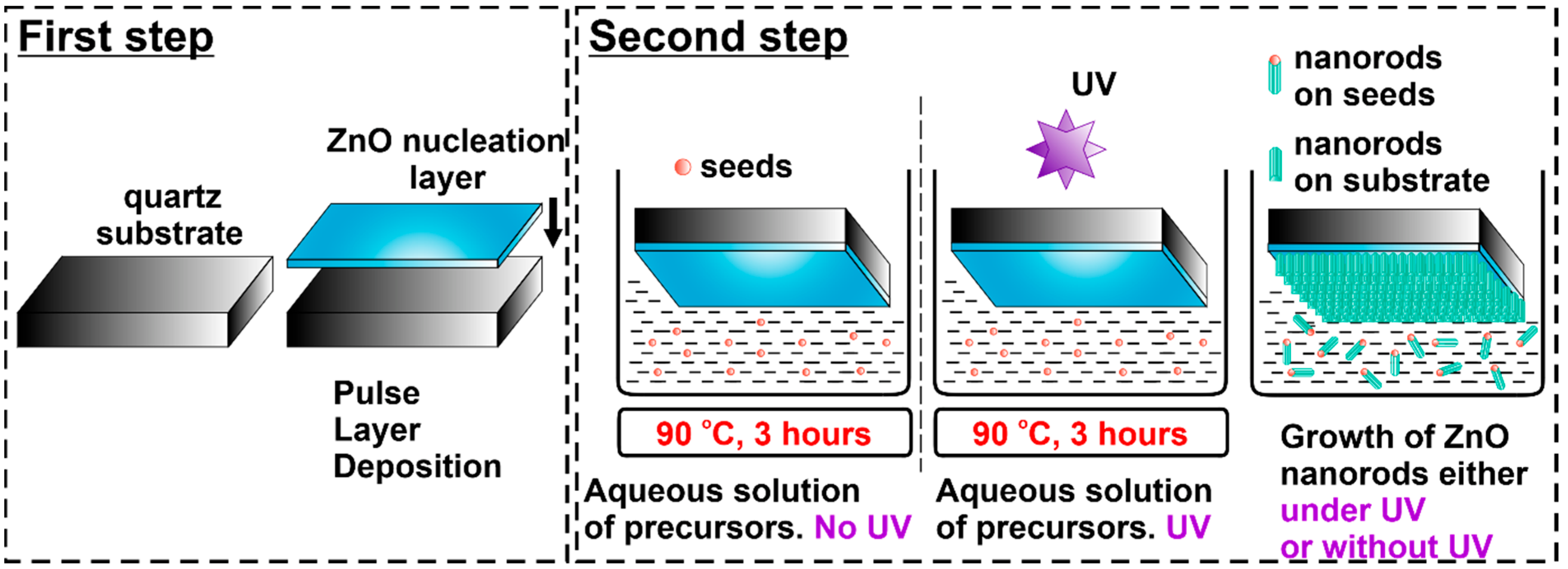
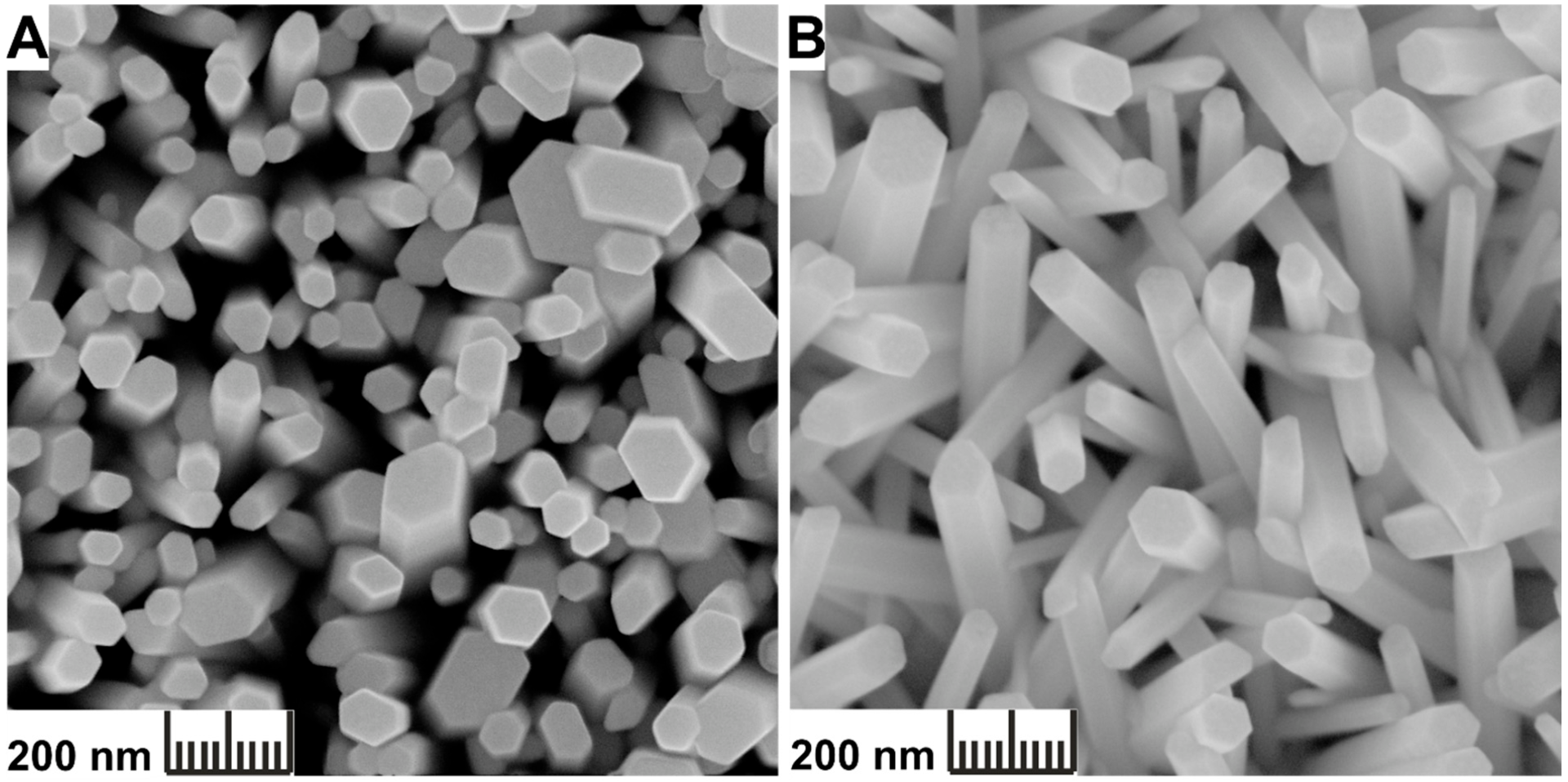
3.1. Structural Analysis

To check whether the studied materials were indeed ZnO, the XRD technique was applied. The patterns of the ZnO:Er FS samples are shown in Figure 2A.
According to the PDF-2 database (record #00-005-0664), all the ZnO:Er FS samples (with 0.05 and 0.25% Er doping level, grown under constant UV irradiation or not) are pure-phase Wurtzite ZnO.
The XRD patterns of the ZnO:Er GS samples are shown in Figure 2B. The pronounced peak at 34.5° corresponds to the (002) reflection, the crystallographic c direction (PDF-2 database, record #00-005-0664). The tiniest (103) and (004) peaks were also observed. No other peaks were detected, indicating that only the Wurtzite ZnO phase was present in all the samples (with 0.05 and 0.25% Er doping level, grown under constant UV irradiation or not). The SEM images in Figure 3 show the morphology of the ZnO:Er GS samples grown under UV irradiation and without it. ZnO:Er(0.25%) GS SEM images were used.
In the case of the ZnO:Er(0.25%) GS grown without UV, the distribution of the single nanorod size in the 40–200 nm range is observed, even though the approximately 40–60 nm thick nanorods dominate (Figure 3A). The nanorods are aligned almost perpendicular to the substrate. In the ZnO:Er(0.25%) GS grown under UV, all the single nanorod thicknesses appear in the range of 50–100 nm without pronounced domination of the rods with the chosen size. One can see that the rods, in general, are not perfectly perpendicular to the substrate. Note that the thickness of the polycrystalline film of ZnO nanorods was approximately the same (~800 nm) in the samples grown under UV or without it. All of this led to the conclusion that the UV irradiation influences growth rate and contributes to the homogenization of the nanorod thickness distribution, as discussed in detail in [60] for the undoped ZnO nanorods.

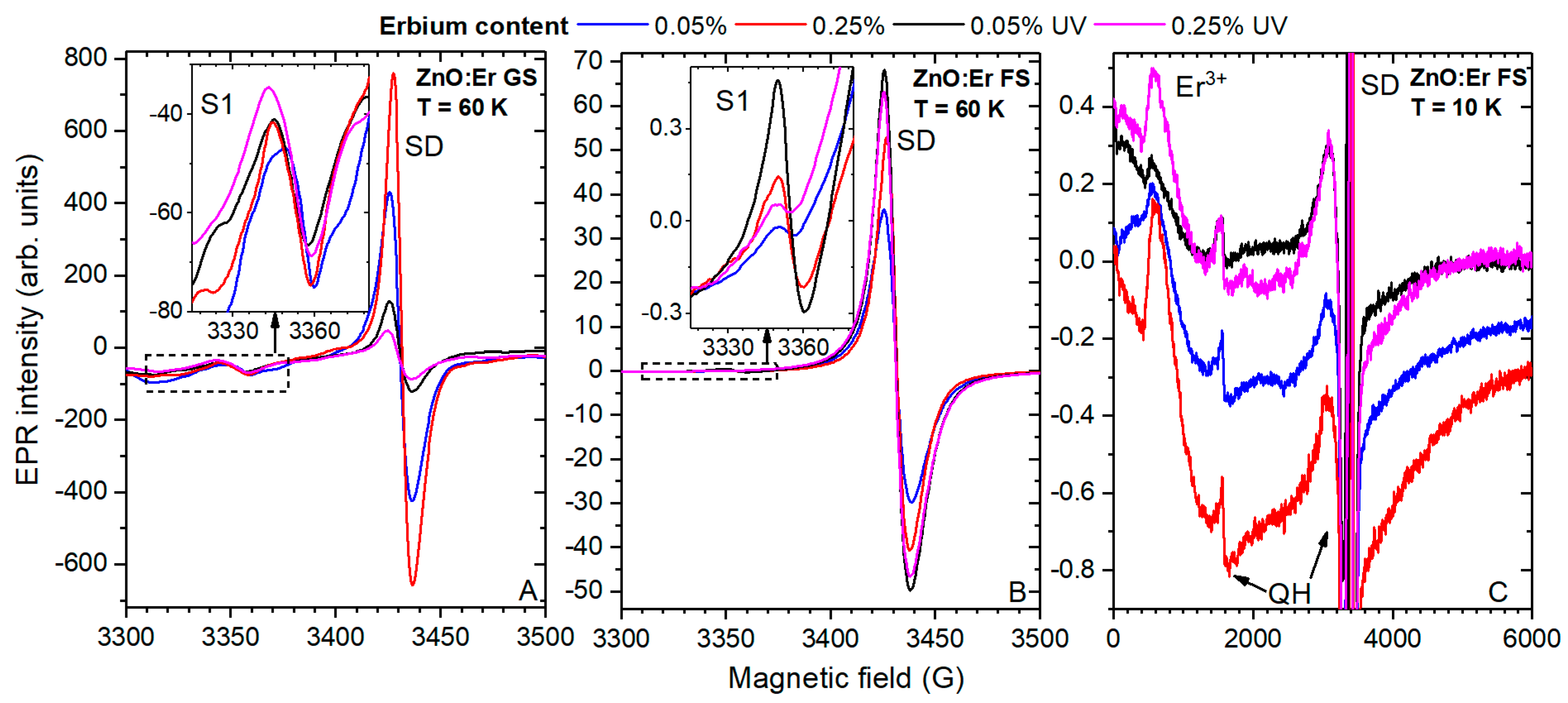
3.2. Paramagnetic States by EPR

To study the effect of UV irradiation on intrinsic defect states and Er incorporation into the ZnO:Er FS(GS) samples, EPR was used. The corresponding spectra measured in the ZnO:Er(0.05, 0.25%) GS grown without and under UV are shown in Figure 4A. They are, in general, composed of two signals, SD at the resonance magnetic field of 3430 G (corresponding to the g factor g = 1.954 at X-band; see Section 2.3 above) and S1 at the resonance magnetic field of 3348 G (corresponding to the g factor g = 1.9997 at X-band; see Experimental Section and the inset in Figure 4A). The intensity of the SD signal depended on the Er doping level as well as on the UV irradiation applied during the growth of the nanorods.
The SD signal originates from shallow donors with a complex structure, Zn+ + D, where D = Al, Ga, H, and Zn+ may also be interstitial [18,19,20,21,22,23,24,25,26] (see also Introduction). Relatively recently, it has also been related to the zinc interstitial (Zni), Zni+ + D, in the Er-doped ZnO [75]. Therefore, the SD signal, at least partly, has presently been related to the Zni+ + D as well. Its intensity is about 1.5 times lower in the ZnO:Er(0.05%) GS as compared to the ZnO:Er(0.25%) GS. Er3+ is a donor in ZnO, and therefore the Er doping affects the intrinsic charge distribution in the two-step process:
(i) Er2+ → Er3+ + e; (ii) Zni2+ + e → Zni+
This improves donor properties as well as the electron transport abilities due to the electron capture through the increased number of Zni+ + D. Growth under UV irradiation causes a drop in the SD signal intensity by about 4 times in the ZnO:Er(0.05, 0.25%) GS UV samples. However, oppositely, the ZnO:Er(0.05%) to ZnO:Er(0.25%) GS UV SD signals intensity ratio is 1.5. The observed peculiarities can be explained in the following way. UV irradiation during the samples’ growth should have the opposite effect of hole trapping compensating the donor properties:
Zn i + + h +   U V   Zn i 2 +
Hole trapping is more pronounced in the ZnO:Er(0.25%) GS UV as compared to the ZnO:Er(0.05%) GS UV sample the more Zni2+ was created (Equation (2)) or the more Zni+ were removed. The latter correlates very well with the larger amount of erbium in the ZnO host, considering that erbium is expected to be interstitial in ZnO as reported in [32,41,75]. It competes with Zn, and the number of Zni drops. In addition, ultrafast exciton emission deteriorates as well, as discussed in the next subsection. All of these changes are signs of lower conductivity, and therefore charge mobility and transport, the most critical parameters in chemical sensing, will be worsened as well [52,58,59,60].
The intensity of the SD signal is about 1.2 times larger in the ZnO:Er(0.25%) FS as compared to the ZnO:Er(0.05%) FS sample. This is almost the same tendency as that discussed above for the ZnO:Er(0.05, 0.25%) GS samples. Therefore, the same charge transfer mechanism (Equation (1)) is expected to exist in this case. Oppositely, the SD signal increases by about 1.5 times in the ZnO:Er(0.05%) FS UV as compared to the ZnO:Er(0.25%) FS UV. At the same time, the SD signal increases by about 1.2 times in the ZnO:Er(0.25%) FS UV as compared to the ZnO:Er(0.25%) FS. Most probably, electron trapping is occurring at the Zn2+ in the ZnO:Er FS under constant UV irradiation applied during the samples’ growth: Zni2+ + e  U V Zni+. This improves the donor properties of the Zni+ as well as the electron transport abilities. Interestingly, the intensity of the SD signals in the ZnO:Er(0.05, 025%) FS UV samples is about the same (Figure 4B). The amount of Zni2+ states available for the electron capture should thus be limited by the ZnO host (it is a well-known phenomenon that interstitial defects stretch the crystal lattice). Therefore, the larger the Er content, the smaller the number of places available for the Zni2+ in the ZnO host.
The difference between the ZnO:Er FS and GS grown under UV irradiation should originate from the method of the irradiation “delivery” to the samples. In the case of the GS samples, UV comes directly through the quartz glass substrate to the ZnO nanorods (Figure 1). Oppositely, in the case of the FS samples, the UV irradiation must go through the ZnO GS nanorods and is strongly absorbed, leading to a kind of photovoltaic effect releasing electrons into the solution. These electrons then reach only the ZnO FS rods in the solution close to the ZnO GS nanorods (Figure 1); otherwise, they will be compensated. Another possible mechanism is reactive oxygen species (ROS, O2) creation in the place where the ZnO GS nanorods come into contact with the water solution. ROS can then interact with the ZnO FS rods in the solution leading to the same effect as if the electrons from ZnO GS directly interacted with the ZnO FS rod.
Based on the consideration above for the deposited samples, chemical sensing should be improved in the ZnO:Er(0.05, 0.25%) FS UV samples. It is worth noting that the influence of the Er doping on the shallow donor states is discussed in detail in previous studies on free-standing ZnO:Er nanorods [32,41].
The S1 signal was about one order of magnitude weaker than the SD one, and its intensity remained unchanged upon Er doping and/or irradiation during growth (Figure 4A). Together, these two discrepancies between the SD and S1 signals indicate the different origins of these signals. The S1 signal can be expected to be produced by conduction electrons as this signal at the g factor of g = 1.9988–1.9990 was observed in silicon and was referred to as being produced by conduction electrons [41,76,77]. The fact that the S1 signal remains unchanged under different conditions of growth and Er doping levels indicates almost the same surface properties, especially considering the core-shell model [30] and very low Er incorporation, as further confirmed.
Again, the S1 signal (attributed to the conduction electrons above) has been measured in the ZnO:Er FS samples as well. It is, in general, about two orders of magnitude weaker there as compared to the ZnO:Er GS samples (Figure 4B). This is in good agreement with the size of the ZnO nanorods in the case of the deposited and free-standing ones—the surface-to-volume ratio is larger in the GS as compared to FS. Therefore, since the EPR signal is directly proportional to the number of spins, the number of conduction electrons is expected to be much larger on the surface of the deposited nanorods. The S1 signal intensity is about three times larger in the ZnO:Er(0.25%) FS as compared to the ZnO:Er(0.05%) FS. In contrast, the S1 signal intensity is about three times larger in the ZnO:Er(0.05%) FS UV as compared to the ZnO:Er(0.25%) FS UV. As a consequence, the more Er, the better the surface properties, especially with UV irradiation applied during the ZnO:Er FS rod growth. The conduction electrons are compensated, probably, by the Er3+ + e → Er2+ mechanism leading to the break in the Er-ZnO bonding and further detaching of Er from the ZnO host. This is confirmed by direct measurements of the Er3+ signal discussed below.
The Er3+ signal originating from Er embedded into the ZnO host as interstitial, as discussed in [32,41], is shown in Figure 4C for the ZnO:Er(0.05, 0.25%) FS samples. It follows the trend of the Er doping level, but it is about two to three times weaker in the ZnO:Er(0.05, 0.25%) FS UV samples as compared to the samples grown without UV irradiation. Probably, UV irradiation partly breaks the weak bonding that appears when Er embeds into the host as an interstitial [32,41], thus preventing its stabilization there. As a result, the Er3+ EPR signal dropped in the samples grown under UV. Note that EPR intensity is directly proportional to the concentration of paramagnetic particles [78].
The Er3+ signal originating from Er embedded into the ZnO host as an interstitial [32,41] has never been observed in the ZnO:Er GS samples, either grown under UV irradiation or without it. This points to the significant segregation of Er in this case due to different conditions of growth as will be discussed in detail in a study published elsewhere. However, as mentioned above, erbium influences the properties of the GS nanorods, and therefore its presence in the ZnO lattice can still be expected.

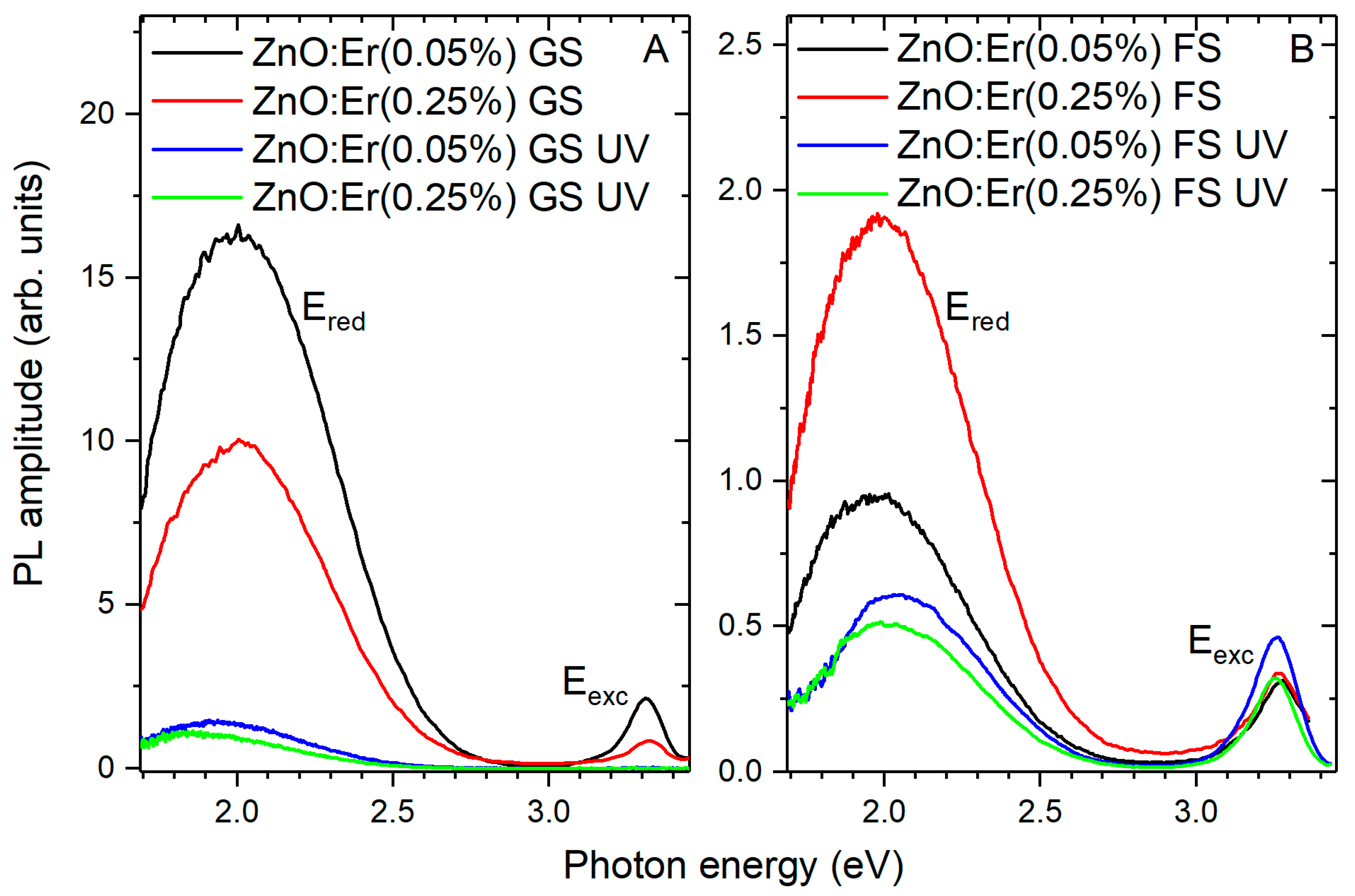
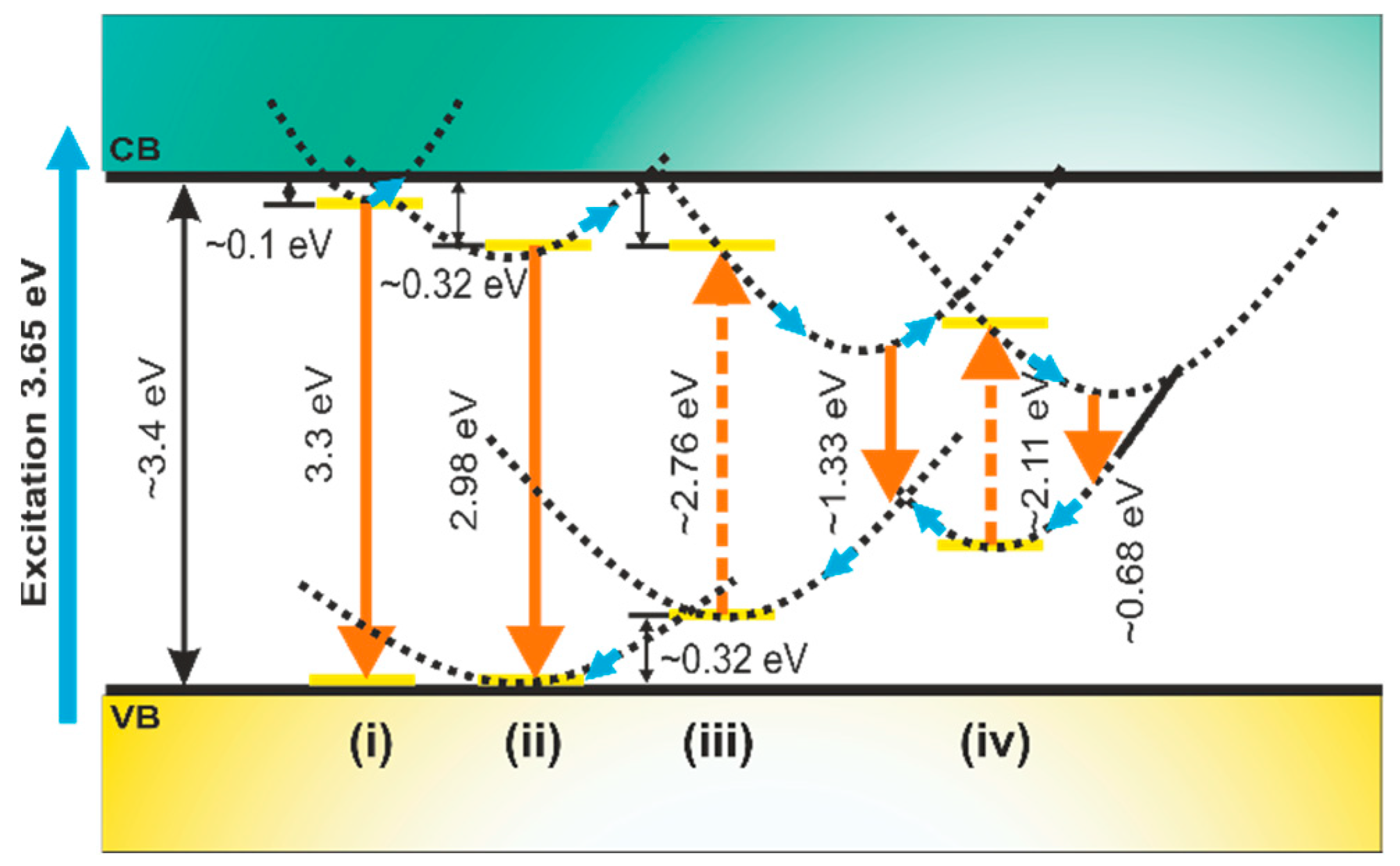
3.3. Photoluminescence Properties

The PL spectra measured in the ZnO:Er GS samples grown under UV and without UV are shown in Figure 5A. There were two emission bands observed: red band, Ered (peaking at about 2 eV), and Eexc (peaking at about 3.3 eV). The first one is known to be composed of the two contributions originating from neutral zinc vacancies, VZn0 and VZn0 + D (D is some defect nearby) as reported in a previous study [32]. Note that, in general, VZn2−,−,0,+,2+ are possible. None of them emits light in the visible region. The red band is about 1.5 times weaker in the ZnO:Er(0.25%) GS as compared to the ZnO:Er(0.05%) GS. This is in good agreement with the increased SD signal (see Figure 4A and the discussion above). The following charge compensation mechanism can be proposed:
(i) Er2+ → Er3+ + e; (ii) VZn0 + (2)e → VZn−(2−),
which is complementary to the mechanism in Equation (1).
Growth under constant UV irradiation led to a decreased red band in the ZnO:Er(0.05%) GS UV by approximately one order of magnitude. It decreased by about 5 times in the ZnO:Er(0.25%) GS UV. The most probable processes responsible for these phenomena are the following: Since the amount of erbium was significantly decreased as discussed above: (i) Zni+ + h+  U V Zni2+ or in an alternative representation Zni+  U V Zni2+ + e; (ii) VZn0 + (2)e → VZn−(2−). This correlates very well with Equation (2). Eexc band peaking at about 3.3 eV, which was attributed to excitons based on previous studies [32,41,79]. This was observed only in the PL spectra of the ZnO:Er(0.05, 0.25%) GS samples. It is about three times weaker in the ZnO:Er(0.25%) GS as compared to the ZnO:Er(0.05%) GS. This correlates well with the increased SD signal (Figure 4A) and decreased Ered (Figure 5A), i.e., the number of Zni+ is larger in the ZnO:Er(0.25%) GS as compared to the ZnO:Er(0.05%) GS. This excludes some electrons potentially participating in the exciton emission. As a result, the exciton emission becomes weaker. It is shown schematically in Figure 6. The PL excitation exceeds the bandgap. All the possible energy levels in the bandgap thus become ionized. After this, there are several possible ways that charge/energy transfer occurs. The electrons in the exciton excited states can be radiatively relaxed to the ground state (mechanism (i) in Figure 6) or the electron is passed to the excited state of Zni+. Again, there are two possibilities—to radiatively return to the corresponding ground state (mechanism (ii) in Figure 6) or to be relaxed to the excited state of VZn [22]. Note that, typically, Zni+ can hardly be detected at room temperature (this is described in detail in [41]). It was not presently observed either (see Figure 5). Therefore, most probably, the electron appears in the excited state of VZn and then can be radiatively returned to the corresponding ground state (mechanism (iii) in Figure 6) where emission appears at 1.33 eV [22], the region beyond the abilities of the detector used, or again it can be passed to VZn0 creating the excited state of VZn2− (mechanism (iv) in Figure 6). This situation is known for the Eu2+-F+ center dimer in Y3Al5O12 [80].
Appearing at the excited state of the VZn2− and the VZn again, an electron has two ways either to radiatively recombine to produce the emission at 0.68 eV [22], which is not reachable by the detectors used, or to relax nonradiatively to the ground state of the VZn2−, then to VZn, and after that to Zni+ and the valence band. The whole way the excited electron wanders until nonradiative relaxation to the valence band is shown by the blue arrows in Figure 6. The mechanisms (iii) and (iv) cannot be excluded as well.
The Eexc band is almost totally missing in samples grown under constant UV irradiation. This correlates with the red band and the mechanism behind the changes in its intensity upon the growth under UV irradiation considering the electrons compensating the neutral zinc vacancy. The lack of these electrons contributes to the degradation of the exciton emission. This proves at least the partial incorporation of erbium into the ZnO host.
There were two emission bands observed in the PL spectra of the ZnO:Er(0.05, 0.25%) FS samples grown under UV irradiation and without it (Figure 5B): red band, Ered (peaking at about 2 eV), composed of the two contributions originating from neutral zinc vacancies VZn0 and VZn0 + D (D is some defect nearby), as discussed in [32,41,79], and exciton emission Eexc (peaking at about 3.25 eV). The trends for the red and exciton band intensities as functions of the Er doping level are about the same as those described previously for the ZnO:Er free-standing nanorods [32,41,79]. However, the growth under UV irradiation had a similar but much less pronounced effect on the red band as in the case of the ZnO:Er(0.05, 0.25%) GS UV samples discussed above (degrading). The exciton band remained unchanged in the PL spectrum of the ZnO:Er(0.25%) FS UV as compared to the ZnO:Er(0.25%) FS. In contrast, the exciton emission was improved by about 1.2 times in the ZnO:Er(0.05%) FS UV as compared to the ZnO:Er(0.05%) FS samples. This can be explained by the strong scattering and dispersion of the UV light in the solution, and therefore only a very small effect was observed in the ZnO:Er FS UV as compared to the ZnO:Er GS UV for the red band and the opposite in the case of the exciton band (see Experimental Section for the growth details). This was also discussed in detail in the subsection above. Note also that the luminescence properties, in general, are about one order of magnitude stronger in the deposited nanorods. This also indicates better charge transport abilities (weaker charge trapping properties), which are necessary for the high performance of luminescence and scintillation as well as sensing abilities.

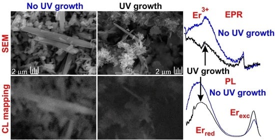
3.4. Morphology and Spatial Correlation of Luminescence and Elemental Composition

The CL spectra of the ZnO:Er(0.05, 0.25%) FS and ZnO:Er(0.05, 0.25%) FS UV samples are shown in Figure 7.
Since no PL exciton emission was observed in the deposited nanorods in the samples grown under UV irradiation (Figure 5), only the free-standing ones were further considered for the spatial correlation of exciton luminescence. To improve the signal, the samples were annealed in air at 350 °C as this has been proven to be a reliable method for the enhancement of the exciton and reduction in defect-related luminescence [32,41,79]. The red band (which shifted after the annealing to 1.85 eV as discussed in detail in [32,41,79]) remained almost unchanged in the ZnO:Er(0.05, 0.25%) FS and ZnO:Er(0.05%) FS UV but dropped by almost two times in the ZnO:Er(0.25%) FS UV. In general, this does not fully correlate with the PL measurements (Figure 5); however, this can be the result of higher power density in the case of CL as compared to PL. As a result, not all emission centers are activated in the case of PL. This is also confirmed by the observation of the specific forbidden Er3+ transitions (4F9/2 → 4I15/2, 4S3/2, 4H11/2 → 4I15/2) [75] indicated in Figure 7. Note that they were not observed in the PL spectra.
The exciton band (at about 3.15 eV) is typically observed to be redshifted by about 0.1 eV in CL as compared to PL, as mentioned in [75]. It has approximately the same intensity in the ZnO:Er(0.05, 0.25%) FS, while it is about fourfold smaller in the ZnO:Er(0.05, 0.25%) FS UV samples. This does not correlate well with the PL measurements (Figure 5B) due to the higher power density in the case of CL as compared to PL [82,83]. This can be the same reason for the redshifted CL as compared to PL, and therefore some exciton states become saturated and do not contribute to the spectrum [75].
The spatial correlation of the CL at 3.15 eV with the ZnO:Er FS and FS UV nanorods (SEM) and EDX mapping of the elements was measured as well and is shown in Figure 8.
The ZnO:Er(0.05, 0.25%) FS and ZnO:Er(0.05, 0.25%) FS UV samples are predominately 400 nm thick and 1–2 μm long rods. However, there are also much larger rods present: about 1 μm thick and over 6–8 μm long in the ZnO:Er(0.05, 0.25%) FS samples and about 0.5 μm thick and over 4–6 μm long in the ZnO:Er(0.05, 0.25%) FS UV samples. This can be seen in Figure 8A,F,K,P and led to the interpretation that UV irradiation applied during the sample growth leads to the downsizing of the free-standing rods. This indicates that the lower growth rate is probably due to the partial breaking of the bonds created during the growth, as discussed above for Er. By correlating one by one the CL and SEM for all the samples in the order of ZnO:Er(0.05%) FS (Figure 8A,B), ZnO:Er(0.05%) FS UV (Figure 8F,G), ZnO:Er(0.25%) FS (Figure 8K,L), and ZnO:Er(0.25%) FS UV (Figure 8P,Q), the brightness of the exciton emission follows the trend of the Eexc band intensity in Figure 7, i.e., the exciton emission of the samples grown under UV irradiation is less bright than that grown without UV irradiation. Moreover, the exciton emission was found to be more intense from large rods (about 1 μm thick and over 6–8 μm long), whereas smaller rods (400 nm thick and 1–2 μm long) emitted only faintly in all the ZnO:Er(0.05, 0.25%) FS and ZnO:Er(0.05, 0.25%) FS UV samples (Figure 8A,B,F,G,K,L,P,Q).
The samples were also characterized by EDX spectroscopy and mapping. For example, Zn distribution correlates perfectly well to the SEM images in the order of ZnO:Er(0.05%) FS (Figure 8A,C), ZnO:Er(0.05%) FS UV (Figure 8F,H), ZnO:Er(0.25%) FS (Figure 8K,M), and ZnO:Er(0.25, 0.25%) FS UV (Figure 8P,R). However, the EDX map of oxygen is less pronounced than that of zinc in the order of ZnO:Er(0.05%) FS (Figure 8A,D), ZnO:Er(0.05%) FS UV (Figure 8F,I), ZnO:Er(0.25%) FS (Figure 8K,N), and ZnO:Er(0.25, 0.25%) FS UV (Figure 8P,S). This can be partly explained by the much lower Z number of oxygen as compared to zinc. Note that a correlation between the lack of oxygen and CL intensity was observed. Considering the greatest mismatch between the Zn and O EDX mapping observed for the ZnO:Er(0.25%) FS sample (Figure 8K,N), the presence of some other processes, for example, the creation of oxygen vacancies, can be expected. Oxygen vacancy (VO) requires charge compensation, and the most natural compensation mechanism is zinc vacancy (VO2+ = VZn2−). The presence of zinc vacancies was proved in the subsection dedicated to photoluminescence above.
A slight correlation between Er EDX maps and SEM images can be found for the ZnO:Er(0.05%) FS (Figure 8A,E) and ZnO:Er(0.25%) FS (Figure 8K,O). No correlation was observed for the Er EDX maps and SEM images of the ZnO:Er(0.05%) FS UV (Figure 8F,J) and ZnO:Er(0.25%) FS UV (Figure 8P,T). This is in good agreement with the intensity of Er3+ EPR spectra (Figure 4C) directly proportional to the concentration of paramagnetic particles [78]—the amount of erbium is much smaller in samples grown under UV irradiation.
The exciton band was redshifted and strongly decreased in the CL spectra of the samples grown under UV irradiation, whereas in the PL spectra it remained almost unchanged under the same conditions (Figure 5 and Figure 7) and even slightly increased in the ZnO:Er(0.05%) FS UV (Figure 5). Therefore, one may conclude that the origin of the exciton luminescence is at least partly defect-related. Moreover, note that the different-sized nanorods were emitting in different ways, as discussed above (Figure 8B,G,L,Q). This is most probably connected with band-edge fluctuations in non-stochiometric regions of ZnO.

4. Conclusions

The main goal of this study was to investigate the atomistic aspects influencing the luminescence and transport abilities of Er-doped ZnO nanorods of different morphologies, grown under constant UV irradiation and without it. The study was thus focused on shallow donors, conduction electrons, zinc vacancies and excitons, and the source of free carriers activated under UV irradiation. Growth under constant UV irradiation has never been carried out before for erbium-doped ZnO deposited nanorods, and the free-standing nanorods grown under a kind of photovoltaic effect in the same solution as the deposited ones have never been obtained and studied. It was found that the number of donor states and conduction electrons is about one order of magnitude larger in the deposited nanorods as compared to the free-standing ones. Growth under constant UV irradiation caused a substantial decrease in the number of shallow donor states in the deposited nanorods (about fivefold). The effect is the opposite but less pronounced in the free-standing nanorods. This was explained by the different number of zinc vacancies as well as erbium incorporation. Note that the segregation of Er is high in the case of deposited nanorods. In addition, the UV irradiation applied during growth also resulted in a threefold decrease in the amount of erbium embedded into the ZnO host (free-standing nanorods) due to the breaking of the bonding.
Correlated experiments of EPR, PL, and CL + EDX + SEM suggested the origin of exciton luminescence to be at least partly defect-related, most probably due to band-edge fluctuations in non-stochiometric regions of ZnO.

Author Contributions

Conceptualization, M.B.; Methodology, N.N., L.L., R.K.S. and O.P.-G.; Formal analysis, M.B., K.R., L.L., F.H., V.B., K.D., R.K.S. and O.P.-G.; Investigation, M.B., K.R., N.N., F.H. and K.D.; Resources, V.B.; Data curation, M.B.; Writing—original draft, M.B.; Writing—review & editing, M.B., K.R., N.N., F.H. and V.B.; Visualization, K.R., N.N., L.L., F.H., V.B., K.D., R.K.S. and O.P.-G.; Supervision, M.B.; Project administration, M.B.; Funding acquisition, M.B. All authors have read and agreed to the published version of the manuscript.

Funding

This work was supported by the Czech Science Foundation, project No. 20-05497Y.

Institutional Review Board Statement

Not applicable.

Informed Consent Statement

Not applicable.

Data Availability Statement

Not applicable.

Acknowledgments

This work was supported by the Czech Science Foundation, project No. 20-05497Y. We are grateful to Zdenek Remeš for his contribution to the discussion.

Conflicts of Interest

The authors declare no conflict of interest.

References

  1. Awasthi, K. (Ed.) Nanostructured Zinc Oxide: Synthesis; Properties and Applications, 1st ed.; Elsevier: Cambridge, UK, 2021. [Google Scholar]
  2. Fedotov, A.; Pashkevich, A.; Fedotova, J.; Fedotov, A.; Kołtunowicz, T.; Zukowski, P.; Ronassi, A.; Fedotova, V.; Svito, I.; Budzyński, M. Electron transport and thermoelectric properties of ZnO ceramics doped with Fe. J. Alloys Compd. 2021, 854, 156169. [Google Scholar] [CrossRef]
  3. Pashkevich, A.; Fedotov, A.; Poddenezhny, E.; Bliznyuk, L.; Fedotova, J.; Basov, N.; Kharchanka, A.; Zukowski, P.; Koltunowicz, T.; Korolik, O.; et al. Structure, electric and thermoelectric properties of binary ZnO-based ceramics doped with Fe and Co. J. Alloys Compd. 2022, 895, 162621. [Google Scholar] [CrossRef]
  4. Selim, M.; El-Safty, S.; Abbas, M.; Shenashen, M. Facile design of graphene oxide-ZnO nanorod-based ternary nanocomposite as a superhydrophobic and corrosion-barrier coating. Colloids Surf. A Physicochem. Eng. Asp. 2021, 611, 125793. [Google Scholar] [CrossRef]
  5. Selim, M.; Shenashen, M.; Elmarakbi, A.; EL-Saeed, A.; Selim, M.; El-Safty, S. Sunflower oil-based hyperbranched alkyd/spherical ZnO nanocomposite modeling for mechanical and anticorrosive applications. RSC Adv. 2017, 7, 21796–21808. [Google Scholar] [CrossRef] [Green Version]
  6. Sánchez-López, A.; Perfecto-Avalos, Y.; Sanchez-Martinez, A.; Ceballos-Sanchez, O.; Sepulveda-Villegas, M.; Rincón-Enríquez, G.; Rodríguez-González, V.; Garcia-Varela, R.; Lozano, L.; Navarro-López, D.E.; et al. Influence of erbium doping on zinc oxide nanoparticles: Structural, optical and antimicrobial activity. Appl. Surf. Sci. 2022, 575, 151764. [Google Scholar] [CrossRef]
  7. Askar, A.; Selim, M.; El-Safty, S.; Hashem, A.; Selim, M.; Shenashen, M. Antimicrobial and immunomodulatory potential of nanoscale hierarchical one-dimensional zinc oxide and silicon carbide materials. Mater. Chem. Phys. 2021, 263, 124376. [Google Scholar] [CrossRef]
  8. Neykova, N.; Brož, A.; Remeš, Z.; Hruška, K.; Kalbáčová, M.; Kromka, A.; Vaněček, M. ZnO hedgehog-like structures for control cell cultivation. Appl. Surf. Sci. 2012, 258, 3485–3489. [Google Scholar] [CrossRef]
  9. Yang, C.; Zhan, S.; Li, Q.; Wu, Y.; Jia, X.; Li, C.; Liu, K.; Qu, S.; Wang, Z.; Wang, Z. Systematic investigation on stability influence factors for organic solar cells. Nano Energy 2022, 98, 107299. [Google Scholar] [CrossRef]
  10. Pezhooli, N.; Rahimi, J.; Hasti, F.; Maleki, A. Synthesis and evaluation of composite TiO2@ZnO quantum dots on hybrid nanostructure perovskite solar cell. Sci. Rep. 2022, 12, 9885. [Google Scholar] [CrossRef]
  11. Neykova, N.; Hruska, K.; Holovsky, J.; Remes, Z.; Vanecek, M. Arrays of ZnO nanocolumns for 3-dimensional very thin amorphous and microcrystalline silicon solar cells. Thin Solid Films 2013, 543, 110–113. [Google Scholar] [CrossRef]
  12. Laokae, D.; Phuruangrat, A.; Wannapop, S.; Dumrongrojthanath, P.; Thongtem, T.; Thongtem, S. Preparation, characterization and photocatalytic properties of Er-doped ZnO nanoparticles synthesized by combustion method. Int. J. Mater. Res. 2023, 114, 34–42. [Google Scholar] [CrossRef]
  13. Gomaa, H.; El-Safty, S.; Shenashen, M.; Kawada, S.; Yamaguchi, H.; Abdelmottaleb, M.; Cheira, M. Three-Dimensional, Vertical Platelets of ZnO Carriers for Selective Extraction of Cobalt Ions from Waste Printed Circuit Boards. ACS Sustain. Chem. Eng. 2018, 6, 13813–13825. [Google Scholar] [CrossRef]
  14. D’Agostino, D.; Di Giorgio, C.; Bobba, F.; Di Trolio, A.; Alippi, P.; Cucolo, A.; Bonapasta, A.A. Effects of cobalt substitution on ZnO surface reactivity and electronic structure. J. Mater. Chem. C 2019, 7, 8364–8373. [Google Scholar] [CrossRef]
  15. Olejnik, M.; Kersting, M.; Rosenkranz, N.; Loza, K.; Breisch, M.; Rostek, A.; Prymak, O.; Schürmeyer, L.; Westphal, G.; Köller, M.; et al. Cell-biological effects of zinc oxide spheres and rods from the nano- to the microscale at sub-toxic levels. Cell Biol. Toxicol. 2021, 37, 573–593. [Google Scholar] [CrossRef]
  16. Kapat, K.; Shubhra, Q.; Zhou, M.; Leeuwenburgh, S. Piezoelectric Nano-Biomaterials for Biomedicine and Tissue Regeneration. Adv. Funct. Mater. 2020, 30, 1909045. [Google Scholar] [CrossRef] [Green Version]
  17. Siebert, L.; Luna-Cerón, E.; García-Rivera, L.; Oh, J.; Jang, J.; Rosas-Gómez, D.; Pérez-Gómez, M.; Maschkowitz, G.; Fickenscher, H.; Oceguera-Cuevas, D.; et al. Light-Controlled Growth Factors Release on Tetrapodal ZnO-Incorporated 3D-Printed Hydrogels for Developing Smart Wound Scaffold. Adv. Funct. Mater. 2021, 31, 2007555. [Google Scholar] [CrossRef]
  18. Janotti, A.; Van de Walle, C. Native point defects in ZnO. Phys. Rev. B 2007, 76, 165202. [Google Scholar] [CrossRef]
  19. Janotti, A.; Van de Walle, C. Fundamentals of zinc oxide as a semiconductor. Rep. Prog. Phys. 2009, 72, 126501. [Google Scholar] [CrossRef] [Green Version]
  20. Morazzoni, F.; Scotti, R.; Volontè, S. Electron paramagnetic resonance investigation of paramagnetic point defects in ZnO and ZnO-supported ruthenium. J. Chem. Soc. Faraday Trans. 1990, 86, 1587–1591. [Google Scholar] [CrossRef]
  21. Van de Walle, C. Hydrogen as a Cause of Doping in Zinc Oxide. Phys. Rev. Lett. 2000, 85, 1012–1015. [Google Scholar] [CrossRef] [Green Version]
  22. Frodason, Y.; Johansen, K.; Bjørheim, T.; Svensson, B.; Alkauskas, A. Zn vacancy as a polaronic hole trap in ZnO. Phys. Rev. B 2017, 95, 094105. [Google Scholar] [CrossRef] [Green Version]
  23. Mackova, A.; Malinsky, P.; Pupikova, H.; Nekvindova, P.; Cajzl, J.; Svecova, B.; Oswald, J.; Wilhelm, R.; Kolitsch, A. A comparison of the structural changes and optical properties of LiNbO3, Al2O3 and ZnO after Er+ ion implantation. Nucl. Instrum. Methods Phys. Res. Sect. B Beam Interact. Mater. At. 2014, 331, 182–186. [Google Scholar] [CrossRef]
  24. Anjana, R.; Jayaraj, M.; Yadav, A.; Jha, S.; Bhattacharyya, D. Investigating the evolution of local structure around Er and Yb in ZnO:Er and ZnO:Er, Yb on annealing using X-ray absorption spectroscopy. J. Appl. Phys. 2018, 123, 153102. [Google Scholar] [CrossRef]
  25. Wang, J.; Zhou, M.; Hark, S.; Li, Q.; Tang, D.; Chu, M.; Chen, C. Local electronic structure and luminescence properties of Er doped ZnO nanowires. Appl. Phys. Lett. 2006, 89, 221917. [Google Scholar] [CrossRef]
  26. Honglin, L.; Yingbo, L.; Jinzhu, L.; Ke, Y. Experimental and first-principles studies of structural and optical properties of rare earth (RE = La, Er, Nd) doped ZnO. J. Alloys Compd. 2014, 617, 102–107. [Google Scholar] [CrossRef]
  27. Zhang, M.; Averseng, F.; Krafft, J.-M.; Borghetti, P.; Costentin, G.; Stankic, S. Controlled Formation of Native Defects in Ultrapure ZnO for the Assignment of Green Emissions to Oxygen Vacancies. J. Phys. Chem. C 2020, 124, 12696–12704. [Google Scholar] [CrossRef]
  28. Jakes, P.; Erdem, E. Finite size effects in ZnO nanoparticles: An electron paramagnetic resonance (EPR) analysis: Finite size effects in ZnO nanoparticles: An electron paramagnetic resonance (EPR) analysis. Phys. Status Solidi RRL 2011, 5, 56–58. [Google Scholar] [CrossRef]
  29. Kaftelen, H.; Ocakoglu, K.; Thomann, R.; Tu, S.; Weber, S.; Erdem, E. EPR and photoluminescence spectroscopy studies on the defect structure of ZnO nanocrystals. Phys. Rev. B 2012, 86, 014113. [Google Scholar] [CrossRef]
  30. Parashar, S.; Murty, B.; Repp, S.; Weber, S.; Erdem, E. Investigation of intrinsic defects in core-shell structured ZnO nanocrystals. J. Appl. Phys. 2012, 111, 113712. [Google Scholar] [CrossRef]
  31. Nadupalli, S.; Repp, S.; Weber, S.; Erdem, E. About defect phenomena in ZnO nanocrystals. Nanoscale 2021, 13, 9160–9171. [Google Scholar] [CrossRef]
  32. Buryi, M.; Remeš, Z.; Babin, V.; Artemenko, A.; Vaněček, V.; Dragounová, K.A.; Landová, L.; Kučerková, R.; Mičová, J. Transformation of free-standing ZnO nanorods upon Er doping. Appl. Surf. Sci. 2021, 562, 150217. [Google Scholar] [CrossRef]
  33. Buryi, M.; Remeš, Z.; Babin, V.; Novotný, M.; Vaněček, V.; Dragounová, K.A.; Mičová, J.; Landová, L.; Kučerková, R.; More-Chevalier, J.; et al. Influence of Mo doping on the luminescence properties and defect states in ZnO nanorods. Comparison with ZnO:Mo thin films. Appl. Surf. Sci. 2021, 555, 149679. [Google Scholar] [CrossRef]
  34. Erdem, E. Microwave power; temperature, atmospheric and light dependence of intrinsic defects in ZnO nanoparticles: A study of electron paramagnetic resonance (EPR) spectroscopy. J. Alloys Compd. 2014, 605, 34–44. [Google Scholar] [CrossRef]
  35. Yamazoe, N. New approaches for improving semiconductor gas sensors. Sens. Actuators B Chem. 1991, 5, 7–19. [Google Scholar] [CrossRef]
  36. Nikolic, M.; Milovanovic, V.; Vasiljevic, Z.; Stamenkovic, Z.; Sensors, S.G. Semiconductor gas sensors: Materials, technology, design, and application. Sensors 2020, 20, 6694. [Google Scholar] [CrossRef] [PubMed]
  37. Xu, F.; Ho, H.-P. Light-Activated Metal Oxide Gas Sensors: A Review. Micromachines 2017, 8, 333. [Google Scholar] [CrossRef] [Green Version]
  38. Peng, X.; Wang, Z.; Huang, P.; Chen, X.; Fu, X.; Dai, W. Comparative Study of Two Different TiO2 Film Sensors on Response to H2 under UV Light and Room Temperature. Sensors 2016, 16, 1249. [Google Scholar] [CrossRef] [PubMed] [Green Version]
  39. Fan, S.-W.; Srivastava, A.; Dravid, V. UV-activated room-temperature gas sensing mechanism of polycrystalline ZnO. Appl. Phys. Lett. 2009, 95, 142106. [Google Scholar] [CrossRef]
  40. Yu, K.; Shi, J.; Zhang, Z.; Liang, Y.; Liu, W. Synthesis, Characterization, and Photocatalysis of ZnO and Er-Doped ZnO. J. Nanomater. 2013, 2013, 372951. [Google Scholar] [CrossRef] [Green Version]
  41. Buryi, M.; Remeš, Z.; Babin, V.; Artemenko, A.; Chertopalov, S.; Mičová, J. Cold plasma treatment of ZnO:Er nano- and microrods: The effect on luminescence and defects creation. J. Alloys Compd. 2022, 895, 162671. [Google Scholar] [CrossRef]
  42. Lyons, J.; Varley, J.; Steiauf, D.; Janotti, A.; Van de Walle, C. First-principles characterization of native-defect-related optical transitions in ZnO. J. Appl. Phys. 2017, 122, 035704. [Google Scholar] [CrossRef]
  43. Stehr, J.; Chen, S.; Chen, W.; Cai, L.; Shen, S.; Buyanova, I. Effects of N implantation on defect formation in ZnO nanowires. Thin Solid Films 2019, 687, 137449. [Google Scholar] [CrossRef]
  44. Vlasenko, L. Magnetic Resonance Studies of Intrinsic Defects in ZnO: Oxygen Vacancy. Appl. Magn. Reson. 2010, 39, 103–111. [Google Scholar] [CrossRef]
  45. Vlasenko, L.; Watkins, G. Optical detection of electron paramagnetic resonance for intrinsic defects produced in ZnO by 2.5-MeV electron irradiation in situ at 4.2 K. Phys. Rev. B 2005, 72, 035203. [Google Scholar] [CrossRef]
  46. Gurylev, V.; Perng, T. Defect engineering of ZnO: Review on oxygen and zinc vacancies. J. Eur. Ceram. Soc. 2021, 41, 4977–4996. [Google Scholar] [CrossRef]
  47. Villafuerte, J.; Donatini, F.; Kioseoglou, J.; Sarigiannidou, E.; Chaix-Pluchery, O.; Pernot, J.; Consonni, V. Zinc Vacancy–Hydrogen Complexes as Major Defects in ZnO Nanowires Grown by Chemical Bath Deposition. J. Phys. Chem. C 2020, 124, 16652–16662. [Google Scholar] [CrossRef]
  48. Sun, Y.-F.; Liu, S.-B.; Meng, F.-L.; Liu, J.-Y.; Jin, Z.; Kong, L.-T.; Liu, J.-H. Metal Oxide Nanostructures and Their Gas Sensing Properties: A Review. Sensors 2012, 12, 2610–2631. [Google Scholar] [CrossRef] [Green Version]
  49. Moseley, P. Progress in the development of semiconducting metal oxide gas sensors: A review. Meas. Sci. Technol. 2017, 28, 082001. [Google Scholar] [CrossRef]
  50. Korotcenkov, G. Metal oxides for solid-state gas sensors: What determines our choice? Mater. Sci. Eng. B 2007, 139, 1–23. [Google Scholar] [CrossRef]
  51. Dey, A. Semiconductor metal oxide gas sensors: A review. Mater. Sci. Eng. B 2018, 229, 206–217. [Google Scholar] [CrossRef]
  52. Neykova, N.; Stuchlik, J.; Hruska, K.; Poruba, A.; Remes, Z.; Pop-Georgievski, O. Study of the surface properties of ZnO nanocolumns used for thin-film solar cells. Beilstein J. Nanotechnol. 2017, 8, 446–451. [Google Scholar] [CrossRef] [PubMed] [Green Version]
  53. Greene, L.; Law, M.; Tan, D.; Montano, M.; Goldberger, J.; Somorjai, G.; Yang, P. General Route to Vertical ZnO Nanowire Arrays Using Textured ZnO Seeds. Nano Lett. 2005, 5, 1231–1236. [Google Scholar] [CrossRef] [PubMed]
  54. Baruah, S.; Dutta, J. Hydrothermal growth of ZnO nanostructures. Sci. Technol. Adv. Mater. 2009, 10, 013001. [Google Scholar] [CrossRef]
  55. Kumar, V.; Gupta, R.; Bansal, A. Hydrothermal Growth of ZnO Nanorods for Use in Dye-Sensitized Solar Cells. ACS Appl. Nano Mater. 2021, 4, 6212–6222. [Google Scholar] [CrossRef]
  56. Demes, T.; Ternon, C.; Morisot, F.; Riassetto, D.; Legallais, M.; Roussel, H.; Langlet, M. Mechanisms involved in the hydrothermal growth of ultra-thin and high aspect ratio ZnO nanowires. Appl. Surf. Sci. 2017, 410, 423–431. [Google Scholar] [CrossRef]
  57. Buryi, M.; Remeš, Z.; Babin, V.; Chertopalov, S.; Děcká, K.; Dominec, F.; Mičová, J.; Neykova, N. Free-Standing ZnO:Mo Nanorods Exposed to Hydrogen or Oxygen Plasma: Influence on the Intrinsic and Extrinsic Defect States. Materials 2022, 15, 2261. [Google Scholar] [CrossRef] [PubMed]
  58. Buryi, M.; Babin, V.; Chang, Y.-Y.; Remeš, Z.; Mičová, J.; Šimek, D. Influence of precursor age on defect states in ZnO nanorods. Appl. Surf. Sci. 2020, 525, 146448. [Google Scholar] [CrossRef]
  59. Davydova, M.; Laposa, A.; Smarhak, J.; Kromka, A.; Neykova, N.; Nahlik, J.; Kroutil, J.; Drahokoupil, J.; Voves, J. Gas-sensing behaviour of ZnO/diamond nanostructures. Beilstein J. Nanotechnol. 2018, 9, 22–29. [Google Scholar] [CrossRef] [Green Version]
  60. Neykova, N.; Chang, Y.-Y.; Buryi, M.; Davydova, M.; Kucerkova, R.; Simek, D.; Remes, Z.; Pop-Georgievski, O. Study of ZnO nanorods grown under UV irradiation. Appl. Surf. Sci. 2019, 472, 105–111. [Google Scholar] [CrossRef]
  61. Achehboune, M.; Khenfouch, M.; Boukhoubza, I.; Derkaoui, I.; Leontie, L.; Carlescu, A.; Mothudi, B.; Zorkani, I.; Jorio, A. Optimization of the luminescence and structural properties of Er-doped ZnO nanostructures: Effect of dopant concentration and excitation wavelength. J. Lumin. 2022, 246, 118843. [Google Scholar] [CrossRef]
  62. Li, Q.; Liu, X.; Gu, M.; Hu, Y.; Li, F.; Liu, S.; Wu, Q.; Sun, Z.; Zhang, J.; Huang, S.; et al. Development of ZnO-based nanorod arrays as scintillator layer for ultrafast and high-spatial-resolution X-ray imaging system. Opt. Express 2018, 26, 31290. [Google Scholar] [CrossRef] [PubMed]
  63. Li, Q.; Yang, D.; Hao, S.; An, R.; Yuan, R.; Yang, Y.; Yang, X.; Huang, M.; Zhang, Z.; Liu, X.; et al. Development of the ZnO:Ga microrods—Epoxy composite as a scintillation screen for ultrafast X-ray detection. Opt. Mater. 2020, 102, 109805. [Google Scholar] [CrossRef]
  64. Liao, J.; Wang, M.; Lin, F.; Han, Z.; Fu, B.; Tu, D.; Chen, X.; Qiu, B.; Wen, H.-R. Thermally boosted upconversion and downshifting luminescence in Sc2(MoO4)3:Yb/Er with two-dimensional negative thermal expansion. Nat. Commun. 2022, 13, 2090. [Google Scholar] [CrossRef]
  65. Wang, H.; Xu, Y.; Pang, T.; Chen, B.; Xin, F.; Xing, M.; Tian, M.; Fu, Y.; Luo, X.; Tian, Y. Engineering Er3+-sensitized nanocrystals to enhance NIR II-responsive upconversion luminescence. Nanoscale 2022, 14, 962–968. [Google Scholar] [CrossRef]
  66. Huang, H.; Yuan, M.; Hu, S.; Zhong, Y.; Cui, W.; Guo, C.; Song, C.; Zhao, G.; Han, K. Nanosecond kinetics of multiphoton upconversion in an optically trapped single microcrystal. J. Mater. Chem. C 2022, 10, 9208–9215. [Google Scholar] [CrossRef]
  67. Elfeky, S.; Reda, S. MOF/Up-converting combination for photovoltaic application. J. Electroanal. Chem. 2021, 895, 115485. [Google Scholar] [CrossRef]
  68. Hu, J.; Yin, C.; Xu, S.; Cheng, M.; Wei, T.; Liu, Q.; Li, W.; Ling, Y.; Zhang, Y.; Liu, B. Enhanced room temperature NO2 sensing performance based on N-doped carbon nanosheets@ZnO nanoplates by morphology transition and white light illumination. Appl. Surf. Sci. 2022, 599, 153980. [Google Scholar] [CrossRef]
  69. Photaram, W.; Liangruksa, M.; Aiempanakit, M.; Suwanchawalit, C.; Wisitsoraat, A.; Sukunta, J.; Laksee, S.; Siriwong, C. Design and fabrication of zinc oxide-graphene nanocomposite for gas sensing applications. Appl. Surf. Sci. 2022, 595, 153510. [Google Scholar] [CrossRef]
  70. Zhang, M.; Zhang, H.; Li, L.; Tuokedaerhan, K.; Jia, Z. Er-enhanced humidity sensing performance in black ZnO-based sensor. J. Alloys Compd. 2018, 744, 364–369. [Google Scholar] [CrossRef]
  71. D’Arienzo, M.; Redaelli, M.; Di Credico, B.; Polizzi, S.; Scotti, R.; Morazzoni, F. New insights into the sensing mechanism of shape controlled ZnO particles. RSC Adv. 2016, 6, 52987–52997. [Google Scholar] [CrossRef]
  72. Chang, Y.-Y.; Remes, Z.; Micova, J. Mass production of hydrogenated ZnO nanorods. In Proceedings of the NANOCON 2019—Conference Proceedings, Brno, Czech Republic, 16–18 October 2020; pp. 221–225. [Google Scholar] [CrossRef]
  73. Chang, Y.-Y.; Stuchlík, J.; Neykova, N.; Souček, J.; Remeš, Z. Optical properties of the plasma hydrogenated ZnO thin films. J. Electr. Eng. 2017, 68, 70–73. [Google Scholar] [CrossRef] [Green Version]
  74. Mooney, J.; Kambhampati, P. Get the Basics Right: Jacobian Conversion of Wavelength and Energy Scales for Quantitative Analysis of Emission Spectra. J. Phys. Chem. Lett. 2013, 4, 3316–3318. [Google Scholar] [CrossRef]
  75. Buryi, M.; Neykova, N.; Ridzoňová, K.; Remeš, Z.; Děcká, K.; Hájek, F.; Artemenko, A.; Mičová, J.; Landová, L.; Jakubec, I. Peculiarities of erbium incorporation into ZnO microrods at high doping level leading to upconversion and the morphology change. Influence on excitonic as well as shallow donor states. Appl. Surf. Sci. 2023, 611, 155651. [Google Scholar] [CrossRef]
  76. Buryi, M.; Babin, V.; Remeš, Z.; Mičová, J. Charge trapping processes in hydrothermally grown Er-doped ZnO. Radiat. Meas. 2022, 150, 106700. [Google Scholar] [CrossRef]
  77. Klyui, N.; Bratus, V.; Temchenko, V.; Lozinskii, V.; Yukhymchuk, V.; Han, W.; Liu, B. EPR and Raman study of silicon layers obtained by gas detonation spraying. Mater. Sci. Semicond. Process. 2017, 71, 232–239. [Google Scholar] [CrossRef]
  78. Feher, G. Electron Spin Resonance Experiments on Donors in Silicon. I. Electronic Structure of Donors by the Electron Nuclear Double Resonance Technique. Phys. Rev. 1959, 114, 1219–1244. [Google Scholar] [CrossRef]
  79. Abragam, A.; Bleaney, B. Electron Paramagnetic Resonance of Transition Ions; Oxford University Press: Oxford, UK, 2012. [Google Scholar]
  80. Buryi, M.; Havlák, L.; Jarý, V.; Bárta, J.; Laguta, V.; Beitlerová, A.; Li, J.; Chen, X.; Yuan, Y.; Liu, Q.; et al. Specific absorption in Y3Al5O12:Eu ceramics and the role of stable Eu2+ in energy transfer processes. J. Mater. Chem. C 2020, 8, 8823–8839. [Google Scholar] [CrossRef]
  81. Shimada, R.; Urban, B.; Sharma, M.; Singh, A.; Avrutin, V.; Morkoç, H.; Neogi, A. Energy transfer in ZnO-anthracene hybrid structure. Opt. Mater. Express 2012, 2, 526. [Google Scholar] [CrossRef]
  82. Buryi, M.; Babin, V.; Hubáček, T.; Jarý, V.; Hájek, F.; Kuldová, K.; Artemenko, A.; Hospodková, A. The influence of Si on the properties of MOVPE grown GaN thin films: Optical and EPR study. Radiat. Meas. 2022, 157, 106842. [Google Scholar] [CrossRef]
  83. Vaněk, T.; Jarý, V.; Hubáček, T.; Hájek, F.; Kuldová, K.; Gedeonová, Z.; Babin, V.; Remeš, Z.; Buryi, M. Acceleration of the yellow band luminescence in GaN layers via Si and Ge doping. J. Alloys Compd. 2022, 914, 165255. [Google Scholar] [CrossRef]
Figure 1. Schematic processes of the ZnO:Er nanorod growth.
Chemosensors 11 00156 g001
Figure 2. (A) XRD patterns of ZnO:Er FS samples grown with and without external UV irradiation. The reflections are indicated by the vertical lines and (hkl) indices in accordance with the PDF-2 database (record #00-005-0664). (B) XRD patterns of the ZnO:Er GS samples grown with and without external UV irradiation. The dominating orientation (the direction of growth) is (002).
Chemosensors 11 00156 g002
Figure 3. (A) SEM image of the ZnO:Er(0.25%) GS sample grown without UV irradiation. (B) SEM image of the ZnO:Er(0.25%) GS sample grown under constant UV irradiation. The rest of the conditions of growth were the same.
Chemosensors 11 00156 g003
Figure 4. (A) EPR spectra measured in the ZnO:Er GS samples grown under UV irradiation and without it (the Er doping level as well the application of UV is indicated in the legend) at T = 60 K. (B) EPR spectra measured in the ZnO:Er FS samples grown under UV irradiation and without it (the Er doping level as well the application of UV is indicated in the legend) at T = 60 K. (C) EPR spectra measured in the ZnO:Er FS samples grown under UV irradiation and without it (the Er doping level as well the application of UV is indicated in the legend) at T = 10 K. The characteristic resonances are indicated by SD, S1, Er3+, and QH. The former three are meaningful and are discussed in the text while the latter one is the signal from the quartz sample holder and will be omitted in the discussion.
Chemosensors 11 00156 g004
Figure 5. (A) PL spectra measured in the ZnO:Er(0.05 and 0.25%) GS samples grown under UV and without it as indicated in the legend. (B) PL spectra measured in the ZnO:Er(0.05 and 0.25%) FS samples grown under UV and without it as indicated in the legend. Eexc and Ered indicate specific emission bands.
Chemosensors 11 00156 g005
Figure 6. The scheme of PL and relaxation of excited electron from exciton excited state (here all possible excitons are considered). Excitation of 3.65 eV is shown by vertical blue “up” arrow. The bandgap is shown by vertical double arrow with a value of about 3.4 eV [32]. Mechanism (i) exhibits exciton luminescence. Mechanism (ii) exhibits luminescence of Zni+ [81]. Mechanism (iii) exhibits luminescence of VZn [22]. Mechanism (iv) exhibits luminescence of VZn2− [22]. Orange solid “down” arrows stand for the emission whereas the orange dashed “up” arrows stand for the excitation. Small blue arrows indicate the path of nonradiative electron relaxation from the excited exciton state.
Chemosensors 11 00156 g006
Figure 7. CL spectra of the ZnO:Er(0.05, 0.25%) FS and ZnO:Er(0.05, 0.25%) FS UV at acceleration voltage U = 5 kV. The UV exciton band (~3.15 eV) and the red band (~1.85 eV) are marked Eexc and Ered, respectively. The specific forbidden Er3+ transitions (4F9/2 → 4I15/2, 4S3/2, 4H11/2 → 4I15/2) are indicated by vertical dashed lines.
Chemosensors 11 00156 g007
Figure 8. (A,F,K,P)—SE images; (B,G,L,Q)—CL images at 3.15 eV; (C,H,M,R)—EDX maps of Zn; (D,I,N,S)—EDX maps of (O); (E,J,O,T)—EDX maps of Er. (AE) panels belong to the ZnO:Er(0.05%) free-standing nanorods grown without UV. (FJ) panels belong to the ZnO:Er(0.05%) free-standing nanorods grown under constant UV. (KO) panels belong to the ZnO:Er(0.25%) free-standing nanorods grown without UV. (PT) panels belong to the ZnO:Er(0.25%) free-standing nanorods grown under constant UV. The elemental weight fraction is given in the panels.
Chemosensors 11 00156 g008
Disclaimer/Publisher’s Note: The statements, opinions and data contained in all publications are solely those of the individual author(s) and contributor(s) and not of MDPI and/or the editor(s). MDPI and/or the editor(s) disclaim responsibility for any injury to people or property resulting from any ideas, methods, instructions or products referred to in the content.

