The Influence of Structure Parameters on Nanoantennas’ Optical Response


1
Instituto Superior Técnico, 1049-001 Lisbon, Portugal
2
Instituto de Telecomunicações, 1049-001 Lisbon, Portugal
*
Author to whom correspondence should be addressed.
Chemosensors 2020, 8(2), 42; https://0-doi-org.brum.beds.ac.uk/10.3390/chemosensors8020042
Submission received: 21 May 2020
/
Revised: 10 June 2020
/
Accepted: 16 June 2020
/
Published: 19 June 2020
Abstract
:Currently, huge opportunities for the inclusion of new optical devices in our lives have been appearing. There are evident and irrefutable examples for nanoantenna applications. They can be used to improve already developed devices or even be used as the device. In both cases, they can be applied in diverse areas, such as medicine, environment, energy, defense, and communications. A square arrayed metallic nanoantenna composed of circular holes is studied by performing simulations using COMSOL Multiphysics. This article aims to study the influence of the nanoantenna’s metal, silver, gold, copper and aluminum, but also the optical response dependence on the nanoantenna’s periodicity, its thickness, the hole diameter, and the number of holes. It is evidenced that the optical response can be tuned using the structure parameters and by choosing an appropriate material. This tuning will allow developers to fulfil the specifications, since it is proven that the response peak can be deliberately shifted, amplified, or attenuated.
1. Introduction
Nanoantennas are nano-scaled metallic/plasmonic structures that support optical resonances and, consequently, the concentration and amplification of electromagnetic radiation [1,2,3]. When light is incident on the structure, surface plasmon polaritons can be generated, and their propagation is responsible for the aforementioned concentration and amplification [1,2,4,5,6]. A resonant peak is observable when analyzing the frequency response, varying the incident radiation wavelength/frequency, which is clear evidence of the propagation of those polaritons and the occurrence of the extraordinary optical transmission phenomenon [1,2,3,4,7]. This phenomenon was discovered by Ebbesen in 1998, who previously stated that this phenomenon would be very useful to develop new optical devices [3].
Huge progress in real-time measuring and in vitro sensors is ongoing, due to recent advances in nanotechnology [1,8,9,10,11,12,13,14,15,16]. However, computational methods, as well as the techniques for semiconductors and nanomaterials’ synthesis must be improved in order to allow the progress of nanotechnologies [1,8,9,10,11,12]. Several phenomena have been recently discovered, and they have been used as a basis to achieve different work principles. Sensors based on nanoantennas are a new category in this new paradigm that allow us to develop a miniaturized, standalone, and portable device [1,2,3,8]. The frequency response, mainly the resonant peak, will change regarding external physical or chemical phenomena that occur and interact with the nanostructure [1,7,8,16]. The variation of the structure optical properties, especially the complex dielectric function, with the medium variations, for example temperature, pressure, concentration, and materials, where the structure is immersed, results in spectral changes that can be useful to detect and monitor those variations of the medium [1].
On the other hand, these nanostructures can be also used to improve the capability to manipulate energy [1,5,6,17,18,19]. They can have an important role on the energy production sector, since they can be attached to or integrated in solar cells in order to improve their efficiency, once nanoantennas allow the amplification of electromagnetic radiation [1,17]. In other words, for the same amount of radiation that is incident on the cell, the output power can be higher, because the nanoantenna will amplify the incident radiation before it reaches the active area of the solar cell or even adjust the wavelength of the incident radiation, because the cells’ efficiency depends on the spectral region of the incident radiation. Every component or device that uses electromagnetic energy can be improved using nanoantennas. The devices used for optical communication are no exception, and nanoantennas have allowed us to create new filters or to improve the amplification sensibilities, using a nano-scale device [1,2,7,9,10,11,12,18,19].
This article aims to study these nanostructures’ optical responses, more specifically their parameter and material influence. The parameter influence, such as structure periodicity, hole diameter, structure thickness, or the number of holes, is an important study in order to develop a structure. Currently, the parameter influence on the output optical response is not as accurate as it should be, and consequently, there are no models that allow us to choose the best parameter values to fulfil a list of specifications [1,2,3,4,5,6,7,8,13,14,15,19]. This article aims to research and investigate these models. For four metals immersed in air and for different and independent parameter sweepings, a square arrayed nanoantenna composed of circular holes is tested.
2. Structure
The simulated structure was composed of a metallic array of circular holes immersed in a dielectric medium. The chosen structure was a square arrayed, because although there were already some theoretical studies for structures like this, they presented expressions based on the fact that the complex dielectric function did not vary. In this case, the work region was in the visible and near-infrared spectral regions, where this statement is not completely true [1,3]. Recent studies aimed to search for new models and formulations capable of predicting the dependence of the output optical response with the structure parameters [13,20,21,22,23].
This article presents a study of four different sweeps, as well as four different materials, considering the same simulation environment, inputs, and methods; for example: materials were modeled by the same type of fitting; the boundary conditions were not changed; the measurement conditions and the incident field were kept from the first simulation until the last one. Thus, it was possible to make conclusions about the sweeps’ influence and to compare them, aiming at the search for new models and formulations.
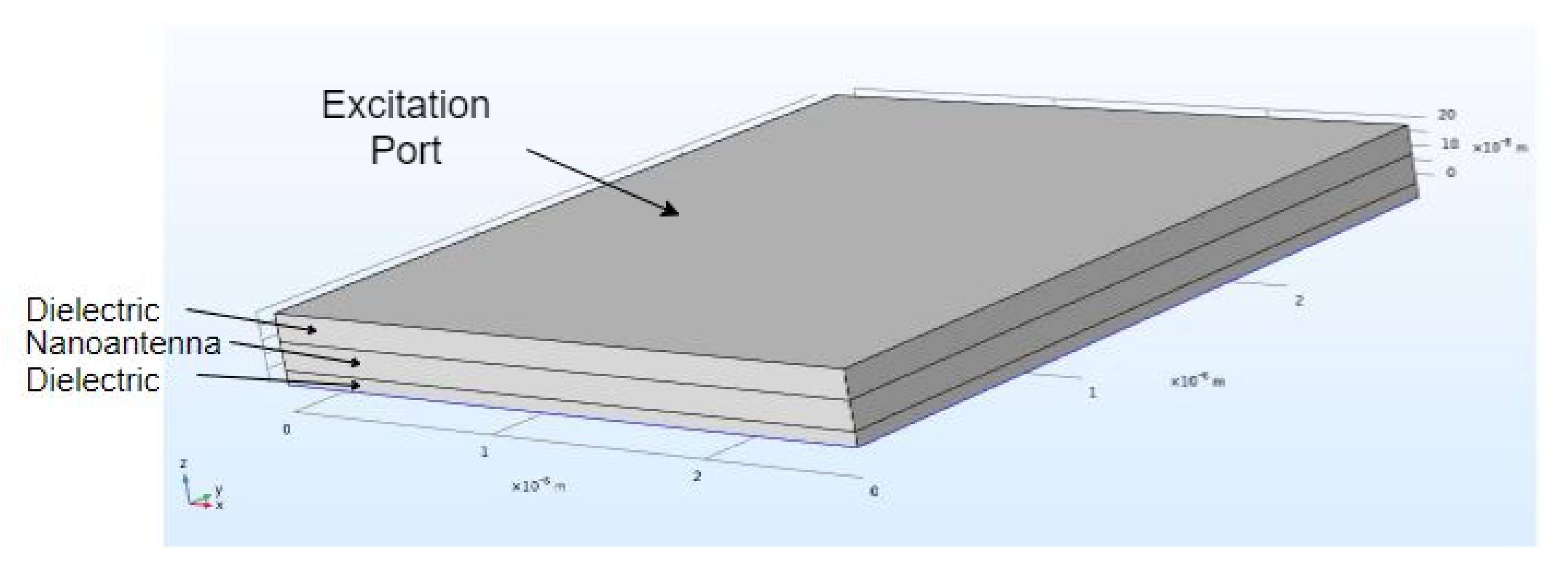
In Figure 1 is shown the simulation environment. An electric field was generated on the top boundary, having a norm of , and its propagation direction was in the opposite z axis direction, being perpendicular to the metal plane. Furthermore, this electric field was defined as and .
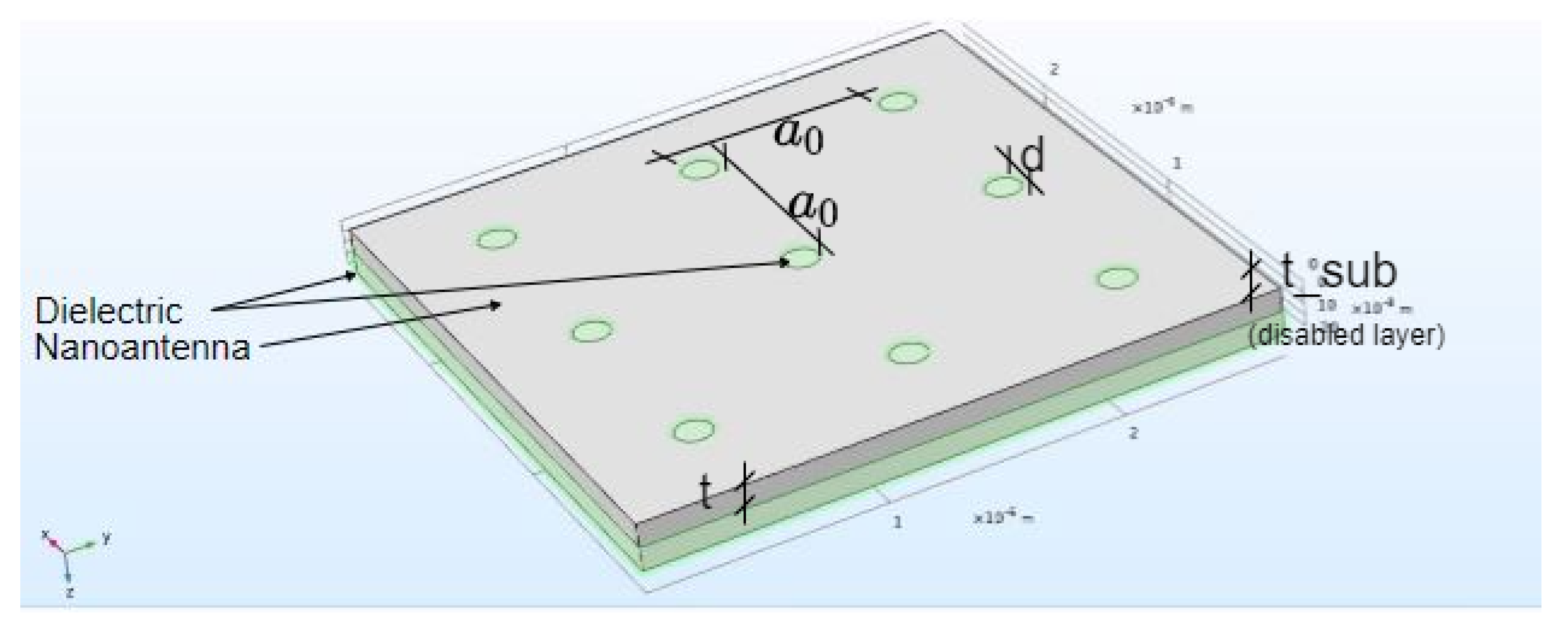
The metallic nanoantenna was a 3 × 3 array, forming a square lattice, where the circular holes were filled by the dielectric medium, as shown in Figure 2. In this figure is presented the same structure as presented in Figure 1; however, the structure was flipped, and the bottom dielectric layer was disabled. Thus, it was possible to illustrate the nanoantenna layer, as well as to define the sweep variables graphically. On the other hand, considering this figure, it was observable that the nanoantenna’s holes were filled by the dielectric medium. The nanoantenna had a hole periodicity of , a hole diameter of , and a thickness of . Moreover, the bottom dielectric layer, considering the structure presented in Figure 1, had a thickness of . Furthermore, the top dielectric medium had a thickness of ; however, when the nanoantenna thickness was swept, the distance between the electric field generation port, the top boundary, and the rear of the nanoantenna was the same, changing the dielectric thickness.
The main goal of this article is to measure the power intensity associated with the ratio between the generated electric field and the output one, , for each incident wavelength, regarding a range between and , using 250 equidistant points. Thus, boundary probes were placed on the structure, analyzing the maximum intensity field: one on the top external boundary, the input, where the electric field was generated, and the other on the bottom, in order to determine the amount of radiation detected in the structure’s output. Even more, all the external boundaries were defined as absorbing, such that there were no reflection.
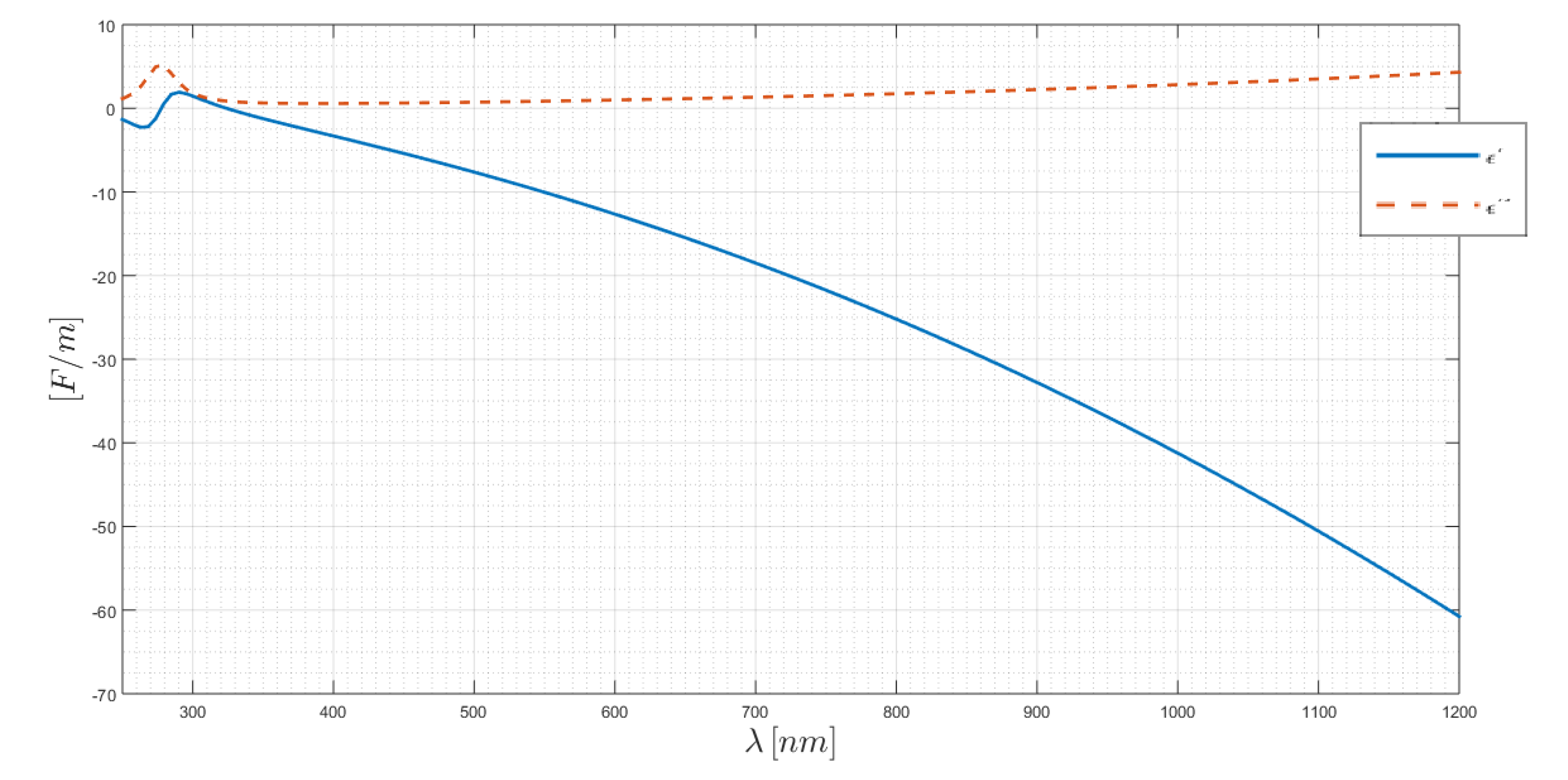
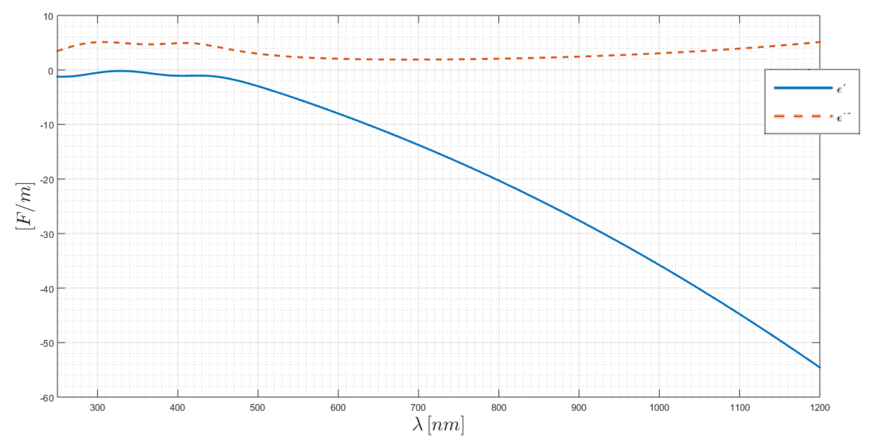
Air was considered as the dielectric medium, both for the top and bottom layers, including the holes, and the nanoantenna material was to be swept between four metals, silver, gold, copper, and aluminum. The air’s optical properties were modeled by Ciddor’s model, and the metals’ were simulated using Rakic’s Drude–Lorentz fitting [24]. The complex dielectric function for all the materials used is illustrated on Appendix A, considering the aforementioned models. Considering the figures from Appendix A, it is possible to follow the analysis.
Gold and copper have a small imaginary part of their dielectric function along the visible and near-infrared regions, but their interband maximum makes them not good materials to be used in this region, due to the proportional relation between Ohmic losses and the dielectric imaginary part [5,6,24]. Silver has a higher dielectric function imaginary part module, this maximum being the way to diminish its relative value and, consequently, the Ohmic losses [5,6,24]. The aluminum case was pretty different. Aluminum has an almost null dielectric function imaginary part until . After this, its value increases until a maximum located around , making this material the worst one to be used for red and near-infrared region applications and the best one to create gain for the entire visible region [5,6,24]. Gold and copper have very similar complex dielectric functions. They are used for red and near-infrared applications, since they have a transition between the Drude and the interband regimes around 530∼, i.e., 2 ∼2.3 eV [5,6,24]. On the other hand, silver can be better than copper or even gold, in a range between 600∼800 nm. Silver’s transition is bellow , or above 3 eV, making this material suitable to be used in the aforementioned range [5,6,24].
Another analysis that must be done of the materials is their chemical stability, in order to determine if their chemical formula and, consequently, their optical properties will remain the same. Silver and copper are known to be easily corroded materials, because oxides and sulfites can quickly be formed under ambient conditions [5,6]. Some passivation layers will be formed on aluminum, resulting in AlO [5,6]. Gold is an exception, and it is known as a material with an excellent chemical stability [5,6].
3. Parameter Influence
An analysis regarding the parameter sweep was performed using the previously defined air-metal-air structure.
The simulations results were divided per parameter sweep. The first parameter that was analyzed was the periodicity, . This sweep considered four different values: , , , and . Then, the hole diameter was analyzed; however, considering that the nanostructure periodicity remained constant and equal to , it was important to guarantee that the hole diameter would not be higher than the periodicity. As observed in Figure 2, if this happened, the structure would not be correctly defined. Thus, the hole diameter would vary between and , with a variation step equal to , leading to the extraction of four different results, without reaching half the periodicity. After that, the nanoantenna thickness would be swept, taking three different heights: , , and . The last parameter evaluated in this section is the number of holes. As the nanoantenna was a square array, six different arrays topologies would be tested, sweeping the number of lines and columns of the array: 3 × 3, 5 × 3, 7 × 3, 7 × 5, 5 × 5, and 7 × 7.
3.1. Periodicity Sweep
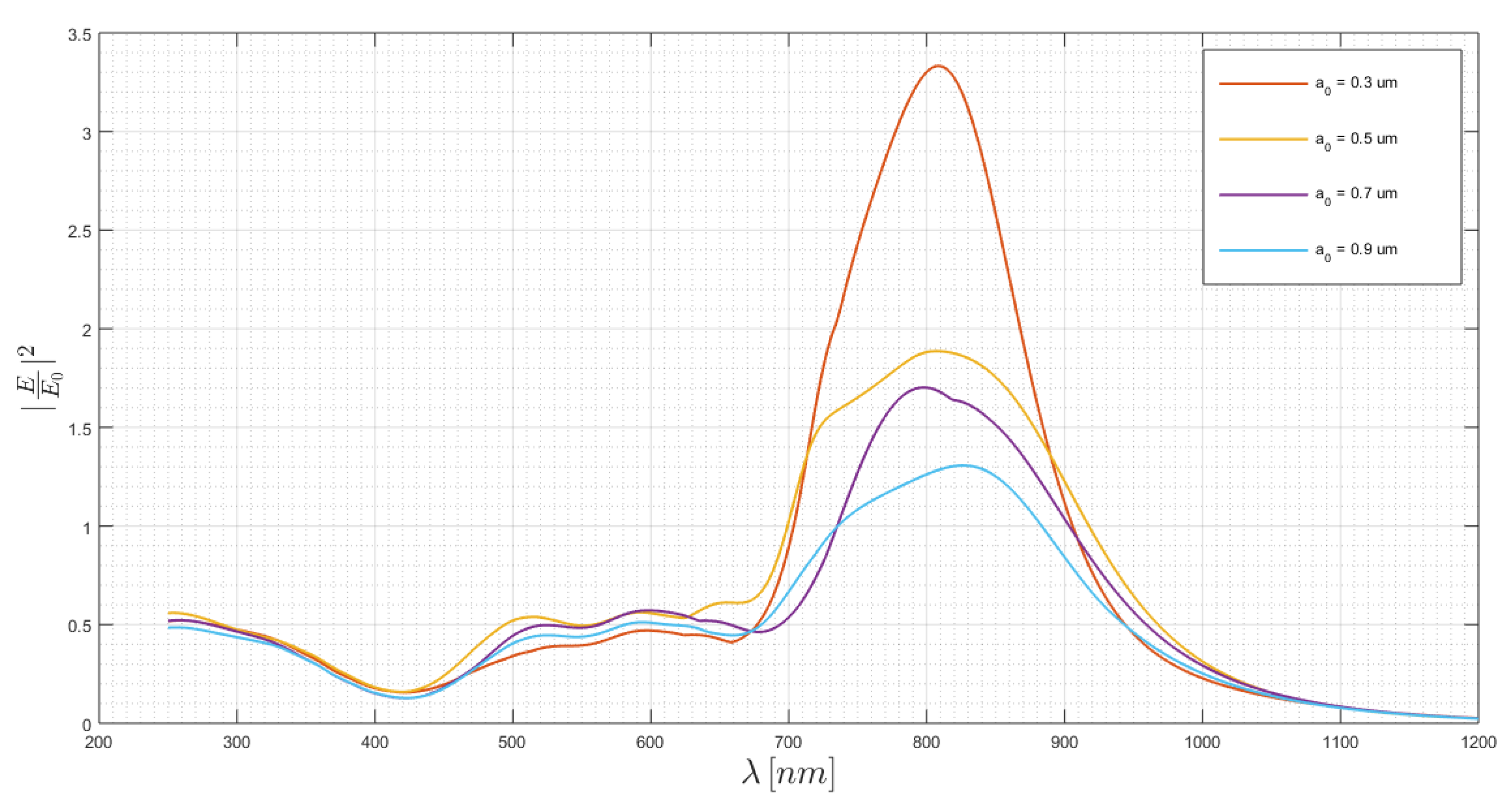
The first structure parameter that was swept was its periodicity. The first simulation results are presented in Figure 3, for a silver nanoantenna. It is possible to observe that despite this sweep, the maximum peak remained more or less at the same wavelengths.
On the other hand, it is possible to observe in Figure 3 that the peak intensity value seemed to decrease as the periodicity increased, having reached a maximum intensity peak for , where the output optical response had a gain of approximately 3.33, for an incident wavelength of . Even though, for the worst simulation case in terms of gain, a maximum ratio of 1.31 was achieved, for an incident wavelength of .
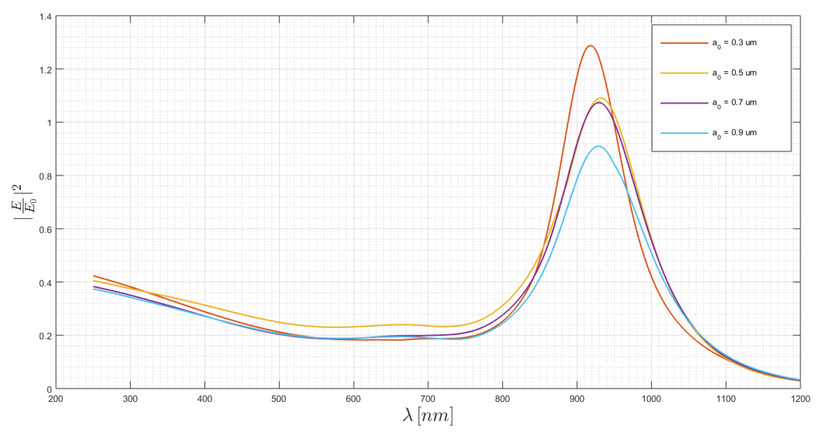
After this, a gold nanoantenna was simulated, and its results are illustrated in Figure 4. Here, it is possible to make the same conclusion as was made for the silver simulation set: when the periodicity increased, the peak intensity diminished, and the peak wavelength kept around the same value. In this case, for , the maximum optical gain was 1.28, for an incident wavelength of , and for , the lowest simulated maximum gain was 0.88, for an incident wavelength of . This case, , led already to a response without any gain region; however, the structure allowed the surface plasmon polaritons’ propagation, because it continued to reveal an output resonant spectrum.
Stepping forward to the next case, where a copper nanoantenna was tested, it was quite obvious that its response, presented in Figure 5, was similar to the gold one. However, none of the simulated tests had an optical response with gain. Further tests would allow us to understand that it was possible to have gain regions with a copper nanoantenna. On the other hand, the copper’s behavior seemed to be different from gold and silver, because there was not a linear dependence between the resonant peak and the periodicity. It was not true, for the copper case, that an increase of the structure periodicity led to lower intensity values and, consequently, to a lower maximum peak.
In this simulation set, the maximum achieved gain was around 0.78, which was reached both for , for an incident wavelength of , and for , for an incident wavelength of .
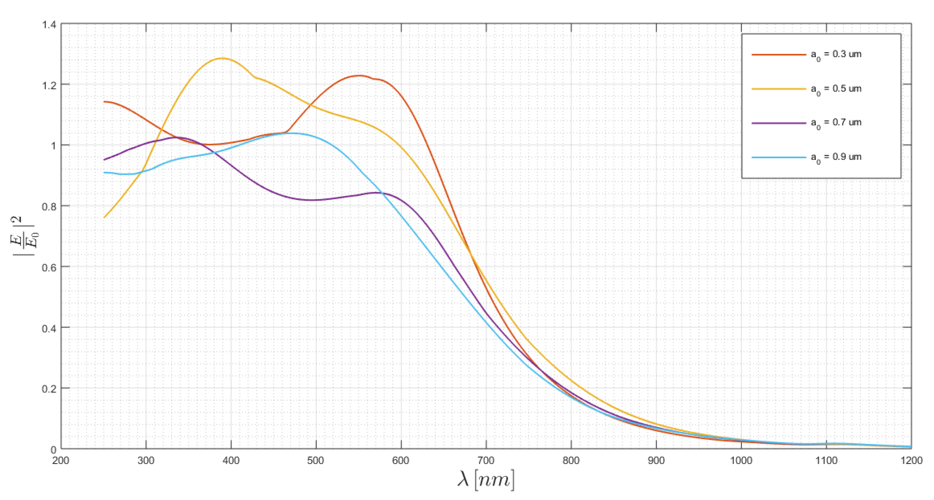
Last, but not the least, the simulation set performed for an aluminum nanoantenna is presented in Figure 6. As previously mentioned, due to a completely different complex dielectric function characteristic, the aluminum response would be different from the one analyzed for the other three materials. The aluminum optical response could be tuned in order to allow only the amplification of the visible and the huge attenuation of the other wavelengths. It was possible to observe that both and allowed having a gain region capable of amplifying almost all of the visible region, reaching maximum gain values around 1.23, for an incident wavelength of , and 1.29, for an incident wavelength of , respectively. Nonetheless, the aluminum optical response for seemed to have a larger gain region.
3.2. Hole Diameter Sweep
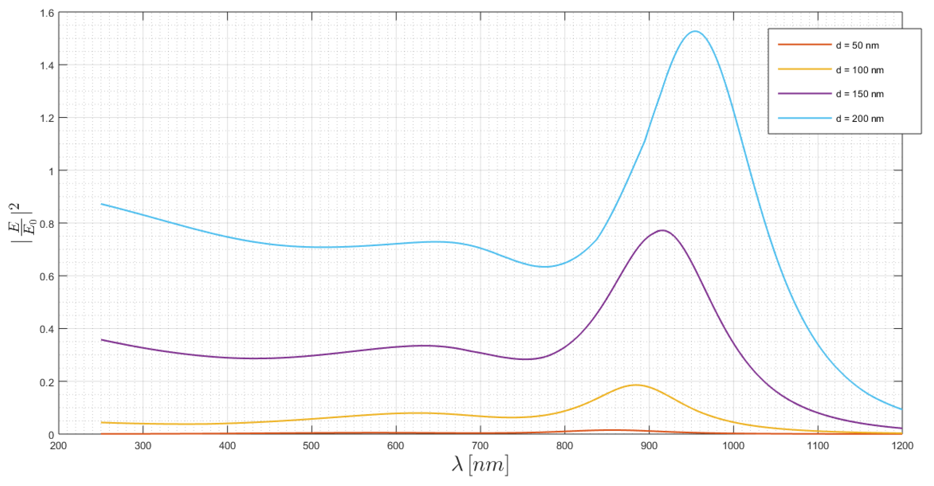
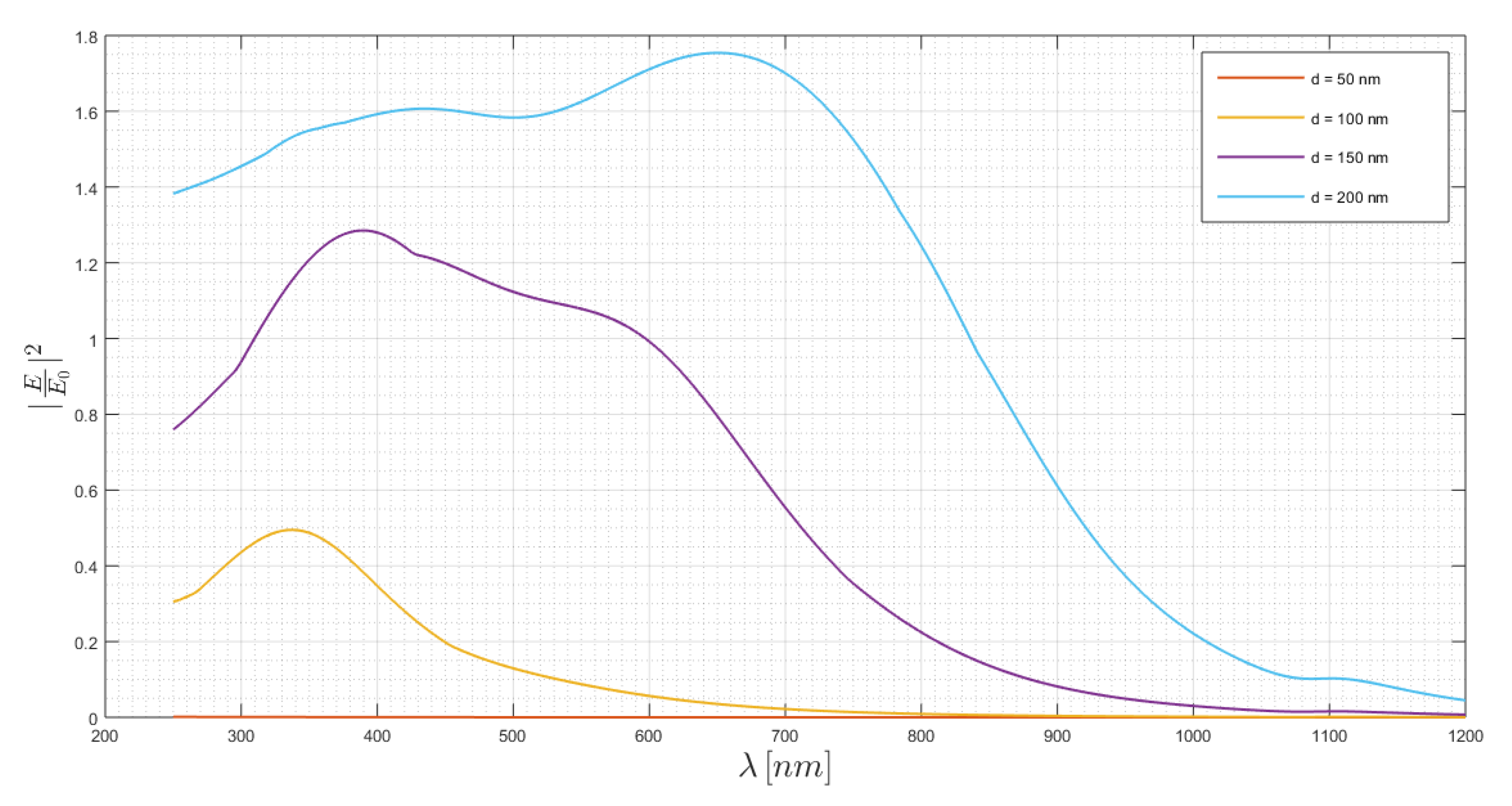
The next sweep considered the variation of the hole diameter from to , using a step variation of .
On the silver simulations set, illustrated in Figure 7, it was possible to verify that the maximum peak wavelength varied: as the hole diameter increased, red-shifts occurred. What was also quite impressive was that the minimum region, at wavelengths around , seemed not to change, so that when the hole diameter increased, the peak value increased as well; the peak wavelength was higher, and there was a transition region between the minimum and the maximum intensity peak that became larger and larger. This last conclusion led to the increasing of the gain region.
A gain of 2.77 was obtained for , for an incident wavelength of , and only a ratio of 0.19 was observed for , for an incident wavelength of . In this last situation, the optical response led to an extreme attenuation along all the range.
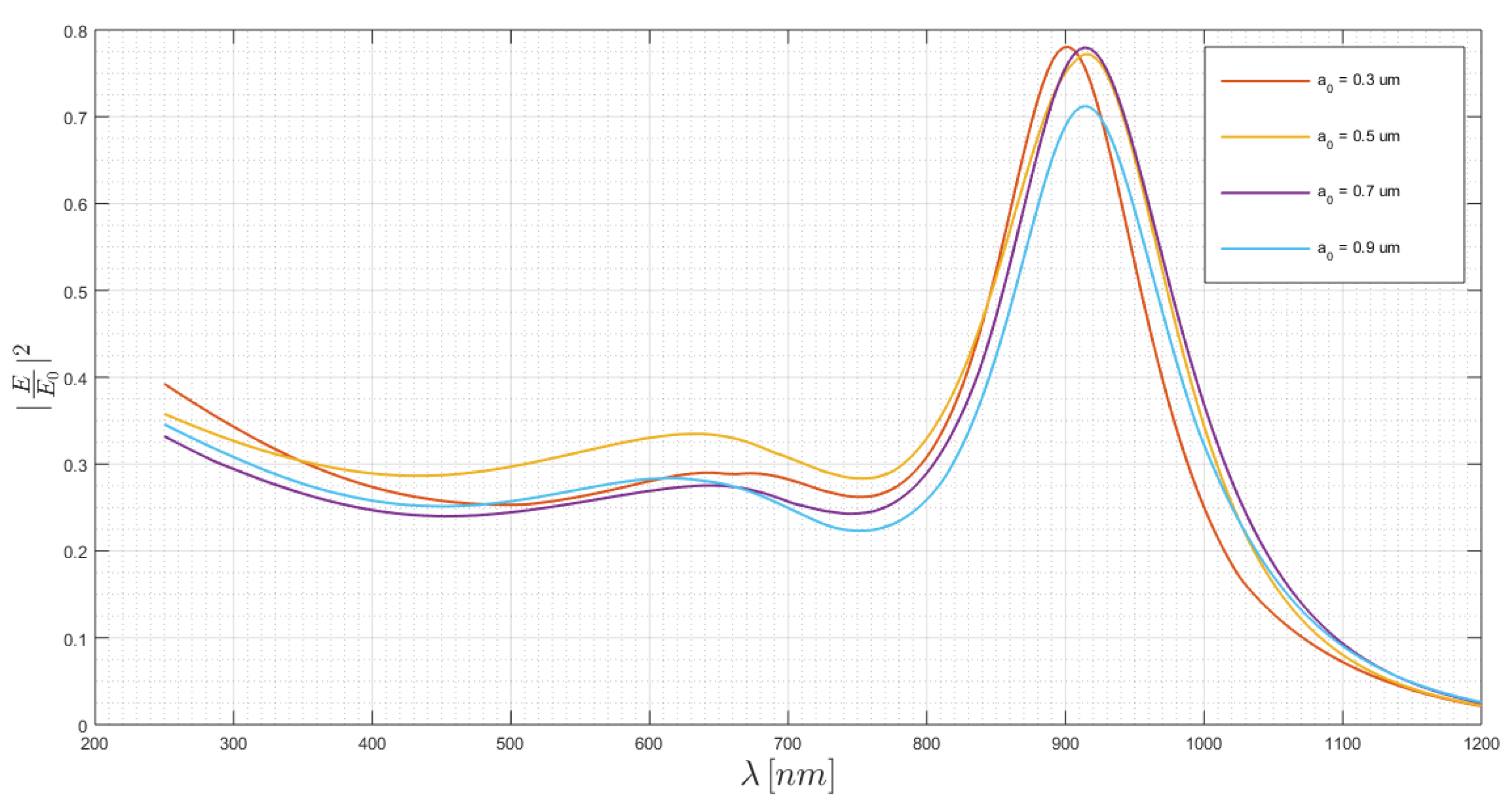
The same statements could be concluded when analyzing the gold and copper behavior, illustrated respectively in Figure 8 and Figure 9. Once again, it was obvious that both materials had similar behaviors when the hole diameter was swept. However, the copper optical response exhibited lower intensity peaks. For , the gold nanoantenna presented a maximum gain of 1.96, for an incident wavelength of , whereas copper had a response maximum of 1.53, for an incident wavelength of . On the other hand, it was observable that the copper response was more sensitive to the hole diameter sweep. For and , the output electromagnetic field was practically null, due to higher dispersion and Ohmic losses, in almost all the range for the copper nanoantennas, whereas, for the gold optical response, it was still possible to point out the resonant peak. On the other hand, as previously seen and discussed, for , the reference geometry, the gold nanoantenna presented a tiny and narrow gain region in comparison with no gain behavior obtained for copper. In addition, the peak shift was visible for both materials, as when the hole diameter increased, the red-shift occurred.
The aluminum optical response is presented in Figure 10, where it is also possible to verify that the bigger the hole diameter was, the higher the gain would be. Furthermore, the gain region became larger, expanding both spectral sides, i.e., despite it growing more to the red side, it also stretched to the violet side. This characteristic allowed us to tune the desired wavelength range to amplify. The highest gain, 1.75, was obtained for , for an incident wavelength of , and for , the output electromagnetic field was practically null for the simulated band.
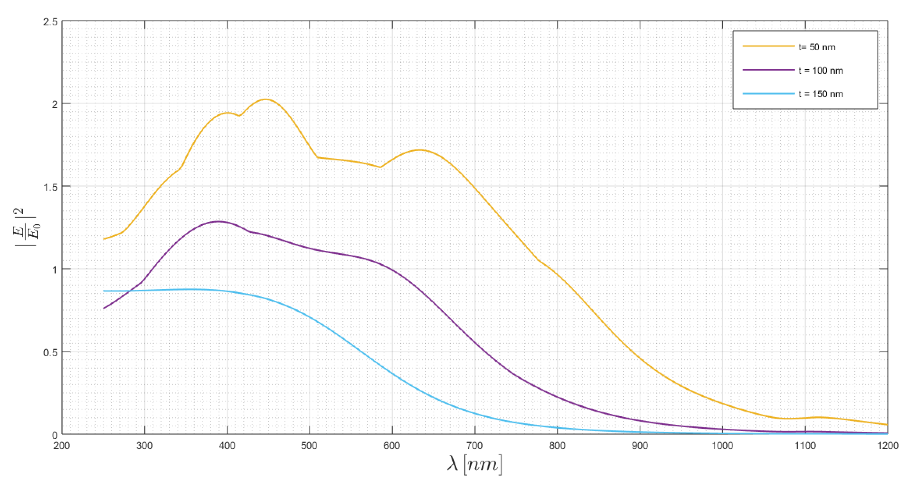
3.3. Nanoantenna Thickness Sweep
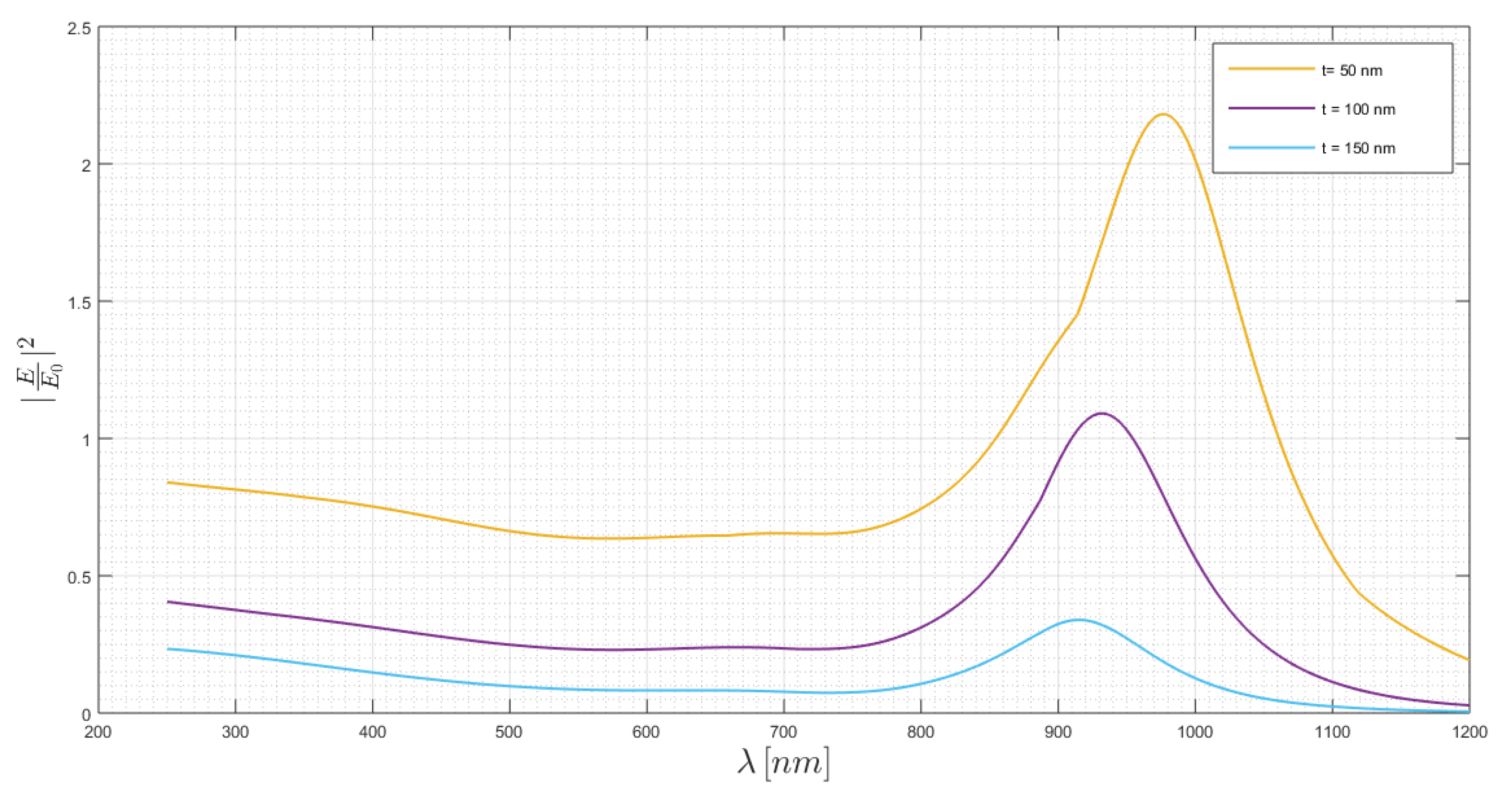
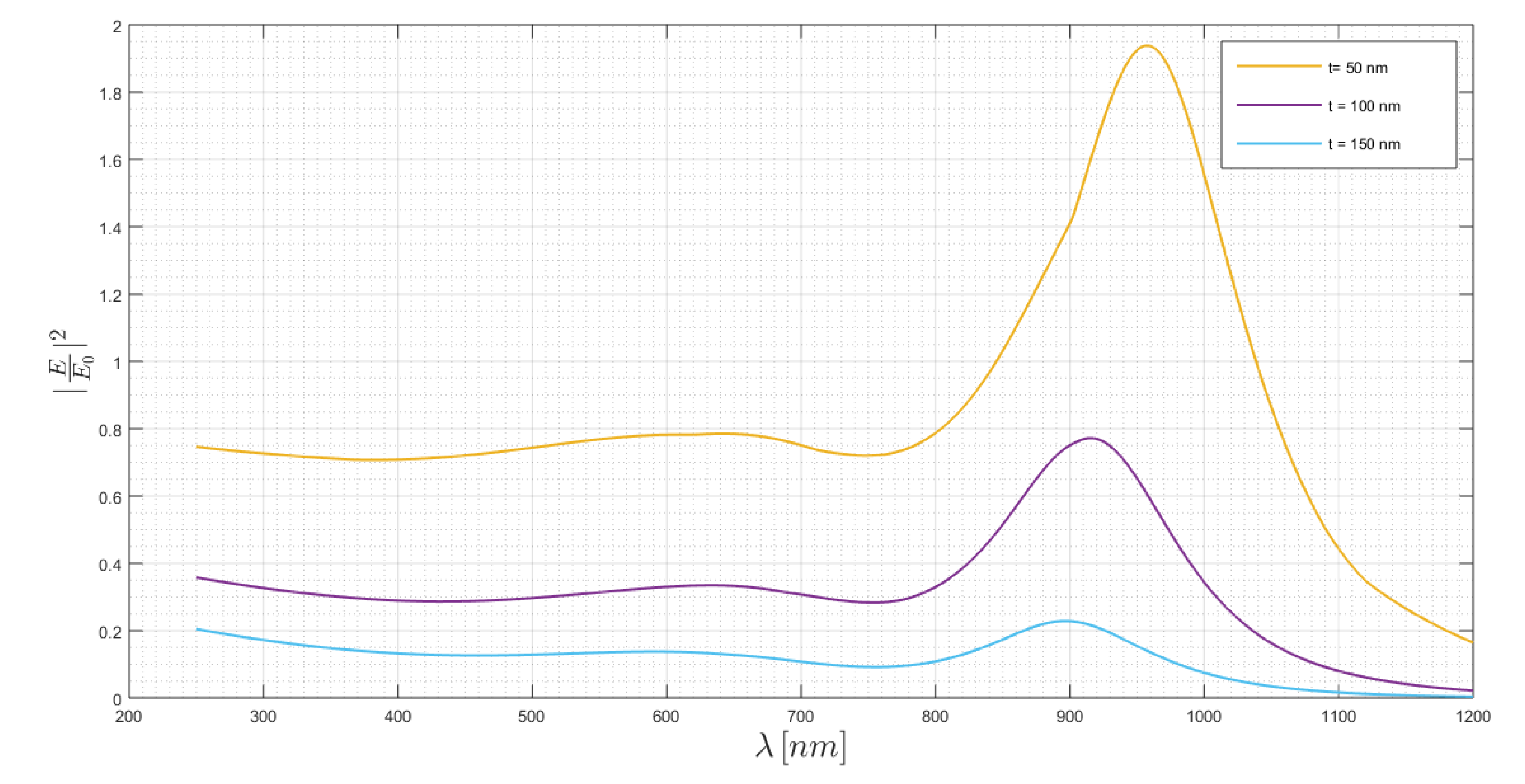
The nanoantenna thickness sweep is analyzed in this section. Here, it is very important to mention again that the nanoantenna was inside the dielectric medium. This one had a thickness of , so that when the nanoantenna thickness was varied, the air medium thickness was also varied. This is an important statement, because all the conclusions that could be made would continue to be based on the assumption that the distance between the port, where the electromagnetic wave was generated, and the nanoantenna rear, which was in contact with the “substrate”, remained constant.
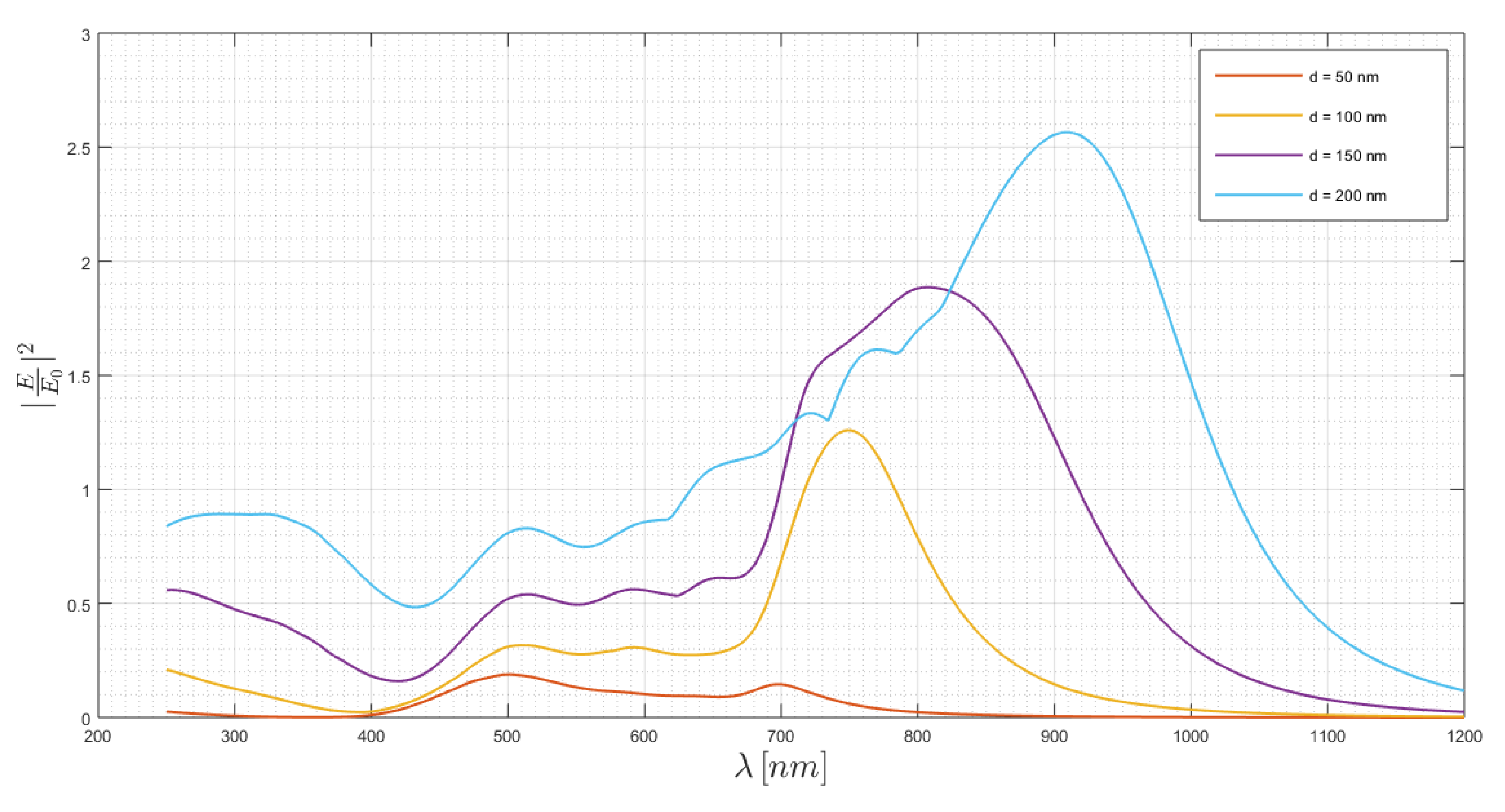
In Figure 11 is presented the behavior of silver. The less the nanoantenna thickness was, the higher the peak was, and also, the higher the peak wavelength was, then the red-shift occurred. The maximum achieved gain was 2.65 for , for an incident wavelength of .
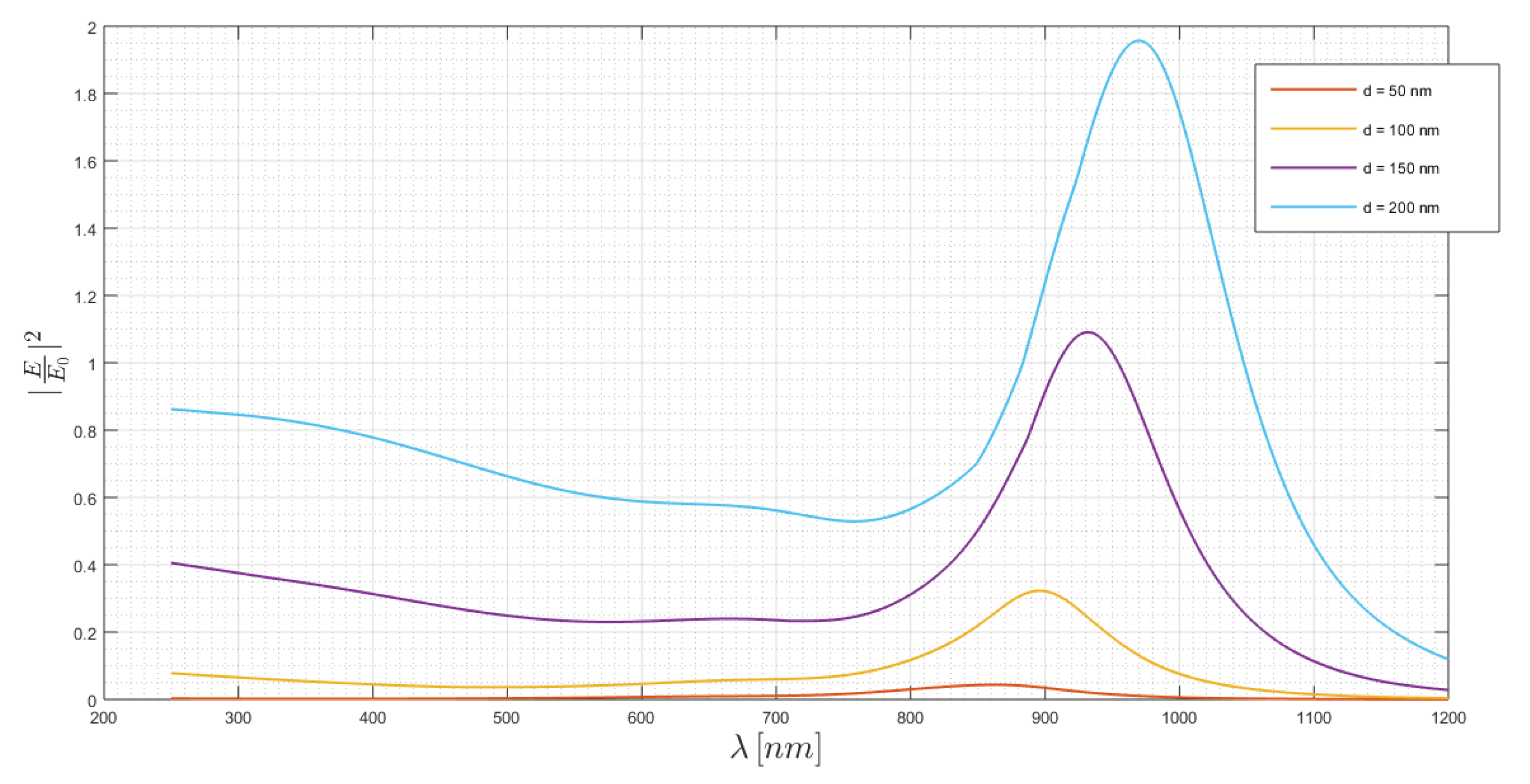
The same was registered for the gold and copper simulations, presented respectively in Figure 12 and Figure 13. Once again, it was suggested that both characteristic responses were similar, in spite of the sweep, registering a maximum gain of 2.18, for an incident wavelength of , for the gold nanoantenna in comparison with 1.94, for an incident wavelength of , reached with a copper one.
In the aluminum spectrum, presented on Figure 14, it was quite evident that increasing the thickness, a flatter gain region would be created. However, it was also obvious that the intensity maximum would be lower. Thus, it is an important tuning if a flatter region is needed, using other parameters to increase the gain and push this region to a higher intensity peak value. Furthermore, analyzing these curves, they seemed to reveal a blue-shift when the structure thickness became higher.
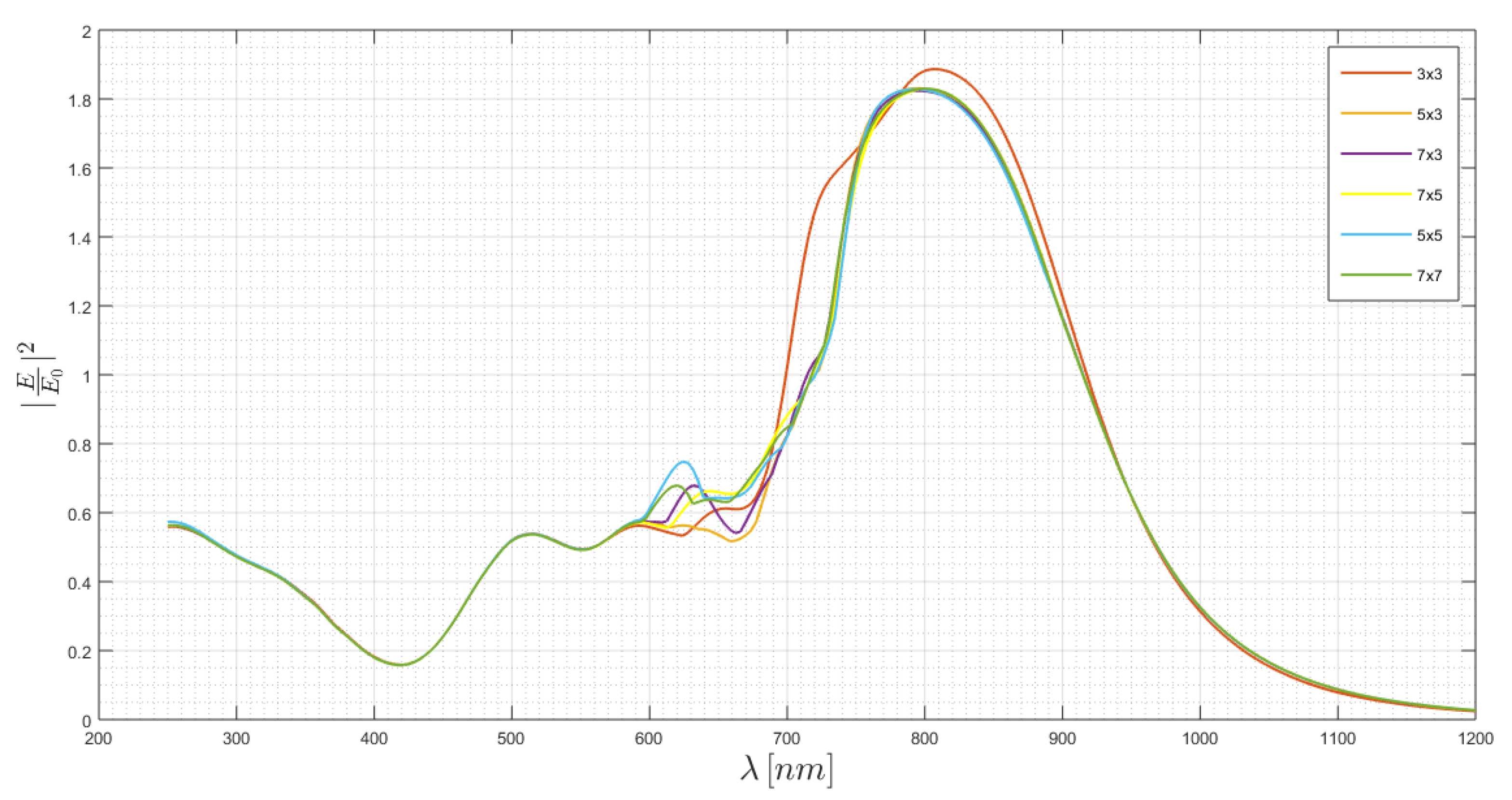
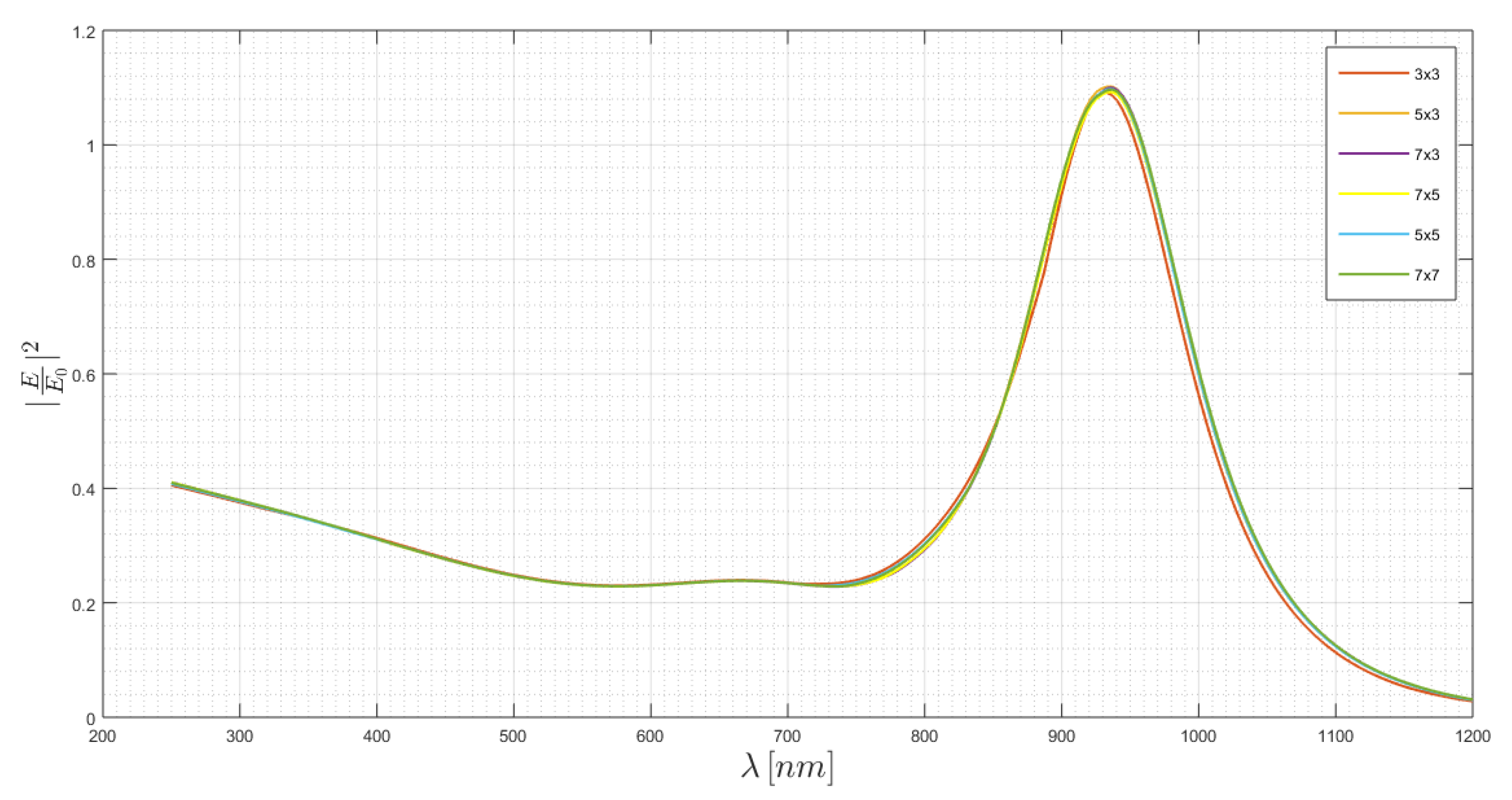
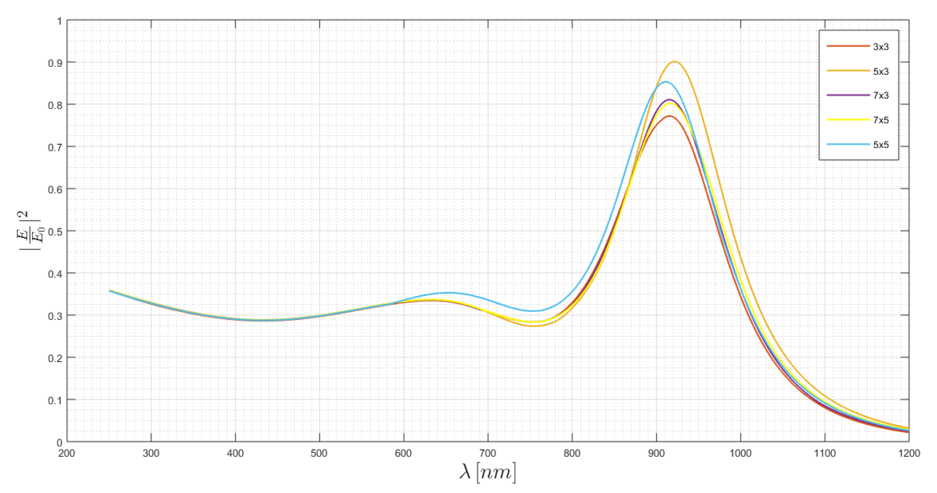
3.4. Number of Holes Sweep
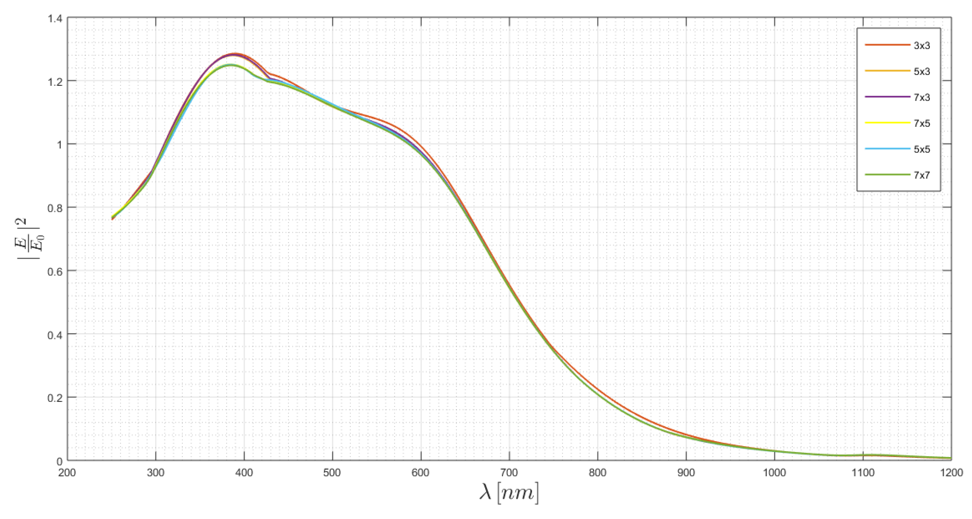
The last sweep considering air-metal-air interfaces was the variation of the number of holes that composed the nanoantenna. As the nanoantennas had a square lattice, what changed here was its number of lines and columns. For each metal, six different topologies were simulated, considering arrays of 3 × 3, 9 holes, 5 × 3, 15 holes, 7 × 3, 21 holes, 7 × 5, 35 holes, 5 × 5, 25 holes, and 7 × 7, 49 holes. Doing these simulations, several other geometrical aspects were imposed on the nanoantenna, related to its geometry, such as the different positions of the nanoantenna center, in a 3 × 3 array, the center was at the center of a hole, and the possibility to increase the number of adjacent holes, in a 3 × 3 array, only the center one had holes in its front, back, left, right, and all four diagonal directions.
In Figure 15 are presented the silver simulation results, where it is possible to observe that the overall spectrum did not vary greatly. The most visible variation happened on the minimum before the peak, the minimum due to Wood’s anomaly, where its value and shape changed. However, no rule seemed be able to express this variation, since the spectrum shape changed as well.
The gold nanostructure simulation set is presented in Figure 16. Considering these simulations, it was quite impressive that the optical response of the gold nanoantenna did not change when the number of holes was varied. Thus, it was possible to conclude, based on these values, that gold’s optical response was almost independent of the number of holes of a square nanoantenna.
Although gold and copper had similar optical responses, their behavior could be different when the parameters were swept. This parameter sweep allowed us to verify this. Whereas the gold response was almost independent of the number of holes, the copper resonant peak depended on it, as is possible to verify in Figure 17.
In Figure 18, it is possible to visualize the behavior of aluminum for this sweep. Based on this figure, it was possible to conclude that there were not very significant variations in the aluminum optical response.
4. Conclusions
This article aimed to study the parameter and material influence on the optical response of a nanoantenna. Considering the previous simulations, it was quite evident that each metal/plasma led to a different spectrum. Some spectra had a well defined resonant peak, for silver, gold, and copper; however, a flatter region could be reached using aluminum.
Furthermore, it was concluded that the optical response could be tuned by the structure parameters.
The main conclusion from the periodicity sweep was that the maximum intensity peak wavelength did not depend linearly on the periodicity. Considering the values of , , , and , there were materials where the peak value decreased as the periodicity increased (silver and gold), and other where no rule seemed to be valid (copper). The aluminum was in another category, because whereas silver, gold, and copper had a well defined peak and bandwidth, working almost as a band-pass filter in this frequency range, aluminum could work as a high-pass filter, for this specific range. Despite that its response analysis could be done focusing on the peak values, it was better to do it by spotlighting the amplification ripple, the response smoothness of the gain region, and the gain/attenuation difference between the gain region and the other wavelengths that must be attenuated. Depending on the application, these specifications could be given, and the structure could be tuned in order to accomplish it.
To summarize the conclusions about the hole diameter sweep, it was concluded that an adjustment done on the hole diameter allowed shifting the output spectrum within a certain wavelength range. Although the intensity peak could decrease greatly when varying the hole diameter, within the subwavelength condition, other parameter behaviors could be used to increase it. For instance, considering independent sweeps, other parameters could be used to increase the peak value, in order to be detectable.
Considering the study about the influence of the nanoantenna thickness, it could be stated that the thicker the nanoantenna was, the lower the maximum intensity peak would be, due to the increasing of the dispersion losses, which were proportional to the propagation length. Associated with this peak decay was a wavelength shift to the violet and ultra-violet region, a blue-shift. Moreover, the aluminum optical response was not, here, an exception; however, in addition to it, the aluminum gain region became flatter, when its thickness increased. This last conclusion had enormous importance, because both the thickness and hole diameter of a aluminum made nanoantenna could be adjusted together to create a flatter gain region, i.e., using the thickness to smooth it and the hole diameter to improve the gain. Further, increasing the hole diameter mainly led to a red-shift, or at least a predominant expansion of the gain region to the red side of the spectrum, whereas the nanoantenna thickness led to a blue-shift, so that the gain region band range could also be adjusted. Nonetheless, this conclusion was stated assuming that the structure parameters and their influence on the optical response were independent, such as tuning more than one parameter, the result being a spectrum that satisfied each independent tuning behavior.
The last conclusion was made based on the results from the number of holes study. These results showed that the gold and the aluminum spectra were almost independent of this sweep, whereas the copper resonant peak value and wavelength had a small variation, and the silver response differed in Wood’s minimum region. When the number of holes increased, the structure dimensions increased as well, so that, based on the last statement, if the manufacturer could not produce devices as small as the ones presented here, on the gold or aluminum structures, the device dimensions could be increased, by increasing the number of holes without having a trade-off in the output response. It is quite important to mention that a 5 × 3 and a 3 × 5 array were the same, because the incident electromagnetic field was orthogonal to the structure screen, and its magnitude was uniformly distributed for the other components. Thus, only one of these situations was presented in the figure. Furthermore, three numbers were used, 3, 5 and 7, in all of their combinations in order to show the optical responses when one and both dimensions, length and width, the x and y directions, were expanded.
These conclusions are very important to design this kind of nanostructure. The performance of some devices such as solar cells, LEDs, LASERs, or photodetectors can be improved using structures such as nanoantennas. Thus, it is quite important to develop studies as the one presented in this article, and even better if the models and equations are formulated and proven. These conclusions allowed us to analyze the influence of these parameters on the output response. In the future, using similar simulation environments, more studies focused on each parameter can be developed in order to determine analytical models for those specific cases, or theoretically analyze the electromagnetic field, in order to develop general equations and models. Having this, the design of these structures and their integration in devices can became easier and more efficient.
Author Contributions
R.A.M.L. was responsible for the investigation and for the manuscript writing. J.P.N.T. and A.B. are his supervisors. All authors read and agreed to the published version of the manuscript.
Funding
This research received no external funding.
Acknowledgments
This work was supported in part by FCT/MCTESthrough national funds and in part by EU funds under Project UIDB/EEA/50008/2020.
Conflicts of Interest
The authors declare no conflict of interest.
Appendix A
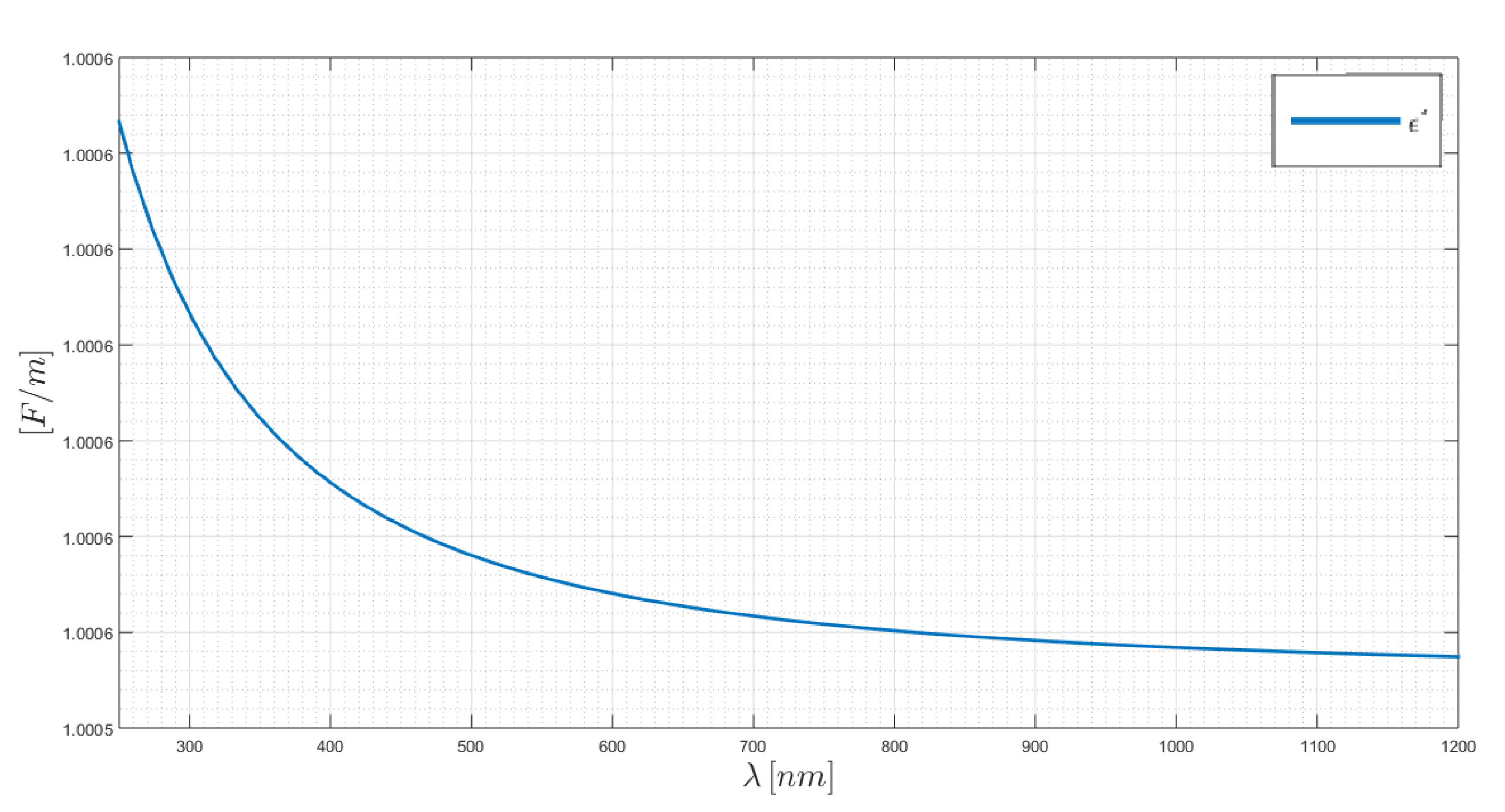
The complex dielectric function for each material is presented on this Appendix. As previously mentioned, the air dielectric function was fitted by Ciddor’s model. This model is available in COMSOL Multiphysics, and the function’s values are also available in [24]. On the other hand, silver, gold, copper, and aluminum are modeled by Rakic’s Drude–Lorentz fitting, also available in both sources. However, in [24], the model of the complex refractive index was presented, , where n is the refractive index and k the extinction factor, as analyzed in Expression (A1), where it is also possible to verify the relation between the complex refractive index and the complex dielectric function. Thus, the dielectric function can be divided into a real, , and an imaginary part, . Each of them are also mathematically related to n and k, as presented in Expressions (A2) and (A3).
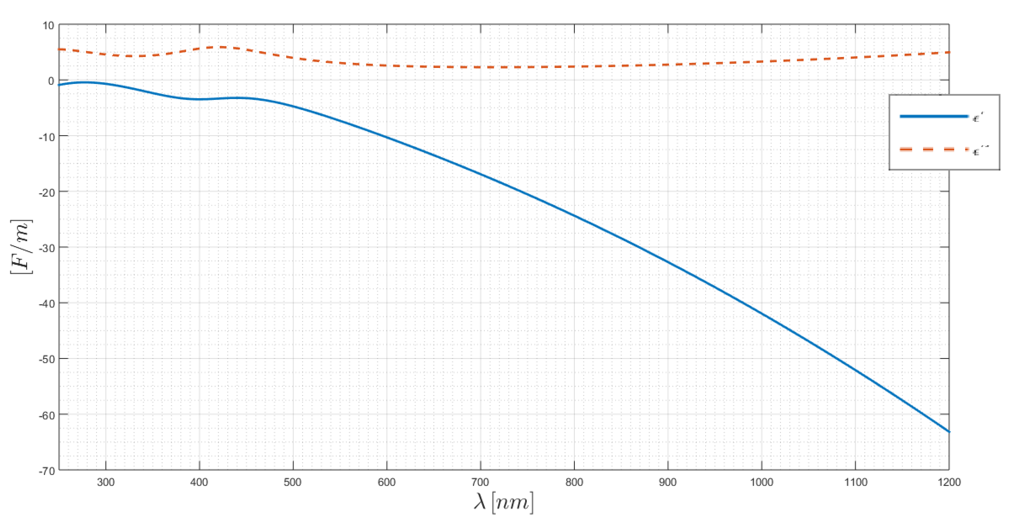
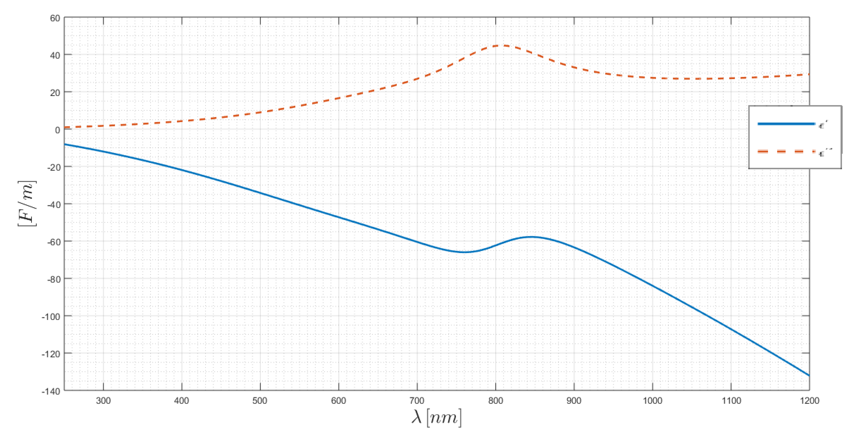
Considering the complex dielectric function model, the air fitting is illustrated in Figure A1, where it is possible to verify that this function has a null imaginary part. In Figure A2, Figure A3, Figure A4, Figure A5, the models for silver, gold copper, and aluminum are presented respectively. These figures allow verifying the analysis done for each material, regarding the expected peak position or output spectrum shape.
Figure A1.
Air complex dielectric function (solid blue line: real part).

Figure A2.
Silver complex dielectric function (solid blue line: real part; dashed red line: imaginary part).
Figure A2.
Silver complex dielectric function (solid blue line: real part; dashed red line: imaginary part).

Figure A3.
Gold complex dielectric function (solid blue line: real part; dashed red line: imaginary part).
Figure A3.
Gold complex dielectric function (solid blue line: real part; dashed red line: imaginary part).

Figure A4.
Copper complex dielectric function (solid blue line: real part; dashed red line: imaginary part).
Figure A4.
Copper complex dielectric function (solid blue line: real part; dashed red line: imaginary part).

Figure A5.
Aluminum complex dielectric function (solid blue line: real part; dashed red line: imaginary part).
Figure A5.
Aluminum complex dielectric function (solid blue line: real part; dashed red line: imaginary part).

References
- Lameirinhas, R.; Torres, J.P.; Baptista, A. Sensors Based on Nanoantennas: Fundamentals. Eur. J. Appl. Phys. 2020, 2. [Google Scholar] [CrossRef]
- Gomes, R.D.F.R.; Martins, M.J.; Baptista, A.; Torres, J.P.N. Study of a nano optical antenna for intersatellite communications. Opt. Quant. Electron. 2017, 49, 135. [Google Scholar] [CrossRef]
- Ebbesen, T.W.; Lezec, H.J.; Ghaemi, H.F.; Thio, T.; Wolff, P.A. Extraordinary optical transmission through sub-wavelenght hole arrays. Nature 1998, 391, 667. [Google Scholar] [CrossRef]
- Lalanne, P.; Hugonin, J.P. Interaction between optical nano-objects at metallo-dielectric interfaces. Nat. Phys. 2006, 2, 551. [Google Scholar] [CrossRef]
- Mohammadi, A.; Sandoghdar, V.; Agio, M. Gold, copper, silver and aluminum nanoantennas to enhance spontaneous emission. J. Comput. Theor. Nanosci. 2009, 6, 2024–2030. [Google Scholar] [CrossRef] [Green Version]
- Biagioni, P.; Huang, J.S.; Hecht, B. Nanoantennas for visible and infrared radiation. Rep. Prog. Phys. 2012, 75, 024402. [Google Scholar] [CrossRef] [Green Version]
- Wissert, M.D.; Schell, A.W.; Ilin, K.S.; Siegel, M.; Eisler, H.J. Nanoengineering and characterization of gold dipole nanoantennas with enhanced integrated scattering properties. Nanotechnology 2009, 20, 425203. [Google Scholar] [CrossRef]
- Gordon, R.; Sinton, D.; Kavanagh, K.L.; Brolo, A.G. A new generation of sensors based on extraordinary optical transmission. Acc. Chem. Res. 2008, 41, 1049–1057. [Google Scholar] [CrossRef]
- Marques, P.; Martins, M.; Baptista, A.; Torres, J.P.N. Communication Antenas for UAVs. JESTR 2018, 11, 90–102. [Google Scholar] [CrossRef]
- Carneiro, A.F.A.; Torres, J.P.N.; Baptista, A.; Martins, M. Smart Antenna for Application in UAVs. Information 2018, 9, 328. [Google Scholar] [CrossRef] [Green Version]
- Torres, J.P.N.; Baptista, A.; Machado, V.M. Analysis of semiconductor coupled waveguides with interband absorption. Opt. Quant. Electron. 2016, 48, 366. [Google Scholar] [CrossRef]
- Torres, J.P.N.; Baptista, A.; Machado, V.M. Analysis of dielectric optical ring slab waveguides with interband absorption. In Proceedings of the 2011 IEEE EUROCON—International Conference on Computer as a Tool, Lisbon, Portugal, 27–29 April 2011; pp. 1–3. [Google Scholar]
- Etezadi, D.; V, J.B.W.I.; Ruggeri, F.S.; Dietler, G.; Lashuel, H.A.; Altug, H. Nanoplasmonic mid-infrared biosensor for in vitro protein secondary structure detection. Light Sci. Appl. 2017, 6, e17029. [Google Scholar] [CrossRef]
- Sangwan, A.; Pandey, H.; Johari, P.; Jornet, J.M. Increasing the communication distance between nano-biosensing implants and wearable devices. In Proceedings of the 2018 IEEE 19th International Workshop on Signal Processing Advances in Wireless Communications (SPAWC), Kalamata, Greece, 25–28 June 2018; pp. 1–5. [Google Scholar]
- Ji, K.; O’Connell, J.G.; Carter, D.J.; Larson, D.N. High-throughput nanohole array based system to monitor multiple binding events in real time. Anal. Chem. 2008, 80, 2491–2498. [Google Scholar] [CrossRef] [PubMed]
- Prosposito, P.; Burratti, L.; Venditti, I. Silver Nanoparticles as Colorimetric Sensors for Water Pollutants. Chemosensors 2020, 8, 26. [Google Scholar] [CrossRef] [Green Version]
- Catchpole, K.R.; Mokkapati, S.; Beck, F.; Wang, E.C.; McKinley, A.; Basch, A.; Lee, J. Plasmonics and nanophotonics for photovoltaics. Mrs Bull. 2011, 36, 461–467. [Google Scholar] [CrossRef]
- Miyamichi, A.; Ono, A.; Kagawa, K.; Yasutomi, K.; Kawahito, S. Plasmonic Color Filter Array with High Color Purity for CMOS Image Sensors. Sensors 2019, 19, 1750. [Google Scholar] [CrossRef] [Green Version]
- Novotny, L.; Van Hulst, N. Antennas for light. Nat. Photonics 2011, 5, 83. [Google Scholar] [CrossRef]
- Sain, B.; Meier, C.; Zentgraf, T. Nonlinear optics in all-dielectric nanoantennas and metasurfaces: A review. Adv. Photonics 2019, 1, 024002. [Google Scholar] [CrossRef] [Green Version]
- Pavlov, D.; Syubaev, S.; Kuchmizhak, A.; Gurbatov, S.; Vitrik, O.; Modin, E.; Kudryashov, S.; Wang, X.; Juodkazis, S.; Lapine, M. Direct laser printing of tunable IR resonant nanoantenna arrays. Appl. Surf. Sci. 2019, 469, 514–520. [Google Scholar] [CrossRef]
- Rakhshani, M.R.; Mansouri-Birjandi, M.A. High sensitivity plasmonic refractive index sensing and its application for human blood group identification. Sens. Actuators B Chem. 2017, 249, 168–176. [Google Scholar] [CrossRef]
- Beermann, J.; Søndergaard, T.; Novikov, S.M.; Bozhevolnyi, S.I.; Devaux, E.; Ebbesen, T.W. Field enhancement and extraordinary optical transmission by tapered periodic slits in gold films. New J. Phys. 2011, 13, 063029. [Google Scholar] [CrossRef]
- Refractive Index Database—Refractive Index. Available online: https://refractiveindex.info/ (accessed on 17 April 2020).
Figure 1.
Simulation environment and structure illustration.

Figure 2.
Structure illustration focusing on the nanoantenna.

Figure 3.
Periodicity sweep on the silver nanostructure.

Figure 4.
Periodicity sweep on the gold nanostructure.

Figure 5.
Periodicity sweep on the copper nanostructure.

Figure 6.
Periodicity sweep on the aluminum nanostructure.

Figure 7.
Hole diameter sweep on the silver nanostructure.

Figure 8.
Hole diameter sweep on the gold nanostructure.

Figure 9.
Hole diameter sweep on the copper nanostructure.

Figure 10.
Hole diameter sweep on the aluminum nanostructure.

Figure 11.
Nanoantenna thickness sweep on the silver nanostructure.

Figure 12.
Nanoantenna thickness sweep on the gold nanostructure.

Figure 13.
Nanoantenna thickness sweep on the copper nanostructure.

Figure 14.
Nanoantenna thickness sweep on the aluminum nanostructure.

Figure 15.
Sweep of the number of holes that composed the silver nanostructure.

Figure 16.
Sweep of the number of holes that composed the gold nanostructure.

Figure 17.
Sweep of the number of holes that composed the copper nanostructure.

Figure 18.
Sweep of the number of holes that composed the aluminum nanostructure.

© 2020 by the authors. Licensee MDPI, Basel, Switzerland. This article is an open access article distributed under the terms and conditions of the Creative Commons Attribution (CC BY) license (http://creativecommons.org/licenses/by/4.0/).
Share and Cite
MDPI and ACS Style
Marques Lameirinhas, R.A.; N. Torres, J.P.; Baptista, A. The Influence of Structure Parameters on Nanoantennas’ Optical Response. Chemosensors 2020, 8, 42. https://0-doi-org.brum.beds.ac.uk/10.3390/chemosensors8020042
AMA Style
Marques Lameirinhas RA, N. Torres JP, Baptista A. The Influence of Structure Parameters on Nanoantennas’ Optical Response. Chemosensors. 2020; 8(2):42. https://0-doi-org.brum.beds.ac.uk/10.3390/chemosensors8020042
Chicago/Turabian StyleMarques Lameirinhas, Ricardo A., João Paulo N. Torres, and António Baptista. 2020. "The Influence of Structure Parameters on Nanoantennas’ Optical Response" Chemosensors 8, no. 2: 42. https://0-doi-org.brum.beds.ac.uk/10.3390/chemosensors8020042
Note that from the first issue of 2016, this journal uses article numbers instead of page numbers. See further details here.