Article

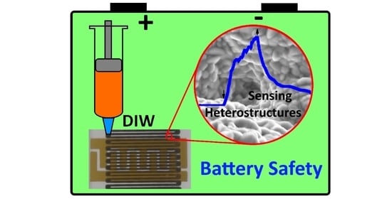
Additive Manufacturing as a Means of Gas Sensor Development for Battery Health Monitoring

1
Institute for Materials Science—Functional Nanomaterials, Faculty of Engineering, Kiel University, Kaiser Str. 2, 24143 Kiel, Germany
2
Center for Nanotechnology and Nanosensors, Technical University of Moldova, 168 Stefan cel Mare Av., MD-2004 Chisinau, Moldova
3
Department of Microelectronics and Biomedical Engineering, Faculty of Computers, Informatics and Microelectronics, Technical University of Moldova, 168 Stefan cel Mare Av., MD-2004 Chisinau, Moldova
4
Synthesis and Real Structure, Institute for Materials Science, Kiel University, Kaiser Str. 2, 24143 Kiel, Germany
5
National Nuclear Security Support Centre, Technical University of Moldova, 168 Stefan cel Mare Av., MD-2004 Chisinau, Moldova
6
Fraunhofer Institute for Silicon Technology (ISIT), Fraunhoferstrasse 1, 25524 Itzehoe, Germany
7
Multicomponent Materials, Faculty of Engineering, Christian-Albrechts Universität zu Kiel, Kaiser Str. 2, 24143 Kiel, Germany
*
Authors to whom correspondence should be addressed.
Submission received: 2 July 2021 / Revised: 24 August 2021 / Accepted: 30 August 2021 / Published: 6 September 2021

Abstract

:
Lithium-ion batteries (LIBs) still need continuous safety monitoring based on their intrinsic properties, as well as due to the increase in their sizes and device requirements. The main causes of fires and explosions in LIBs are heat leakage and the presence of highly inflammable components. Therefore, it is necessary to improve the safety of the batteries by preventing the generation of these gases and/or their early detection with sensors. The improvement of such safety sensors requires new approaches in their manufacturing. There is a growing role for research of nanostructured sensor’s durability in the field of ionizing radiation that also can induce structural changes in the LIB’s component materials, thus contributing to the elucidation of fundamental physicochemical processes; catalytic reactions or inhibitions of the chemical reactions on which the work of the sensors is based. A current method widely used in various fields, Direct Ink Writing (DIW), has been used to manufacture heterostructures of Al2O3/CuO and CuO:Fe2O3, followed by an additional ALD and thermal annealing step. The detection properties of these 3D-DIW printed heterostructures showed responses to 1,3-dioxolan (DOL), 1,2-dimethoxyethane (DME) vapors, as well as to typically used LIB electrolytes containing LiTFSI and LiNO3 salts in a mixture of DOL:DME, as well also to LiPF6 salts in a mixture of ethylene carbonate (EC) and dimethyl carbonate (DMC) at operating temperatures of 200 °C–350 °C with relatively high responses. The combination of the possibility to detect electrolyte vapors used in LIBs and size control by the 3D-DIW printing method makes these heterostructures extremely attractive in controlling the safety of batteries.

Graphical Abstract

1. Introduction

The development of solid-state sensors and sensor arrays with low costs and efficiency is a growing goal of the sensor community. Detecting potential hazards in mixtures or ionizing radiation is a challenging task that requires the determination of specific individual components positively and sensitively. For this purpose, the development of sensor arrays with a wide range of varying materials and performances/possibilities is necessary. Whereas many approaches are based on various synthesis steps, the automatic combination of many complex materials can easily be realized by e.g., additive manufacturing or three-dimensional (3D) printing [1]. A large variety of 3D printed sensors have been developed and manufactured recently in the field of biotechnology e.g., for detection of glucose [2], selected medicament [3], trace elements [4], neurotransmitters [5], nucleic acids [6] and/or proteins [7].
Sharafeldin et al. [1] pointed out that 3D printing is very promising even for the detection of cancer and other diseases, because these complex diagnostic devices could be simply connected to portable devices like smartphones with batteries [1]. Also the fabrication of strain sensors by 3D printing has been demonstrated by Liu et al. [8] using various printing methods, such as Digital Light Processing (DLP) and Direct Ink Writing (DIW) [8]. Han et al. [9] presented an overview of the challenges of current biomedical sensors [9]. The authors hint at some possible limitations, one of which is related to the biocompatibility of printed materials [9]. Another concern is related to their recyclability and reuse on the stability of the signal determination [9]. It is proposed that one of the solutions to improving this problem is the association of dynamic thresholds of Flexiforce Sensor [10]. Another idea is to increase the use of other materials to develop 3D printed sensors based on nanocomposites with optimized characteristics [9].
Not only biotechnology can profit from the rapid developments enabled by the 3D printing of sensors. Another rapidly growing field is the safety monitoring in Lithium-ion batteries (LIBs) [11,12], attributable to highly reactive components inside this type of battery. Regarding this type of battery, safety is a significant concern and it must be monitored carefully and reliably. Battery safety requires sensors for the detection of many different volatile compounds (e.g., C4H10O2, C3H6O3, 1,2-dimethoxyethane, dimethyl carbonate, C4H8O3) [13] that could be formed upon battery failure. Especially due to their use in portable electronics, such as computers or smartphones [14,15], or in electric or hybrid vehicles, safety monitoring is even more important and therefore, there is a need of suitable sensors that fit the requirements for the possible application [16]. Further, with the increase in LIB’s performance in terms of energy density and power density, the safety guarantee has not yet been fully addressed [17], thus the main causes of fires and battery explosions being the heat leakage and the presence of inflammable components [15,17,18]. One of the solutions proposed by Chen et al. [17] to secure the batteries against thermal and mechanical harm is the improvement of the outer casing [17]. Another solution is to mount the batteries in the parts of auto vehicles that are least affected during an accident [17] and to prevent the thermal runaway before sensors are indispensable.
For safer batteries related to their heating protection, Chen et al. [18] have developed a class of ultra-fast and thermo-responsive reversible polymer switching (TRPS) material, which consists of the use of graphene-coated, nano-spiked Ni particles on polymer composite films, thus demonstrating good battery characteristics at ambient temperatures and their rapid disconnection under abnormal regimes, such as overheating and short circuiting [18]. The generation of heat and its accumulation inside the batteries is often accompanied by the generation of flammable gas due to various parasitic reactions, therefore it is necessary to improve the safety of the batteries by preventing the generation of these gases. [15,17,19].
In particular, the generation of heat and its accumulation inside the batteries is often accompanied by the generation of inflammable gases, such as CO, H2, CH4, C2H4, C2H6, and C3H8 due to various parasitic reactions depending on temperature, electrolysis, electrolytes and the appearance of thermal leakage [13,20]. Therefore, it is necessary to improve the safety of the batteries by preventing the generation of these gases and/or by the implementation of suitable sensors for early hazard detection and rapid disconnection of the battery. Essl et al. [13] investigated, tested, and proposed the use of various gas sensing structures as early detectors of battery deterioration. Here, it is shown that sensing structures based on metal oxide semiconductors (MOX) are the most promising candidates due to their speed of response with high sensitivity, low cost, and their ability to easily connect to the battery management system (BMS) [13]. Following the studies, the authors mention that it is possible to detect battery failures with gas sensors, but through the many different failure mechanisms, ongoing study is still necessary [13].
The recent huge demand towards portable devices with precise sets of properties requires cost-effective materials and new approaches to fabricate devices out of these materials [19]. Based on that, 3D-DIW devices have attracted our consideration, due to their design potentiality as shown already e.g., for new strain sensing [21] or totally electronic components [22]. The progress in gas detecting and in 3D-DIW approaches will initiate larger capabilities to embody e.g., oxides directly onto multisensory or portable devices [23]. Previous reports claim that this 3D-approach will permit the assembly of multiple sensors through DIW for the precise sensing of specific vapors in various atmospheres, especially for battery safety. Thus, the development of a class of 3D-DIW nanomaterial consisting of semiconducting oxide particles, which can detect explosive vapor leakages and indicate on necessity of rapid disconnection battery under abnormal concentrations, such as C3H6O2, C4H10O2 vapors, electrolytes containing LiTFSI and LiNO3 salts in a mixture of DOL:DME, as well as to LiPF6 salts in a mixture of EC:DMC is highly demanded. Oxide-based nanostructures, especially a combination of p and n-type conductivity (CuO and Fe2O3), TiO2 and Al2O3/CuO and CuO:Fe2O3, are highly prominent investigated mixtures for gas sensors due to their response, stability, and good sensitivity [19,24,25,26].
This work reports on the use of the 3D-DIW printed nanocrystalline films tested as reliable, accurate, and selective sensors for the test of battery electrolytes vapor at relative concentrations. At this stage our input and aim is to promote battery safety through early leak detection, which we consider of high importance, especially for the electrification of the mobility sector and its large-format lithium ion batteries [13,17]. In the future, a tighter control of the reactions occurring inside the battery by monitoring the electrolyte composition via non-intrusive sensors may be a promising approach to improving the batteries’ lifetime and performance.
In the presented study, two different sensor concepts, both prepared via additive manufacturing, were demonstrated and investigated regarding their applicability for battery safety monitoring by studying their sensing properties in the presence of commonly used battery vapors, electrolytes, and solvents. This work will promote the 3D printing of such sensors for battery safety in premiere, e.g., to place a sensor outside a battery pack, or for it to be integrable into the pouch cell or inside the pouch cell, where it has direct access to the evolving gases in a smart battery device. This study is only to evaluate the additive manufacturing of nanomaterials as a means of gas sensor development to detect evolving gases, thus it is a first step in the sensor design.

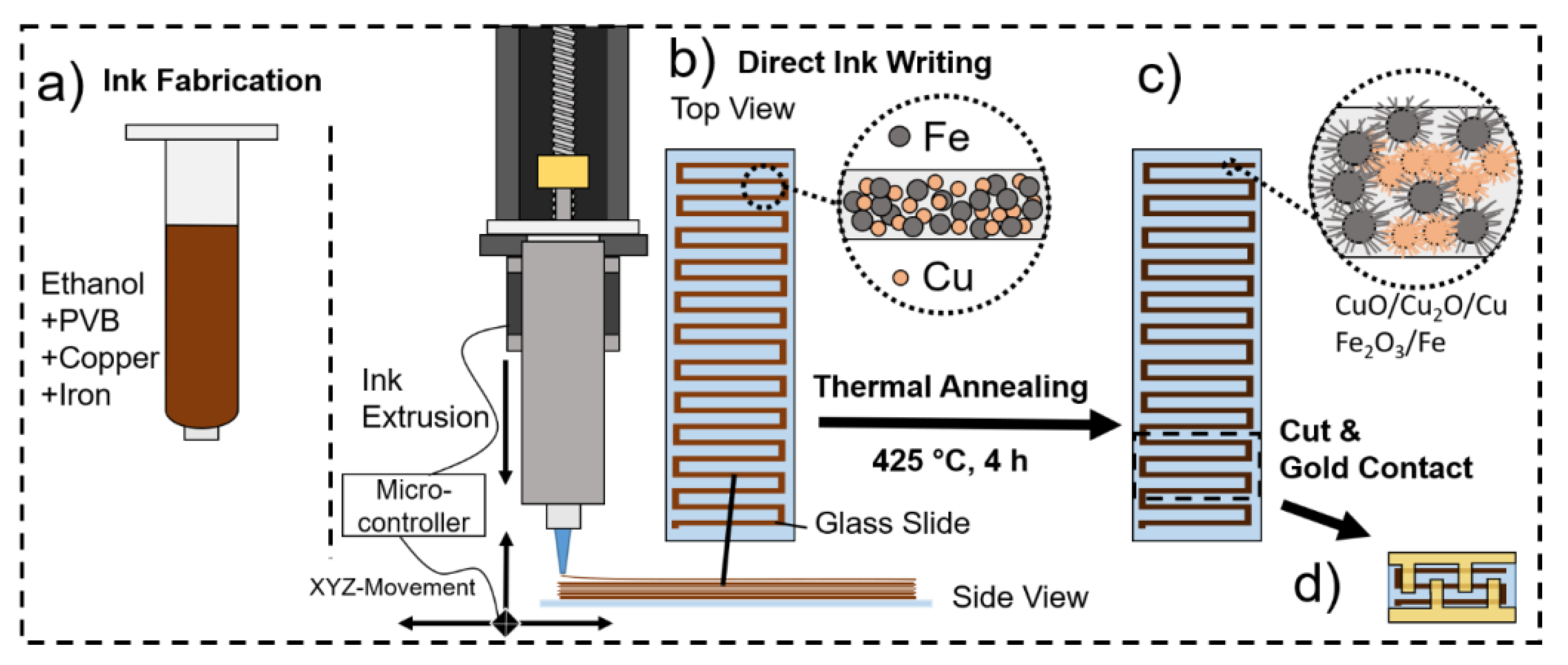
2. Materials and Methods
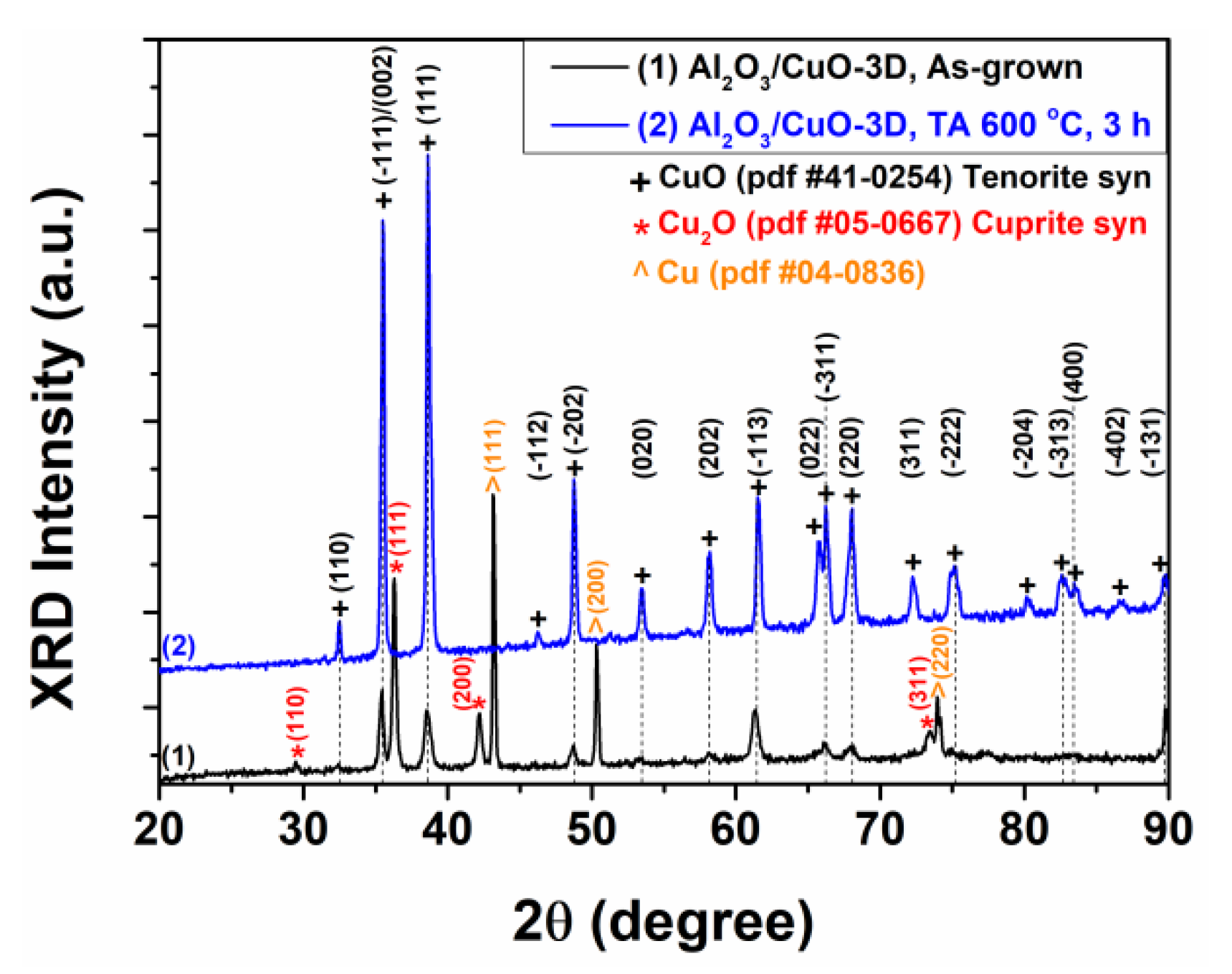
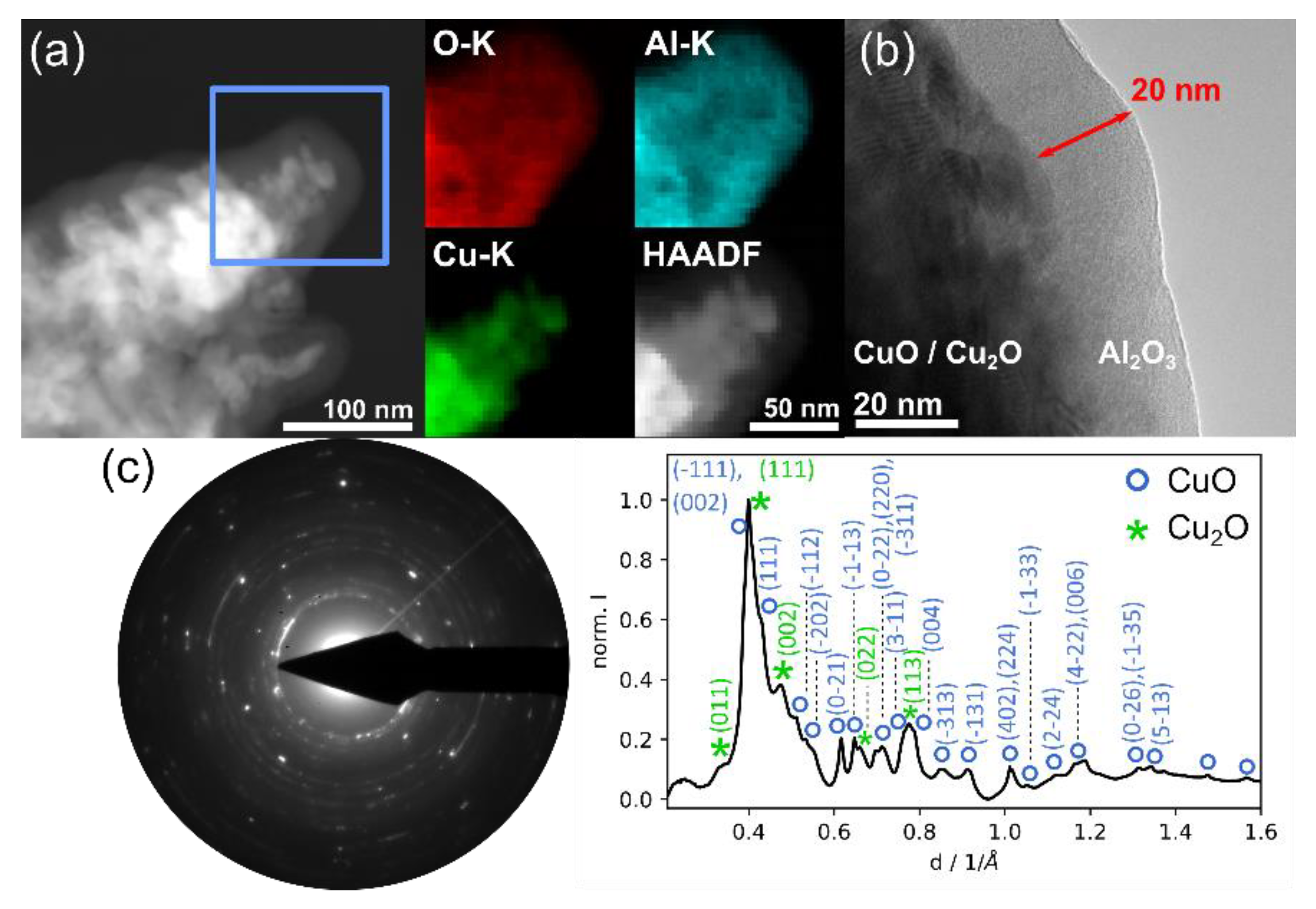
For the preparation of the sensor devices a single-step, 3D-DIW approach reported by Siebert and co-workers [23] in a recent article was used (see Figure 1). The Cu—based stripes/traces prepared by DIW were covered with nanowire arrays with a size of ~25 nm only after thermal annealing (TA) at 425 °C for 3 h in ambient temperature, thus forming CuO/Cu2O/Cu microparticles (MPs) bridge-lines. In the previous work, printed devices were mainly based on networked MPs stripes which possess a diameter of ~20 µm directly on the substrate, while in this work a subsequent thermal atomic layer deposition (ALD) of Al2O3 (20 nm) with a following TA at 600 °C for 3 h. Subsequently, the 3D-DIW Cu MPs-based layer/stripes developed a non-planar CuO/Cu2O/Cu structure totally covered with a 20 nm thin Al2O3 layer by ALD deposition. The samples of net bridging MPs were contacted externally with Au-contacts as reported [23].
The second set of sensors has been fabricated as stripes/traces by DIW using Cu-Fe, MP of Fe, and Cu particles (purity 99.9%) onto the substrate with a subsequent thermal annealing at 425 °C. The porous bridging nanostructures are made of heterojunctions which are connected via non-planar CuO/Cu2O/Cu nanowires/MPs and Fe2O3/Fe nanospikes/MPs as reported before [19]. Characterization of the nanomaterials was performed in detail as reported in our paper [19]. DIW, as a subdivision of additive manufacturing, alike to 3D-printing, as mentioned in several papers, facilitate the duration and productive creation of modern structures/systems with multiple levels of involvement for advancing technologies [19,27,28,29,30,31]. The fabricated 3D-printed mixed metal oxide nanomaterials arranged in stripes/traces will be shown with respect to battery vapor sensors featuring a flexible design concept, proving this approach to be the most attractive for the near future applications.
For the preparation of the Cu-based stripes/traces set of sensors, copper microparticles of ~20 µm in diameter were sonicated in H2O, then a powder of polyethylene oxide (Mv~2,000,000, Sigma-Aldrich, St. Louis, MO, USA) was added at 20 °C (see representation Figure 1a). Stripes were printed from MPs prepared as reported in Table 1 and discussed in detail previously [23]. The stripes/traces were DIW as a single layer through a custom apparatus (see representation Figure 1b). 3D stripes/traces were printed on the glass substrate in the current work as before (Figure 1b) [23]. Figure 1d shows the digital images of the representative samples after 3D printing and the samples being divided into individual sensors by interdigitating gold contacts.
The fabrication steps of the second set, or Cu-Fe-based sensor devices, is depicted in Figure 2. Initially, the fabrication of the rheological optimal ink was conducted (Figure 2a) based on Cu and Fe microparticles with a 96 vol% of C2H5OH, Polyvinyl butyral (PVB) (by Kuraray). The average diameters of the Cu and Fe microparticles were ~20 and ~50 µm, respectively [19]. The mixture ratios of the used ink were 3:1:1 (C2H5OH:PVB:metals) by weights and the metals’ MPs were mixed in a 1:1 ratio by weights. The ink was inserted in a 40 cm3 cartridge (Figure 2a) and left overnight before DIW, then loaded into a setup with a tapered nozzle (~0.59 mm) and stripped on the substrate (Figure 2b) [19]. For the next steps, the specimens were dehydrated for 22 h at 20 °C.
The DIW stripes/traces-based sensors were afterwards TA at 425 °C for 3 h and 600 °C for 3 h in an ambient atmosphere, both at a heating rate of 35 °C s−1 (Figure 2c). The temperatures for the TA used in the current work is changed compared to the previous works. The TA at 425 °C led to the formation of nanospikes and nanowires atop the MPs in the samples not covered with Al2O3, whereas the TA at 600 °C allowed for oxidation of the ALD treated MPs. Afterwards, gold contacts (~180 nm thick) were sputtered on top through a shadow mask onto each specimen (Figure 2d). The temperatures of the TA used in current and previous works are different.
Transmission electron microscope (TEM) investigation of the Al2O3/CuO-3D DIW heterostructures was performed with a FEI Tecnai F-30 G2 STwin (Thermo Fischer Scientific, Waltham, MA, USA) operated at 300 kV. Sample material was scraped off of the top of a finished CuO/Al2O3 sensor device after thermal annealing and placed on a Cu TEM (Plano GmbH, Wetzlar, Germany) grid in order to investigate the nanostructure of the deposited Al2O3 layer. To gain additional insight into the stoichiometry and chemical composition, the Al2O3/CuO-3D heterostructures were investigated by X-ray photoelectron spectroscopy (XPS, Omicron Full Lab., Omicron Nano-Technology GmbH, and non-chromatized Al-anode, 240 W, Taunusstein, Germany). Survey spectra were measured with a VSW hemispherical analyser at 100 eV pass energy, and high resolution spectra at 30 eV pass energy. After collecting the spectra, potential charging of the sample was corrected by setting the C-1s line of aliphatic carbon to the reference value of 284.5 eV [32]. For the evaluation the software CasaXPS (version 2.3.16) was used [33].
The gas-sensing properties measurements were performed continuously through a Keithley2400 source meter using LabView software (from National Instruments), as described in previous works [34,35]. The gas and vapor responses were calculated according to Equation (1), where Rgas and Rair represent the electrical resistances of the samples exposed to gas/vapors and under normal environmental conditions, respectively [36,37]:
S p = R g a s R a i r R a i r 100 % .
For testing the sensing properties of commonly used battery electrolytes, different samples were prepared. The electrolyte labeled as E1 is prepared by dissolving 0.7 M of lithium bis (trifluoromethanesulfonyl)imide (LiTFSI, Sigma-Aldrich, St. Louis, MO, USA) and 0.25 M of lithium nitrate (LiNO3, Sigma-Aldrich) in 1,3-dioxolane and 1,2-dimethoxyethane (v/v = 1/2) solvents (both Sigma-Aldrich). The electrolyte labeled as LP30 was used as received (Sigma-Aldrich) and is composed of 1M of LiPF6 in EC:DMC (v/v = 1/1). Further, the pure solvents 1,3-dioxolane and 1,2-dimethoxyethane labeled as C3H6O2 and C4H10O2, respectively, were also investigated.

3. Results

3.1. 3D-DIW Chemosensors Based on Semiconducting Oxide Nanostructures on CuO/Cu2O/Cu Heterojunction Net with Al2O3 Coating for Battery Safety Applications

Studied samples were printed from suspensions with 1.5:1.0 Cu:H2O weight ratios as reported in Table 1 and in our previous paper [23]. Afterwards, samples were thermally annealed and integrated into a sensor structure for further studies.
SEM images (Zeiss Gemini Ultra55 Plus, Oberkochen, Germany) of the prepared Al2O3/CuO-3D heterostructures after a second thermal annealing (TA) at 600 °C for 3 h in ambient conditions are presented in Figure 3. At low magnification (Figure 3a), Cu microparticles deposited on the glass substrate can be observed. MPs that were ALD coated with a thin layer of Al2O3 and subsequently TA at 600 °C for 3 h show a relatively homogenous surface structure (see Figure 3a). Figure 3b,c show micro agglomerations formed of Al2O3/CuO-3D heterostructures with diameters in the range of 12–20 µm from oxidized MPs, which entirely covered the device substrate and appear as a non-planar structure on the DIW stripes/traces. Figure 3d shows the formation of structured and interconnected crystallites of Al2O3/CuO on the surface of the oxidized Cu MPs with diameters in the range of 150–600 nm. A similar behavior was also observed for SCS deposited copper oxide layers in our previous papers after TA at 650 °C [37,38].
To determine the lattice parameters for the monoclinic structure and the unit cell volume for CuO, Equation (2) was used [39]:
1 d 2 = 1 s i n 2 β ( h 2 a 2 + k 2 s i n 2 β b 2 + l 2 c 2 2 h l   c o s   β a c ) .
The structural parameters of the Al2O3/CuO-3D heterostructures indicate no significant changes in values in comparison to previous studies [38].
The XRD patterns of the Al2O3/CuO-3D-DIW heterostructures are presented in Figure 4 (pattern 1 for as-grown and pattern 2 for TA at 600 °C for 3 h). For the as-grown structure (pattern 1), the presence of CuO, Cu2O and metallic Cu phases is evidenced. After thermal annealing (pattern 2), all significant reflections are attributed to CuO (pdf #41-0254, Tenorite syn) with the highest intensity for the (−111/002) and (111) reflections at angles of 35.53° and 38.64°, respectively. Reflections related to the crystalline phases of Al2O3 were not detected, strongly indicating an amorphous Al2O3 layer. For copper and iron oxide heterostructures fabricated by the 3D printing process, the XRD pattern is presented in Figure S1 (Supplementary Material). From XRD data the presence of CuO and Fe3O4 phases, as well as of Cu2O, Fe2O3, metallic Cu, and metallic Fe is evidenced.
In Figure 5a a high angle annular dark field (HAADF) scanning TEM (STEM) (Thermo Fischer Scientific, Waltham, MA, USA) micrograph of the edge of a CuO/Cu2O microstructure is shown. From HAADF-STEM Z-contrast a core region consisting of heavier elements and a shell/layer region containing lighter elements (or lower mass thickness) becomes visible. By using STEM-EDX mapping of the elemental distribution it is shown that the layer contains aluminum oxide, while the inner region is made up of copper oxide. The homogenous distribution of the O-K signal shows that both areas are oxidized. From high-resolution TEM (HRTEM) micrographs of the edge region shown in Figure 5a, it is revealed that the Al2O3 layer is amorphous and has a thickness of ca. 20 nm, cf., example in Figure 5b.
To investigate the crystal structure of the sample selected area electron diffraction (SAED), patterns are taken from a larger sample area including the area shown in Figure 5a. The SAED pattern in Figure 5c is characteristic for a polycrystalline sample, which is in agreement with both Figure 5a,b where the inner CuO region appears non-homogenous in HAADF-STEM Z-contrast, as well as in the HRTEM phase contrast. By looking at the rotational average of the SAED pattern in Figure 5c, reflections assigned to monoclinic CuO and Cu2O are identified. This is in agreement with previous findings for CuO nanostructures prepared in a similar way [40]. The presence of Cu2O in contrast to the XRD analysis can be attributed to an assumed smaller crystallite size of Cu2O after annealing, which might be below the detection threshold of coherently scattering domains by XRD. From the homogenous distribution of the Al2O3 layer seen in Figure 5a and the intact layer observed in Figure 5b, Al2O3 particle formation, as well as diffusion into the CuO, can be ruled out. This is supported by the fact that no crystallization of the Al2O3 has occurred for the given annealing temperatures (Figure 5c). In Figure S2 (Supplementary Material) a TEM investigation of copper and iron oxide nanostructures without deposition of an alumina layer are shown. The formation of crystalline CuO and Fe3O4 nanowires is demonstrated. Iron oxide nanowires appear to be formed with slightly smaller diameters than the CuO nanowires.
In Figure 6 the Raman spectrum of the Al2O3/CuO-3D heterostructures at room temperature, enfolded by 75 and 1000 cm−1, is shown. From Figure 6, the mode peaks depicted at 273 cm−1, 327 cm−1, and 610 cm−1 were designated to the CuO [38]. As in the case of the XRD and SAED measurements, no crystalline Al2O3 phase was detected, which again confirms its amorphous state as demonstrated by TEM on AlOx. For the CuO structures, the zone-center optical-phonon modes are presented in Equation (3) [41]:
Г = A g + 2 B g + 4 A u + 5 B u .
Thus, there are nine optical modes, where 3 modes ( A g + 2 B g ) are Raman active [41,42] and 3 A u + 3 B u are infrared active [38,43].
Compositional images taken by energy dispersive X-ray spectrometry (EDX) (Zeiss Gemini Ultra55 Plus, Oberkochen, Germany) elemental mappings of the Al2O3/CuO-3D heterostructures after TA at 600 °C for 3 h are presented in Figure 7. Based on the EDX studies, a Cu content of 43.08 at%, an O content of 52.72 at%, and an Al content of 4.21 at% in Al2O3/CuO-3D samples was detected, see Figure S3 (Supplementary Material). In addition, Figure S3 (Supplementary Material) shows the EDX spectrum of the Al2O3/CuO-3D heterostructures, where peaks of Cu, O, and Al can be distinguished. The estimated [Cu]:[O]:[Al] ratio by EDX analysis (see Figure S3, Supplementary Material) indicates the formation of Al2O3/CuO DIW stripes/traces. Uniform distribution of Cu, O and Al elements is observed in the investigated areas. Such results were also confirmed by EDX line scans taken along three micro particles of CuO covered with a thin layer of Al2O3, which are shown in Figure S4 (Supplementary Material), respectively.
The XPS investigation of the Al2O3/CuO-3D heterostructures with thermal annealing (TA) at 600 °C for 3 h indicates the presence of O, C and Al, which can be detected in the XPS overall spectrum, as depicted in Figure 8a. The signal corresponding to C stems from surface contaminations by atmospheric carbon. The signal corresponding to Al is attributed to the Al2O3/CuO-3D heterostructures. The O-1s is mainly related to Al2O3, although small contributions from atmospheric contaminations may also be contributing. [33]. A closer look at the high-resolution spectrum of the Al-2p signal, presented in Figure 8b, reveals that the main peak of the Al-2p line is located around 73.5 eV. The Al-2p3/2 and Al-2p1/2 lines are not resolved. The peak position around 73.5 eV agrees well with Al3+ in Al2O3, which is always present between 73.7 eV and 74.8 eV [32,44]. No Cu 2p lines are visible in the region between 920 and 950 eV. This indicates that the Cu concentration in the topmost 5–10 nm is below the XPS detection limit of approximately 0.1%. It appears that the CuO is completely covered with Al2O3.
The gas-sensing performances of the synthesized structures were measured in the presence of two, typically used battery electrolytes (E1 and LP30) and two individual solvents (C3H6O2 and C4H10O2) to simulate their probable response during leakage of an LIB. The results can be seen in Figure 9a. Here, the gas response was determined from Equation (1) and the electrical conductivity indicated p-type conductivity behavior of the investigated DIW stripes/traces [36,45].
Figure 9a shows the gas response to different commonly used battery electrolytes and their solvents with a concentration of 100 ppm at various operating temperatures of the synthesized, 3D printed Al2O3/CuO heterostructures. From Figure 9a it can be found that at low operating temperatures of 200 °C and 250 °C, the Al2O3/CuO-3D samples are more selective to the C3H6O2 vapor with responses of approximately 11% and 13%, respectively. At operating temperatures higher than 300 °C and 350 °C, the samples are more selective to the C4H10O2 vapor with the response’s values of approximately 16% and 16%, respectively. Based on the investigations of Essl et al. [13] the temperatures at which the leaked gases and vapors begin to appear in a real battery system is from ~120 to 140 °C and increasing temperatures can reach the thermal runway (TR), which means that our heterostructures can be used for Lithium-ion battery technology applications. Figure 9b shows the I/V-characteristics at different operating temperatures of 3D printed Al2O3/CuO heterostructures. From Figure 9b it can be seen that the samples have a non-linear I-V characteristic.
Figure 10 shows the real dynamic responses of the 3D-DIW Al2O3/CuO heterostructures exposed to 100 ppm of C3H6O2 (Figure 10a) and C4H10O2 (Figure 10b) in air. From Figure 10a the response to C3H6O2 is approximately 11% at an operating temperature of 200 °C with response and recovery/decay times of τr = 19.2 s and τd > 25 s, respectively. From Figure 10b the response to C3H6O2 is approximately 16% at operating temperatures of 300 °C and 350 °C with response and recovery/decay times of τr = 14.1 s and τd > 15 s, and τr = 16 s and τd > 15 s, respectively.

3.2. Characteristics of Semiconducting Oxide Nanostructures by Direct Ink Writing of Metal Microparticles and Their Potential Application as Battery Safety Sensors

Copper and Iron microparticles are used in that study because these metals form oxide nanowires and nanoflakes of CuO and Fe2O3, respectively. CuO is found to be a p-type semiconductor and Fe2O3 is an n-type semiconductor. These two may form p-n-junctions with space charge regions that are very sensitive towards changes in the electronic configuration of the individual constituents. On a more general note, this approach demonstrates the faculties that are enabled by utilizing 3D printing or additive manufacturing as a means of gas sensor development for battery health monitoring. By integrating more than one particle type into one sensor the capabilities of quick and simple sensor integration are demonstrated for 3D printing or additive manufacturing.
Figure 11a shows the response of the 3D printed copper and iron oxide heterostructures to the previously used samples with a concentration of 100 ppm at different operating temperatures. From Figure 11a it can be seen that at a low operating temperature of 250 °C, the samples are more selective to the C3H6O2 vapor with responses of approximately 28%. At operating temperatures higher than 350 °C, the samples are more selective to the vapor formed by the decomposition of the E1 electrolyte with the response value of approximately 46%. Figure 11b shows current-voltage characteristics for 3D printed copper and iron oxide heterostructures at different OPT. Experiments were conducted on several devices which all demonstrate the same behavior and exhibit ohmic contact behavior, thus the detection process can be assumed to be unaffected.
Figure 12 shows the real dynamic response curves of the 3D-DIW copper and iron oxide heterostructures exposed to 100 ppm of C3H6O2 (Figure 12a) and E1 (Figure 12b) in air. From Figure 12a the response to the C3H6O2 is approximately 28% at an operating temperature of 250 °C with response and recovery/decay times of τr = 9.4 s and τd = 21.8 s, respectively. From Figure 12b the response to the E1 vapor is approximately 46% at an operating temperature of 350 °C with response and recovery/decay times of τr = 6.7 s and τd > 15 s, respectively.
The proposed detection mechanism of the Al2O3/CuO-3D and 3D printed copper and iron oxide heterostructures is based on physico-chemical reactions on the surface of the heterostructures, which take place at different operating temperatures, is still under debate. As mentioned by Essl et al. [13] in the range of temperatures of ~120–140 °C, the first failures of the battery cells take place, such as electrolyte vaporization, heat generation, dangerous emissions of vent gases, the composition of toxic vent gases, and the emission of particles. At even higher temperatures thermal runway (TR) takes place [13].
Thus, based on the sensor data of the Al2O3/CuO-3D heterostructures, the operating temperatures at which the highest response for the C4H10O2 vapors was obtained is 300 °C and 350 °C, and knowing from the literature that at temperatures higher than 150 °C on the copper oxide surface adsorbed oxygen species, thus generating voids according to Equation (4) [23,46]:
1 2 O 2 ( gas ) 150 O ( ads ) + h + .
According to SEM images (Figure 3d) it is observed that on the surface of Cu MPs interconnected structures of Al2O3/CuO-3D are formed. This formation increases the surface/volume ratio, which is beneficial for sensory applications. Thus, when the C4H10O2 vapor is introduced into the test chamber, it will interact with the oxygen species adsorbed on the surface, generating carbon dioxide and water molecules and as a result, will increase the electrical resistance of the heterostructure. In the case of the 3D printed copper and iron oxide heterostructure, the detection mechanism for acetone vapor is described in the previous work [19], and is similar in this case only as to the E1 vapors.

4. New Perspectives

Nanostructured materials and applications are used in a large variety of domains, including radiative environments. The application of nanotechnologies for the nuclear/ionizing radiation field has been demonstrated from the 1970s to the 1980s [47]; however, the prefix “nano-” has not been used in materials with these configurations [48]. Among the applications, we note the method of increasing the efficiency of nuclear fuel combustion by nanoadditives, or hardening the steel by adding 0.5% by mass of Yttrium Oxide NPs, or 0.37% by mass of F2O3 nanoparticles. In some materials of the nuclear industry, it is observed that the irradiation of the formation of new ordered, nanostructured phases resulted contrary to the expectations of improving the mechanical properties. The usefulness of nanomaterials has also been demonstrated in the manufacturing of radiation protection clothing with a four times higher radiation absorption efficiency [49].
Nanotechnologies and semiconductor physics are some of the most promising areas of research and applications. Nanocrystals from semiconductors display size-dependent optical and electronic characteristics. Such nanomaterials with crystalline structures bridge the gap among small molecules and large crystals, demonstrating discrete electronic transitions reminiscent of isolated atoms and molecules, in addition to enabling the use of the useful unknown earlier performances of crystalline materials. Moving on to nanodimensions, we create absolutely new conditions for transport effects with respective consequences.
When switching to nanodimensions in semiconductor heterostructures, the increase of energy barriers can be useful in limiting the movement of load carriers, thus, in nanodimensional conditions, this opens new perspectives for highlighting the importance of quantum effects and their applicability. The transition to nanodimensions essentially changes the properties of material—for example, the forbidden band in quantum dots depends on the size of the quantum dots. For these reasons, obtaining different consecutive nanoconfigurations of one and the same material allows us to speak of a completely new material, although it has the same chemical formula and manifests itself with radically different (physical, chemical, optical…) properties from the three-dimensional macroscopic material. We conclude again that nanostructures open new horizons in materials science and nanoelectronics.
Our interest in various research on semiconductor nanostructures in ionizing radiation fields is driven by our expectations regarding: technological applications, which can induce structural changes of irradiated environments, thus contributing to the elucidation of fundamental physico-chemical processes; catalytic reactions or inhibitions of chemical reactions and other technological processes; reliability of nanostructured semiconductor materials in ionizing radiation fields; devices for securing the control of radioactive and nuclear materials (custom control); devices for radiation protection control; and making new protective materials.
We know the wide use of robots in ionizing radiation environments (nuclear power plants, nuclear waste facilities, deep space exploration, etc.). Thus, the impact of radiation on critical components of robots, such as LIBs (its electrolyte materials), is an urgent issue. For these reasons, we are again interested in the durability of sensors that monitor the work of LIBs.
Nanostructured media allow us to measure ionizing radiation with greater accuracy than do single crystals, because we have greater experimental control over the parameters governing the detector: the size and shape of NPs, compared to a single crystal, in which the presence of defects and impurities will decrease sensor performance. Therefore, nanostructured materials can be designed as materials for the next generation of ionizing radiation detection. The adaptation of this depends on overcoming the expected difficulties associated with the use of a composite material, consisting of countless interfaces at which information can be lost.
If we talk about perspectives in medicine, the radiation protection effects of NPs, such as ZnO, carbon, characterized by strong antioxidant properties, have an important role in protecting cells against DNA damage induced by ionizing radiation. The excellent biocompatibility of some metal oxides, ZnO NPs are among the most popular oxide, NPs in biological applications due to their excellent biocompatibility, economic, and low toxicity [50].
In analyzing the role of nanostructured semiconductor oxides, there is no doubt in the presence of ZnO as a sensor for a wide range of gases or toxins. ZnO (intrinsically or doped with impurities, is a semiconductor with a high band gap (Eg = 3.37 eV), characterized by a lower impact of nuclear radiation compared to Si, GaAs, and GaN. The scintillator synthesis on glass substrates indicates that it can be a promising material system for the detection of alpha radiation. The evaluation was performed at different sources of alpha radiation demonstrating a high sensitivity and reproduction of the results from 5% (high alpha radiation activities) to 20% (very low alpha radiation activities) [51].
Another eloquent example refers to X-ray sensitive ZnO nanofilms for medical radiodiagnosis. The experimental data indicated that the zinc oxide device possesses some increase in its sensitivity to the ionizing radiation as the X-ray effective energy decreases, unlike other types of semiconductor electronic devices frequently used as an X-ray detector [52]. It should be noted that ZnO sensors also have a dual application, such as the application of UV sensors as a scintillator for X-ray detection [53]. In combination with the metal contacts in Au and Ag, the ZnO sensors improve the substance of their luminescence parameters [54].
A new use of NPs from oxides of different elements, such as Al2O3, SiO2, Sc2O3, TiO2, V2O5, Cr2O3, MnO2, Fe3O4, CoO, NiO, CuO, ZnO, ZrO2, MoO3, Nd2O3, Sm2O3, Eu2O3, Gd2O3, Er2O3 and HfO2 are studied as radiosensitizing perspectives. The results inspire optimism for the use in radiotherapy and radiodiagnosis [55]. The role of nanostructures in the detection of various gases, or ionizing radiation, is expected to be developed especially in p-n structures, CMOS, various strip detectors, AC coupled strip detectors, double strip detectors, pixel detectors, hybrid pixel detectors, various drift detectors, different SSD, and other bi/three nanodimensional structures.

5. Conclusions

This work reports the response of the 3D printed Al2O3/CuO, as well as copper and iron oxide heterostructures, to various vapors of battery electrolytes and typically used solvents with a concentration of 100 ppm at different operating temperatures. For Al2O3/CuO-3D heterostructures, the detection of the C3H6O2 vapors with a response of approximately 11% at an operating temperature of 200 °C was realized, with response and recovery/decay times of τr = 19.2 s and τd > 25 s, respectively. However, at operating temperatures higher than 300 °C and 350 °C, the higher response is to C4H10O2 with a gas response value of approximately 16% showing response and recovery/decay times of τr = 14.1 s and τd > 15 s, and τr = 16 s and τd > 15 s, respectively. For the 3D printed copper and iron oxide heterostructures, it was found that at a low operating temperature of 250 °C, the samples showed the highest response to the C3H6O2 vapor with responses of approximately 28%. However, at operating temperatures higher than 350 °C, the samples are more selective to the vapors formed by the degradation of the E1 electrolyte with a response value of approximately 46%. As a continuation of our research, different metal and semiconductor oxides are characterized by various techniques, demonstrating unique electrical, structural, and optical properties, which allow their use in various detection devices. A promising area of nanostructured sensors is gas or vapor detection. TEM, as well as SEM investigations, confirmed the formation of a homogenous, 20 nm thick Al2O3 layer atop the CuO microstructures via ALD. The formation of this heterojunction alters the gas response compared to the CuO/Fe2O3 system and thus allows to tailor the sensors to its intended application. The processes involved in detecting gases with metal/semiconductor oxides are complex and require a fundamental understanding of the physico-chemical interactions between gas molecules and the surface. There is no doubt that nanostructured oxides will play a significant role in the upward development of gas sensors based on them with improved detection performances. Their electrochemical, optical, and radiative detection properties have a significant impact on monitoring the environment, health, and sustainability of the operation of various devices based on (electro-) chemical reactions. The surfaces of metal and semiconductor oxides have been recommended as the performance basis for functionalization and biofunctionalization, demonstrating high stability, sensitivity, and selectivity to a variety of molecules needed to be identified/controlled. The technological realization of the nanodimensions of the sensors based on oxides ensures a large contact surface that determines increased sensitivity and resolution. Electronic, optical properties, and selectivity of sensitivity to harmful components can be managed by technological doping, the formation of nanocomposites, and heat or radiative treatments. Regarding place to mounted or 3D printed such sensors for battery safety, is not only possible or imaginable to place a sensor outside a battery pack, but it might also be integrable into the pouch cell or inside the pouch cell, where it has direct access to the evolving gases. However, since this study is only to evaluate if such a sensor is detecting and at which time it is detecting evolving gases, it is a first step in the sensor design. By checking the sensor properties, the second step of our perspective paper is how to integrate it into a smart battery device. Presented results and perspectives clearly indicate a possibility to develop chemosensors based on semiconducting oxide nanostructures for battery safety applications and ionizing radiation by a DIW approach.

Supplementary Materials

The following are available online at https://0-www-mdpi-com.brum.beds.ac.uk/article/10.3390/chemosensors9090252/s1, Figure S1: XRD diffractograms of the 3D printed copper and iron oxide heterostructures, Figure S2: (a) TEM bright field micrograph of various iron oxide nanowires and nanospikes; (b) HRTEM micrograph of a single iron oxide nanowire with a diameter of 25 nm. FFT (inset) shows that the wire is fully crystalline Fe3O4 oriented in ZA [112]; (c) shows two CuO nanowires with diameters of 65 and 80 nm respectively. HRTEM and subsequent FFT (inset) of the area marked in (a) show that the CuO nanowires possess monoclinic CuO crystal structure with the lower wire being oriented along ZA [–110], Figure S3: EDX spectrum with the elemental composition of the Al2O3/CuO-3D samples. Inset shows SEM image of the respective sample and region where spectrum was measured, Figure S4: EDX-line scan profile of Cu, O and Al taken along the three micro particles of CuO covered with a thin layer of Al2O3.

Author Contributions

The work was written based on contributions by all authors, who all reviewed the manuscript. L.S., O.L., and R.A. have 3D printed the CuO and copper—iron oxide heterostructures and developed the synthesis methodology. M.T.B. deposited by ALD Al2O3 by HAR on the 3D printed CuO. M.-I.T. realized sample preparation and electrical contacts and worked on sensor design with O.L., N.A., N.M., and O.L. realized the measurement of the detecting characteristics of the heterostructures, analyzed the data and drafted part for the article. A.B. drafted perspective part for the article and reviewed the manuscript. TEM, HRTEM, HAADF-STEM and SAED investigations were performed by N.K. and L.K., O.L., H.K., N.A., A.B., M.T.B., R.A. and S.H. analyzed the data from experiments and worked on the manuscript. T.S. realized XPS part. R.A. and O.L., conceived and designed the study and gave the final approval of the draft to be submitted and to be published. All authors have read and agreed to the published version of the manuscript.

Funding

The WTSH and the EUSH partially funded this project BAEW with (LPW-E/1.1.2/1486), Germany. The ANCD-NARD Grant No. 20.80009.5007.09 at TUM, Republic of Moldova. Swedish Radiation Safety Authority (contract no. SSM2020-7534) at TUM, Republic of Moldova. Partial funding was provided by the German research foundation (DFG) under the grant LK KI 1263/17-1.

Institutional Review Board Statement

Not applicable.

Informed Consent Statement

Not applicable.

Data Availability Statement

Not applicable.

Acknowledgments

The authors thank the WTSH and the EUSH for partially funding this project BAEW with (LPW-E/1.1.2/1486), Germany. This research was partially supported by the Technical University of Moldova and through the ANCD-NARD Grant No. 20.80009.5007.09 at TUM, Republic of Moldova. Partial funding was provided by the German research foundation (DFG) under the grant LK KI 1263/17-1. We thank Tim Tjardts for performing the XPS measurements. The research results are obtained in part with the support of Swedish Radiation Safety Authority (contract no. SSM2020-7534) at TUM, Republic of Moldova.

Conflicts of Interest

The authors declare no conflict of interest.

References

  1. Sharafeldin, M.; Kadimisetty, K.; Bhalerao, K.S.; Chen, T.; Rusling, J.F. 3D-Printed Immunosensor Arrays for Cancer Diagnostics. Sensors 2020, 20, 4514. [Google Scholar] [CrossRef]
  2. Nesaei, S.; Song, Y.; Wang, Y.; Ruan, X.; Du, D.; Gozen, A.; Lin, Y. Micro additive manufacturing of glucose biosensors: A feasibility study. Anal. Chim. Acta 2018, 1043, 142–149. [Google Scholar] [CrossRef] [PubMed]
  3. Liyarita, B.R.; Ambrosi, A.; Pumera, M. 3D-printed Electrodes for Sensing of Biologically Active Molecules. Electroanalysis 2018, 30, 1319–1326. [Google Scholar] [CrossRef]
  4. Katseli, V.; Economou, A.; Kokkinos, C. Single-step fabrication of an integrated 3D-printed device for electrochemical sensing applications. Electrochem. Commun. 2019, 103, 100–103. [Google Scholar] [CrossRef]
  5. Kalinke, C.; Neumsteir, N.V.; de Aparecido, G.O.; de Ferraz, T.V.B.; dos Santos, P.L.; Janegitz, B.C.; Bonacin, J.A. Comparison of activation processes for 3D printed PLA-graphene electrodes: Electrochemical properties and application for sensing of dopamine. Analyst 2020, 145, 1207–1218. [Google Scholar] [CrossRef] [PubMed]
  6. Loo, A.H.; Chua, C.K.; Pumera, M. DNA biosensing with 3D printing technology. Analyst 2017, 142, 279–283. [Google Scholar] [CrossRef] [PubMed]
  7. Sharafeldin, M.; Kadimisetty, K.; Bhalerao, K.R.; Bist, I.; Jones, A.; Chen, T.; Lee, N.H.; Rusling, J.F. Accessible Telemedicine Diagnostics with ELISA in a 3D Printed Pipette Tip. Anal. Chem. 2019, 91, 7394–7402. [Google Scholar] [CrossRef]
  8. Liu, H.; Zhang, H.; Han, W.; Lin, H.; Li, R.; Zhu, J.; Huang, W. 3D Printed Flexible Strain Sensors: From Printing to Devices and Signals. Adv. Mater. 2021, 33, 2004782. [Google Scholar] [CrossRef]
  9. Han, T.; Kundu, S.; Nag, A.; Xu, Y. 3D Printed Sensors for Biomedical Applications: A Review. Sensors 2019, 19, 1706. [Google Scholar] [CrossRef] [Green Version]
  10. Nag, A.; Mukhopadhyay, S.C. Occupancy Detection at Smart Home Using Real-Time Dynamic Thresholding of Flexiforce Sensor. IEEE Sens. J. 2015, 15, 4457–4463. [Google Scholar] [CrossRef]
  11. Wang, Q.; Mao, B.; Stoliarov, S.I.; Sun, J. A review of lithium ion battery failure mechanisms and fire prevention strategies. Prog. Energy Combust. Sci. 2019, 73, 95–131. [Google Scholar] [CrossRef]
  12. Lu, D.; Lin, S.; Hu, S.; Cui, W.; Fang, T.; Iqbal, A.; Zhang, Z.; Peng, W. Thermal behavior and failure mechanism of large format lithium-ion battery. J. Solid State Electrochem. 2021, 25, 315–325. [Google Scholar] [CrossRef]
  13. Essl, C.; Seifert, L.; Rabe, M.; Fuchs, A. Early Detection of Failing Automotive Batteries Using Gas Sensors. Batteries 2021, 7, 25. [Google Scholar] [CrossRef]
  14. Duh, Y.-S.; Lin, K.H.; Kao, C.-S. Experimental investigation and visualization on thermal runaway of hard prismatic lithium-ion batteries used in smart phones. J. Therm. Anal. Calorim. 2018, 132, 1677–1692. [Google Scholar] [CrossRef]
  15. Vahl, A.; Lupan, O.; Santos-Carballal, D.; Postica, V.; Hansen, S.; Cavers, H.; Wolff, N.; Terasa, M.-I.; Hoppe, M.; Cadi-Essadek, A.; et al. Surface functionalization of ZnO:Ag columnar thin films with AgAu and AgPt bimetallic alloy nanoparticles as an efficient pathway for highly sensitive gas discrimination and early hazard detection in batteries. J. Mater. Chem. A 2020, 8, 16246–16264. [Google Scholar] [CrossRef]
  16. Galushkin, N.E.; Yazvinskaya, N.N.; Galushkin, D.N. Mechanism of Thermal Runaway in Lithium-Ion Cells. J. Electrochem. Soc. 2018, 165, A1303–A1308. [Google Scholar] [CrossRef]
  17. Chen, Y.; Kang, Y.; Zhao, Y.; Wang, L.; Liu, J.; Li, Y.; Liang, Z.; He, X.; Li, X.; Tavajohi, N.; et al. A review of lithium-ion battery safety concerns: The issues, strategies, and testing standards. J. Energy Chem. 2021, 59, 83–99. [Google Scholar] [CrossRef]
  18. Chen, Z.; Hsu, P.-C.; Lopez, J.; Li, Y.; To, J.W.F.; Liu, N.; Wang, C.; Andrews, S.C.; Liu, J.; Cui, Y.; et al. Fast and reversible thermoresponsive polymer switching materials for safer batteries. Nat. Energy 2016, 1, 15009. [Google Scholar] [CrossRef]
  19. Siebert, L.; Wolff, N.; Ababii, N.; Terasa, M.-I.; Lupan, O.; Vahl, A.; Duppel, V.; Qiu, H.; Tienken, M.; Mirabelli, M.; et al. Facile fabrication of semiconducting oxide nanostructures by direct ink writing of readily available metal microparticles and their application as low power acetone gas sensors. Nano Energy 2020, 70, 104420. [Google Scholar] [CrossRef]
  20. Cai, T.; Valecha, P.; Tran, V.; Engle, B.; Stefanopoulou, A.; Siegel, J. Detection of Li-ion battery failure and venting with Carbon Dioxide sensors. eTransportation 2021, 7, 100100. [Google Scholar] [CrossRef]
  21. Muth, J.T.; Vogt, D.M.; Truby, R.L.; Mengüç, Y.; Kolesky, D.B.; Wood, R.J.; Lewis, J.A. Embedded 3D Printing of Strain Sensors within Highly Stretchable Elastomers. Adv. Mater. 2014, 26, 6307–6312. [Google Scholar] [CrossRef]
  22. Wu, S.-Y.; Yang, C.; Hsu, W.; Lin, L. 3D-printed microelectronics for integrated circuitry and passive wireless sensors. Microsyst. Nanoeng. 2015, 1, 15013. [Google Scholar] [CrossRef] [Green Version]
  23. Siebert, L.; Lupan, O.; Mirabelli, M.; Ababii, N.; Terasa, M.-I.; Kaps, S.; Cretu, V.; Vahl, A.; Faupel, F.; Adelung, R. 3D-Printed Chemiresistive Sensor Array on Nanowire CuO/Cu2O/Cu Heterojunction Nets. ACS Appl. Mater. Interfaces 2019, 11, 25508–25515. [Google Scholar] [CrossRef]
  24. Naik, K.M.; Higuchi, E.; Inoue, H. Two-dimensional oxygen-deficient TiO2 nanosheets-supported Pt nanoparticles as durable catalyst for oxygen reduction reaction in proton exchange membrane fuel cells. J. Power Sources 2020, 455, 227972. [Google Scholar] [CrossRef]
  25. Kukunuri, S.; Naik, K.; Sampath, S. Effects of composition and nanostructuring of palladium selenide phases, Pd4Se, Pd7Se4 and Pd17Se15, on ORR activity and their use in Mg–air batteries. J. Mater. Chem. A 2017, 5, 4660–4670. [Google Scholar] [CrossRef]
  26. Lupan, O.; Santos-Carballal, D.; Ababii, N.; Magariu, N.; Hansen, S.; Vahl, A.; Zimoch, L.; Hoppe, M.; Pauporté, T.; Galstyan, V.; et al. TiO2/Cu2O/CuO Multi-Nanolayers as Sensors for H2 and Volatile Organic Compounds: An Experimental and Theoretical Investigation. ACS Appl. Mater. Interfaces 2021, 13, 32363–32380. [Google Scholar] [CrossRef] [PubMed]
  27. MacDonald, E.; Wicker, R. Multiprocess 3D printing for increasing component functionality. Science. 2016, 353, aaf2093. [Google Scholar] [CrossRef]
  28. Schwartz, J.J.; Boydston, A.J. Multimaterial actinic spatial control 3D and 4D printing. Nat. Commun. 2019, 10, 791. [Google Scholar] [CrossRef] [PubMed]
  29. Nadgorny, M.; Ameli, A. Functional Polymers and Nanocomposites for 3D Printing of Smart Structures and Devices. ACS Appl. Mater. Interfaces 2018, 10, 17489–17507. [Google Scholar] [CrossRef]
  30. Ngo, T.D.; Kashani, A.; Imbalzano, G.; Nguyen, K.T.Q.; Hui, D. Additive manufacturing (3D printing): A review of materials, methods, applications and challenges. Compos. Part B Eng. 2018, 143, 172–196. [Google Scholar] [CrossRef]
  31. Xu, Y.; Wu, X.; Guo, X.; Kong, B.; Zhang, M.; Qian, X.; Mi, S.; Sun, W. The Boom in 3D-Printed Sensor Technology. Sensors 2017, 17, 1166. [Google Scholar] [CrossRef]
  32. Moulder, J.F.; Stickle, W.F.; Sobol, P.E.; Bomben, K.D. Handbook of X-ray Photoelectron Spectroscopy: A Reference Book of Standard Spectra for Identification and Interpretation of XPS Data; Chastain, J., Ed.; Physical Electronics Division, Perkin-Elmer Corporation: Eden Prairie, MN, USA, 1992; p. 128. [Google Scholar]
  33. Vahl, A.; Dittmann, J.; Jetter, J.; Veziroglu, S.; Shree, S.; Ababii, N.; Lupan, O.; Aktas, O.C.; Strunskus, T.; Quandt, E.; et al. The impact of O2/Ar ratio on morphology and functional properties in reactive sputtering of metal oxide thin films. Nanotechnology 2019, 30, 235603. [Google Scholar] [CrossRef] [PubMed]
  34. Lupan, O.; Ababii, N.; Mishra, A.K.; Bodduluri, M.T.; Magariu, N.; Vahl, A.; Krüger, H.; Wagner, B.; Faupel, F.; Adelung, R.; et al. Heterostructure-based devices with enhanced humidity stability for H2 gas sensing applications in breath tests and portable batteries. Sens. Actuators A Phys. 2021, 329, 112804. [Google Scholar] [CrossRef]
  35. Lupan, O.; Ababii, N.; Mishra, A.K.; Gronenberg, O.; Vahl, A.; Schürmann, U.; Duppel, V.; Krüger, H.; Chow, L.; Kienle, L.; et al. Single CuO/Cu2O/Cu Microwire Covered by a Nanowire Network as a Gas Sensor for the Detection of Battery Hazards. ACS Appl. Mater. Interfaces 2020, 12, 42248–42263. [Google Scholar] [CrossRef]
  36. Lupan, O.; Cretu, V.; Postica, V.; Polonskyi, O.; Ababii, N.; Schütt, F.; Kaidas, V.; Faupel, F.; Adelung, R. Non-planar nanoscale p–p heterojunctions formation in ZnxCu1-xOy nanocrystals by mixed phases for enhanced sensors. Sens. Actuators B Chem. 2016, 230, 832–843. [Google Scholar] [CrossRef]
  37. Lupan, O.; Cretu, V.; Postica, V.; Ababii, N.; Polonskyi, O.; Kaidas, V.; Schütt, F.; Mishra, Y.K.; Monaico, E.; Tiginyanu, I.; et al. Enhanced ethanol vapour sensing performances of copper oxide nanocrystals with mixed phases. Sens. Actuators B Chem. 2016, 224, 434–448. [Google Scholar] [CrossRef]
  38. Cretu, V.; Postica, V.; Mishra, A.K.; Hoppe, M.; Tiginyanu, I.; Mishra, Y.K.; Chow, L.; de Leeuw, N.H.; Adelung, R.; Lupan, O. Synthesis, characterization and DFT studies of zinc-doped copper oxide nanocrystals for gas sensing applications. J. Mater. Chem. A 2016, 4, 6527–6539. [Google Scholar] [CrossRef] [Green Version]
  39. Singh, I.; Bedi, R.K. Studies and correlation among the structural, electrical and gas response properties of aerosol spray deposited self assembled nanocrystalline CuO. Appl. Surf. Sci. 2011, 257, 7592–7599. [Google Scholar] [CrossRef]
  40. Lupan, C.; Khaledialidusti, R.; Mishra, A.K.; Postica, V.; Terasa, M.-I.; Magariu, N.; Pauporté, T.; Viana, B.; Drewes, J.; Vahl, A.; et al. Pd-Functionalized ZnO:Eu Columnar Films for Room-Temperature Hydrogen Gas Sensing: A Combined Experimental and Computational Approach. ACS Appl. Mater. Interfaces 2020, 12, 24951–24964. [Google Scholar] [CrossRef]
  41. Chrzanowski, J.; Irwin, J.C. Raman scattering from cupric oxide. Solid State Commun. 1989, 70, 11–14. [Google Scholar] [CrossRef]
  42. Xu, J.F.; Ji, W.; Shen, Z.X.; Li, W.S.; Tang, S.H.; Ye, X.R.; Jia, D.Z.; Xin, X.Q. Raman spectra of CuO nanocrystals. J. Raman Spectrosc. 1999, 30, 413–415. [Google Scholar] [CrossRef]
  43. Debbichi, L.; Marco de Lucas, M.C.; Pierson, J.F.; Krüger, P. Vibrational Properties of CuO and Cu4O3 from First-Principles Calculations, and Raman and Infrared Spectroscopy. J. Phys. Chem. C 2012, 116, 10232–10237. [Google Scholar] [CrossRef]
  44. NIST X-ray Photoelectron Spectroscopy Database. Available online: https://srdata.nist.gov/xps/Default.aspx (accessed on 26 March 2020).
  45. Lupan, O.; Postica, V.; Ababii, N.; Hoppe, M.; Cretu, V.; Tiginyanu, I.; Sontea, V.; Pauporté, T.; Viana, B.; Adelung, R. Influence of CuO nanostructures morphology on hydrogen gas sensing performances. Microelectron. Eng. 2016, 164, 63–70. [Google Scholar] [CrossRef]
  46. Hübner, M.; Simion, C.E.; Tomescu-Stănoiu, A.; Pokhrel, S.; Bârsan, N.; Weimar, U. Influence of humidity on CO sensing with p-type CuO thick film gas sensors. Sens. Actuators B Chem. 2011, 153, 347–353. [Google Scholar] [CrossRef]
  47. Petrunin, V.F. Development of Nanomaterials for Nuclear Energetics. Phys. Procedia 2015, 72, 536–539. [Google Scholar] [CrossRef] [Green Version]
  48. Baloyan, B.M.; Kolmakov, А.G.; Alymov, М.I.; Krotov, А.М. Nanomaterials Classification, Property Features, Application and Production Technology; International University of Nature, Society and Man Dubna: Ugresha, Russia, 2007; p. 125. [Google Scholar]
  49. Intaniwet, A.; Mills, C.A.; Shkunov, M.; Sellin, P.J.; Keddie, J.L. Heavy metallic oxide nanoparticles for enhanced sensitivity in semiconducting polymer x-ray detectors. Nanotechnology 2012, 23, 235502. [Google Scholar] [CrossRef] [Green Version]
  50. Mohamed, E.A.; Harbi, H.F.A.L.; Aref, N. Radioprotective efficacy of zinc oxide nanoparticles on γ-ray-induced nuclear DNA damage in Vicia faba L. as evaluated by DNA bioassays. J. Radiat. Res. Appl. Sci. 2019, 12, 423–436. [Google Scholar] [CrossRef]
  51. Sahani, R.M.; Kumari, C.; Pandya, A.; Dixit, A. Efficient Alpha Radiation Detector using Low Temperature Hydrothermally Grown ZnO:Ga Nanorod Scintillator. Sci. Rep. 2019, 9, 11354. [Google Scholar] [CrossRef]
  52. Valença, C.P.V.; Silveira, M.A.L.; Macedo, M.A.; Santos, M.A. Energy dependence evaluation of a ZnO detector for diagnostic X-ray beam. In Proceedings of the 10 Latin American Regional Congress IRPA Protection and Radiation Safety, Buenos Aires, Argentina, 12–17 April 2015; p. 14. [Google Scholar]
  53. Abe, T.; Suzuki, Y.; Nakagawa, A.; Chiba, T.; Nakagawa, M.; Kashiwaba, Y.; Niikura, I.; Kashiwaba, Y.; Osada, H. Application of a ZnO UV sensor for a scintillation-type radiation detector. J. Mater. Sci. Mater. Electron. 2019, 30, 16873–16877. [Google Scholar] [CrossRef]
  54. Guidelli, E.J.; Baffa, O.; Clarke, D.R. Enhanced UV Emission from Silver/ZnO And Gold/ZnO Core-Shell Nanoparticles: Photoluminescence, Radioluminescence, And Optically Stimulated Luminescence. Sci. Rep. 2015, 5, 14004. [Google Scholar] [CrossRef] [Green Version]
  55. Guerreiro, A.; Chatterton, N.; Crabb, E.M.; Golding, J.P. A comparison of the radiosensitisation ability of 22 different element metal oxide nanoparticles using clinical megavoltage X-rays. Cancer Nanotechnol. 2019, 10, 10. [Google Scholar] [CrossRef]
Figure 1. Procedure used for 3D-DIW of the Cu/Cu2O/CuO heterojunction-based device: (a) ink from copper microparticles and PEO; (b) direct ink writing DIW of Cu-ink-based stripes/traces on substrate with and without Au contacts; (c) sputtering of Au through a mask (i,ii) thermal annealing for Cu/Cu2O/CuO heterojunction net growth (iii) [23]; (d) representative sample after 3D printing and the sample divided into individual sensors by interdigitating the gold contacts. “Reprinted with permission from {Siebert, L.; Lupan, O.; Mirabelli, M.; Ababii, N.; Terasa, M.-I.; Kaps, S.; Cretu, V.; Vahl, A.; Faupel, F.; Adelung, R. 3D-Printed Chemiresistive Sensor Array on Nanowire CuO/Cu2O/Cu Heterojunction Nets. ACS Appl. Mater. Interfaces 2019, 11, 25508–25515, doi:10.1021/acsami.9b04385}. Copyright {2019} American Chemical Society.”
Chemosensors 09 00252 g001
Figure 2. Representing sensor design flow: (a) ink preparation by mixing Cu and Fe microparticles based powder in C2H5OH, stirring in PVB until homogeneous, and then the ink is introduced into the depicted cartridges; (b) direct ink writing via piston-driven syringe pumps in 3D-printing DIW setup. Layer by layer fabrication of meander-like Cu-Fe stripes/traces. (c) The substrate with the printed device is mounted in a furnace at ambient temperature and heated, thus the semiconducting oxides appear. (d) Developed substrates are coated with Au through a mask and then cut as a separate device for the next studies [19]. “Reprinted with permission from {Siebert, L.; Wolff, N.; Ababii, N.; Terasa, M.-I.; Lupan, O.; Vahl, A.; Duppel, V.; Qiu, H.; Tienken, M.; Mirabelli, M.; Sontea, V.; Faupel, F.; Kienle, L.; Adelung, R. Facile fabrication of semiconducting oxide nanostructures by direct ink writing of readily available metal microparticles and their application as low power acetone gas sensors. Nano Energy 2020, 70, 104420, https://0-doi-org.brum.beds.ac.uk/10.1016/j.nanoen.2019.104420}, with permission from Elsevier.”
Chemosensors 09 00252 g002
Figure 3. SEM images of the Al2O3/CuO-3D heterostructures after annealing at different scales: (a) 100 µm; (b) 10 µm; (c) 2 µm; and (d) 400 nm.
Chemosensors 09 00252 g003
Figure 4. XRD diffractograms of the Al2O3/CuO-3D heterostructures as-grown and after TA at 600 °C for 3 h in normal ambient conditions.
Chemosensors 09 00252 g004
Figure 5. (a) HAADF-STEM micrograph of a top-edge region of a CuO particle with a clearly visible outer layer also confirmed by STEM EDX maps of the marked region; (b) HRTEM micrograph of the Al2O3/Cu2O/CuO structure revealing a homogenous outer layer with a thickness of 20 nm; (c) SAED pattern of a larger sample area containing the region shown in (a) and its rotational average of the diffracted intensity. The reflections of monoclinic CuO and cubic Cu2O are marked.
Chemosensors 09 00252 g005
Figure 6. Room temperature Raman spectrum of the Al2O3/CuO-3D heterostructures after TA at 600 °C for 3 h in air.
Chemosensors 09 00252 g006
Figure 7. (a) EDX layered image and compositional images made by EDX elemental mapping at the microstructural level of the Al2O3/CuO-3D heterostructures for: (b) Cu Lα1_2; (c) O Kα1 and (d) Al Kα1 distributions.
Chemosensors 09 00252 g007
Figure 8. XPS analysis of Al2O3/CuO-3D heterostructures indicates the presence of C, O and Al. The respective peak positions are indicated by dashed lines in the survey spectrum (a). In the resolution spectra (b), of the C-1s, O-1s and Al-2p lines.
Chemosensors 09 00252 g008
Figure 9. (a) Gas response to several types of vapor (100 ppm) formed in battery electrolytes in dependence of operating temperature for the Al2O3/CuO-3D devices; (b) I/V-curves for various operating temperatures for same Al2O3/CuO-3D sensors.
Chemosensors 09 00252 g009
Figure 10. Dynamic curves to 100 ppm for the Al2O3/CuO-3D sensors to: (a) C3H6O2; and (b) C4H10O2 vapor at two different operating temperatures.
Chemosensors 09 00252 g010
Figure 11. (a) Gas response to vapors (concentration 100 ppm) in dependence of operating temperature for the 3D printed copper and iron oxide sensors; (b) I/V-curves for various operating temperatures for 3D printed copper and iron oxide based sensors.
Chemosensors 09 00252 g011
Figure 12. Dynamic response to 100 ppm vapor for the 3D printed copper and iron oxide sensors to: (a) C3H6O2; and (b) LiNO3 or E1.
Chemosensors 09 00252 g012
Table 1. Data for all sample sets preparation [23]. “Reprinted with permission from {Siebert, L.; Lupan, O.; Mirabelli, M.; Ababii, N.; Terasa, M.-I.; Kaps, S.; Cretu, V.; Vahl, A.; Faupel, F.; Adelung, R. 3D-Printed Chemiresistive Sensor Array on Nanowire CuO/Cu2O/Cu Heterojunction Nets. ACS Appl. Mater. Interfaces 2019, 11, 25508–25515, doi:10.1021/acsami.9b04385}. Copyright {2019} American Chemical Society.”
Sample Set3D-T3D-L
Base solution PEO content6%6.5%
Trace height>0.2 mm0.2 mm
Trace width>0.6 mm0.6 mm
Trace orientationtransversallongitudinal
Publisher’s Note: MDPI stays neutral with regard to jurisdictional claims in published maps and institutional affiliations.

