Article

Reduced Operation Current of Oxygen-Doped ZrN Based Resistive Switching Memory Devices Fabricated by the Radio Frequency Sputtering Method

Department of Electrical Engineering and Convergence Engineering for Intelligent Drone, Sejong University, Neungdong-ro 209, Gwangjin-gu, Seoul 05006, Korea
*
Author to whom correspondence should be addressed.
Submission received: 4 January 2021 / Revised: 29 January 2021 / Accepted: 3 February 2021 / Published: 9 February 2021
(This article belongs to the Special Issue Synaptic Devices Using Nanomaterials for Neuromorphic System)

Abstract

:
In this work, we report the feasibility of resistive switching (RS) properties of oxygen-doped zirconium nitride (O-doped ZrN) films with platinum (Pt) and platinum silicide (PtSi) bottom electrode (BE), produced by a sputtering method. Compared to O-doped ZrN using Pt BE, when Pt/p-Si was used as BE, the foaming voltage slightly increased, but the operation current was reduced by about two orders. In particular, the average reset current of the O-doped ZrN memory cells was reduced to 50 µA, which can delay deterioration of the element, and reduces power consumption. Therefore, the use of PtSi as the BE of the O-doped ZrN films is considered highly effective in improving reliability through reduction of operating current of the memory cells.

1. Introduction

In the era of the fourth industrial revolution research into new non-volatile memory (NVM) devices that can store and process a large amount of information is being actively conducted. Random access memory (RAM) using a resistive switching device (RRAM) has many advantages, such as simple cell structure, long data retention time, excellent scalability, and compatibility with existing CMOS technology, compared to conventional charge-based NVM devices [1,2,3,4]. However, high operating currents can lead to device degradation, so commercialization requires improving the device reliability characteristics, such as durability and maintenance. Various materials are being studied to solve this problem. Recently, a stable resistive switching (RS) characteristic has been reported for various nitride-based materials like ZrN, BN and SiN, all of which feature low operating voltage and fast operation of <100 ns [5,6,7,8,9,10]. According to the reported literature [11], ZrN has attracted much attention as a resistance switching material due to its high thermal conductivity (50 W/mK) and semiconductor phase characteristics, which result in suppression of the random formation of the conductive filament (CF) and improvement of the current overshoot phenomenon of the RRAM. The Kumar Group recently reported an improvement of resistive switching (RS) characteristics, such as the reduced current variation, for ZrN-based RRAM results [12]. However, it is still necessary to lower the high driving current (more than ~10 mA) and the high forming voltage of the ZrN-based RRAM device because it is the cause of the decrease in reliability.
Therefore, in this study, we applied the oxygen-dopped ZrN thin film to a RS layer and platinum silicide (PtSi) as lower electrodes to reduce the foaming voltage and operating current of RRAM elements. Then, current−voltage (I−V) characteristics and the retention time were measured in a direct-current (DC) mode to investigate the RS properties of RRAM devices. In addition, a possible conduction mechanism for RS phenomena is discussed by applying the space charge limited conduction (SCLC) and Poole–Frenkel (P–F) emission models.

2. Experiments

For sample preparation, after the radio corporation of America (RCA) cleaning process, a 100 nm thick Pt metal was deposited on a p-Si substrate using an e-beam deposition method to form a PtSi layer as a bottom electrode (BE). Afterwards, a 20 nm thick O-ZrN layer was deposited in a mixed gas ambient of Ar/N2/O2 (20/5/1 sccm) and under a working pressure of 4 mtorr using a RF Sputtering system, Korea Vacuum System 2000L (KVS-2000 L, Korea Vaccuum Tech, Gimpo-si, Korea). In the process, we used a high purity 4N, Zr target (2 inch size). Then, the PtSi/ZrN structures was annealed in N2 gas ambient at 450 °C for 30 s using MILA-5000 (Ulvac, Kanagawa, Japan). After that, we formed a top electrode (TE) of 50 nm-thick TiN with 150 × 150 µm2 using photolithography. Finally, indium was used to make ohmic contact with the substrate.
Figure 1a shows the fabricated structures and fabrication procedure of the proposed PtSi/O-ZrN/TiN cell in detail, as well as the cross-sectional image and top view of the device measured by a field emission scanning electron microscope (FE-SEM, SU-8010, Hitachi, Tokyo, Japan). We then investigated the RS properties of the PtSi/O-doped ZrN/TiN and PtSi/ZrN/TiN RRAM cells using a Keithley 4200 parameter analyzer (Tektronix, Inc., Beaverton, OR, USA).

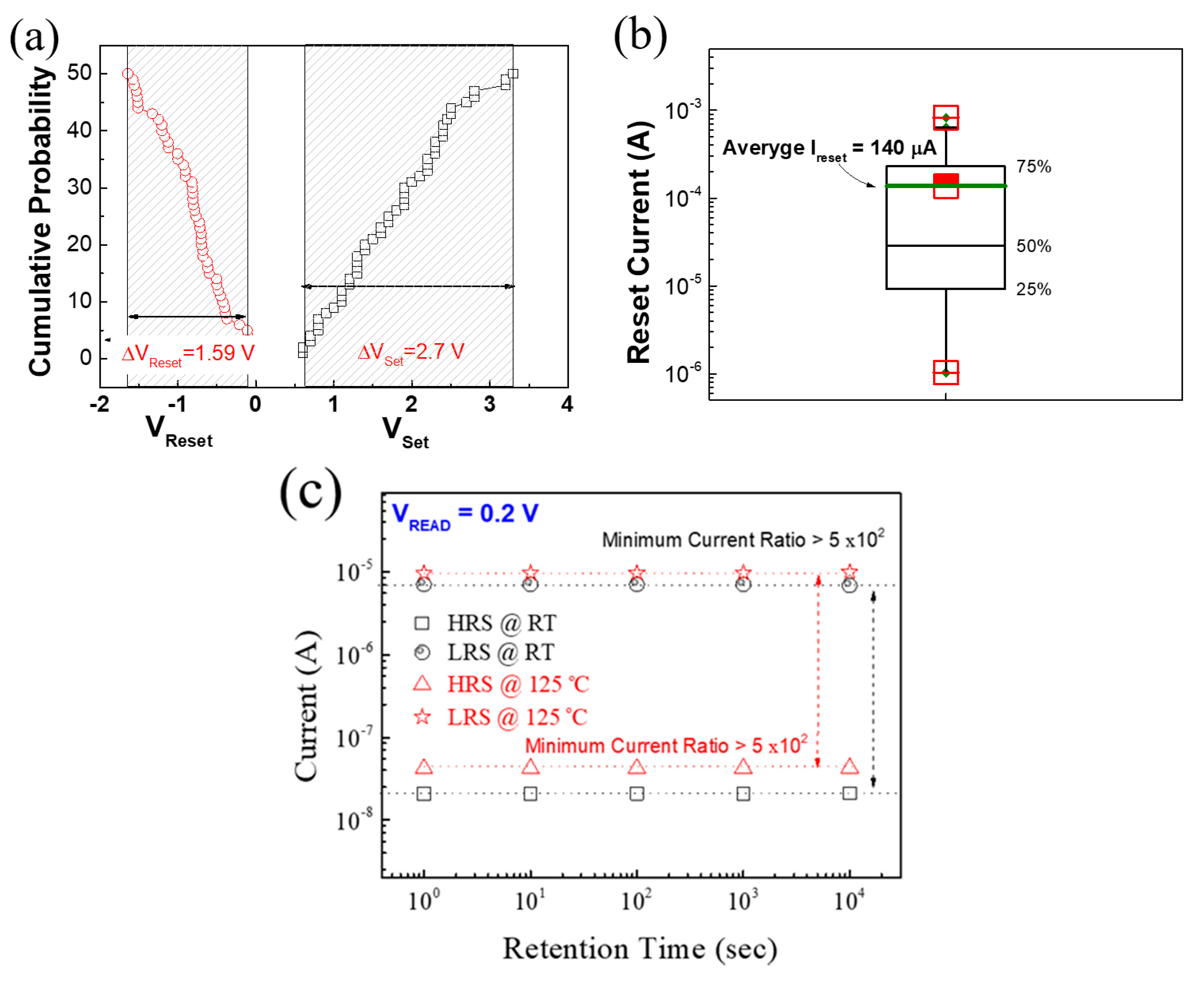
3. Results and Discussion

First, to evaluate a structural property of ZrN films, we investigate XRD peaks for the O-doped ZrN fims using Joint Committee on Powder Diffraction Standards (JCPDS) cards. As shown in Figure 1, it is found that the O-doped ZrN film has a polycrystalline structure for the samples before and after N2 annealing; the measured diffraction peaks were observed at 28°, 30°, 35°, 50°, 53°, and 60°, corresponding to ZrON (222), ZrN (111), Zr (002), ZrN (220), Zr (110), and Zr (103) planes [13,14], in the scanned range of 20°–80°. In the case of as-deposited films, we found several Zr metal peaks as well as those related to ZrN and ZrON, which means that the film might be very leaky when bias is applied to the device. On the other hand, compared to the as-deposited samples, larger diffraction peaks are observed at ~28° and 30° for the O-doped ZrN fims after annealing, which indicates improvement in crystallinity, by removing the Zr related peaks. In addition, to evaluate the crystallinity of O-ZrN films, we tried to calculate the weight fraction of the crystal part using using Hinrichsen’s method [15,16], as shown in inset table of Figure 1b As a result, compared to the crystallinity before RTA, after heat treatment, the crystallinity of ZrN and Zr decreased, while that of ZrON has doubled. These results mean that the post-RTA method is very useful in improving the crystallinity of O-ZrN by reducing the crystallization of Zr and ZrN components.
To investigate the RS properties for the O-doped ZrN RRAM devices with different bottom electrode, i.e., Pt and PtSi, as can be seen in Figure 2a,b, we measured the I–V curve in the dc mode. In the six Pt/O-doped ZrN/TiN cells, memory operation was observed in bipolar RS mode. First, as shown in Figure 2a a forming is required +2.3 V for a bipolar RS with compliance current (Icc), which indicates that the resistance state of the devices is switched to low resistive state (LRS). Then, a reset process was performed at −3 V by sweeping a reverse voltage for the sample, in Figure 2b the resistance state was changed to the high resistive state (HRS). Subsequently, the current abruptly rises near +1.3 V when the forward voltage is applied to the TE, meaning that the memory cell has been switched back to the LRS. In this cell, when using Vread = +0.2 V, current ratio (CR) is ~102 as shown in Figure 2b. Then, to confirm the conduction property of PtSi, we measured the I–V curve characteristics in Figure 2b. As a result, we observed a current level of <100 nA at ±3 V in I–V curve. In addition, when applying PtSi to the bottom electrode, a forming voltage was slightly rose to +3.6 V, while the self-current limiting characteristic was obtained, as shown in Figure 3a. Then, compared to the Pt BE samples, the memory cells with PtSi BE shows slightly higher operating voltage such as Vset and Vreset, but have a lower operating current characteristic, less than two orders. On the other hand, in order to verify the oxygen doping effect, as shown Figure 2a,b, we investigated the PtSi/ZrN/TiN device using un-doped ZrN films. As a result, compared to RS characteristics of the un-doped ZrN film, although the operating voltage is slightly increased, the operating current can be lowered by more than two orders, and the CR has also increased by 10 times. Thus, it can be confirmed that oxygen doping in ZrN films directly affects the reduction of the current level of the device, as well as increase of CR. As a result, the use of PtSi as BE increases the operation voltage slightly, but the memory cells can operate in the nanoampere level, especially the cell’s operation current can be reduced up to two orders, compared to the memory cell with Pt BE, so it is evaluated as a very effective BE.
To further study the conduction properties for PtSi/O doped ZrN/TiN samples, we investigated the fitted I–V curve by using various models such as Ohmic conduction, Fowler–Nordheim tunneling, Schottky emission, direct tunneling, P–F emission, and SCLC, respectively [17,18]. As a result, as shown in the inset of Figure 2a, before the forming process, the RS curve of a pristine device was matched with P–F emission model with ln (I/V) vs. sqrt (V). After the forming process, as shown in Figure 2b, the RS curves at both HRS and LRS were consistent with SCLC model of I~V1 at voltages from 0 V to +1.5 V (ohmic behavior), and I~V2 over +2 V (Child’s Law), respectively. The resistance state then shifted from HRS to LRS at the trap-filled limit voltage (VTFL) of +2.2 V during the set process. In short, in the case of pristine cells, the O-doped ZrN film has a high resistance, in the inset of Figure 2a, and the fitting results were well consistent with P–F emission. On the other hand, after a forming process, the results of SCLC fitting at both HRS and LRS showed that many traps were created during the forming process and could be distributed uniformly under the conduction band. Therefore, the generation and erasing of nitrogen (or oxygen) vacancies can contribute to RS phenomena from high resistance to low resistance, and from low resistance to high resistance, via charge trapping/de-trapping process. Noth that the P–F emission and SCLC models are as one of the bulk-limited conduction mechanisms, which depends on charge trapping and de-trapping in trap sites of the film [19,20,21,22,23].
Then, to evaluate the voltage variations for the proposed PtSi/O-doped ZrN/TiN RRAM, as shown in Figure 3a, distribution characteristics were investigated for the 10 memory cells. In this experiment, each sample performed RS operation five times in bipolar RS mode. Firstly, in Figure 3a, a slight change was observed in the reset operation of ∆1.59 V, while slightly increased voltage variation of 2.7 V was observed, which is still in reasonable operating range. Then, as shown in Figure 3b, we tested the reset current variation on six memory cells. As a result, it is found that most reset operations occurred in the range of 1 µA to 800 µA, with an average reset current of 140 µA. The reset current could also be 1 order lower than when Pt was used as the BE, and the memory cell could be reset in ~µA level, which might be a very meaningful result in terms of device reliability and power consumption.
Finally, to study the reliability of proposed RRAM cell, the retention time at the LRS and HRS were investigated by examining the data storage capacity of the proposed cell, in Figure 3c. In this result, it is revealed that the CR of about 5 × 10² between both the HRS and the LRS stably remains without major changes for ~104 s at 25 °C. In addition, to evaluate the thermal stability of the proposed cell, we conducted for the same time at high temperature (125 °C). As a result, when increasing a temperature, the current value slightly increased at both states, compared to room temperature (RT), while a CR of about 5 × 10² was maintained up to 104 s.

4. Conclusions

In summary, we investigated bipolar resistive switching (RS) properties using oxygen-doped zirconium nitride (O-doped ZrN) films with platinum silicide (PtSi) bottom electrode (BE). As a result, a PtSi/O-doped ZrN/TiN memory cell showed slightly increased foaming voltage, but the operation current could be reduced by about two orders. In addition, in the retention test, the stable memory states with the CR of about 102 were performed at RT.

Author Contributions

Conceptualization, J.J. and H.-D.K.; methodology, H.-D.K.; validation, S.K.; formal analysis, J.J.; investigation, D.B.; data curation, D.B.; writing—original draft preparation, J.J. and H.-D.K.; writing—review and editing, S.K.; supervision, H.-D.K.; project administration, H.-D.K.; funding acquisition, H.-D.K. All authors have read and agreed to the published version of the manuscript.

Funding

This research was supported by Basic Science Research Program through the National Research Foundation of Korea (NRF) funded by the Ministry of Education (no. NRF-2020R1F1A1048423) and by Korea Institute for Advancement of Technology (KIAT) grant funded by the Korea Government (MOTIE) (P0012451, The Competency Development Program for Industry Specialist).

Data Availability Statement

Data sharing is not applicable to this article as no new data were created or analyzed in this study.

Conflicts of Interest

The authors declare no conflict of interest.

References

  1. Yang, J.J.; Pickett, M.D.; Li, X.; Ohlberg, D.A.; Stewart, D.R.; Williams, R.S. Memristive switching mechanism for met-al/oxide/metal nanodevices. Nat. Nanotech. 2008, 3, 429–433. [Google Scholar] [CrossRef] [PubMed]
  2. Han, J.-W.; Ryu, S.-W.; Kim, C.-J.; Kim, S.; Im, M.; Choi, S.-J.; Kim, J.S.; Kim, K.H.; Lee, G.S.; Oh, J.S.; et al. Partially Depleted SONOS FinFET for Unified RAM (URAM)—Unified Function for High-Speed 1T DRAM and Nonvolatile Memory. IEEE Electron Device Lett. 2008, 29, 781–783. [Google Scholar] [CrossRef]
  3. Kim, S.-J.; Park, Y.-S.; Lyu, S.-H.; Lee, J.-S. Nonvolatile nano-floating gate memory devices based on pentacene semiconductors and organic tunneling insulator layers. Appl. Phys. Lett. 2010, 96, 33302. [Google Scholar] [CrossRef]
  4. Kim, J.; Cho, S.; Kim, T.; Park, J.J. Mimicking Synaptic Behaviors with Cross-Point Structured TiOx/TiOy-Based Filamentary RRAM for Neuromorphic Applications. J. Electr. Eng. Technol. 2019, 14, 869–875. [Google Scholar] [CrossRef]
  5. Yang, M.; Wang, H.; Ma, X.; Gao, H.; Wang, B. Effect of nitrogen-accommodation ability of electrodes in SiNx-based resistive switching devices. Appl. Phys. Lett. 2017, 111, 233510. [Google Scholar] [CrossRef]
  6. Saifeddine, C.; Karim, Z.; Lotfi, B.; Atef, K. Microstructure Characterization of an Aluminium Alloy Processed by Milling Followed by Spark Plasma Sintering. Cryst. Res. Technol. 2018, 53, 1700137. [Google Scholar]
  7. Kim, S.; Kim, H.; Jung, S.; Kim, M.-H.; Lee, S.-H.; Cho, S.; Park, B.-G. Tuning resistive switching parameters in Si3N4-based RRAM for three-dimensional vertical resistive memory applications. J. Alloys Compd. 2016, 663, 419–423. [Google Scholar] [CrossRef]
  8. Chen, C.; Yang, Y.C.; Zeng, F.; Pan, F. Bipolar resistive switching in Cu/AlN/Pt nonvolatile memory device. Appl. Phys. Lett. 2010, 97, 083502. [Google Scholar] [CrossRef]
  9. Kim, H.-D.; An, H.-M.; Kim, K.C.; Seo, Y.; Nam, K.-H.; Chung, H.-B.; Lee, E.B.; Kim, T.G. Large resistive-switching phenomena observed in Ag/Si3N4/Al memory cells. Semicond. Sci. Technol. 2010, 25, 065002. [Google Scholar] [CrossRef] [Green Version]
  10. Kim, H.-D.; Yun, M.J.; Kim, T.G. Self-selection bipolar resistive switching phenomena observed in NbON/NbN bilayer for cross-bar array memory applications. Appl. Phys. Lett. 2014, 105, 213510. [Google Scholar] [CrossRef]
  11. Zheng, Q.; Mei, A.B.; Tuteja, M.; SanGiovanni, D.G.; Hultman, L.; Petrov, I.; Greene, J.E.; Cahill, D.G. Phonon and electron contributions to the thermal conductivity of VNx epitaxial layers. Phys. Rev. Mater. 2017, 1, 065002. [Google Scholar] [CrossRef] [Green Version]
  12. Kumar, D.; Chand, U.; Siang, L.W.; Tseng, T.-Y. ZrN-Based Flexible Resistive Switching Memory. IEEE Electron Device Lett. 2020, 41, 705. [Google Scholar] [CrossRef]
  13. Čyvienė, J.; Dudonis, J. Zr, ZrN and Zr/Al Thin Films Deposition Using Arc Evaporation and Annealing. Acta Phys. Pol. A 2008, 114, 769–777. [Google Scholar] [CrossRef]
  14. Kim, H.-D.; An, H.-M.; Sung, Y.-M.; Im, H.; Kim, T.G. Bipolar Resistive-Switching Phenomena and Resistive-Switching Mechanisms Observed in Zirconium Nitride-Based Resistive-Switching Memory Cells. IEEE Trans. Device Mater. Reliab. 2013, 13, 252–257. [Google Scholar] [CrossRef]
  15. Chiu, F.-C. A Review on Conduction Mechanisms in Dielectric Films. Adv. Mater. Sci. Eng. 2014, 2014, 1–18. [Google Scholar] [CrossRef] [Green Version]
  16. Lim, E.W.; Ismail, R. Conduction Mechanism of Valence Change Resistive Switching Memory: A Survey. Electronics 2015, 4, 586–613. [Google Scholar] [CrossRef]
  17. Nath, R.; Perlman, M. Effect of crystallinity on charge storage in polypropylene and polyethylene. IEEE Trans. Electr. Insul. 1989, 24, 409–412. [Google Scholar] [CrossRef]
  18. Boukezzi, L.; Boubakeur, A.; Lallouani, M. Effect of artificial thermal aging on the crystallinity of XLPE insulation cables: X-ray study. In Proceedings of the 2007 Annual Report-Conference on Electrical Insulation and Dielectric Phenomena, Vancouver, BC, Canada, 14–17 October 2007; IEEE: Piscataway, NJ, USA, 2007; pp. 65–68. [Google Scholar]
  19. Oh, S.-I.; Rani, J.R.; Hong, S.-M.; Jang, J.-H. Self-rectifying bipolar resistive switching memory based on an iron oxide and graphene oxide hybrid. Nanoscale 2017, 9, 15314–15322. [Google Scholar] [CrossRef]
  20. Bang, S.; Kim, M.-H.; Kim, T.-H.; Lee, D.K.; Kim, S.; Cho, S.; Park, B.-G. Gradual switching and self-rectifying characteristics of Cu/α-IGZO/p+-Si RRAM for synaptic device application. Solid-State Electron. 2018, 150, 60–65. [Google Scholar] [CrossRef]
  21. Kim, H.-D.; Kim, S.; Yun, M.J. Self-rectifying resistive switching behavior observed in Al2O3-based resistive switching memory devices with p-AlGaN semiconductor bottom electrode. J. Alloys Compd. 2018, 742, 822–827. [Google Scholar] [CrossRef]
  22. Zhang, Z.; Gao, B.; Fang, Z.; Wang, X.; Tang, Y.; Sohn, J.; Wong, H.-S.P.; Wong, S.S.; Lo, G.-Q. All-Metal-Nitride RRAM Devices. IEEE Electron Device Lett. 2014, 36, 29–31. [Google Scholar] [CrossRef]
  23. Fu, Y.; Huang, C.-C.; Wang, J.-C. Nonlinear resistive switching features of rapid-thermal-annealed aluminum nitride dielectrics with modified charge trapping behaviors. Microelectron. Eng. 2019, 216, 111033. [Google Scholar] [CrossRef]
Figure 1. (a) (left side) Device schematic diagram of PtSi/ O-doped ZrNx/TiN RRAM cell and manufacturing procedure. (B) (right side) Cross-sectional image and top view of fabricated device measured by FE-SEM. (b) X-ray diffraction (XRD) curves measured for O-ZrN films annealed in the scan range of 20°–80°. Inset table shows crystallinity of ZrN, Zr, and ZrON using Hinrichsen’s method.
Coatings 11 00197 g001
Figure 2. (a) Forming process and (b) resistive switching characteristics in current-voltage curve characteristics at room temperature for the PtSi, Pt/O-doped ZrN/TiN, PtSi/O-doped ZrN/TiN and PtSi/ZrN/TiN samples. Inset of Figure 2a shows P–F fitting with ln (I/V) vs. sqrt (V) for forming curves and (c) SCLC fitting with log-log scales in I–V curves.
Coatings 11 00197 g002aCoatings 11 00197 g002b
Figure 3. Analysis of (a) the set/reset voltage variations and (b) the current variations for the PtSi/O-doped ZrN/TiN RRAM cells. (c) Retention properties for the devices with active size of 150 × 150 µm2 at 0.2 V in the LRS and HRS for 104 s at 25 °C.
Coatings 11 00197 g003
Publisher’s Note: MDPI stays neutral with regard to jurisdictional claims in published maps and institutional affiliations.

