
Adaptive Control of Photovoltaic Systems Based on Dual Active Bridge Converters


1
Departamento de Mecatrónica y Electromecánica, Instituto Tecnológico Metropolitano, Medellín 050036, Colombia
2
Facultad de Minas, Universidad Nacional de Colombia, Medellín 050041, Colombia
*
Author to whom correspondence should be addressed.
Computation 2022, 10(6), 89; https://0-doi-org.brum.beds.ac.uk/10.3390/computation10060089
Submission received: 4 May 2022
/
Revised: 24 May 2022
/
Accepted: 25 May 2022
/
Published: 1 June 2022
(This article belongs to the Section Computational Engineering)
Abstract
:Dual active bridge converters (DAB) are used to interconnect photovoltaic (PV) generators with AC and DC buses or isolated loads. However, a controller is needed to provide a stable and efficient operation of the DAB converter when the PV generator must be interconnected with a DC bus, which is particularly important in microinverter applications. Therefore, this paper proposes the design of a cascade controller for a PV system based on a DAB converter. The converter is controlled using a peak current control and an adaptive PI voltage control; thus the methodology to design the cascade controller is developed in two steps; first, the PV system formed by a PV generator, a DAB converter, and an inverter or load is introduced, including the description of the leakage current; as a second step, the model of the PV system to design the cascade controller is presented. Then, a relationship between the phase shift factor and the peak current of the leakage inductor is derived, which is used to design the peak current controller to ensure the DAB converter operation at the most efficient operating condition. On the other hand, an adaptive PI controller for the PV voltage is designed to ensure the reference tracking provided by a maximum power point (MPP) algorithm. The effectiveness of the proposed cascade controller is demonstrated through realistic examples simulated in PSIM. The power and control circuits implemented in PSIM are presented to encourage the use of the proposed solution. The simulation results confirm the correct operation of the control system, which mitigates the oscillatory perturbation produced by an inverter connected to the PV system, and also ensures the maximum power extraction from the PV panel by following the MPP reference.
1. Introduction
In recent decades, the generation of electrical power has been based on fossil and nonrenewable fuels, causing a negative impact on the environment. Efforts are being made to include into the energy matrix renewable sources with a lower impact on the environment. Photovoltaic (PV) systems are a renewable option that has gained the most attraction in recent years [1,2].
PV systems are interconnected in electrical networks called microgrids, which are a group of distributed generators, energy storage elements, and loads connected together, coordinated by a central control system [3]. There are three types of microgrids based on the nature of the current generated: direct current (DC), alternating current (AC), and hybrid, which includes both types of currents. Each type has one or more connected nodes called buses, where sources, loads, and storage systems converge. In the case of PV systems, DC/DC converters must be used to interface the PV generator with the DC bus of a DC or hybrid microgrid; for AC microgrids, a DC/AC converter interfaces the PV system with the AC bus [4].
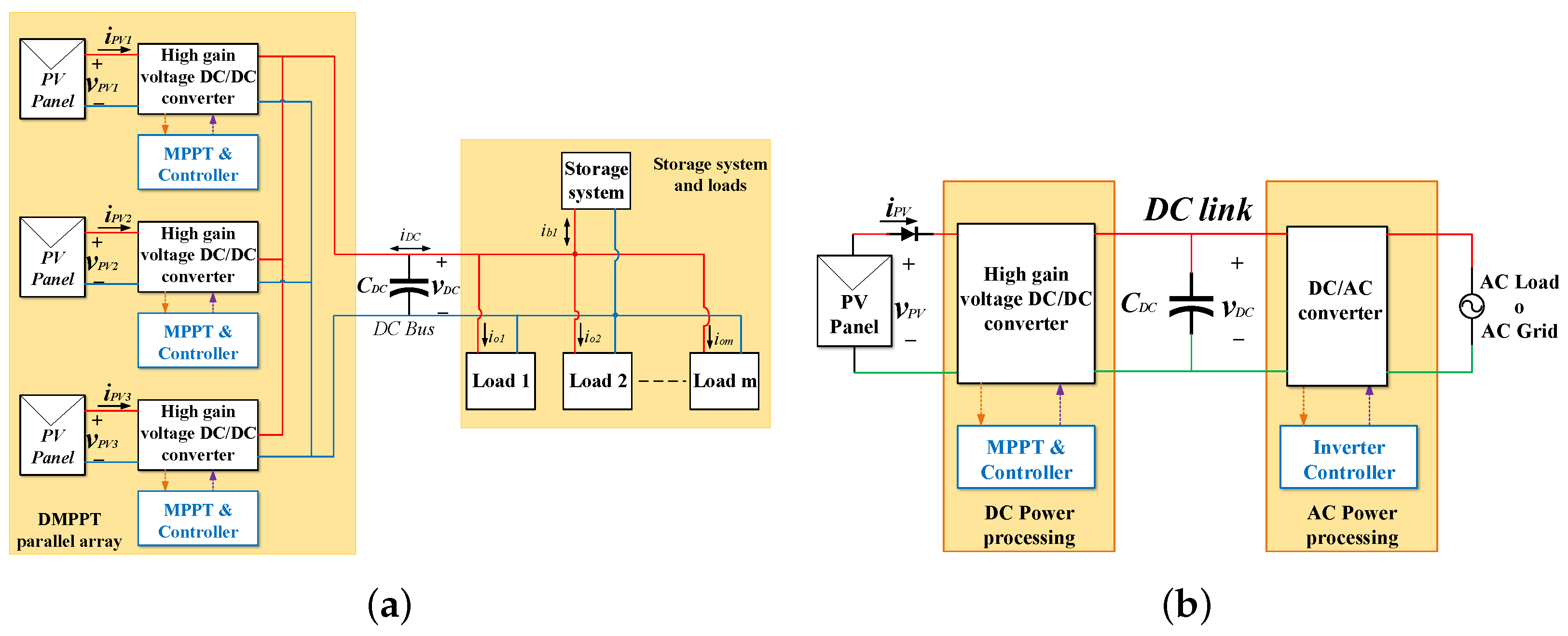
Photovoltaic systems formed by series and/or parallel connections of PV modules are known as PV arrays. Such a system can be affected by a phenomenon called mismatching [5], which is caused by manufacturing differences, environmental conditions, partial shading by nearby or distant objects, and nonuniform operating conditions, among other sources. A large part of energy losses in PV arrays are associated with the mismatching phenomenon; therefore, different solutions have been proposed, which are organized into three groups based on the maximum power point tracking (MPPT) architecture [6]: centralized MPPT architecture (CMPPT), distributed MPPT architecture (DMPPT), and reconfiguration of the modules in a PV array (RMPPT). The DMPPT solution is presented as the most promising alternative to generate the maximum electrical energy, but its main drawback is the high number of converters needed to process the electric power [7]. The DMPPT array could be series or parallel connected; the parallel option is presented in Figure 1a, which requires converters with high voltage gain, but it offers more reliability since the operation of each set of PV panel and converter does not depend on the other sets. Instead, in a series connection, the failure of one converter could degrade the operation of the sets in the array [8].
In DC microgrids based on parallel DMPPT, such as the one depicted in Figure 1a, the DC/DC converters interfacing the PV panels must be regulated to guarantee a stable operation and to track the maximum power point (MPP) of the PV panel. In the case of AC microgrids based on parallel DMPPT, it is necessary to use microinverters formed by DC/DC and DC/AC converters to deliver power to the grid or to the AC load, as depicted in Figure 1b.
The structure of Figure 1 shows that a DC/DC converter with high gain voltage and a robust controller is needed for DMPPT parallel solutions; thus, multiple approaches have been presented in the literature. Concerning DC/DC converter topologies, the cascaded boost converter has been widely used due the construction simplicity, voltage boost capability, and low current ripple at the panel side. However, the higher the voltage gain, the lower the efficiency [9,10]. Other solutions have been based on the cascade connection of nonisolated and low-voltage converters, where the efficiency is compromised since the converters are added in cascade [11]. Moreover, nonisolated topologies with high-voltage gain have been used in [12] featuring an interleaving structure. Furthermore, a combination of buck and boost classical converter topologies, as those presented in [13,14], are used to obtain a quadratic gain voltage. Multiport DC/DC converters are used in [15] to interface three sources and to reach a high-voltage gain. In addition, there are approaches that use self-coupled inductors to reach a high-voltage gain [16,17], but the main drawback of those solutions is the high number of elements, which affects the system reliability [11].
In the case of isolated DC/DC converters, different topologies have been used [18,19], which can be designed to achieve high-voltage gain due to the use of transformers. In those converters, the voltage and current stress on the semiconductors and passive elements must be limited, otherwise the converter efficiency could be severely reduced. However, the galvanic isolation provided by these converters is a useful feature in PV systems, since it decouples the grounds from the panels and loads, thus increasing the safety of the PV system. Within the isolated topologies, the growing interest in the double active bridge (DAB) converter is highlighted in [20]: such a converter provides galvanic isolation, high-voltage gain, and a soft switching capability [21], which reduces the stress on the semiconductors. Moreover, the DAB converter provides high efficiency even with high-voltage gains [22].
Because of the benefits provided by the DAB converter, this work is focused on the use of such a converter for PV systems. However, it is needed to develop a controller for the DAB converter designed to follow the reference provided by an MPPT system, which is needed to maximize the power production. Different control strategies applied to the DAB converter are found in the literature; for example, the work presented in [23] is intended for battery charging in electric vehicles, where cascade PI control strategies are used to regulate both the input an battery current. In [24], a multi-input DAB converter is used, with ultracapacitor and battery connections, to regulate the DC bus voltage in a microgrid based on renewable energy systems; in such a work the converter is controlled using both voltage and current PI regulators. Similarly, the work reported in [25] presents a solid state transformer based on a multi-input DAB converter, where a PV panel is interfaced with a boost converter to reach the MPP, while a battery is used to regulate the DC bus voltage by controlling the phase shift with a PI controller; this controller is similar to the solution presented in [26]. Furthermore, a microinverter for the PV panel and battery interface is proposed in [27], which is based on a modified DAB converter with two inputs for a PV panel and a battery bank; in this case, the adopted PI controllers are intended to reach the MPP of the PV panel, to compensate the 100 Hz–120 Hz perturbation in the DC link, and to regulate the AC current of the inverter; a similar work is presented in [28], though intended for standalone applications. For general purpose applications, the work reported in [29] uses a cascade PI controller to regulate both the power flow and the output voltage. On the other hand, a battery charging/discharging application is presented in [30], where a double-integral sliding-mode controller is designed to regulate the battery current and the DC bus voltage. Other application is reported in [31], where a fuzzy-logic controller is designed to regulate the DC bus voltage of a DC microgrid based on a DAB converter. The control strategies for DAB converters reported in the literature include PI controllers, sliding mode control, fuzzy logic, and a linear quadratic regulator (LQR), among others; the advantages and disadvantages of those DAB controllers are summarized and discussed in [32].
A general purpose control strategy for the DAB converter was reported in [33], which consists of a programmed current controller. In such a controller, the transformer current is monitored and the semiconductors are switched based on a hysteresis band, which is defined according to the control objective. This current controller guarantees the correct operation of the converter since it avoids transformer saturation. In [33], a proportional voltage control is added, in cascade, with the programmed current controller and a feed-forward loop, which is designed to reduce the steady-state error and to provide a fast dynamic response. However, that work does not present a method for selecting the proportional constant, and the desired dynamic behavior is not ensured for different operating points, which is important for PV systems, since the operating point changes with the solar irradiance. For the particular use of DAB converters in PV applications, the work reported in [34] presented a particle swarm optimization to perform the MPPT action and to control the DAB converter by defining the phase shift factor. In addition, the work reported in [35] presented a control-oriented model of the PV system, demonstrating the model usefulness by designing PID controllers for the PV current and voltage. Nevertheless, the control systems discussed before do not ensure the same dynamic response for different operating points; therefore, the system performance and stability is not ensured for the whole operating range.
Taking into account the high voltage conversion ratio and high efficiency of the DAB converter, which make it suitable to interface PV panels with electric grids or AC loads, this work proposes a cascade controller formed by a peak current control and an adaptive PI control, which is designed to ensure the correct and safe operation of a PV system based on a DAB converter. In this solution, the peak current controller changes the phase shift factor as a function of the peak current in the leakage inductor of the high frequency transformer (HFT). This controller ensures a zero DC current to avoid the transformer core saturation, which enables a stable and efficient operation of the PV system. The adaptive PI controller adjusts its parameters according to the operating point to guarantee a stable operation; this adaptive controller also defines the peak current reference to ensure the same dynamic behavior of the PV voltage, for the entire operating range, which is necessary to follow the reference delivered by an MPPT algorithm guaranteeing maximum power extraction. The solution presented in this paper mitigates the main disturbances of a PV system formed by a PV panel, a DAB converter, and a grid-connected inverter.
The rest of the paper is organized as follows: Section 2 describes the DAB-based PV system, and the operation of that PV system is analyzed in detail. Then, Section 3 presents the mathematical model of the system, which is focused on the relationship between the panel voltage and the leakage inductor current of the converter transformer. Section 4 shows the design of both the peak current controller and the adaptive voltage control. The proposed solution is validated in Section 5, which presents the design procedure of the control system and the results obtained in an application case. Finally, the conclusions close the paper in Section 6.
2. PV System Based on the DAB Converter
This work is focused on designing a controller for PV systems based on the DAB converter, hence the operation of such a system must be analyzed.
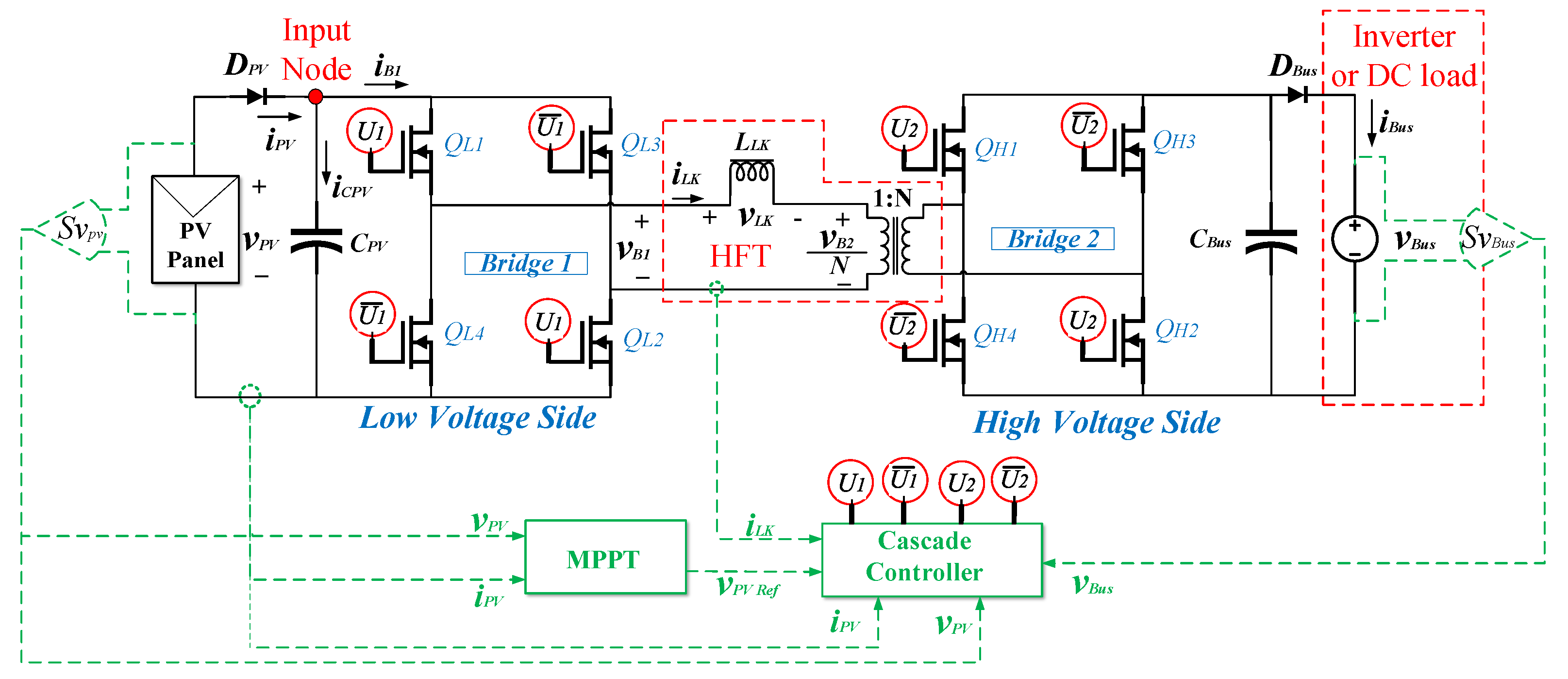
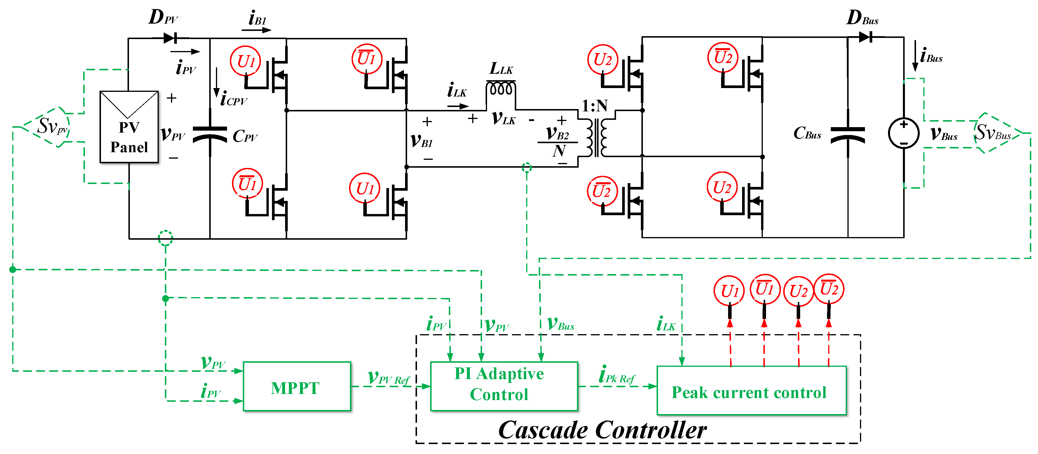
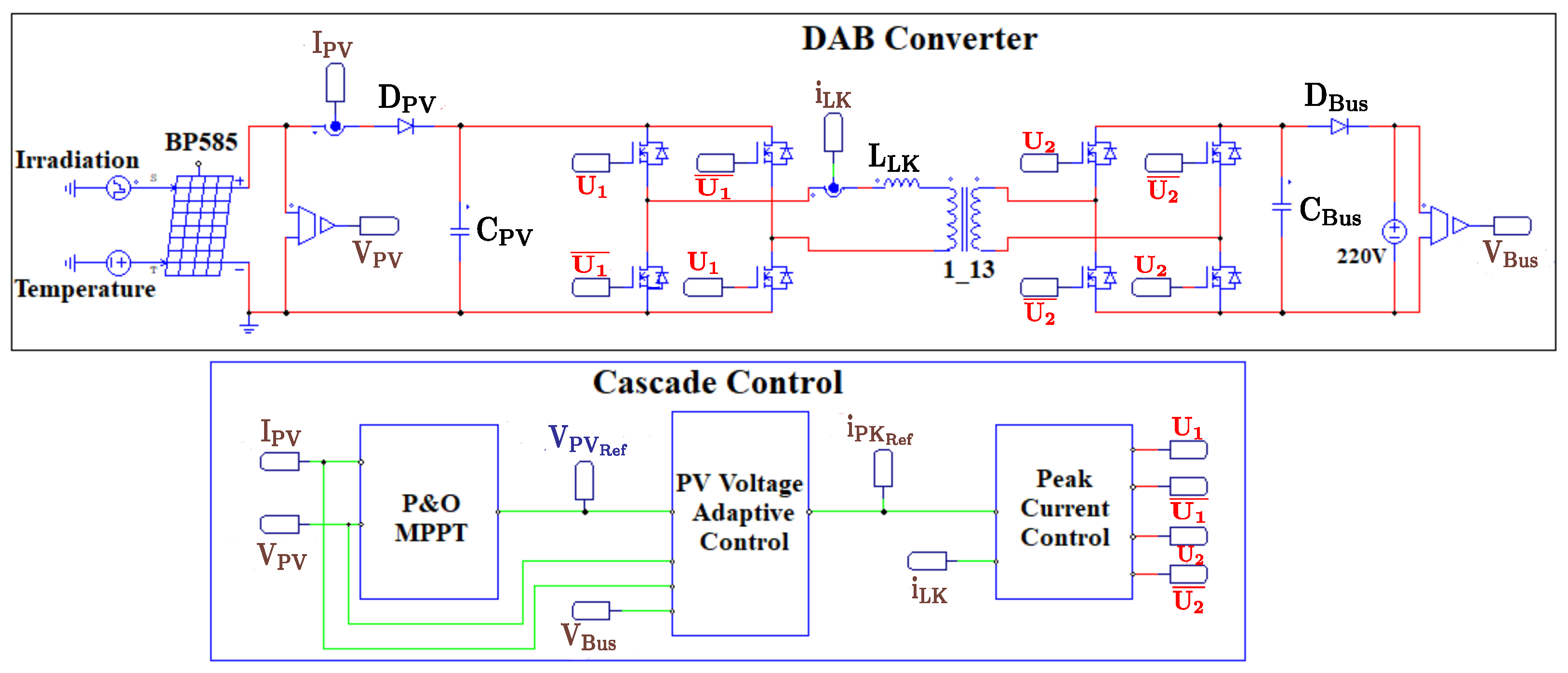
The electrical scheme of a PV system based on the DAB converter is presented in Figure 2. In such a system, the PV panel is connected to the input of the low-voltage side of the DAB converter, and the output of the high-voltage side is connected to a voltage source , which models the interaction with a grid-connected inverter or a DC load. Since the DAB converter is a bidirectional topology, two diodes, and , are placed at the input and output of the converter, respectively, to prevent current flow from the DC bus to the PV panel.
The capacitor is inserted between the PV panel and the converter to filter the current ripple generated by the low-voltage bridge of the DAB converter. Similarly, the capacitor is needed to filter the current ripple generated by the high-voltage bridge of the DAB converter, thus avoiding the propagation of high-frequency harmonics into the DC bus. The transistors to form the Bridge 1 (low voltage side) and are driven by the switching signal and its complement . Transistors to form the Bridge 2 (high voltage side) and are commutated using signal and its complement . A high-frequency transformer (HFT) is used to connect both bridges, and its model takes into account the leakage inductance referred to the primary side of a transformer with turn-ratio 1:N. The HFT input voltage is the Bridge 1 voltage , and the HFT output voltage is the Bridge 2 voltage , which can be reflected to the primary side as .
This converter is modulated using the single phase shift (SPS) technique, which consists of generating two digital switching signals ( and ) with a fixed duty cycle (), and a phase shift between and , which is manipulated to regulate the power flow [21,36]. The phase shift factor can take values between −1 and 1, but to transfer power from the PV panel to the DC bus, i.e., unidirectional operation, must be restricted between 0 and 1. In addition, the work reported in [21,36] demonstrated that the higher efficiency for this type of PV system occurs for values between 0 and 0.5. Therefore, the digital signal can change from a low state to a high state only if the digital signal is in a high state; on the contrary, can change from a high state to a low state only if is in a low state.
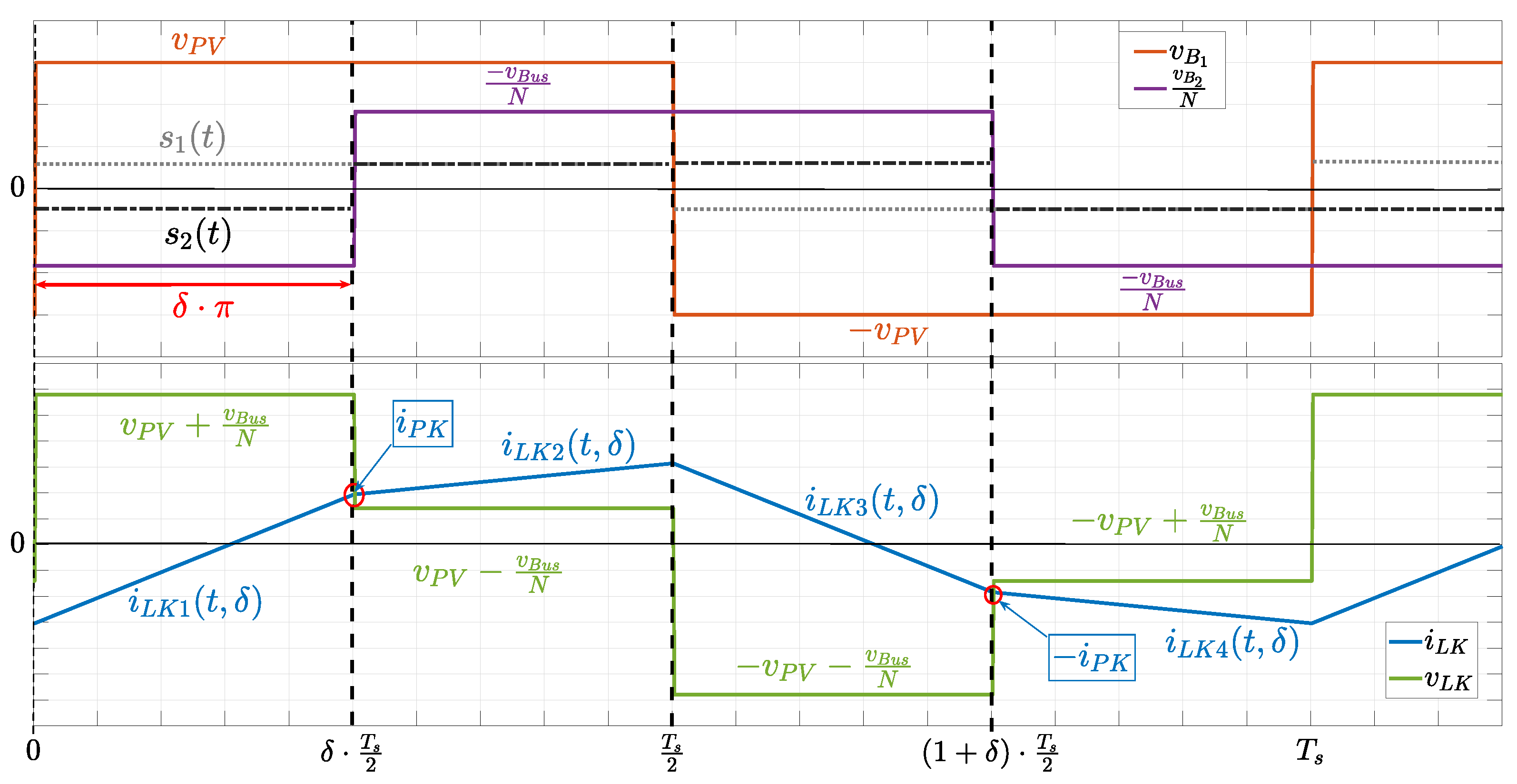
The voltage waveform at the leakage inductor is shown in Figure 3 (green waveform), which is calculated as a difference between bridges voltage (red waveform) and (purple waveform). Those two voltages are phase-shifted by radians in each switching period , which is a consequence of the switching functions and described in (1) and (2), respectively.
Therefore and are described in (3) and (4), respectively, where is the voltage of the PV panel, i.e., at the input of the converter:
On the other hand, the leakage inductor current is also shown in Figure 3, and its waveform is described in (5)–(9) for a switching period. Those equations are obtained from the leakage inductor voltage , and taking into account that . Such expressions also show the relationship between the input and the output voltage of the converter with the current, and the influence of and over are also evident:
3. Model of the PV System
The PV system based on the DAB converter, previously shown in Figure 2, is controlled by changing the phase shift between the switching signals of the bridges. Such a phase shift affects the behavior of and ; therefore, the following subsections analyze those variables. First, the analysis of is presented to define the peak current and its relation with the phase shift factor . Then, the dynamic relation between the PV voltage and is presented, which will be used to design the controller for the PV system.
3.1. Analysis of Peak Current
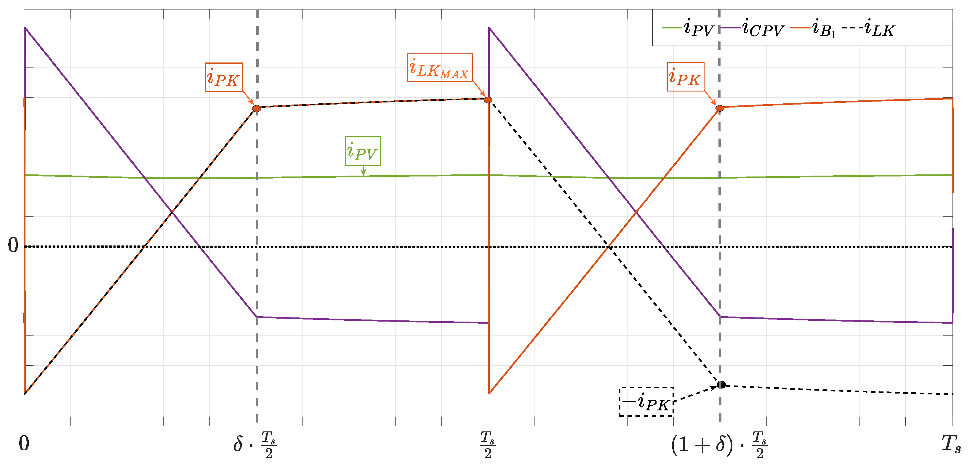
The peak current of is defined by [33] as the current value at the time , because this is the highest value of when is equal or lower than . On the other hand, when is higher than , the highest current value occurs at . In any case, at the time , there is a slope change of as a consequence of the phase shift, thus value is the interest variable to understand the effect of the phase shift over the other variables in the system. Therefore, to model the relation between and , it is necessary to analyze the input node of the PV system, which is highlighted in Figure 2.
Figure 4 shows the currents at the input node, i.e., current , the PV current , and the input current of the Bridge 1 . Moreover, the figure also shows , which evidenced that , given in (10), is equal to for half of the period; for the other half of the period is equal to . In the same figure, it is also observed that is almost constant because absorbs the ripple of ; thus, the DAB converter guarantees a continuous current at the input port. This means that the average values of and are equal; thus, manipulating the value enables the controller to modify the average of , which also modifies the PV current. Therefore, can be used to change the operating point of the PV panel to track the MPP.
The value of for these systems was calculated in [36], and it is reported in Equation (11), where the relation between the phase shift factor and the value of and is observed. This expression can also be interpreted as follows: having the values of , , , and N constant, it is possible to change the phase shift between the switching signals of the DAB bridges by imposing a particular peak current on the leakage inductor or a particular PV panel voltage, which in turns defines the power flow from the PV source to the load.
3.2. Analysis of Relation between and
Applying Kirchoff’s current law on the input node of the PV system leads to Equation (12), which relates the dynamic behavior of the average value with the changes on the average values of and . The average value of the Bridge 1 current is calculated from expression (10) following the PV current analysis reported in [36], which leads to the value given in (13):
Therefore, replacing (13) into (12) leads to the expression for the dynamic behavior of given in (14), which depends on , PV average current , bus average voltage , and the parameters of the system. Finally, expression (14) shows that the PV voltage can be regulated by acting on the phase shift factor:
On the other hand, solving (11) for results in expression (15). Then, replacing such a value into (14) leads to (16), which describes the dynamic behavior of as a function of . Thus, such a dynamic expression can be used to design a PV voltage controller in which is the manipulated variable. Therefore, an additional controller is needed.
4. PV System Control Design
The operating point of PV panels must be regulated to maximize the power production. This regulation process requires two main components: an MPPT algorithm providing the reference of the MPP, and a voltage controller to ensure a stable operation at the MPP.
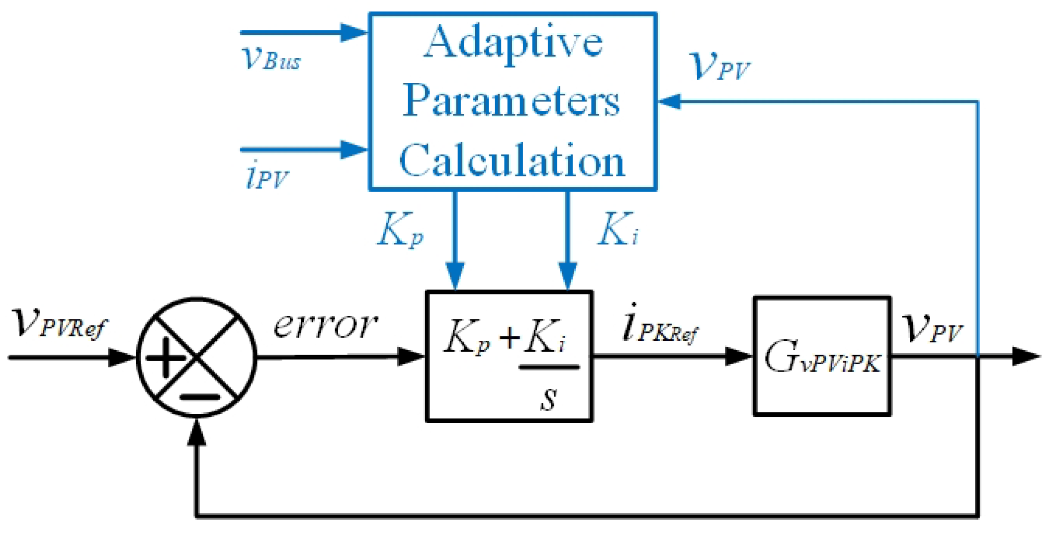
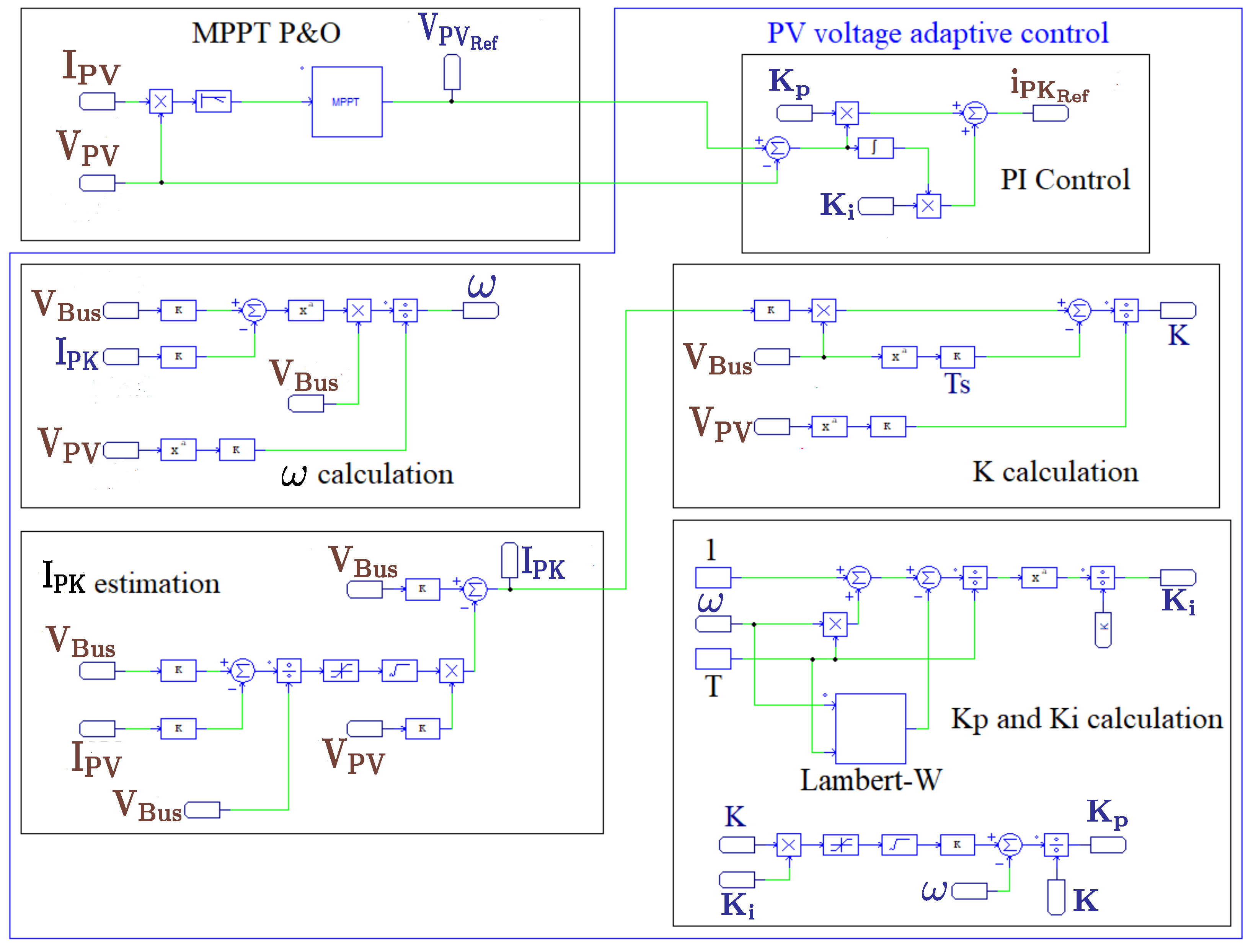
This section presents the design of a cascade controller to regulate a PV system based on a DAB converter. The control structure is depicted in Figure 5, where the PV voltage is regulated using an adaptive PI controller, which provides the reference for a peak current controller (also known as programmed current controller). Figure 5 shows the DAB converter and the PV panel (solid black line) with relevant variables. The connection between the cascade controller and the MPPT block (solid green line) shows the variables measured in the PV-DAB system (dotted green lines): the inputs of the controller are the PV current and voltage, the bus voltage, and the leakage current; the outputs of the controller are the switching signals for the converter transistors (red dotted lines). The following subsections describe in detail the design of both the current and voltage control loops.
4.1. Design of the Current Controller
The DAB converter has an HFT to a high voltage conversion ratio and galvanic isolation; however, it is necessary to ensure that both the primary and secondary sides of the HFT have zero DC current to avoid core saturation. This is the reason to impose a duty cycle for each bridge of the converter.
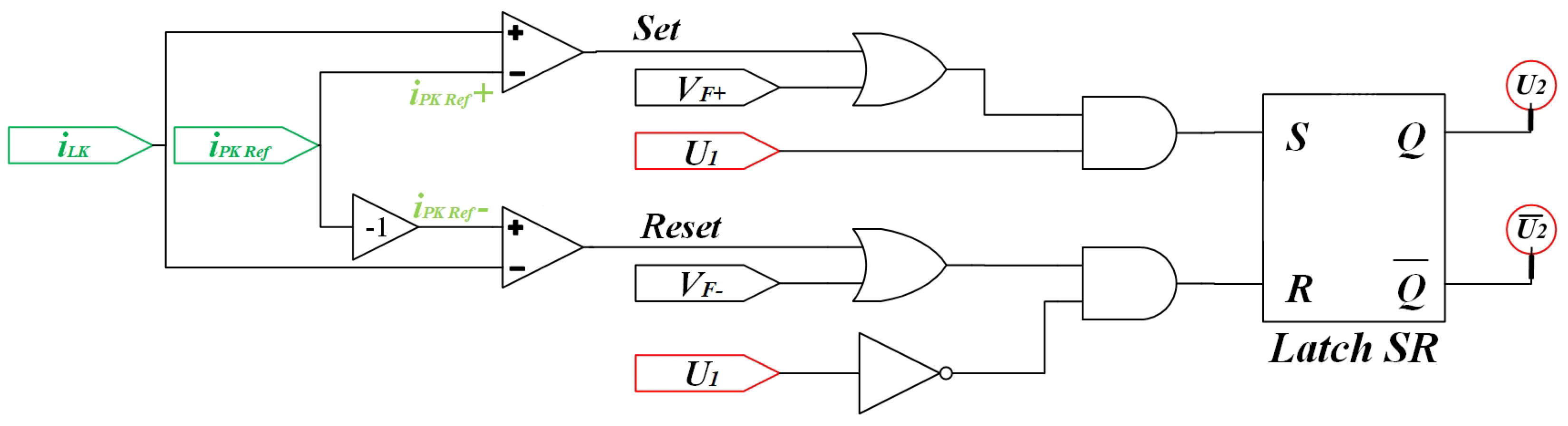
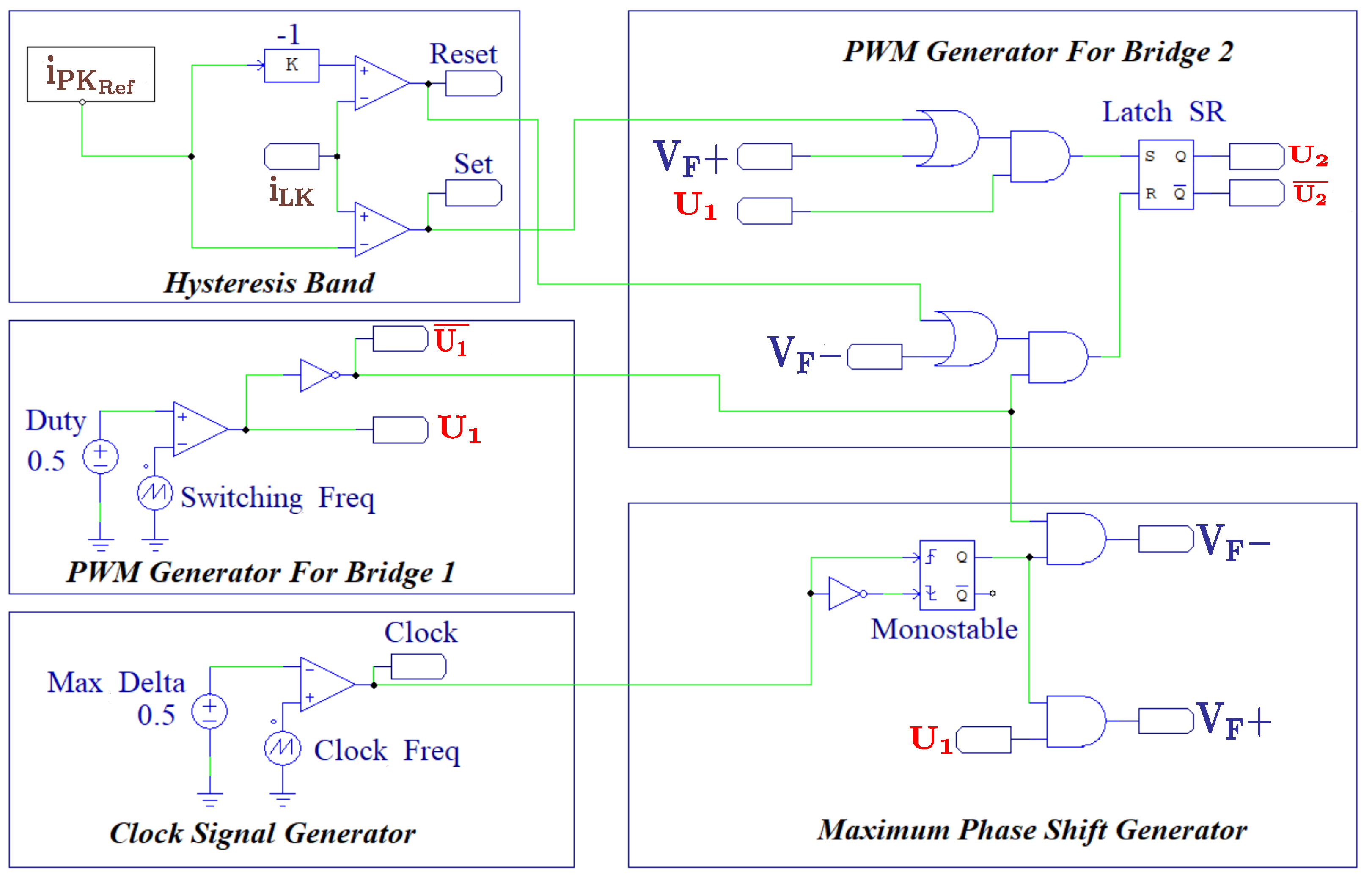
The zero DC current condition is ensured by adopting the double band current control reported in [33], which consists of a hysteresis band that guarantees the same magnitude of at instants and (with negative sign): from Figure 4, it is observed that such a condition forces is symmetrical with respect to zero, thus imposing a zero DC current in the HFT.
The peak current control is in charge of defining the phase shift between the PWM signal driving the Bridge 1 and the PWM signal driving the Bridge 2 . Given that both and have a duty cycle, the signal will change from low to high when is high and the desired value (upper limit of the hysteresis band ) has been reached. Similarly, for the other part of the period, will change from high to low when is low and the desired value (lower limit of the hysteresis band ) has been reached. Figure 6 shows the circuit designed to detect the instants in which the desired values are reached, which is based on a comparator circuit with hysteresis. Such a circuit compares with the limits and , which are equal in magnitude but with opposite signs. Then, two comparators generate a when , and generates a when .
The work reported in [36] demonstrated that the maximum phase shift factor, for a DAB-based PV system, should be to ensure the operation at the highest efficiency region of the converter. Therefore, it is necessary to include such a limitation into the peak current control. This is done in the circuit of Figure 6 by using the digital variables and , which inform to the circuit if the maximum phase shift has been reached. In consequence, a change from high to low in is forced when is activated; on the other hand, if is activated, a change from low to high in is generated. Such a condition is imposed with OR gates between the Set/Reset and / signals, respectively. Finally, the control signal of the second bridge is set to only when , and it is reset to only when to fulfill the restrictions of SPS and high efficiency operation [20,21,36]. The previous control behavior is formalized in the control law described in (17):
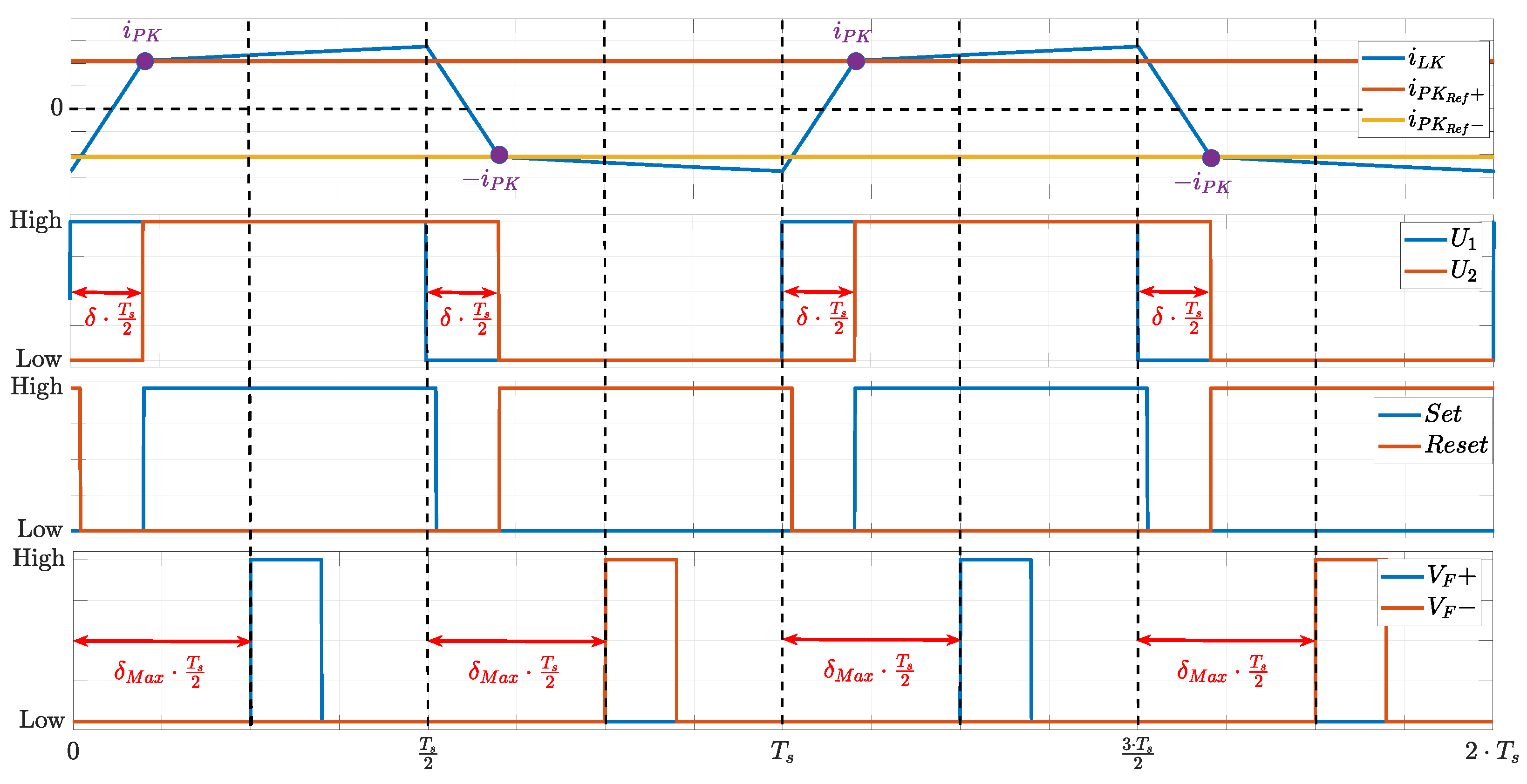
The steady-state behavior of the previous control law is illustrated in Figure 7 and Figure 8 for the two possible conditions: reaching the hysteresis limits and reaching the maximum phase shift, respectively. Figure 7 shows that reaching the upper value of the hysteresis band () forces the signal to be activated before the maximum phase shift value is reached, which in turn triggers the change of signal from low to high. Similarly, when reaches the lower value of the hysteresis band (), the signal is activated before the maximum phase shift value signal, thus forcing the signal to change from a high to low state.
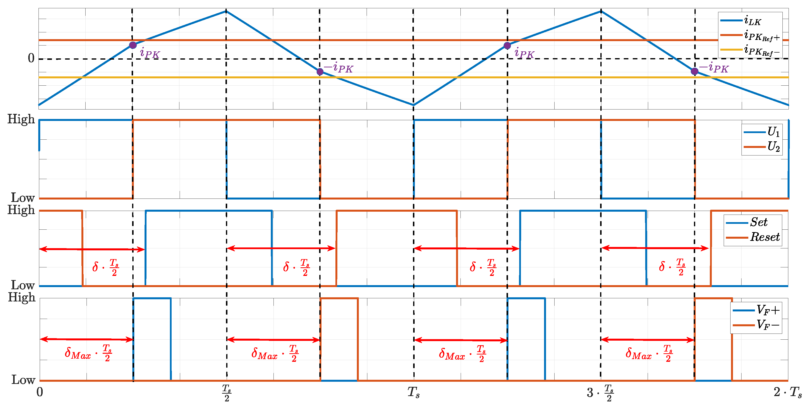
On the other hand, Figure 8 shows the case where the maximum phase shift signal is activated before the signal, which forces the change of the signal from low to high because has not reached the upper value of the hysteresis band. Similarly, when the signal is activated before the signal, i.e., has not reached the lower value of the hysteresis band, the signal is forced to change from high to low. This process ensures a maximum phase shift lower than 0.5, thus ensuring the operation of the DAB converter in the maximum efficiency zone.
In conclusion, this current controller guarantees the following conditions:
- The value does not exceed the positive and negative values defined by the hysteresis band.
- The average value of is equal to zero, thus avoiding core saturation in the HFT.
- The phase shift is lower than 0.5, thus ensuring an efficient operation of the DAB converter.
Finally, a cascade PV voltage controller, which defines the reference of the current controller, is required to impose the desired operating point to the PV system.
4.2. Design of an Adaptive PI Control of
In this work, the control of is performed by acting on . For this purpose, an adaptive PI controller is proposed, in which the proportional and integral parameters of the controller are continuously updated depending on the operating point of the system, thus guaranteeing a stable operation with the desired dynamic behavior.
To design the adaptive PI control, Equation (16) is used to obtain a small-signal model around an arbitrary operating point using the perturbation and linearization technique [37], which leads to the small-signal model reported in Equation (18). In such an expression, and represent the small-signal variations of the PV panel voltage and the peak current of , respectively. The variables , , and represent the operating point of the system. Moreover, in steady state, Equation (16) is equal to zero, thus solving it for enables to estimate the steady-state value of given in (19):
The transfer function between and is obtained from Equation (18) and reported in Equation (20). Such a relation is a first-order transfer function, where its gain K is reported in (21) which is negative if or positive on the contrary. Moreover, the variable, presented in Equation (22), is the magnitude of the transfer function pole; it is observed that as long as and are positive, then will be positive, thus the pole will be located on the left side of the complex plane. Such a condition guarantees that represents a stable relation between the PV panel voltage and the peak current of the leakage inductor.
The control scheme for the PV panel voltage is presented in Figure 9, where the transfer function represents the PV system with the peak current control. The PI controller acts based on the error signal and delivers the peak current reference to , as shown in (23). However, and parameters are updated, in real time, as depicted in Figure 9.
The closed-loop transfer function of the system presented in Figure 9 is reported in Equation (24). Based on the denominator of the canonical form of a second-order system [38], the parameters and are rewritten in terms of the damping factor and natural frequency as given in (25) and (26), respectively. In PV systems, there should not be overshoot in the dynamic response of , since voltage overshoots will move away the PV voltage from the optimal operating condition defined by the MPPT algorithm. Such a null overshoot condition is guaranteed by selecting . On the other hand, the selection of depends on the desired settling time T, which must be shorter than the perturbation time of the MPPT algorithm. This condition is needed to ensure the stability of the MPPT as described in [39,40].
Then, solving from (26) leads to Equation (27). Similarly, using to solve Equation (25) provides the expression given in (28), which requires the value of , it can be observed that if K is negative then and must be negative in order for the system to be globally stable. Then, replacing Equation (28) into (24) provides the transfer function given in Equation (29):
The controller is designed taking into account a Perturb & Observe (P&O) algorithm for the MPPT action [39,40]. The P&O algorithm changes the reference of the PV voltage in steps with amplitude each seconds. Therefore, the step response of the PV panel voltage must be analyzed; such a PV voltage waveform , in Laplace domain, is given in (30). Then, using the inverse Laplace transformation, the step response of in time domain is reported in (31):
The settling time T of the PV voltage (31) is calculated when , where is the band most commonly adopted. Then, is calculated by solving Equation (32), which provides the value given in Equation (33), where is the lambert-W function:
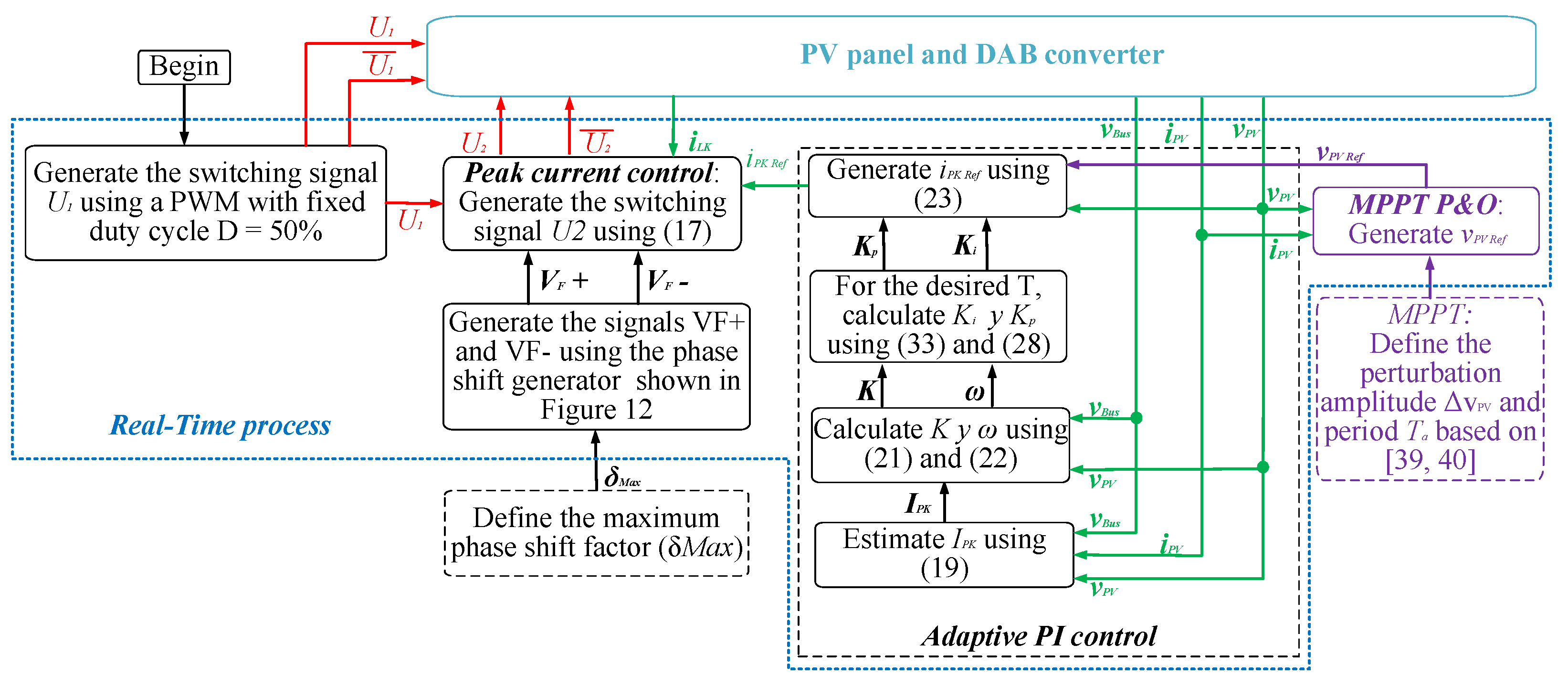
To synthesize the implementation of the proposed control system, an operation diagram of the complete control system is presented in Figure 10, in which the main equations of the control process are highlighted. In addition, the switching signals are indicated in red color, the measured variables are indicated in green color, and the calculated parameters are presented in black color. Moreover, the process related to the MPPT P&O algorithm is highlighted in purple color, and the process that runs continuously, in real time, is highlighted in a blue box.
Finally, Table 1 shows a summary of the comparison between the proposed adaptive control system (named Proposed) and two different solutions, highlighting the controlled variables, the damping factor, the high-efficiency operation capability, the operation with zero DC current on the HFT, the stability analysis, the possibility to reach the MPP of the PV panel, and the rejection of DC bus disturbances. Taking into account that the control of PV systems based on the DAB converter is a recent research topic, there are few contributions. The control system presented in [34] is focused on improving the MPPT of the system, but that work does not present the controller design; therefore, some control parameters are not analyzed. Similarly, the solution reported in [35] shows the design of two independent PI controllers, one of them controls and the other one controls . Such a control design is based on the linearization of the system model around an operating point; therefore, the dynamic response of the closed-loop system is not guaranteed over the entire operating range, but the PV system can reach the MPP under steady-state conditions. Table 1 reports that the controller in [34] regulates the PV voltage but any stability analysis or performance criteria is taken into account, only the MPP tracking is discussed. On the other hand, the controller presented in [35] regulates the PV voltage or current, while the damping factor is not ensured; such a work ensured the operation at the high efficiency condition, but no stability analysis of zero DC current is provided. Finally, the proposed solution provides a defined damping factor and, at the same time, ensures the operation at the high efficiency condition with zero DC current, this even under sinusoidal disturbances caused by the grid connection.
5. Circuital Implementation and Application Example
The proposed control system for a PV system based on the DAB converter was validated using the power electronics simulator PSIM [41]. Such a professional simulator takes into account the nonlinear behavior of the semiconductors (MOSFETs and diodes), the effect of the HFT leakage inductor, and the nonlinear model of a commercial PV panel, which in this case corresponds to the BP585 [42].
For this application example, the design of the DAB converter was performed following the procedure presented in [36]; the resulting parameters of the converter, the PV panel, and the DC bus are reported in Table 2.
The implementation of the PV system in PSIM is depicted in Figure 11, where the nonlinear elements are observed. In addition, such an electrical scheme also shows the control blocks, which will be described and validated in the following subsections.
5.1. Implementation of the Peak Current Controller
The peak current controller was implemented based on the schematic presented in Figure 6. Figure 12 shows the PSIM implementation of the peak current controller, which is formed by multiple blocks, each one of them dealing with a particular function.
The block PWM Generator For Bridge 1 has a classical PWM structure, and it produces the switching signal and its complement with a frequency of 50 kHz and a duty cycle of . The maximum phase shift factor is calculated with a clock signal, generated by the block Clock Signal Generator, which produces a clock signal with a duty cycle of and a frequency equal to the double of the switching frequency; thus, the clock signal changes each , i.e., the maximum to operate at the maximum efficiency region of the converter [36]. Then, the Maximum Phase Shift Generator block takes the clock signal and generates a pulse whenever there is a rising edge using a monostable circuit, which feeds two AND gates. One of those gates produces the signal if the maximum is reached while , and the other gate produces the signal if the maximum is reached while , i.e., . Finally, the blocks Hysteresis Band and PWM Generator for Bridge 2 are the same digital circuit previously reported in Figure 6 and explained in Section 4.1.
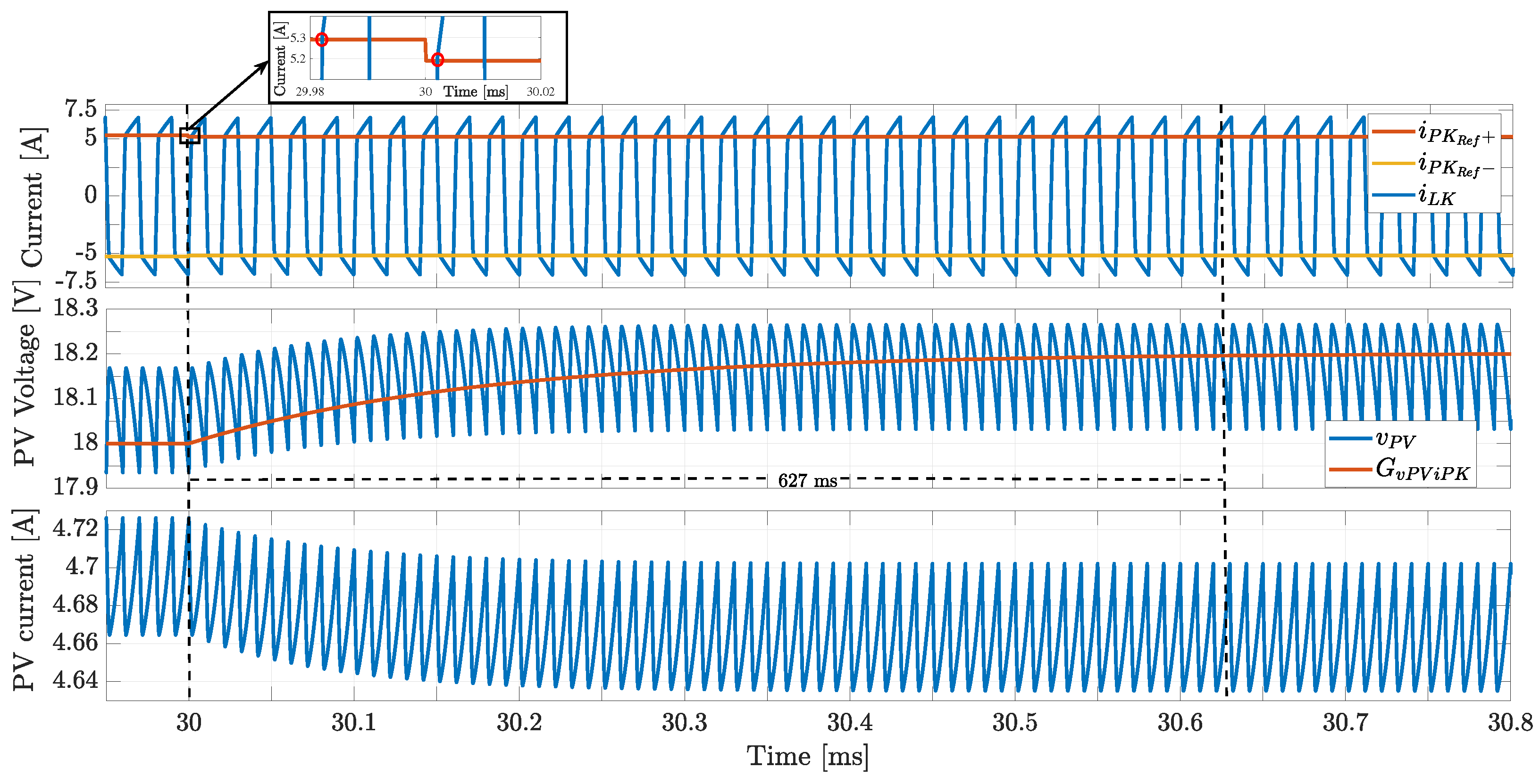
Figure 13 shows the electrical simulation of the PV system under the action of the peak current controller. In this first simulation, the PV system starts the operation with 5.3 A as reference for the value, which sets the average PV voltage to V and the average PV current to A; the figure also shows the waveform of for such a condition. Then, at ms, a change A to A is performed in , thus changing both upper and lower limits of the hysteresis band.
The simulation reports the small-signal response of to the step change in , which is correctly predicted by the small-signal model given by the transfer function shown in (20). Therefore, this simulation confirms that the small-signal model is useful to design the cascade PV voltage controller; thus, it is also confirmed the global stability of the system. In this way, the PV system reaches a steady-state behavior at s, in which the PV voltage is equal to V and the PV current is A. Moreover, the simulation confirms that the peak current controller imposes a symmetrical waveform of in ; hence, the average current is zero, which avoids the HFT saturation to ensure the desired operation of the PV system.
5.2. Implementation of the Adaptive PV Voltage Controller
The implementation of the voltage controller requires the real-time calculation of the PI parameters and , which is performed in the block and calculation, described in Figure 14, using Equations (28) and (33).
This verification example considers a settling time ms with a band V, which was selected based on the perturbation time ms of the algorithm calculated with the procedure reported in [39,40]. In addition, the calculation of requires to compute the Lambert-W function in real time; thus, the formula presented in [43] is implemented in PSIM, which provides a calculation error in the order of .
Moreover, the calculation of and also requires the real-time calculation of the small-signal parameters K and , which is performed in the blocks K calculation and calculation of Figure 14. Those calculations are performed using Equations (21) and (22), but those expressions require the value, which is difficult to measure since changes when the maximum is achieved. Therefore, the control system implementation estimates using Equation (19), which corresponds to the block estimation of Figure 14. Finally, using the previous electrical circuits, the PI parameters are continuously adapted to the operations conditions present in the PV system.
Figure 14 shows the implementation of the PI structure in the block PI Control, which also calculates the error between the PV voltage and the reference value provided by the P&O algorithm; the output of the PI structure is the reference for the peak current controller. Finally, the reference for voltage controller is generated by the algorithm shown in the block MPPT P&O, which was implemented using C code following the guidelines given in [39]: perturbation amplitude V and perturbation period ms.
The blue block PV Voltage Adaptive Control corresponds to the complete adaptive process, which requires the measurement of the PV voltage , the average of DC bus voltage , and the PV current , which is similar to the electrical measurements required by traditional control solutions for PV systems like the ones reported in [9,33,44].
5.3. Performance of the Complete Control System
Multiple tests were performed to validate the proposed cascade connection of the adaptive voltage controller and peak current controller:
- Evaluate the settling time of the PV voltage to changes on the reference value ;
- Evaluate the robustness of the PV voltage controller to perturbations on the bus voltage ;
- Evaluate the performance of the PV voltage under the action of the MPPT () algorithm.
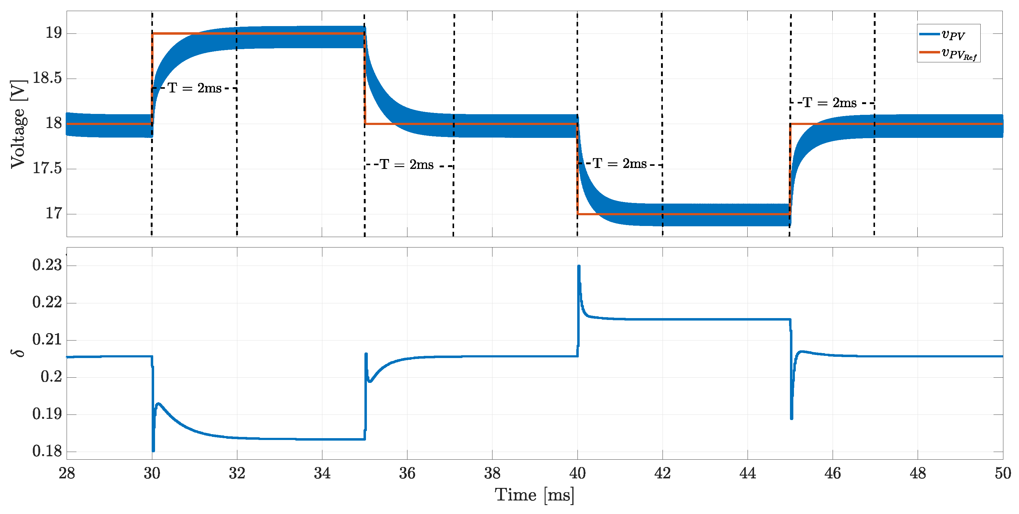
The first test considers step changes on the reference , which have an amplitude of V to be in agreement with the parameter designed for the P&O algorithm. This test was carried out to verify the dynamic behavior imposed by the adaptive PI controller at different operating points, where the settling time is particularly important since the stability of the P&O algorithm depends on that characteristic. The results of this circuital simulation are presented in Figure 15, where the reference changes between V, V, and V in intervals of ms, while the DC bus voltage and irradiances are constant at V and W/m, respectively. For each reference change, the PV voltage shows the desired dynamic behavior: a settling time equal to ms and no overshoot (). The simulation also reports the behavior of the phase shift , which always remains between 0 and . Therefore, high-efficiency operation of the DAB converter is ensured.
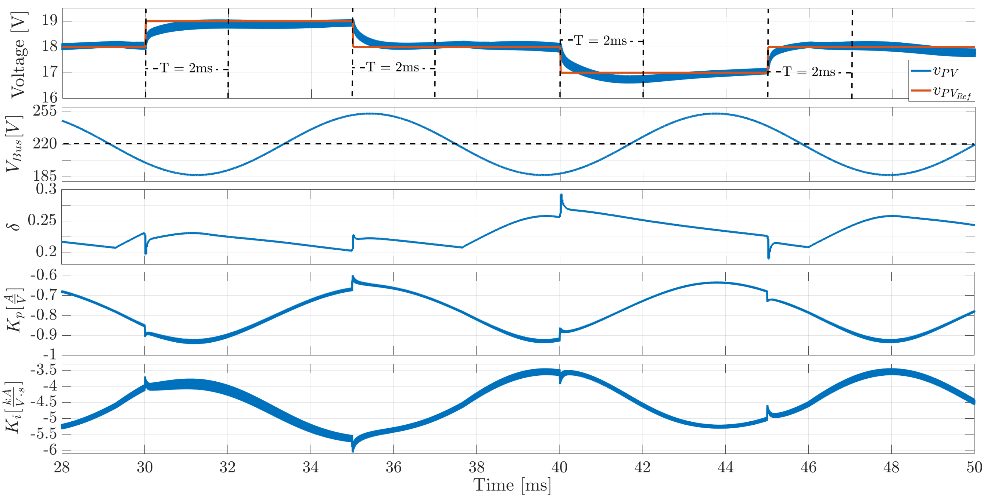
The second test considers the same changes on the reference signal, but a sinusoidal disturbance of V at Hz is added to the DC bus voltage (V), which corresponds to a 30% perturbation. This type of disturbance is typically found in the DC bus of a microinverter [39]. Figure 16 presents the circuital simulation results of this test, where the PV voltage follows the reference with a settling time of ms and a value within 0 and , despite the presence of a large perturbation in the bus voltage. Moreover, the simulation results also report the parameters and , which are continuously adapted to compensate the change on the operating point caused by the perturbations on , thus ensuring the desired behavior under realistic conditions, e.g., a microinverter application.
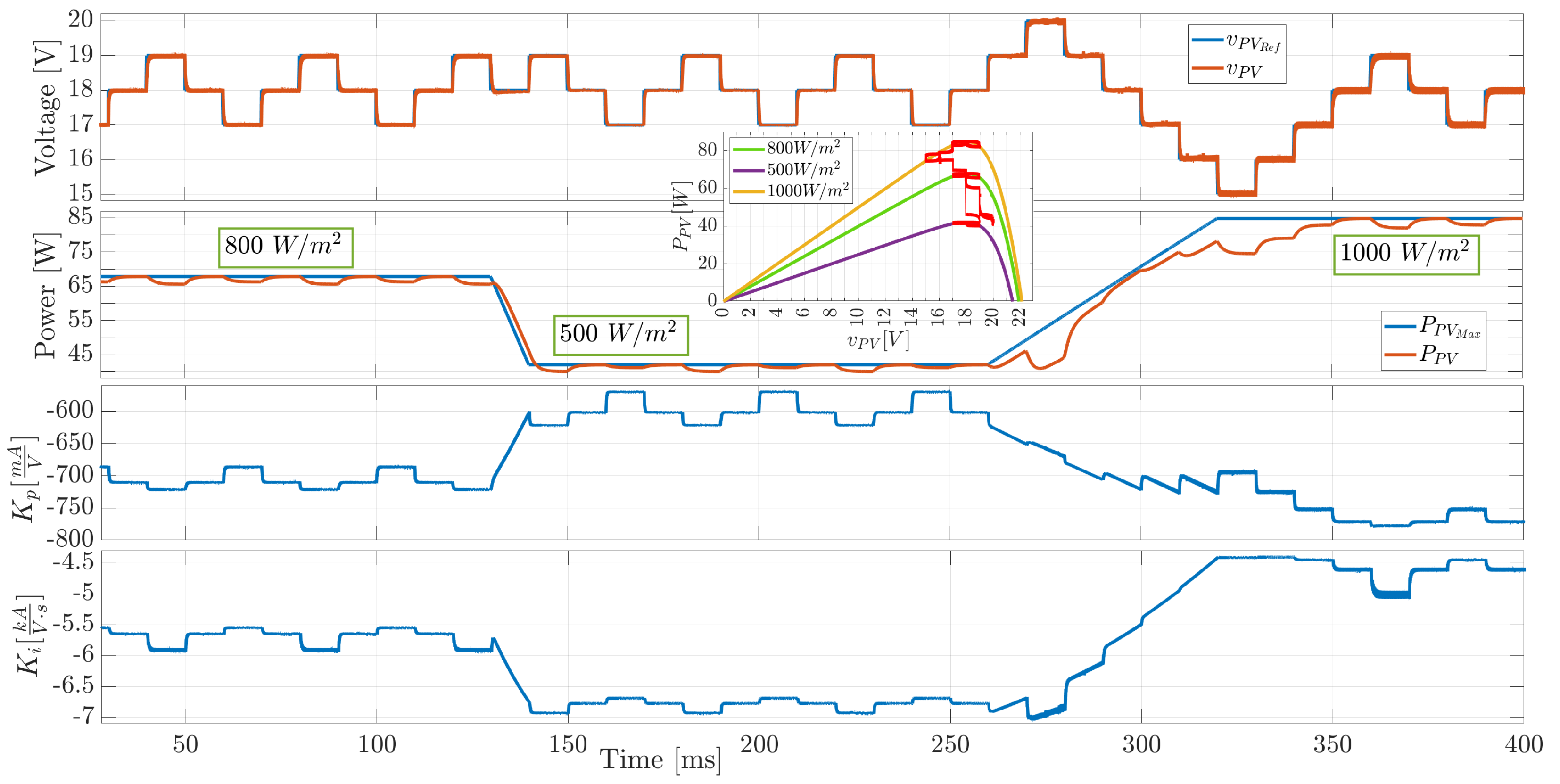
The third test considers the action of the P&O MPPT algorithm, which allows the validation of the proposed controller in realistic conditions. For this test, the irradiance changes between W/m, W/m, and W/m, which forces the P&O algorithm to track the corresponding optimal references for the PV voltage. Figure 17 shows results of this circuital simulation, where the PV voltage always follows the reference provided by the P&O algorithm. Figure 17 also shows the power-vs-voltage curves of the PV module for the three irradiance conditions, and the path followed by the PV system is highlighted in a red trace: the PV system travels from the MPP of the first condition W/m to the MPP of the second condition W/m, then the system travels to the MPP of the third condition W/m; therefore, such a simulation confirms that the highest PV power is always extracted.
The results also confirm that for each irradiance, the PV system reaches the MPP with a tracking time lower than ms and operates with stable behavior, always ensuring a settling time equal to ms. The stable operation of the P&O algorithm is also evident from the three-point behavior of the PV voltage around the MPP, which is the stable operation waveform demonstrated in [39] for a P&O algorithm. Figure 17 also shows the adaptation of the and parameters, where each operating point forces the controller parameters to be recalculated; thus, the PI controller is adapted to impose the desired dynamics in . It should be noted that the simulation shows both the maximum power available for each irradiance condition , and the power extracted from the panel as a consequence of the control system operation is also observed. Those results put into evidence the correct operation of the PV system, since the PV panel always reaches the MPP for any operating point.
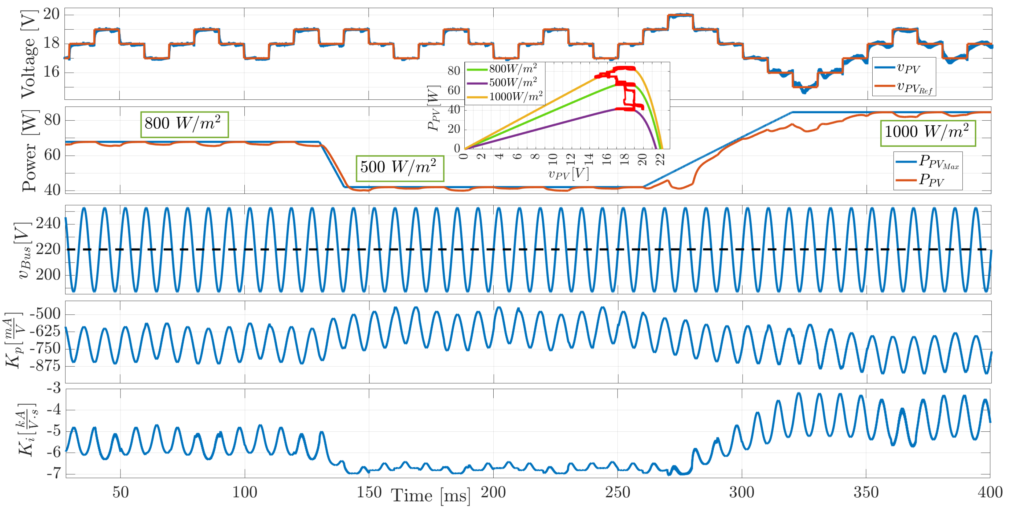
The previous simulation was repeated but including a sinusoidal disturbance of V at Hz in the DC bus. This final condition corresponds to a realistic operation in a microinverter with MPPT capabilities. The results of this last circuital simulations are reported in Figure 18, where the PV panel voltage follows the reference generated by the MPPT algorithm despite the disturbance introduced in . It is also observed the adaptation of and parameters to changes on both the irradiance and the bus voltage, thus ensuring the stability of the PV system. Finally, the path followed by the PV system in the power-vs-voltage curves confirms that the highest PV power is always extracted. Therefore, the previous simulations validate the adaptive control system proposed in this paper.
The next validation is to evaluate the performance of each component of the PV system. The efficiency of a PV panel is calculated as the ratio between the incident solar power and the electric output power. Such an efficiency depends on the materials used in the construction process; for example, Ref. [45] reported efficiencies between (organic cells) up to (Gallium-Arsenic cells). At the commercial level, monocrystalline and polycrystalline cells have a market presence with efficiencies ranging from to [46].
The efficiency of the DAB converter () can be calculated using expression (34), where is the power provided by the PV panel and corresponds to the power losses on the converter. is calculated using expression (35) as reported in [32], where is the equivalent series resistance of and and are the on resistance of the MOSFETs in Bridge 1 and Bridge 2, respectively:
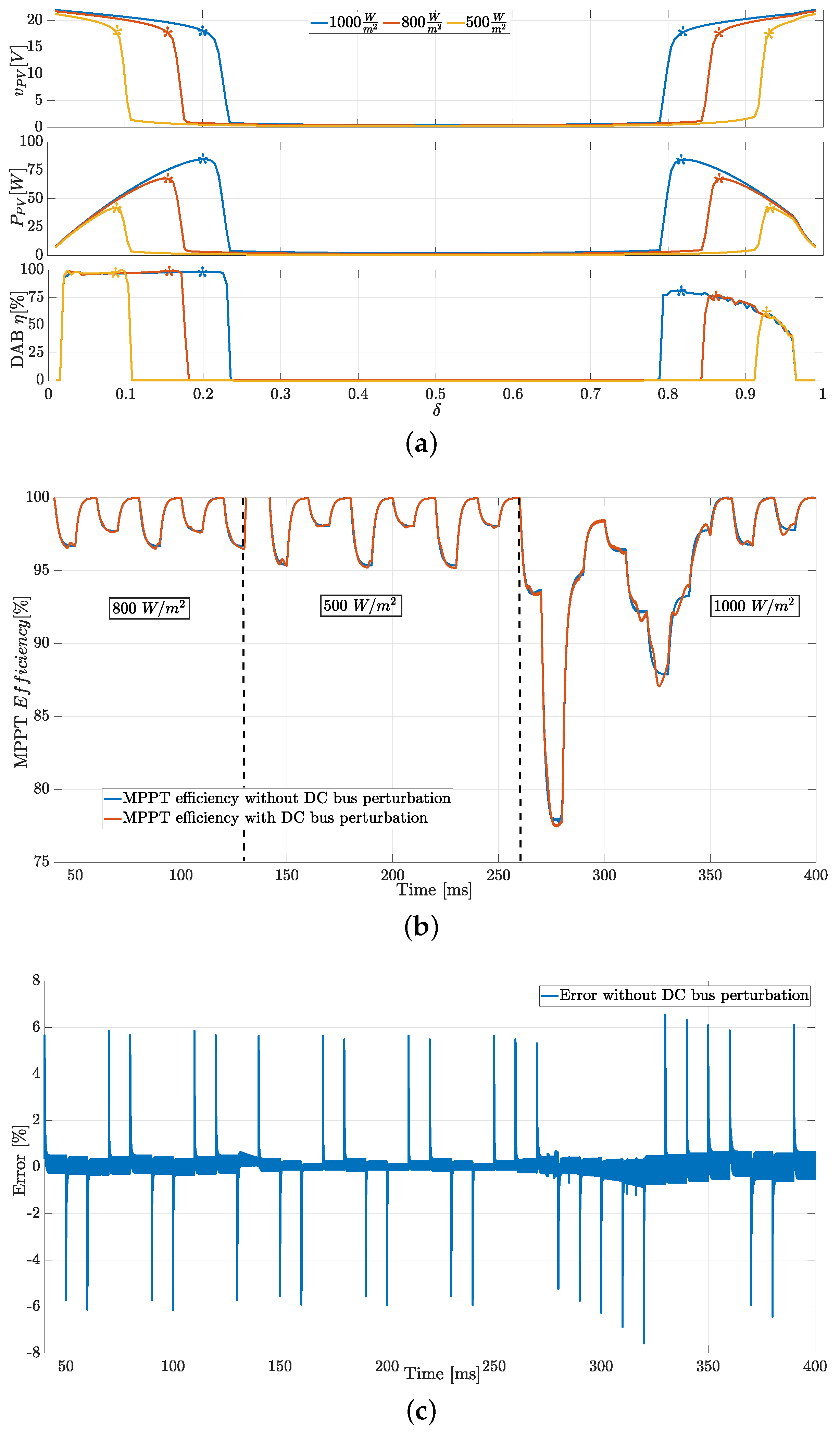
The efficiency of the DAB converter, designed in this application example, is illustrated in Figure 19a as function of for three different irradiances (W/m, W/m, and W/m), and the values of , , and were taken from [32]. The results show that the MPP of the PV panel, for each irradiance, can be reached with two different values; however, the efficiency of the converter is higher for , which was discussed in Section 2, and it is guaranteed by the controller proposed in this work. The efficiency of the DAB converter can be improved by using semiconductors, passive elements, and transformers with lower parasitic resistances.
Another component of the PV system is the MPPT algorithm. The efficiency of the algorithm is measured as the ratio between the power extracted from the PV panel () and the power at the MPP (); hence, it is calculated as . Figure 19b shows the efficiency of the MPPT algorithm for different irradiance conditions, reporting efficiencies higher than and an accuracy of in steady-state operation with and without the presence of Hz sinusoidal perturbations caused by the grid connection. The lowest efficiency is reached when a fast irradiance increment occurs, which is the case after ms, but it is compensated in less than ms. The power ripple of the MPPT is also a performance measure, which in this case is lower than W as reported in Figure 17 and Figure 18. The efficiency and the power ripple of the MPPT can be enhanced by using more efficient algorithms, but the control system proposed in this paper will remain the same.
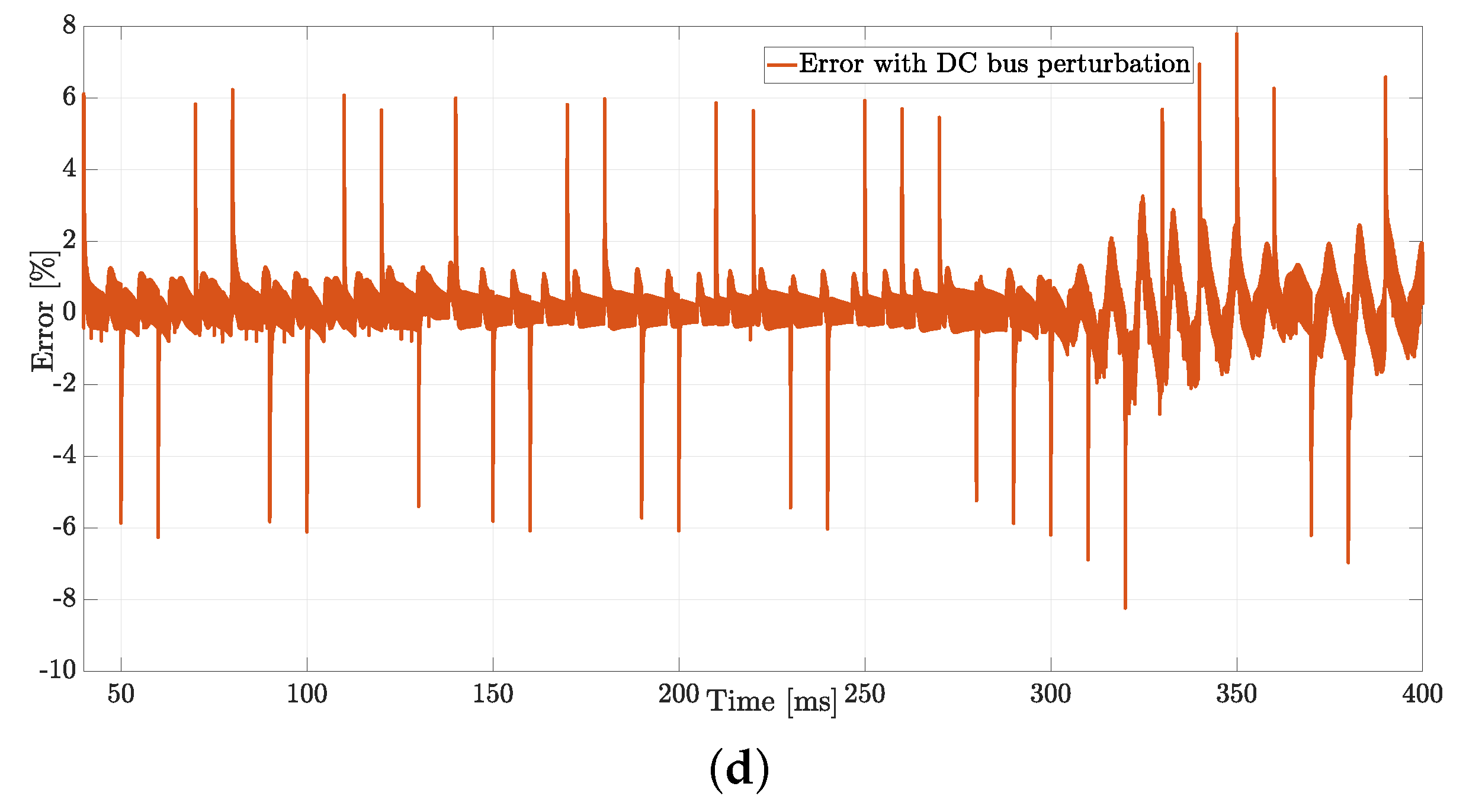
The controller performance is estimated based on the error between the PV voltage () and the reference value () provided by the MPPT algorithm. The error signals for this application example are reported in Figure 19c,d for the operation with and without perturbations at Hz, respectively. The error has a magnitude lower than in steady-state operation; this error exhibits short peaks of when a change in the reference is imposed by the MPPT algorithm each ms. In presence of a fast change in the irradiance value, e.g., after ms, the error is increased ( without 120 Hz perturbations and with those perturbations), but such an error will be reduced when the MPPT controller reaches the MPP condition. This error can be decreased by reducing the PV panel voltage ripple, which can be done by using a larger capacitor.
Finally, the performance of the whole PV system proposed in this work is a combination of the performance of each component previously discussed.
6. Conclusions
A cascade controller, formed by a peak current control and an adaptive PI control of the PV voltage, was designed and validated in this paper. The effectiveness of the cascade controller in the regulation of the PV voltage was demonstrated for a system based on the DAB converter, improving the dynamic response, and ensuring a stable operation while reaching the MPP. Because the high voltage-conversion ratio and high efficiency of the DAB converter make it suitable to interface PV panels with electric grids, the behavior of the PV system (PV panel, DAB converter, inverter, and AC bus) was analyzed in detail. The peak current control changes the phase shift factor as a function of the peak current in the leakage inductor of the HFT. The controller was designed based on digital devices to determine the switching signals for the two active bridges, enclosing the peak current value in a hysteresis band. The adaptive PI controller adjusts the parameters according to the operating point, thus guaranteeing a stable operation. In the application example, the adaptive PI controller was designed to impose a settling time of 2 ms and no overshoot, mitigating also the inverter disturbance and allowing maximum power extraction. In light of the results, it is possible to design a controller for a PV system (PV panel, DAB converter, inverter, and the AC grid) that guarantees its stable operation in a wide range, which extracts the maximum power of the PV panel, and mitigates the oscillations caused by the grid connection of a classical inverter.
Future work will include the implementation of the simulated system, allowing PV panels to be connected to a microgrid (or used into a microinverter) while operating in the MPP with high efficiency. The main limitation of this solution concerns the bandwidth reduction caused by the small-signal model used to design the adaptive PI controller, which limits the speed of the PV voltage. Therefore, an additional future work is to design a nonlinear controller able to use the whole bandwidth of the converter, which could be based on sliding-mode control or other more complex control techniques.
Author Contributions
Conceptualization, E.E.H.-B., C.A.R.-P. and A.J.S.-M.; methodology, E.E.H.-B., C.A.R.-P. and A.J.S.-M.; software, E.E.H.-B., C.A.R.-P. and A.J.S.-M.; validation, E.E.H.-B., C.A.R.-P. and A.J.S.-M.; formal analysis, E.E.H.-B., C.A.R.-P. and A.J.S.-M.; resources, E.E.H.-B., C.A.R.-P. and A.J.S.-M.; writing, E.E.H.-B., C.A.R.-P. and A.J.S.-M. All authors have read and agreed to the published version of the manuscript.
Funding
This work was supported by the Instituto Tecnológico Metropolitano and the Universidad Nacional de Colombia through the research project ’Microinversor de alta eficiencia para maximizar la extracción y transferencia de energía desde paneles fotovoltaicos ubicados en zonas con sombreado parcial a cargas de corriente alterna y voltaje estándar (110 V)’ (Hermes code: 49938—ITM code: PE21103).
Institutional Review Board Statement
Not applicable.
Informed Consent Statement
Not applicable.
Data Availability Statement
The data generated in this study is available in both figures and tables of the paper.
Conflicts of Interest
The authors declare no conflict of interest. Moreover, the funders had no role in the design of the study; in the collection, analyses, or interpretation of data; in the writing of the manuscript, or in the decision to publish the results.
References
- REN21 Secretariat. Renewables 2021 Global Status Report; Technical report; REN21 Secretariat: Paris, France, 2021. [Google Scholar]
- IEA. World Energy Outlook 2021; Technical report; International Energy Agency: Paris, France, 2021. [Google Scholar]
- Wang, Y.; Wang, B.; Chu, C.C.; Pota, H.; Gadh, R. Energy management for a commercial building microgrid with stationary and mobile battery storage. Energy Build. 2016, 116, 141–150. [Google Scholar] [CrossRef] [Green Version]
- García, E.E.G.; Trujillo, C.L.R.; Cubides, H.E.R. Infraestructura De Comunicaciones En Microrredes Eléctricas. Redes Ing. 2015, 5, 28–38. [Google Scholar] [CrossRef]
- Messenger, R.A.; Ventre, J. Photovoltaic Systems Engineering, 2nd ed.; Taylor & Francis e-Library: Boca Raton, FL, USA, 2003; p. 480. [Google Scholar]
- Bastidas-Rodriguez, J.D.; Franco, E.; Petrone, G.; Ramos-Paja, C.A.; Spagnuolo, G. Maximum power point tracking architectures for photovoltaic systems in mismatching conditions: A review. IET Power Electron. 2014, 7, 1396–1413. [Google Scholar] [CrossRef]
- Olalla, C.; Deline, C.; Maksimovic, D. Performance of mismatched PV systems with submodule integrated converters. IEEE J. Photovoltaics 2014, 4, 396–404. [Google Scholar] [CrossRef]
- Ramli, M.Z.; Salam, Z. Performance evaluation of dc power optimizer (DCPO) for photovoltaic (PV) system during partial shading. Renew. Energy 2019, 139, 1336–1354. [Google Scholar] [CrossRef]
- Abdelkarim, R.H.M. Cascaded Voltage Step-up Canonical Elements for Power Processing in PV Applications. Ph.D. Thesis, Universitat Rovira i Virgili, Tarragona, Spain, 2014. [Google Scholar]
- Abdelkarim, R.H.M.; El Aroudi, A.; Cid-Pastor, A.; Martinez-Salamero, L. Sliding Mode Control of output-parallel-connected two-stage boost converters for PV systems. In Proceedings of the 2014 IEEE 11th International Multi-Conference on Systems, Signals & Devices (SSD14), Barcelona, Spain, 11–14 February 2014; IEEE: Piscataway, NJ, USA, 2014; pp. 1–6. [Google Scholar] [CrossRef]
- Tofoli, F.L.; Pereira, D.d.C.; de Paula, W.J.; Júnior, D.d.S.O. Survey on non-isolated high-voltage step-up dc–dc topologies based on the boost converter. IET Power Electron. 2015, 8, 2044–2057. [Google Scholar] [CrossRef] [Green Version]
- Shaneh, M.; Niroomand, M.; Adib, E. Ultrahigh-Step-Up Nonisolated Interleaved Boost Converter. IEEE J. Emerg. Sel. Top. Power Electron. 2020, 8, 2747–2758. [Google Scholar] [CrossRef]
- Abbaszadeh, M.A.; Monfared, M.; Heydari-doostabad, H. High Buck in Buck and High Boost in Boost Dual-Mode Inverter (Hb 2 DMI). IEEE Trans. Ind. Electron. 2021, 68, 4838–4847. [Google Scholar] [CrossRef]
- Saadat, P.; Abbaszadeh, K. A Single-Switch High Step-Up DC–DC Converter Based on Quadratic Boost. IEEE Trans. Ind. Electron. 2016, 63, 7733–7742. [Google Scholar] [CrossRef]
- Saadatizadeh, Z.; Babaei, E.; Blaabjerg, F.; Cecati, C. Three-Port High Step-Up and High Step-Down DC-DC Converter With Zero Input Current Ripple. IEEE Trans. Power Electron. 2021, 36, 1804–1813. [Google Scholar] [CrossRef]
- Navamani, J.D.; Vijayakumar, K.; Jegatheesan, R. Reliability and performance analysis of a high step-up DC–DC converter with a coupled inductor for standalone PV application. Int. J. Ambient Energy 2020, 41, 1327–1335. [Google Scholar] [CrossRef]
- Liu, H.; Hu, H.; Wu, H.; Xing, Y.; Batarseh, I. Overview of High-Step-Up Coupled-Inductor Boost Converters. IEEE J. Emerg. Sel. Top. Power Electron. 2016, 4, 689–704. [Google Scholar] [CrossRef]
- Trujillo, C.; Santamaría, F.; Gaona, E. Modeling and testing of two-stage grid-connected photovoltaic micro-inverters. Renew. Energy 2016, 99, 533–542. [Google Scholar] [CrossRef]
- Özgür, Ç.; Teke, A.; Tan, A. Overview of micro-inverters as a challenging technology in photovoltaic applications. Renew. Sustain. Energy Rev. 2018, 82, 3191–3206. [Google Scholar] [CrossRef]
- Zhao, B.; Song, Q.; Liu, W.; Sun, Y. Overview of dual-active-bridge isolated bidirectional DC-DC converter for high-frequency-link power-conversion system. IEEE Trans. Power Electron. 2014, 29, 4091–4106. [Google Scholar] [CrossRef]
- Zhao, B.; Song, Q.; Liu, W.; Liu, G.; Zhao, Y. Universal High-Frequency-Link Characterization and Practical Fundamental-Optimal Strategy for Dual-Active-Bridge DC-DC Converter under PWM Plus Phase-Shift Control. IEEE Trans. Power Electron. 2015, 30, 6488–6494. [Google Scholar] [CrossRef]
- Rí os, S.J.; Pagano, D.J.; Lucas, K.E. Bidirectional Power Sharing for DC Microgrid Enabled by Dual Active Bridge DC-DC Converter. Energies 2021, 14, 404. [Google Scholar] [CrossRef]
- Everts, J. Design and Optimization of an Efficient and Compact (2 kW/dm3) Bidirectional Isolated Single-Phase Dual Active Bridge AC-DC Converter. Energies 2016, 9, 799. [Google Scholar] [CrossRef] [Green Version]
- Cao, L.; Loo, K.H.; Lai, Y.M. Output-Impedance Shaping of Bidirectional DAB DC–DC Converter Using Double-Proportional-Integral Feedback for Near-Ripple-Free DC Bus Voltage Regulation in Renewable Energy Systems. IEEE Trans. Power Electron. 2016, 31, 2187–2199. [Google Scholar] [CrossRef]
- Sharma, R.; Sharma, S.K. Solar Photovoltaic Supply System Integrated with Solid State Transformer. In Proceedings of the 2021 IEEE 4th International Conference on Computing, Power and Communication Technologies (GUCON), Kuala Lumpur, Malaysia, 24–26 September 2021; pp. 1–6. [Google Scholar] [CrossRef]
- Krishna, B.; Bheemraj, T.S.; Karthikeyan, V. Optimized Active Power Management in Solar PV-Fed Transformerless Grid-Connected System for Rural Electrified Microgrid. J. Circuits. Syst. Comput. 2021, 30, 2150039. [Google Scholar] [CrossRef]
- You, J.; Xia, J.; Jia, H. Analysis and control of DAB based DC-AC multiport converter with small DC link capacitor. In Proceedings of the IECON 2017—43rd Annual Conference of the IEEE Industrial Electronics Society, Beijing, China, 29 October–1 November 2017; IEEE: Piscataway, NJ, USA, 2017; pp. 823–828. [Google Scholar] [CrossRef]
- Kurm, S.; Agarwal, V. Dual Active Bridge Based Reduced Stage Multiport DC/AC Converter for PV-Battery Systems. IEEE Trans. Ind. Appl. 2022, 58, 2341–2351. [Google Scholar] [CrossRef]
- Shah, S.S.; Bhattacharya, S. Control of active component of current in dual active bridge converter. In Proceedings of the 2018 IEEE Applied Power Electronics Conference and Exposition (APEC), San Antonio, TX, USA, 4–8 March 2018; IEEE: Piscataway, NJ, USA, 2018; pp. 323–330. [Google Scholar] [CrossRef]
- Jeung, Y.C.; Lee, D.C. Voltage and Current Regulations of Bidirectional Isolated Dual-Active-Bridge DC–DC Converters Based on a Double-Integral Sliding Mode Control. IEEE Trans. Power Electron. 2019, 34, 6937–6946. [Google Scholar] [CrossRef]
- Liu, B.; Zha, Y.; Zhang, T.; Chen, S. Fuzzy logic control of dual active bridge in solid state transformer applications. In Proceedings of the 2016 Tsinghua University-IET Electrical Engineering Academic Forum, Beijing, China, 13–15 May 2016; Institution of Engineering and Technology: Beijing, China, 2016; pp. 1–4. [Google Scholar] [CrossRef]
- Herrera-Jaramillo, D.A.; González Montoya, D.; Henao-Bravo, E.E.; Ramos-Paja, C.A.; Saavedra-Montes, A.J. Systematic analysis of control techniques for the dual active bridge converter in photovoltaic applications. Int. J. Circuit Theory Appl. 2021, 49, 3031–3052. [Google Scholar] [CrossRef]
- Vazquez, N.; Liserre, M. Peak Current Control and Feed-Forward Compensation of a DAB Converter. IEEE Trans. Ind. Electron. 2020, 67, 8381–8391. [Google Scholar] [CrossRef]
- Arredondo, J.; Quispe, M.; Valencia, M. Particle Swarm Optimization MPPT algorithm in a Dual Active Bridge Series-Resonant DC-DC Converter for Partial Shading Conditions. In Proceedings of the 2021 IEEE 5th Colombian Conference on Automatic Control (CCAC), Ibague, Colombia, 19–22 October 2021; pp. 274–279. [Google Scholar] [CrossRef]
- Herrera-Jaramillo, D.A.; Henao-Bravo, E.E.; González Montoya, D.; Ramos-Paja, C.A.; Saavedra-Montes, A.J. Control-Oriented Model of Photovoltaic Systems Based on a Dual Active Bridge Converter. Sustainability 2021, 13, 7689. [Google Scholar] [CrossRef]
- Henao-Bravo, E.E.; Ramos-Paja, C.A.; Saavedra-Montes, A.J.; González-Montoya, D.; Sierra-Pérez, J. Design method of dual active bridge converters for photovoltaic systems with high voltage gain. Energies 2020, 13, 1711. [Google Scholar] [CrossRef] [Green Version]
- Erickson, R.W.; Maksimovic, D. Fundamentals of Power Electronics; Springer Science & Business Media: Berlin, Germany, 2007. [Google Scholar]
- Ogata, K. Modern Control Engineering; Instrumentation and Controls Series; Prentice Hall: Hoboken, NJ, USA, 2010. [Google Scholar]
- Femia, N.; Petrone, G.; Spagnuolo, G.; Vitelli, M. Optimization of perturb and observe maximum power point tracking method. IEEE Trans. Power Electron. 2005, 20, 963–973. [Google Scholar] [CrossRef]
- Femia, N.; Petrone, G.; Spagnuolo, G.; Vitelli, M. A Technique for Improving P&O MPPT Performances of Double-Stage Grid-Connected Photovoltaic Systems. IEEE Trans. Ind. Electron. 2009, 56, 4473–4482. [Google Scholar] [CrossRef]
- Powersim Inc. PSIM: Unbeatable Power Electronics Software; Powersim, Inc.: Rockville, MD, USA, 2021. [Google Scholar]
- BP Solar. BP585 Solar Modules; BP Solar: Madrid, Spain, 2003. [Google Scholar]
- Batzelis, E.I.; Anagnostou, G.; Chakraborty, C.; Pal, B.C. Computation of the lambert W function in photovoltaic modeling. In ELECTRIMACS 2019; Lecture Notes in Electrical Engineering; Springer: Salerno, Italy, 2020; Volume 615, pp. 583–595. [Google Scholar] [CrossRef]
- Abouchabana, N.; Haddadi, M.; Rabhi, A.; Grasso, A.D.; Tina, G.M. Power Efficiency Improvement of a Boost Converter Using a Coupled Inductor with a Fuzzy Logic Controller: Application to a Photovoltaic System. Appl. Sci. 2021, 11, 980. [Google Scholar] [CrossRef]
- Green, M.A.; Hishikawa, Y.; Dunlop, E.D.; Levi, D.H.; Hohl-Ebinger, J.; Ho-Baillie, A.W. Solar cell efficiency tables (version 52). Prog. Photovoltaics: Res. Appl. 2018, 26, 427–436. [Google Scholar] [CrossRef]
- Torabi, N.; Behjat, A.; Zhou, Y.; Docampo, P.; Stoddard, R.J.; Hillhouse, H.W.; Ameri, T. Progress and challenges in perovskite photovoltaics from single- to multi-junction cells. Mater. Today Energy 2019, 12, 70–94. [Google Scholar] [CrossRef]
Figure 1.
High gain voltage DC/DC converters applications. (a) DMPPT parallel in a DC microgrid; (b) Microinverter scheme for PV systems.
Figure 1.
High gain voltage DC/DC converters applications. (a) DMPPT parallel in a DC microgrid; (b) Microinverter scheme for PV systems.

Figure 2.
PV system based on a DAB converter.

Figure 3.
Steady-state waveforms of and in a dual active bridge converter.

Figure 4.
Input node currents of DAB converter.

Figure 5.
PV system proposed cascade controller.

Figure 6.
Peak current control of .

Figure 7.
Changes in due to reaching the hysteresis band.

Figure 8.
Changes in due to reaching of the maximum phase shift.

Figure 9.
control scheme.

Figure 10.
Operation diagram of the proposed control system.

Figure 11.
PV system based on a DAB converter implemented in PSIM.

Figure 12.
Implementation of the peak current controller.

Figure 13.
PV current and voltage response for a step change in reference.

Figure 14.
MPPT and control scheme.

Figure 15.
Performance of the control systems to step changes on the reference.

Figure 16.
Performance of the control systems to step changes on the reference and perturbations on the DC bus.
Figure 16.
Performance of the control systems to step changes on the reference and perturbations on the DC bus.

Figure 17.
System performance for changes on the irradiance and MPPT action.

Figure 18.
System performance for changes on the irradiance, MPPT action, and perturbation on the DC bus.
Figure 18.
System performance for changes on the irradiance, MPPT action, and perturbation on the DC bus.

Figure 19.
Performance measurements of the DAB converter and MPPT . (a) Performance of the DAB converter; (b) MPPT efficiency; (c) Error of the control system without DC bus perturbation; (d) Error of the control system with DC bus perturbation.
Figure 19.
Performance measurements of the DAB converter and MPPT . (a) Performance of the DAB converter; (b) MPPT efficiency; (c) Error of the control system without DC bus perturbation; (d) Error of the control system with DC bus perturbation.


Table 1.
Controller comparison for PV system based on DAB converter.
| Solution | Controlled Variables | Damping Factor | High Efficiency Operation | Stability Analysis | Zero DC Offset in | Reach the MPP | Rejection of DC Bus Disturbances |
|---|---|---|---|---|---|---|---|
| [34] | Not reported | Not guaranteed | Not reported | Not guaranteed | Yes | No | |
| [35] | or | Designed for 0.707 but not guaranteed | Guaranteed a duty cycle and shows values lower than 0.5 | Not reported | Not guaranteed | Yes | Yes, step disturbances |
| Proposed | and | Designed and guaranteed for 1 | Guaranteed duty cycle and values lower than 0.5 | If K is negative then and must be negative for global stability | Guaranteed with the peak current control | Yes | Yes, sinusoidal disturbances |
Table 2.
PV panel and DAB converter parameters.
| Solar Panel Parameters at STC | ||
|---|---|---|
| Maximum power | 85 W | |
| Voltage at | 18 V | |
| Current at | 4.72 A | |
| Short-circuit current | 5 A | |
| Open-circuit voltage | 22.1 V | |
| DAB Converter parameters | ||
| Input capacitor | F | |
| Output capacitor | F | |
| Leakage inductor | H | |
| Transformer turns ratio | 1:N | 1:13 |
| Switching frequency | 50 kHz | |
| DC Bus parameters | ||
| DC Bus voltage | 220 V | |
Publisher’s Note: MDPI stays neutral with regard to jurisdictional claims in published maps and institutional affiliations. |
© 2022 by the authors. Licensee MDPI, Basel, Switzerland. This article is an open access article distributed under the terms and conditions of the Creative Commons Attribution (CC BY) license (https://creativecommons.org/licenses/by/4.0/).
Share and Cite
MDPI and ACS Style
Henao-Bravo, E.E.; Ramos-Paja, C.A.; Saavedra-Montes, A.J. Adaptive Control of Photovoltaic Systems Based on Dual Active Bridge Converters. Computation 2022, 10, 89. https://0-doi-org.brum.beds.ac.uk/10.3390/computation10060089
AMA Style
Henao-Bravo EE, Ramos-Paja CA, Saavedra-Montes AJ. Adaptive Control of Photovoltaic Systems Based on Dual Active Bridge Converters. Computation. 2022; 10(6):89. https://0-doi-org.brum.beds.ac.uk/10.3390/computation10060089
Chicago/Turabian StyleHenao-Bravo, Elkin Edilberto, Carlos Andrés Ramos-Paja, and Andrés Julián Saavedra-Montes. 2022. "Adaptive Control of Photovoltaic Systems Based on Dual Active Bridge Converters" Computation 10, no. 6: 89. https://0-doi-org.brum.beds.ac.uk/10.3390/computation10060089
Note that from the first issue of 2016, this journal uses article numbers instead of page numbers. See further details here.