On the Stability of a Hardware Compensation Mechanism for Embedded Energy Harvesting Emulators


Department of Pure and Applied Sciences, University of Urbino, Piazza della Repubblica 13, 61029 Urbino, Italy
*
Author to whom correspondence should be addressed.
Computers 2019, 8(4), 78; https://0-doi-org.brum.beds.ac.uk/10.3390/computers8040078
Submission received: 14 October 2019
/
Revised: 28 October 2019
/
Accepted: 29 October 2019
/
Published: 31 October 2019
Abstract
:The possibility of emulating renewable energy sources by means of portable, low-cost embedded devices is a key factor for the design and validation of ultra low-power networked embedded systems. Full characterisation of hardware-software platforms used for reliably and adaptively generating energy traces is therefore needed in order to clearly understand their adoption for testing energy harvesting devices or protocols. We investigate in this study a recently proposed embedded ultra-low power solution, which targets energy harvesting sources emulation with real-time responsiveness. The analyzed platform has been previously evaluated in terms of accuracy and reactiveness. However, given the presence of a positive feedback mechanism implemented by means of a compensation circuit, the possibility of unstable dynamics could hinder its applicability. It is therefore deemed interesting to delineate the conditions which guarantee the stability of the system. The aim of this article is to investigate the problem, to formally derive the electrical loads to be powered that allow for operate in a stable regime, and to experimentally assess properties in realistic scenarios. Theoretical and experimental results highlight the flexibility of the analyzed platform in terms of its capability to quickly adapt to changes in load conditions, while retaining bounded output dynamics.
1. Introduction
Energy consumption of battery-operated embedded systems is a central problem in mobile and pervasive computing applications. Energy-harvesting (EH) sources can be employed to increase the lifetime of devices and ensure long-term operativeness [1,2]. A significant number of research works have been proposed to gather energy from renewable sources from the nature (e.g., sun, wind, water) or from other types of sources related to human activities (e.g., human walking, radio frequency fields, high-frequency vibrations) [1,3]. Indeed, by means of careful design, the so-called energy-neutral operation mode (i.e., the working point where the amount of energy scavenged from the environment and the quantity of energy consumed by the device match) can be achieved to sustain the device activities [4].
However, several research challenges need to be tackled to support the design of EH-based networked embedded systems. In fact, the complex interplay between the unpredictable nature of EH sources and the devices to be powered represents a critical issue for accurate testing. Load impedance of the supplied device is in fact subject to frequent changes because of dynamic power management policies that drive the microcontroller units (MCU) or the radio transceiver units to enter/exit to/from different power states, or because of requirements imposed by an event-based application; moreover, wireless communication environment can further exacerbate this scenario, modifying the workload by effect of interference and packet overhearing in an unforeseeable way.
As a consequence, experimental testing of systems that exploit EH sources is particularly hard because of the difficulty of reproducing, up to an acceptable degree, realistic operating conditions. Emulating the behavior of given renewable sources through ad hoc hardware-software systems is nowadays considered an option, alternatively to simulation (which trades off reproducibility and ease of parameter space exploration for accuracy) and to testbeds (which offer realistic experimental environment at the cost of low reproducibility and scalability) [5].
Research works have recently introduced different solutions (like [5,6,7,8,9]) that enable, to different extents, the emulation of EH sources. Emulation platforms may be classified according to their: (i) accuracy (i.e., the capability of reproducing with precision a given energy trace); (ii) latency (i.e., how the emulator is able to quickly react and adapt to dynamic changes); (iii) possibility of supporting multi-source emulation; (iv) power consumption; and (v) cost and form factor.
The emulation platform that we target in this study is the embedded hardware-software solution introduced by Lattanzi et al. in [6]. The system controls the voltage supplied to the load through a feedback mechanism that continuously measures the load current; the measurement is sent to a micro controller unit (MCU) that dynamically adjusts the voltage to be applied according to a specific mathematical model describing the current–voltage characteristic relation for the specific energy source. Given that an error is introduced because the load current is achieved indirectly by measuring the voltage drop across a sensing resistor, a software-based correction was introduced by the authors [6].
The latency of the emulator depends on the time required to execute the instructions that update the values applied to the load, which has to be summed to the time spent in all the remaining steps of the emulation flow. Although the average latency of the whole system has been evaluated empirically to be around 172 s [6], this performance level could potentially impair real-time performance, especially in conditions characterized by fast temporal dynamics. To improve the capability to react to quick changes and, as a consequence, to decrease delays, a compensation circuit that implements in hardware the error-correction logic of the software has been introduced in [5].
In this work, we aim, in particular, at discussing and evaluating some distinguishing features of the emulation platform proposed in [5,6]. In particular, the circuit in charge of implementing the above-mentioned compensation is based on a positive feedback loop, which could potentially result into instability. Previous work has experimentally characterized the main properties of the emulator, like accuracy and latency under different conditions (namely a switching resistive load and a wireless sensor node). Despite these experiments not providing any evidence of unstable behavior, the stability of the system remains a property worthy of being formally proved and/or experimentally investigated, which motivates our present work.
The main contributions of this work can be therefore summarized as follows: (i) we analyze the theoretical stability of the embedded emulator under a variety of possible working conditions (namely, for different types of load impedance);
(ii) we present experiments aimed at validating the formal analysis conducted and at providing evidence of the stability of the emulator when used to power a wireless sensor node representative of realistic working conditions.
The article is organized as follows: in Section 2, we summarize the main related contributions in the scientific literature; in Section 3, we describe the architecture of the embedded emulator taken as reference for our study; in Section 4, we derive formal proofs of stability of the system under different load impedance conditions; in Section 5, we introduce the experimental set up adopted to test the proposed platform; in Section 6, we illustrate and discuss experimental results that highlight some specific stability properties; we conclude the article in Section 7, by drawing some final considerations.
2. Related Work
Current state of the art in the emulation of energy sources targeting wireless sensor networks is a relatively novel line of research. Main contributions have been presented regarding systems devoted to the emulation of batteries or solar cells. Only a few proposals have tackled the challenge of designing emulators supporting a variety of energy sources, while being suitable for large scale deployments.
Chou et al. proposed a battery emulator, called B#, working in the V operating range, with up to 800 mA maximum current [9]. The emulation platform is remotely controlled by a desktop computer which takes the current drawn by the system to be powered as input, and it computes (through a look-up table) the corresponding voltage to be delivered, according to a simulator for lithium-ion battery cells, namely the Dualfoil electrochemical simulator [10]. The voltage is imposed thanks to an adjustable linear regulator. Li and Chou further developed the B# architecture by including a module to allow the emulation of a solar panel. This platform, termed S#, could support both emulation and simulation functionalities [11]. Particularly, when running as simulator, S# takes as input the current profile of the load to be powered and the irradiance trace, and it computes a simulated power profile on board of the host computer; in emulation mode, a real load is powered by the S# emulation circuit through a microcontroller which stores in memory a solar model to be used for generating at run-time the voltage to be applied to the load. The same type of approach has been pursued in other works, which entail the emulation of solar panels by means of desktop-level computers equipped with sophisticated acquisition and processing software (i.e., LabView, National Instruments, Austin TX, USA) [12,13].
Bobovych et al. introduced SunaPlayer, an emulator of photovoltaic cells with capability of emulating nonlinear models of solar panels thanks to the adoption of final circuit stage based on a Darlington transistor [7]. The platform can be battery-operated; it supports output currents from 430 A up to A, and output voltages from V to V. The system relies on a microcontroller in charge of selecting the suitable working point (i.e., the voltage value to be applied through the Darlington-transistor stage) among several stored I–V curves. The overall emulation process has been demonstrated to be rather accurate (around 99%), at the cost of a significant latency, which can reach 10 s.
Regarding photovoltaic sources, we could also mention some examples of high-power emulators, mostly targeting industrial applications with delivered power levels up to 3 kW [14,15].
In the context of wireless sensor networks applications, the Ekho platform represents a solution for emulating generic energy sources with reduced output currents [8,16,17]. The current–voltage relation (expressed as an I–V curve) of the energy source is recorded in Ekho by means of an acquisition instrument, and is replicated by means of a dedicated board entailing a capacitor (to power the load), and a sensing resistor is used to estimate the supplied current. The working point of the I–V curve is computed at run-time to apply the corresponding voltage value. The accuracy of the system has been measured to be around 77.4 A (for emulating solar panels) and 15 for kinetic sources. Latency was estimated in ms.
De Mil et al. presented a simulation/emulation framework for generic energy sources composed by a harvesting device and an energy buffer (i.e., a capacitor). Both elements are implemented in software, and the voltage drop across the buffer is computed according to a static model and subsequently applied through a digital-to-analog conversion in cascade with a voltage follower. Neither accuracy nor delay performance have been investigated by the authors.
Lastly, it is also worth noticing that emulating a generic energy source can be done in principle by means of programmable power supply devices. Although there are notable examples of systems offering accurate measurement and flexible programmability, they are expensive and typically bulky, which prevent their adoption on a large scale network of embedded systems.
Lattanzi et al. designed a hardware-software embedded system that overcomes some of the limitations of these works [5,6]. In particular, the emulation platform features low-power consumption, small form factor, and reduced cost, and has been demonstrated capable of achieving good levels of accuracy with tight latencies that make it compatible with real-time applications. This performance level is obtained thanks to a novel design point based on a compensation logic (to enhance the accuracy in the energy trace reproduction) that has been implemented in hardware (to reduce the delay of the emulation chain). The compensation, introduced to adjust the voltage applied by the emulator of a quantity corresponding to the voltage drop across the sensing resistor (used to indirectly measure the load current), implements, however, a form of positive feedback potentially prone to unstable behavior.
Since none of the previous works has investigated the stability of the emulation process, we aim in this article at filling this gap by further characterizing this type of platform and by providing novel insights on its applicability contexts.
3. System Architecture
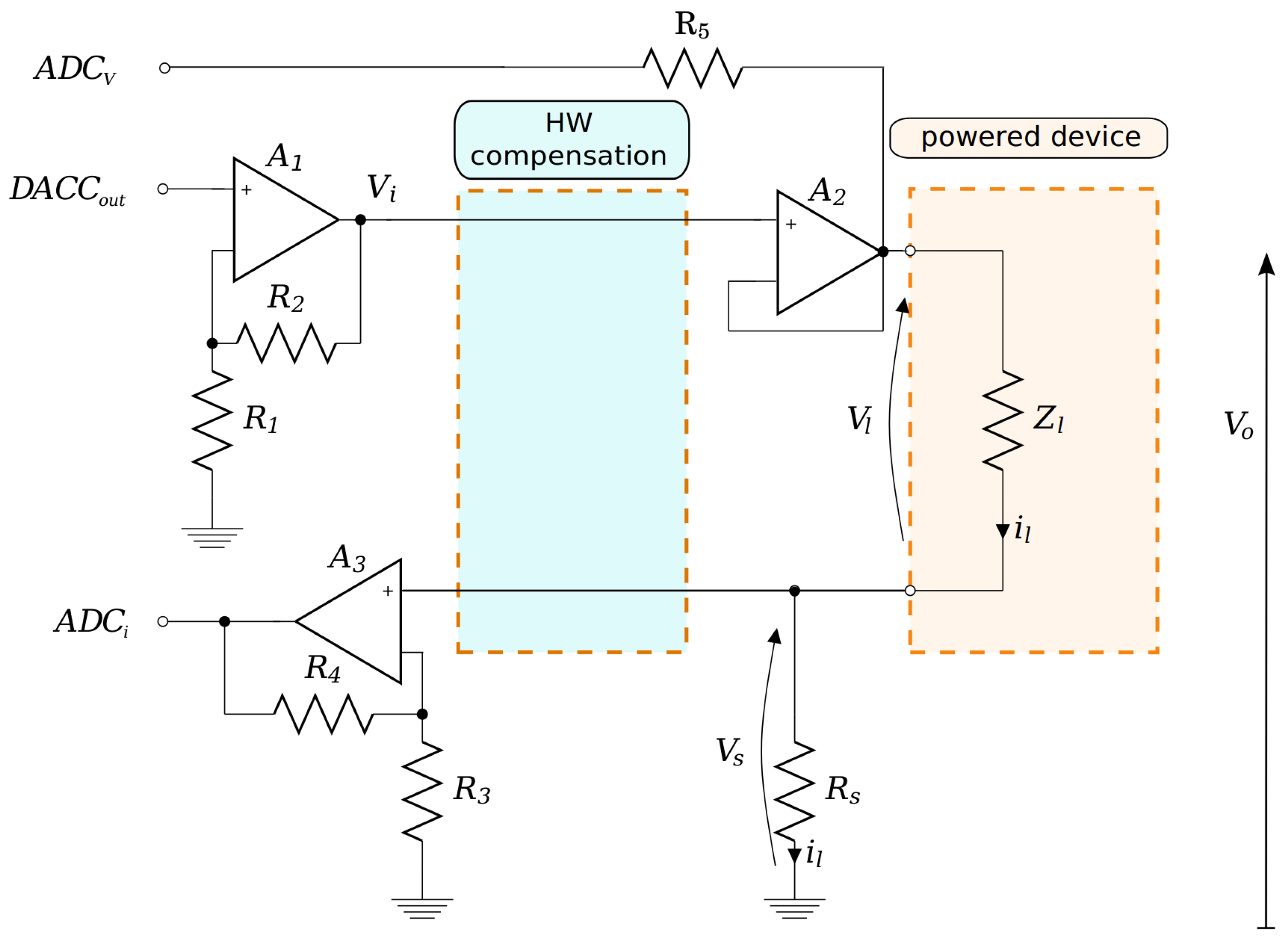
The reference system covered by this study is the energy harvesting embedded emulator presented in [5,6]. The emulator controls the voltage and the current supplied to the powered device by real-time computing a mathematical model representing the emulated energy harvester. The emulator architecture is based on a MCU equipped with analog-to-digital (ADC) and digital-to-analog (DAC) converter channels which allow it to sense and to react as a real energy source. In particular, the main idea on which the system is based, is to continuously measure the current supplied to the load, by means of an ADC, and immediately impose the right voltage output to the load using a DAC. The value of the voltage to be generated is obtained by solving the mathematical model of the emulated source. To better understand the operation of the emulator, we report, in Figure 1, the basic schematic of the interface between the electric load (the device to be powered) and the MCU in charge of controlling the emulation.
The load, which can be a low-power device such as a sensor network mote, is represented in the circuit by a dashed rectangle containing the impedance . The emulator MCU controls the supply voltage by means of the channel coupled to the load through two cascade blocks that make use of the operational amplifiers and .
The first amplifier block which contains , , and , is used to boost the output of the DAC of the MCU into a voltage range suitable for the load device characteristics. The second block is composed of operational amplifier in voltage follower configuration, in order to provide the required decoupling between the DAC output circuit and the load.
The current drawn by the load () is a function of the supply voltage () and of the load impedance , and it is indirectly measured by estimating the voltage drop across the resistor. This resistor is placed between the load and the ground and is used by the MCU as an input of the mathematical model describing the energy harvester, in order to calculate the right value of the voltage to be supplied to the powered device.
An amplifier stage, composed of , , and , amplifies the voltage in order to match the ADC working conditions before carrying it to the channel which performs the digital conversion. A second ADC channel, namely , is used to monitor the value at the output of the voltage buffer for debugging purposes.
The sensing resistor introduces a reduction on the voltage supplied to the load with respect to the nominal value imposed by the emulator (i.e., the amplified DAC signal) according to the EH model. The hardware compensation mechanism, based on an analog circuit, boosts the voltage set by the DAC channel of the MCU by a quantity equal to . This hardware based mechanism dynamically and automatically counterbalances the voltage drop caused by the sensing resistor, with beneficial effects in terms of reactiveness of the emulation. Figure 2 reports the schematic diagram of the emulator encompassing the hardware compensation components (enclosed within a shaded polygon). The compensation stage is built around an operational amplifier () working as voltage follower and an operational amplifier () in summing configuration (with resistors , , , ). The voltage follower decouples the sensing resistor from the adder which sums the voltage value to the voltage output set by the DAC. The sum between the voltage signal from the DAC channel and the voltage signal across the sensing resistor is finally buffered thanks to the voltage follower based on .
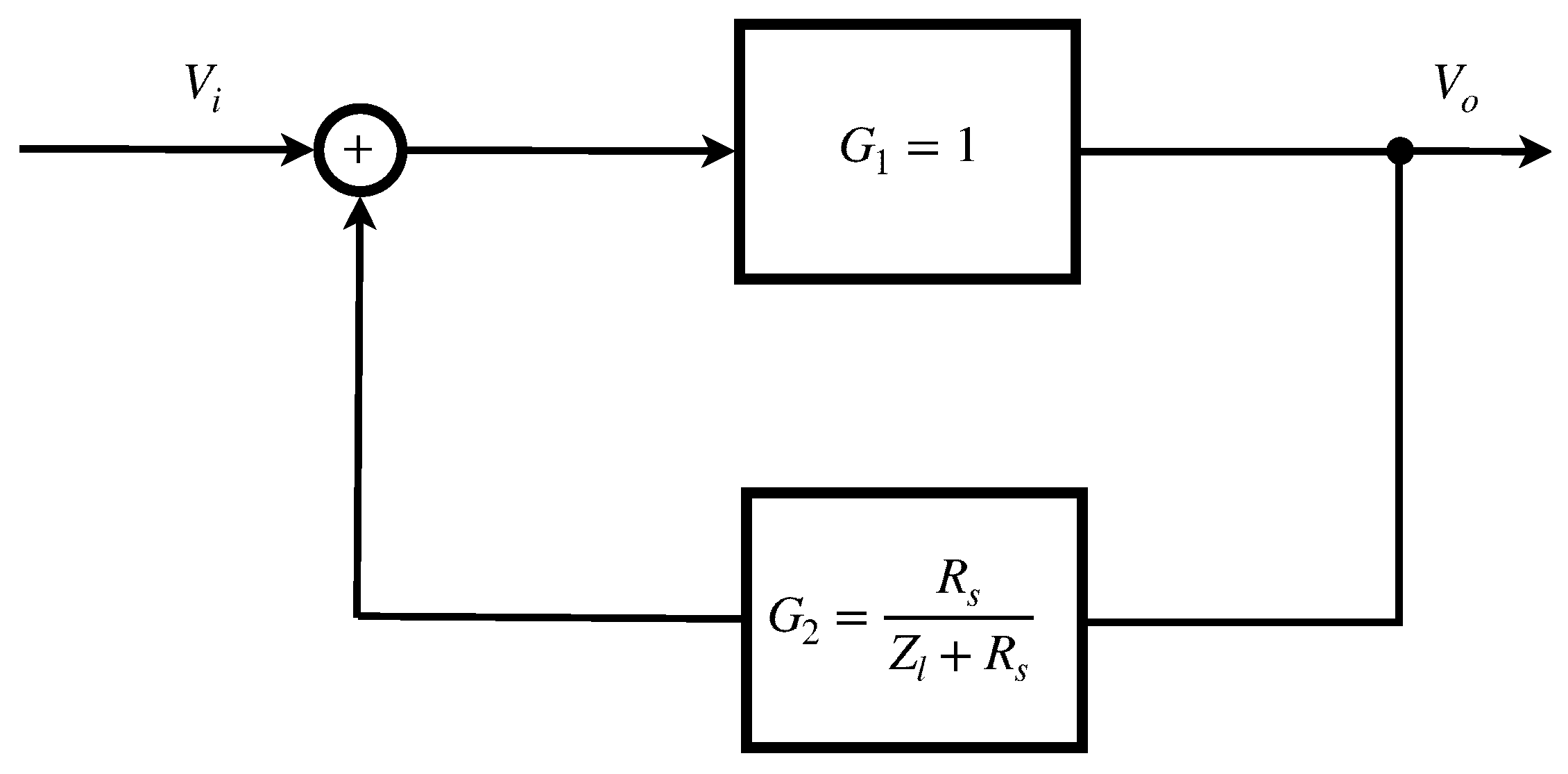
4. Stability Analysis
To derive some results regarding the stability of the embedded emulator under study, we first identify its building blocks, and how they are logically interconnected. Referring to the circuit schematic depicted in Figure 2, the hardware compensation circuit (highlighted by means of the shaded polygon) is based on the following components:
- Input (): the voltage difference (w.r.t. to the common ground reference) provided by the DAC and properly amplified (through , , ).
- A summing junction implemented through the circuit composed of and , , , , .
- A subsystem encompassing: the voltage follower implemented by means of and the load, characterized by an impedance .
- A subsystem implementing the feedback from output to input encompassing: the sensing resistance and the voltage follower implemented by means of .
- : the voltage difference at the sensing resistor .
- Output (): the sum between the voltage difference on the load and the voltage difference on the sensing resistance ().
Since voltage followers provide impedance decoupling with unitary gain, the load and act as a voltage divider block, and a positive feedback is implemented at the summing junction, the relationship between and can be written as:
leading to:
Overall, the above described circuit can be studied as a dynamical system, whose block diagram is depicted in Figure 3. In this system, we can identify two sub-systems ( and ) that are interconnected by means of a positive feedback loop. Their transfer functions can be written, respectively, as and .
From Equation (1), and from the analysis of Figure 3, the transfer function of this system can be written as:
By studying how Equation (2) varies as a function of its independent variables, we can characterize the system and its stability. In particular, we conducted the theoretical analysis for three types of load representatives of realistic operative scenarios, specifically: case study 1 corresponds to a purely resistive load; case study 2 is related to a load composed of a resistance placed in series with a resistance-capacitance (RC) parallel circuit; case 3 considers a load impedance resulting from an inductance placed in series with an RC parallel circuit. Table 1 summarizes the analyzed load types and results (a symbolic notation is used to denote a series (+) or a parallel () connection between electric components).
Case 1:
The transfer function reported in Equation (2) can be written as:
Since it is a constant value (for constant sensing and load resistances), bounded input implies bounded output, and the system is stable [18,19].
Case 2:
Load impedance can be expressed as:
where
Hence:
Poles of this instance of can be derived by imposing , leading to ; since this represents a single pole with real part , we can derive the stability of the system [18,19].
Case 3: Load impedance is given by the following:
Replacing the corresponding term in Equation (2) leads to:
The characteristic equation (i.e., the denominator of H(s)) can be studied to apply Routh criterion. To this aim, the Routh table reported in Table 2 can be built and, from its analysis, we can state the permanence of sign in the second column, from which the demonstration of the stability of the system immediately follows [18].
5. Experimental Set-Up
The emulator has been tested in four different configurations of the connected load, namely: Cases 1, 2, and 3, corresponding to the three configurations analyzed in Section 4 and in a fourth configuration (denoted as Case 4) where the emulator load was a real VirtualSense WSN node [20]. Off-the-shelf discrete components that were used for the experiments take the following values:
- Case 1: .
- Case 2 , .
- Case 3, , , .
During the experiments, the emulator was powered at 12 V by a NGMO2 Rohde & Schwarz dual-channel power supply (Rohde & Schwarz, Munich, Germany) and the digital waveforms were sampled by means of a National Instruments NI-DAQmx PCI-6251 16-channel data acquisition board (National Instruments, Austin, TX, USA) connected to a BNC-2120 shielded connector block (National Instruments, Austin, TX, USA) [21,22,23].
6. Results and Discussion
To experimentally investigate the stability of the compensation mechanism installed on the emulator, we conceived a set of synthetic tests aimed at creating an almost instantaneous perturbation on the working condition in order to evaluate the system dynamic response. A second set of experiments has then been conducted to investigate the system stability under realistic working conditions.
6.1. Synthetic Benchmarks
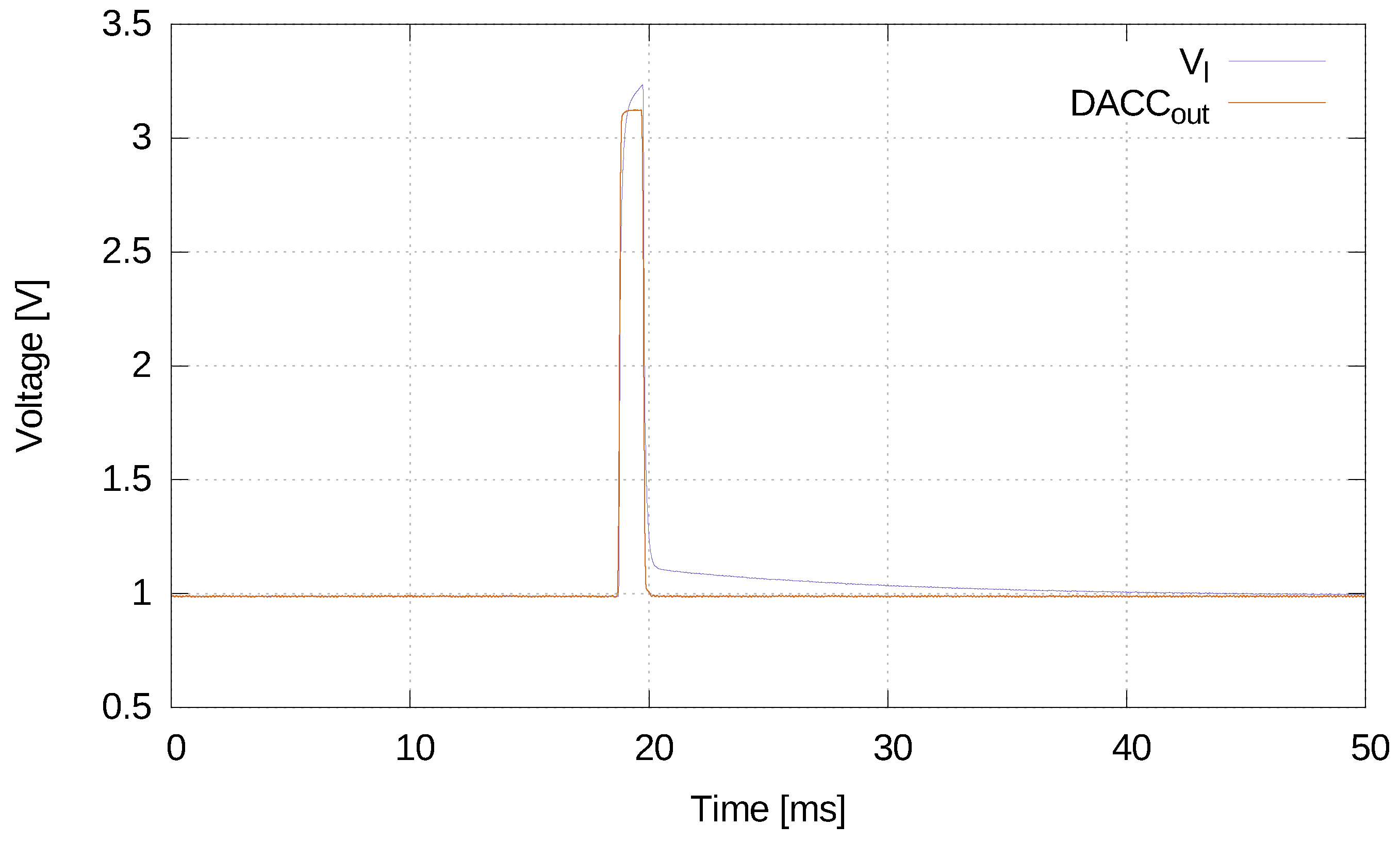
The instantaneous perturbation has been generated by programming the DAC of the emulator to generate a square pulse on the channel. The pulse lasts one millisecond and raises the output voltage from to V and the back to 1 V. In this experiment, the rapid increase of the supply voltage leads to a growth of the current drawn by the load (), which, in turn, decreases the voltage supplied (). The compensation mechanism reacts by boosting the to restore the imposed output (i.e., V) and, when the level goes back to the initial value, the delay of the compensation mechanism causes a measurable over-voltage on the output level that lasts for several milliseconds. This perturbation has been applied to each load configuration described in Section 5 ( 1, 2, 3, and 4) and the waveforms of the and of the signals have been collected and analyzed.
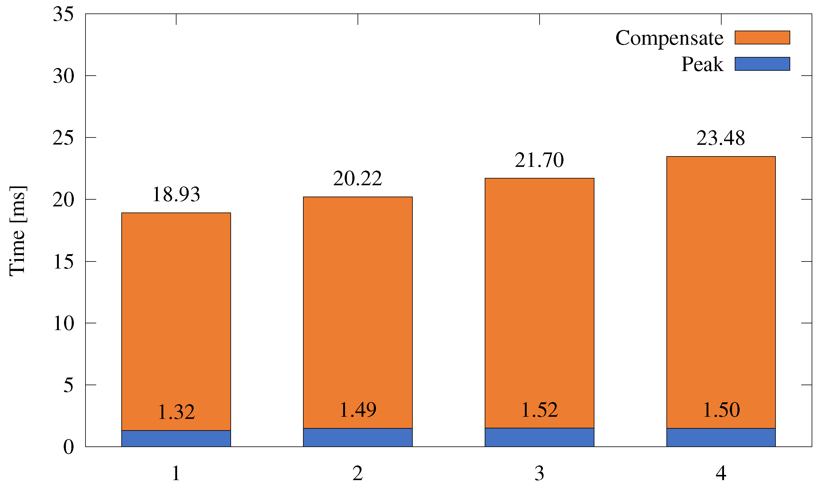
Figure 4 shows the sampled waveforms of the and of the signals during the impulse perturbation when a type-3 load was connected. For the sake of simplicity, relative to the output signal, we call Peak the first part of the disturbance that follows more or less faithfully the input signal, while we call Compensate the part of the residual disturbance which gradually disappears and which is strictly related to the compensation mechanism. The traces have been processed by means of Matlab environment (R2017b, MathWorks, Natick, MA, USA) in order to detect and measure each peak component.
Figure 5 reports the time width of the Peak and of the Compensate part of the disturbance, obtained after a pulse, when the emulator was powering loads in cases 1, 2, 3, and 4. During each experiment, no evidence of unstable behavior has been found, but a slight correlation of the duration of the over-voltage phase with the complexity of the connected load has been highlighted. In particular, in the simple Case 1 load configuration, the average value of the Compensate phase was milliseconds, while, in Case 2 and 3 configurations, it was respectively and milliseconds. The largest value of about milliseconds has been obtained when the emulator was powering a real sensor mote (Case 4 configuration). On the other hand, the width of the Peak phase is only marginally affected by the load variation so that it ranges from about milliseconds in 1 to about milliseconds when powering a real sensor node.
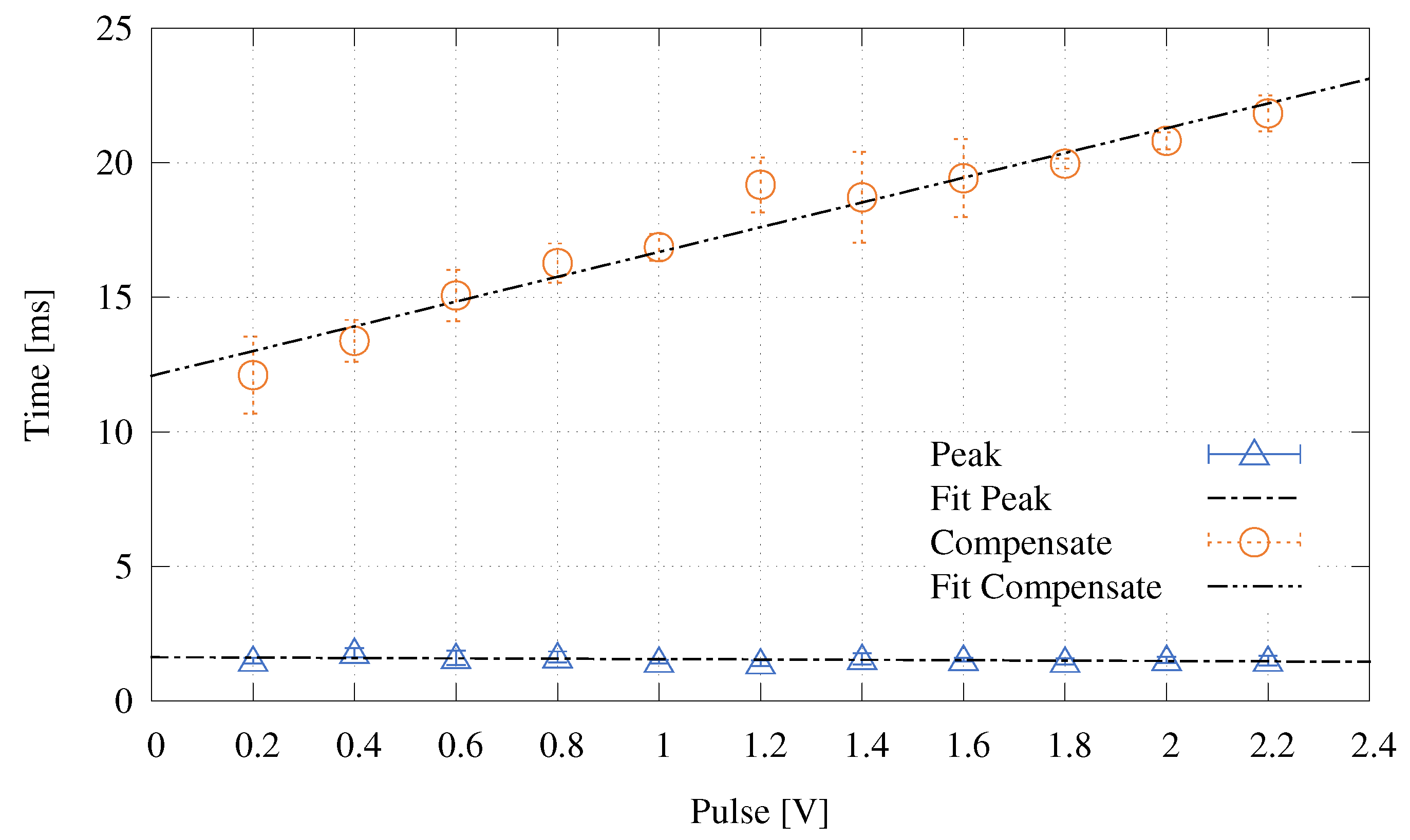
A second set of experiments has been carried out to more deeply investigate the response of the system to a rapid impulse. In particular, the pulse magnitude imposed on the was varied between 0.2 and 2.2 Volts and the induced over-voltage phase has been characterized. Figure 6 shows the width of the Peak and of the Compensate phases measured while the pulse magnitude was increased. Interestingly, the width of the Compensate phase shows a strong linear dependence on the pulse magnitude while the width of the Peak remains almost constant.
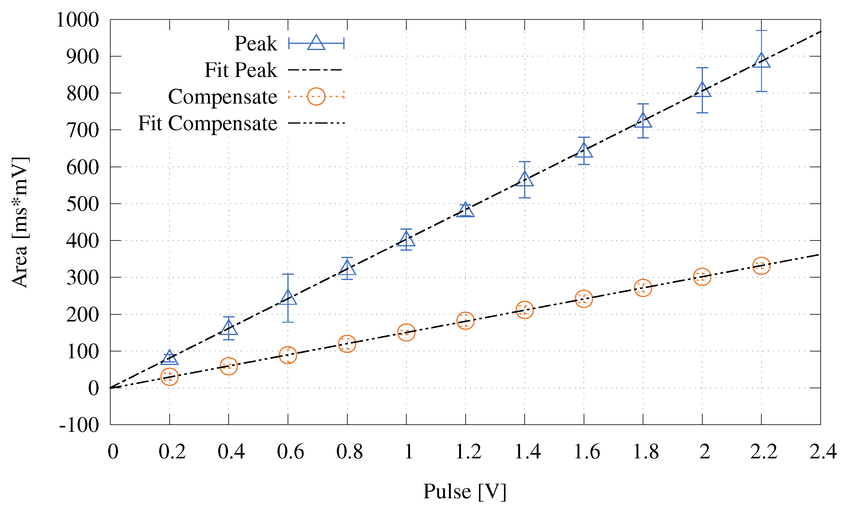
Figure 7 reports the area of the Peak and Compensate phases when increasing the pulse magnitude. In this case, the dependence on the magnitude of the pulse is strictly linear for both phases even if they show a different slope. In addition, in this set of experiments, the system was always stable, confirming the theory described in Section 4.
6.2. Typical Sensor Node Task
Once the stability of the system to an artificial impulse has been proved, we carried out several experiments in realistic scenarios. In particular, a frequent working condition for an energy harvester emulator is to power a sensor node equipped with a low-power microcontroller. Modern System on a Chip (SoC) microcontrollers normally alternate their operating conditions between several states, with different power consumption, depending on the activity they are carrying out (i.e., sensing quantities, processing data, sending packet wirelessly, etc.). These state transitions are almost instantaneous and cause a rapid change on the applied load, with a consequent rapid change in the current supplied by the emulator (). This entails a rapid need to compensate for the voltage applied to the sensor node () which, potentially, can cause unstable dynamics.
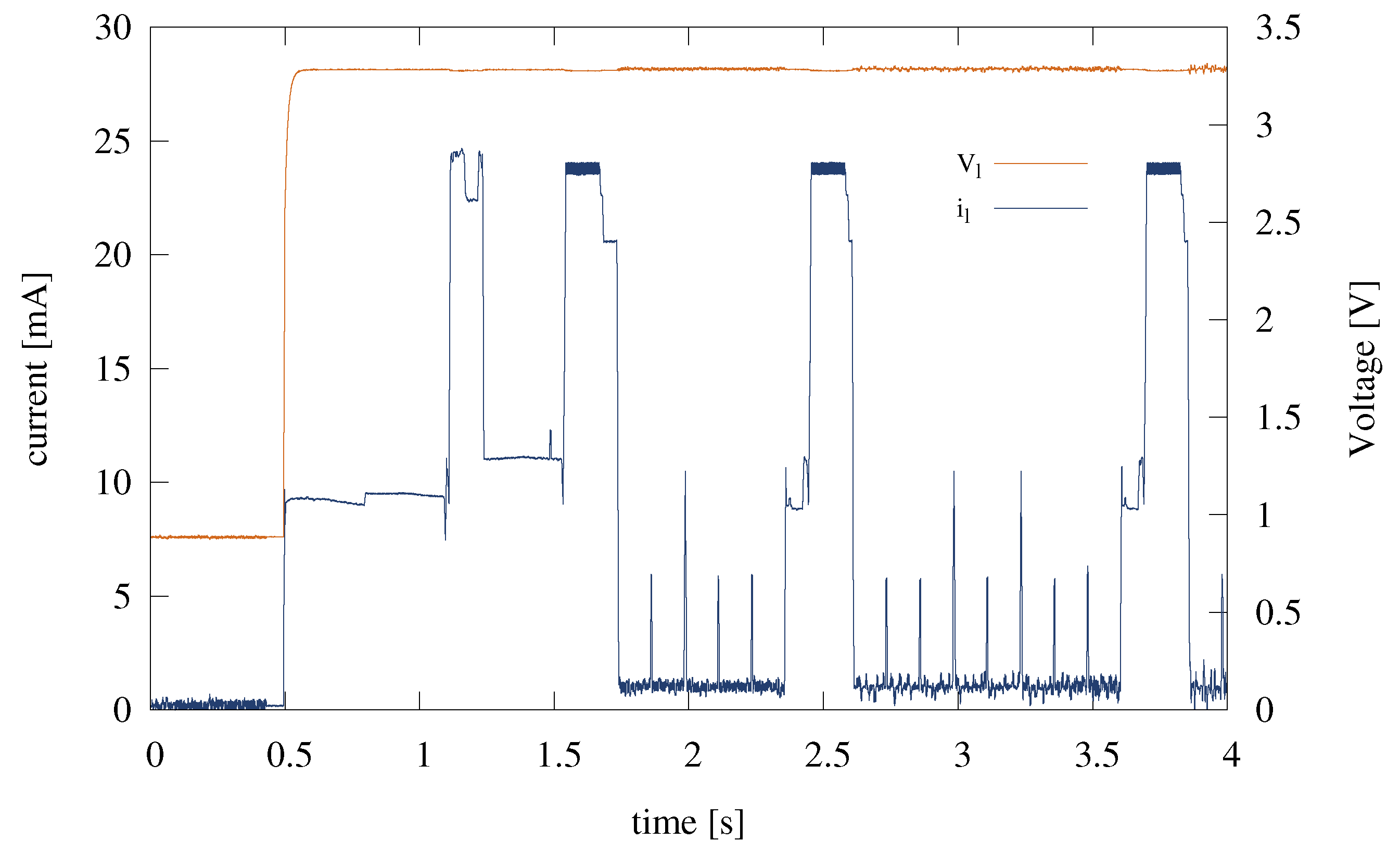
Figure 8 shows the waveform (red line) sampled at 100 kHz while powering a VirtualSense node together with the trace (blue line) representing the current drawn by the sensor. At 0.5 s, the emulator starts powering the sensor by setting the to its working conditions (i.e., 3.3 Volts). Consequently, the node boots the operating system (from 0.5 to 1.5 s) and then starts its main task. In this experiment, the only task installed on the node was periodically sending a broadcast packet containing 100 bytes by means of the ContikiMAC radio duty cycling protocol. In the current trace, a high power consumption phase (about 24 mA) corresponds to each transmission, lasting about 300 milliseconds, followed by a low power phase (about 1 mA), which lasts until the next packet is sent. The low power phase is, in turn, periodically interrupted by a rapid spike in the power consumption due to the Channel Clear Assessment (CCA) performed by the ContikiMAC protocol to probe the channel occupancy.
As proof of the stability of the compensation system, it is possible to note that, although state transitions are almost immediate, the value of imposed by the emulator is perfectly constant, and it does not show any unstable dynamics.
7. Conclusions
Emulation of energy harvesting sources represents an interesting solution in the design and test of networked embedded systems. In particular, when applied to gain knowledge on the behavior of systems composed of low power devices, it potentially enables experimental validations in a reproducible and realistic way.
In this article, we presented a study aimed at evaluating a hardware-software solution recently proposed in scientific literature. The analyzed system is built around an embedded ultra-low power platform targeting low-cost and small form factor. Moreover, it has been demonstrated as being capable of guaranteeing good levels of accuracy when reproducing the response of an energy harvester, with latencies compatible with real-time requirements. Since the reduced delay performance is obtained thanks to a hardware compensation mechanism implementing a positive feedback loop, it is interesting to investigate its stability, which is the focus of this work. In particular, we analyzed how the system stability depends on the type of powered load by proving theoretical stability results under several scenarios, and we also experimentally tested the dynamics of the platform in realistic frameworks.
Overall, the presented results demonstrate the theoretical stability of the system in a wide range of possible set-ups, and provide evidence of the capability of the emulator to react to sudden changes of its operating conditions (for instance because of modification of the load impedance) without driving its dynamics towards unstable regimes.
Author Contributions
Conceptualization, V.F. and E.L.; methodology, V.F. and E.L.; theoretical stability analysis, V.F.; experimental set-up design and experiments, E.L.; writing, review, and editing, V.F. and E.L.
Funding
This research received no external funding.
Conflicts of Interest
The authors declare no conflict of interest.
References
- Adu-Manu, K.S.; Adam, N.; Tapparello, C.; Ayatollahi, H.; Heinzelman, W. Energy-harvesting wireless sensor networks (EH-WSNs): A review. ACM Trans. Sens. Netw. (TOSN) 2018, 14, 10. [Google Scholar] [CrossRef]
- Gunduz, D.; Stamatiou, K.; Michelusi, N.; Zorzi, M. Designing intelligent energy harvesting communication systems. IEEE Commun. Mag. 2014, 52, 210–216. [Google Scholar] [CrossRef]
- Jung, H.J.; Song, Y.; Hong, S.K.; Yang, C.H.; Hwang, S.J.; Jeong, S.Y.; Sung, T.H. Design and optimization of piezoelectric impact-based micro wind energy harvester for wireless sensor network. Sens. Actuators A Phys. 2015, 222, 314–321. [Google Scholar] [CrossRef]
- Bogliolo, A.; Lattanzi, E.; Freschi, V. Idleness as a Resource in Energy-Neutral WSNs. In Proceedings of the 1st International Workshop on Energy Neutral Sensing Systems, Rome, Italy, 13 November 2013; ACM: New York, NY, USA, 2013; pp. 1–6. [Google Scholar]
- Lattanzi, E.; Freschi, V. A Hardware Compensation Mechanism for Embedded Energy Harvesting Emulation. IEEE Embed. Syst. Lett. 2019, 11, 25–28. [Google Scholar] [CrossRef]
- Lattanzi, E.; Freschi, V.; Dromedari, M.; Lorello, L.S.; Peruzzini, R.; Bogliolo, A. A fast and accurate energy source emulator for wireless sensor networks. EURASIP J. Embed. Syst. 2017, 2016, 18. [Google Scholar] [CrossRef]
- Bobovych, S.; Banerjee, N.; Robucci, R.; Parkerson, J.P.; Schmandt, J.; Patel, C. SunaPlayer: high-accuracy emulation of solar cells. In Proceedings of the 14th International Conference on Information Processing in Sensor Networks (IPSN ’15), Seattle, WA, USA, 14–16 April 2015; pp. 59–70. [Google Scholar]
- Hester, J.; Scott, T.; Sorber, J. Ekho: Realistic and Repeatable Experimentation for Tiny Energy-Harvesting Sensors. In Proceedings of the 12th ACM Conference on Embedded Network Sensor Systems (SenSys ’14), Memphis, TN, USA, 3–6 November 2014; pp. 1–15. [Google Scholar]
- Chou, P.H.; Park, C.; Park, J.; Pham, K.; Liu, J. B#: A battery emulator and power profiling instrument. IEEE Des. Test Comput. 2005, 22, 150–159. [Google Scholar]
- Albertus, P.; Newman, J. Introduction to Dualfoil 5.0; Tech. Rep; University of California Berkeley: Berkeley, CA, USA, 2007. [Google Scholar]
- Li, D.J.; Chou, P.H. Maximizing efficiency of solar-powered systems by load matching. In Proceedings of the 2004 International Symposium on Low Power Electronics and Design, Newport Beach, CA, USA, 9–11 August 2004; pp. 162–167. [Google Scholar]
- Lee, W.; Kim, Y.; Wang, Y.; Chang, N.; Pedram, M.; Han, S. Versatile high-fidelity photovoltaic module emulation system. In Proceedings of the International Symposium on Low Power Electronics and Design, Fukuoka, Japan, 1–3 August 2011; pp. 91–96. [Google Scholar]
- Thale, S.; Wandhare, R.; Agarwal, V. A novel low cost portable integrated solar PV, fuel cell and battery emulator with fast tracking algorithm. In Proceedings of the 40th Photovoltaic Specialist Conference (PVSC), Denver, CO, USA, 8–13 June 2014; pp. 3138–3143. [Google Scholar]
- Chen, C.C.; Chang, H.C.; Kuo, C.C.; Lin, C.C. Programmable energy source emulator for photovoltaic panels considering partial shadow effect. Energy 2013, 54, 174–183. [Google Scholar] [CrossRef]
- González-Medina, R.; Patrao, I.; Garcerá, G.; Figueres, E. A low-cost photovoltaic emulator for static and dynamic evaluation of photovoltaic power converters and facilities. Prog. Photovolt. Res. Appl. 2014, 22, 227–241. [Google Scholar] [CrossRef]
- Zhang, H.; Salajegheh, M.; Fu, K.; Sorber, J. Ekho: Bridging the Gap Between Simulation and Reality in Tiny Energy-Harvesting Sensors. In Proceedings of the 4th Workshop on Power-Aware Computing and Systems (HotPower ’11), Cascais, Portugal, 23 October 2011; pp. 1–5. [Google Scholar]
- Hester, J.; Sitanayah, L.; Scott, T.; Sorber, J. Realistic and Repeatable Emulation of Energy Harvesting Environments. ACM Trans. Sen. Netw. 2017, 13, 16. [Google Scholar] [CrossRef]
- Dorf, R.C.; Bishop, R.H. Modern Control Systems; Pearson: London, UK, 2011. [Google Scholar]
- Aström, K.J.; Murray, R.M. Feedback Systems: An Introduction for Scientists and Engineers; Princeton University Press: Princeton, NJ, USA, 4 March 2010. [Google Scholar]
- Raza, U.; Bogliolo, A.; Freschi, V.; Lattanzi, E.; Murphy, A.L. A two-prong approach to energy-efficient WSNs: Wake-up receivers plus dedicated, model-based sensing. Ad Hoc Netw. 2016, 45, 1–12. [Google Scholar] [CrossRef] [Green Version]
- NGMO2 Datasheet. Available online: http://www.rohde-schwarz.it/file_1800/ngmo2_21_web-LF.pdf (accessed on 15 January 2018).
- PC-6251 Datasheet. Available online: http://sine.ni.com/nips/cds/print/p/lang/en/nid/14124 (accessed on 15 January 2018).
- BNC-2120 Datasheet. Available online: http://sine.ni.com/nips/cds/view/p/lang/en/nid/10712 (accessed on 15 January 2018).
Figure 1.
The current emulation interface with the hardware compensation module.

Figure 2.
Schematic diagram of the current emulation interface with the hardware compensation circuit highlighted.
Figure 2.
Schematic diagram of the current emulation interface with the hardware compensation circuit highlighted.

Figure 3.
Schematic diagram of the feedback loop implemented by means of the hardware compensation circuit.
Figure 3.
Schematic diagram of the feedback loop implemented by means of the hardware compensation circuit.

Figure 4.
and pulse traces.

Figure 5.
pulse width for different emulator load types.

Figure 6.
Peak and Compensate width versus pulse magnitude.

Figure 7.
Peak and Compensate area versus pulse magnitude.

Figure 8.
and traces collected while the emulator was powering a wireless sensor node that was transmitting 100 bytes broadcast packets.
Figure 8.
and traces collected while the emulator was powering a wireless sensor node that was transmitting 100 bytes broadcast packets.


Table 1.
Theoretical stability analysis: case studies.
| Case nr. | Load Type | Stable |
|---|---|---|
| 1 | R | ✓ |
| 2 | ✓ | |
| 3 | ✓ |
Table 2.
Routh table.
| 2 | RLC | R |
| 1 | L | 0 |
| 0 | R | 0 |
© 2019 by the authors. Licensee MDPI, Basel, Switzerland. This article is an open access article distributed under the terms and conditions of the Creative Commons Attribution (CC BY) license (http://creativecommons.org/licenses/by/4.0/).
Share and Cite
MDPI and ACS Style
Freschi, V.; Lattanzi, E. On the Stability of a Hardware Compensation Mechanism for Embedded Energy Harvesting Emulators. Computers 2019, 8, 78. https://0-doi-org.brum.beds.ac.uk/10.3390/computers8040078
AMA Style
Freschi V, Lattanzi E. On the Stability of a Hardware Compensation Mechanism for Embedded Energy Harvesting Emulators. Computers. 2019; 8(4):78. https://0-doi-org.brum.beds.ac.uk/10.3390/computers8040078
Chicago/Turabian StyleFreschi, Valerio, and Emanuele Lattanzi. 2019. "On the Stability of a Hardware Compensation Mechanism for Embedded Energy Harvesting Emulators" Computers 8, no. 4: 78. https://0-doi-org.brum.beds.ac.uk/10.3390/computers8040078
Note that from the first issue of 2016, this journal uses article numbers instead of page numbers. See further details here.