Effects of GaN Buffer Resistance on the Device Performances of AlGaN/GaN HEMTs

1
Advanced Material Research Center, Kumoh National Institute of Technology, Gumi 39177, Korea
2
Yield Enhancement Team, Foundry, Samsung Electronics Company Ltd., Yongin 17113, Korea
3
Department of Advanced Materials Science and Engineering, Kumoh National Institute of Technology, Gumi 39177, Korea
*
Author to whom correspondence should be addressed.
Crystals 2020, 10(9), 848; https://doi.org/10.3390/cryst10090848
Submission received: 20 August 2020
/
Revised: 15 September 2020
/
Accepted: 22 September 2020
/
Published: 22 September 2020
(This article belongs to the Special Issue Nano/Micro and Bio-Inspired Materials on Wide-Bandgap-Semiconductor-Based Optoelectronic/Power Devices)
Abstract
:We investigated the effects of GaN buffer resistance of AlGaN/GaN high-electron-mobility transistors (HEMTs) on direct current (DC), low-frequency noise (LFN), and pulsed I-V characterization performances. The devices with the highest GaN buffer resistance were grown on sapphire substrate using two-step growth temperature method without additional compensation doping. The proposed device exhibited the degraded off-state leakage current due to the improved GaN buffer quality compared to the reference devices with relative low buffer resistance, which is confirmed by high resolution X-ray diffraction (HRXRD). However, the proposed device with deep-level defects in GaN buffer layer showed the reduced hysteresis (∆Vth), increased breakdown voltage (BV), and enhanced pulse I-V characteristics. Regardless of GaN buffer resistance, all devices clearly showed 1/f behavior with carrier number fluctuations (CNF) at on-state but followed 1/f2 characteristic at off-state. From the 1/f2 noise characteristics, the extracted trap time constant (τi) of the proposed device can be obtained to be 10 ms, which is shorter than those of the reference devices because of the full compensation of deep-level defects in the GaN buffer layer.

1. Introduction
AlGaN/GaN high-electron-mobility transistors (HEMTs) have many advantages for power device applications because of their excellent material properties such as high band-gap and large breakdown electric field. For adopting the AlGaN/GaN HEMT to a power device, the high-resistivity (HR) or semi-insulating (SI) GaN buffer layer is required to not only minimize the off-state leakage current, but also mitigate current collapse. Many technologies for developing the HR GaN buffer layer have been reported by utilizing (1) the generation of the deep-level defects or dislocations through controlling the growth temperature [1,2] and (2) the doping of deep-level impurities such as Fe, Mg, or C atoms [3,4,5]. These deep-level defects and impurities mostly compensate the background n-type residual donors in conventional unintentional doped GaN buffer layer due to the nitrogen vacancies (VN) and/or oxygen (O) atoms. The additional compensation doping method severely suffers from the memory effect, redistribution of dopant atoms, and unexpected trapping effects [3,4,5]. On the other hand, it is easy and simple method to intentionally introduce the deep-level defects by controlling the growth temperature for achieving the HR GaN buffer layer. Lee et al. [1] reported to the device performances of normally off GaN MOSFETs with extremely high resistive buffer layer by utilizing the two-step growth temperature. However, no detailed comprehensive analyses regarding the AlGaN/GaN HEMTs with the different GaN buffer resistance have been performed in view of low frequency noise (LFN) measurements. LFN can have great advantages to investigate the interface and/or oxide traps as well as buffer traps when operated at both on-state and off-state. The effect of the passivation of AlGaN/GaN HEMTs on LFN was reported by Veriatchikh et al. [6]. Our groups investigated LFNs of AlGaN/GaN HEMTs with C-doped GaN buffer layer [7]. In this work, we fabricate and characterize AlGaN/GaN HEMTs with different GaN buffer resistance by considering direct current (DC), LFN, and pulsed I–V measurements. These characterizations give information on the origin of traps in the fabricated devices and the effects of the traps in the GaN buffer layer on the device performances.
2. Materials and Methods
The AlGaN/GaN heterostructures with different GaN buffer resistance were grown on a 4-in c-plain sapphire substrate by metal organic chemical vapor deposition, which consists of 30-nm-thick low-temperature-grown initial GaN layer, 3-μm-thick highly resistive undoped GaN buffer layer, and 25-nm-thick AlGaN barrier. In order to get high GaN buffer resistance, the initial low growth temperature was set to be 950 °C and then increased to 1050 °C, which is named by two-step growth. As decreased the initial growth temperature, the grain sizes are decreased and nuclei densities are increased [1]. When the growth temperature of GaN layer was 950 °C for 2 min (~100 nm thickness), the subsequently grown GaN layer was generated too many deep-level defects, which plays a role with high resistive properties in the GaN buffer layer [1,2]. For comparison, two samples were prepared using one-step growth method grown at 1000 °C and 1020 °C, respectively. The growth temperature of AlGaN barrier layer for all samples was fixed to 1100 °C. Hall effect measurements at room temperature for GaN buffer layer without AlGaN layer showed the sheet resistances (Rsh) of over 109 Ω/sq (unmeasurable value) for two-step growth. The Rsh for the reference samples using one-step growth was greatly reduced from 106 Ω/sq to 104 Ω/sq with increasing growth temperature from 1000 °C to 1020 °C. The detailed structure and electrical properties for the grown AlGaN/GaN heterostructure with different buffer resistances were summarized in Table 1.
For the device isolation, mesa etching was performed to a etch depth of 500 nm using inductively coupled plasma-reactive ion etching (ICP-RIE) using a Cl2 gas. After cleaning the wafer, a Si/Ti/Al/Ni/Au stack for ohmic contacts was deposited by electron-beam evaporator and then followed by rapid thermal annealing at 850 °C for 30 s. Finally, Ni/Au gate metal was deposited to form the gate length (Lg) of 5 µm (gate-drain spacing (Lgd) of 4 μm). The device structure is illustrated in Figure 1.
3. Results and Discussion
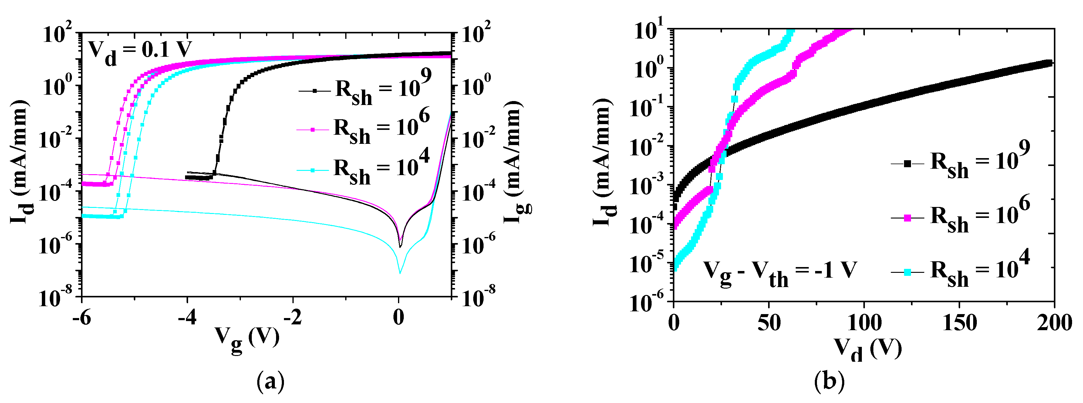
The drain currents for the fabricated AlGaN/GaN HEMTs with different GaN buffer resistance were measured with applying double gate voltage sweep (negative to positive sweep and then positive to negative sweep) in Figure 2a. The proposed device using two-step growth exhibits the positive shift of threshold voltage (Vth) with approximately −3 V compared to the reference devices. The reason for the positive Vth is due to the relatively small carrier concentration (ns) compared to large ns of the reference devices induced by the combination of two-dimensional electron gas (2DEG) channel and the GaN channel (Hall results in Table 1). It is also interesting to note that the proposed device presents negligible hysteresis of 20 mV, while the devices with Rsh = 106 and 104 indicate to large hysteresis of 180 mV and 220 mV, respectively. This means that the proposed device has less trapping effect into the deep-levels in GaN buffer layer, as discussed later. On the other hand, the off-state leakage current in the proposed device is the highest value that those of the reference devices, as shown in Figure 2. It is attributed to the improved crystal quality of GaN buffer layer for the proposed sample, which is confirmed by high-resolution X-ray diffraction (HRXRD) and atomic force microscopy (AFM) (Table 1). Another possible explanation is the fully compensated GaN buffer layer of the proposed device, which hardly captures some electrons from the off-state leakage and hence do not reduce the leakage current. However, the breakdown voltages (BV) with the devices with Rsh = 109, 106, and 104 demonstrate 185 V, 64 V, and 39 V at Id = 1 mA/mm, respectively, as shown in Figure 2b. The highest BV characteristic for the proposed device is due to the extremely high GaN buffer resistance property.
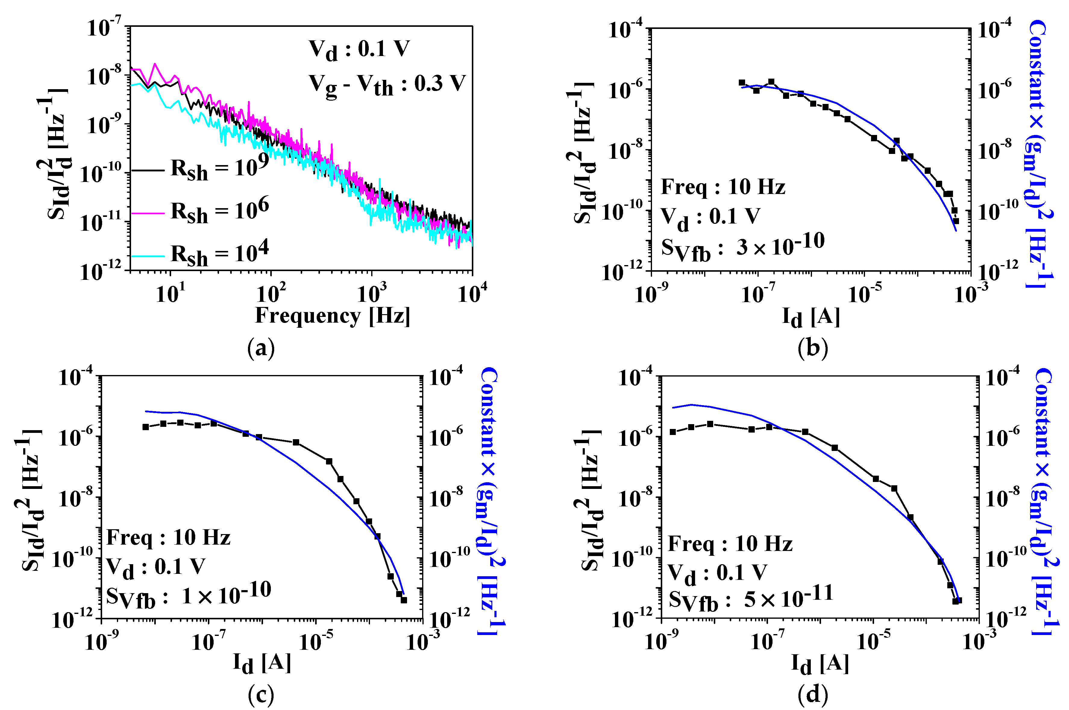
To find the conduction mechanism, the LFN characterizations are conducted using a fully automatic noise measurement system from Synergie Concept (Meylan, France). Noise measurements were performed sweeping the gate voltage (Vg) from subthreshold to strong accumulation region in the linear region (Vd = 0.1 V) and the frequency (f) ranges from 4 Hz to 104 Hz. Regardless of the GaN buffer resistances, all devices exhibit almost identical 1/fγ shape with γ ≈ 1 in entire f range (Figure 3a). Figure 3 shows the normalized noise power spectral densities (SId/Id2) according to the drain currents at f = 10 Hz. Applying to the carrier number fluctuations (CNF) model, we can obtain the origin of trapping-related fluctuations and the trap density using Equation (1) [8,9],
where SVfb is the flatband voltage fluctuations (=q2kTλNt/WLCox2f), including q is the electron charge, kT is the thermal energy, λ is the oxide tunneling attenuation distance, Nt is the volumetric oxide trap density, WL is the channel area, Cox is the gate dielectric capacitance per unit area, and f is frequency. When we match SId/Id2 and (gm/Id)2, the SVfb are calculated to be 3.0 × 10⁻¹⁰ V2·Hz−1 (Figure 3b), 1.0 × 10⁻¹⁰ V2·Hz−1 (Figure 3c), and 5.0 × 10⁻¹¹ V2·Hz−1 (Figure 3d) for the devices with Rsh = 109, 106, and 104, respectively. Considering the equivalent Cox is the value of CAlGaN = 3.2 × 10⁻⁷ F/cm2, the corresponding trap density (Nt) calculated using Equation (1) with λ = 0.11 nm [10] is 1.0 × 1020 cm−3·eV−1, 3.4 × 1019 cm−3·eV−1, and 1.7 × 1019 cm−3·eV−1, respectively. It is remarkable that the Nt value of the proposed device is highest compared to those of the reference devices. This is because the incremental electron trapping/detrapping process from the 2DEG into the improved crystal quality of AlGaN barrier and GaN channel layer when the channel is on-state, as discussed earlier.
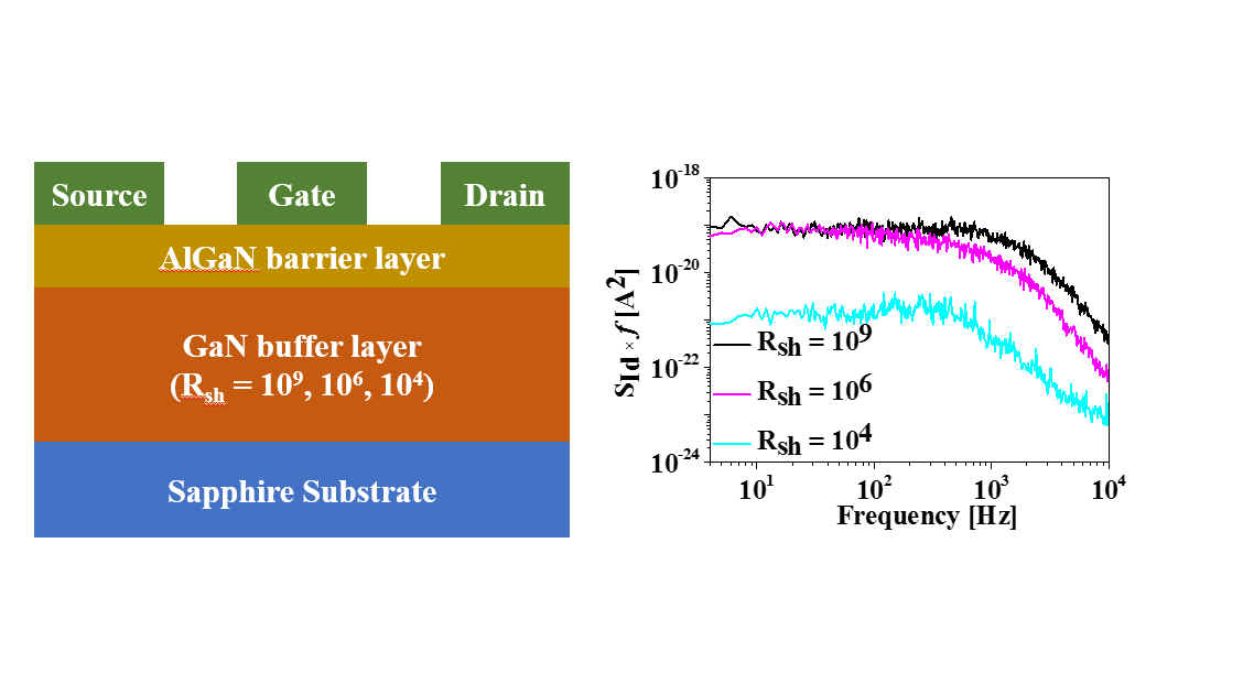
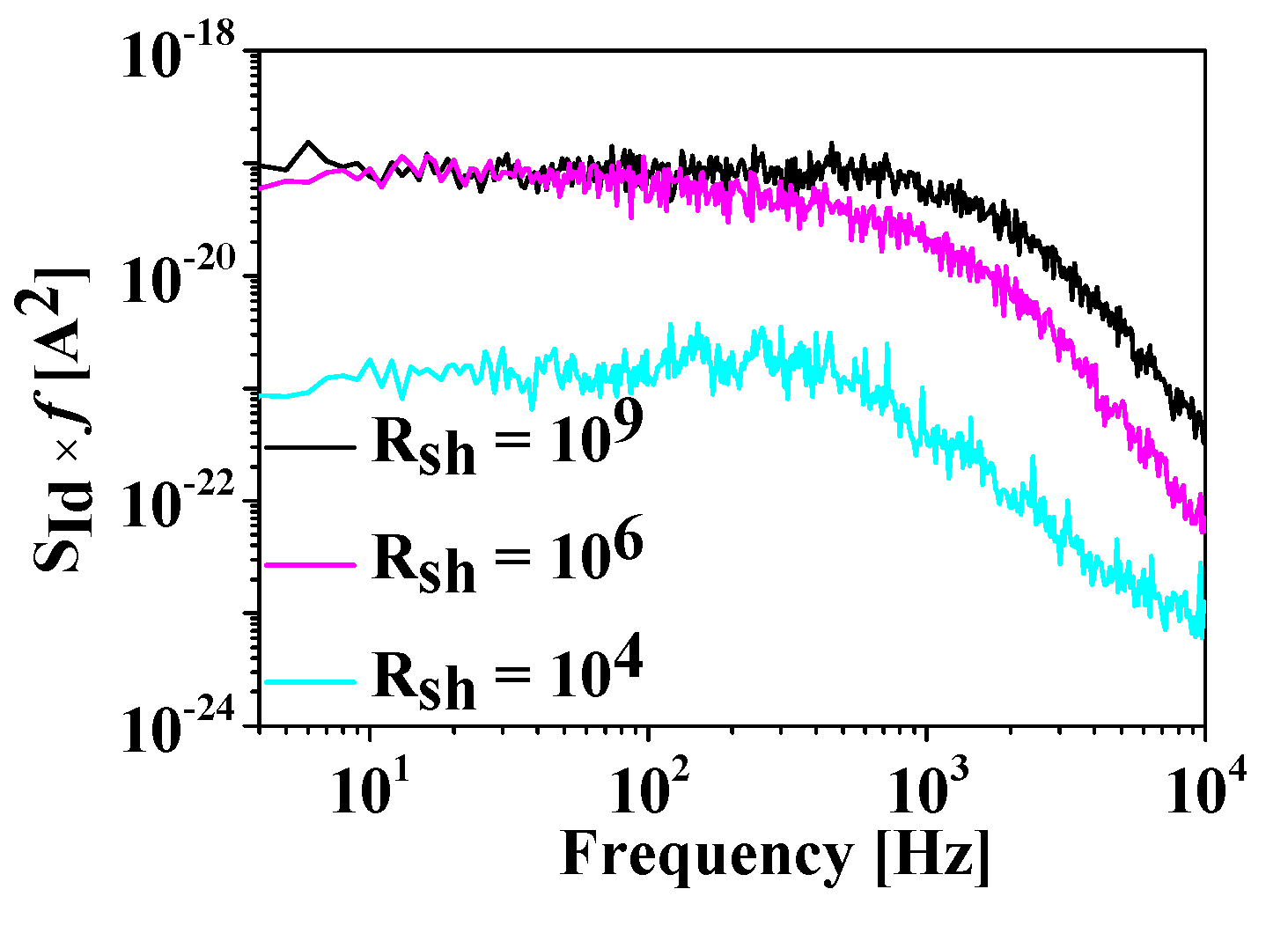
To investigate the noise characteristics according to the buffer resistance, the noise at off-state is measured. Figure 4 shows the product of SId × f for all devices at (Vg – Vth) = −1 V and Vd = 0.1 V to find the generation-recombination (g-r) noise presence on top of 1/f noise. The noise spectra for the proposed device are observed to plateau at low frequency but become suddenly to fall down with 1/f2 at higher frequency, which reflect the co-existence in the spectra of g-r noise with 1/f noise in Equation (2). The reason for the 1/f noise at off-state is because all devices suffer from significant electron trapping/de-trapping into the GaN buffer layer despite at off-state. It is also clearly observed due to the spectral deformations for all devices, which indicated that the g-r process of the deep-level traps in the GaN buffer layer is existed. From the cutoff frequency fo in Figure 4, the trap time constant (τi) can be calculated using the following Equation (2) [11].
where Kf is the coefficient of 1/f noise component, Ai is the plateau value of g-r component, and foi is the cutoff frequency. The τi is extracted to be 1.0 × 10⁻⁴ s, 1.5 × 10⁻⁴, and 3.9 × 10⁻⁴ s for the device with Rsh = 109, 106, and 104, respectively, using fo = 1.5, 1.0, and 0.4 kHz. The proposed device presents the shortest trap time constant, which indicates that the device suffers from less trapping effects through the fully compensated deep-level traps in the GaN buffer layer, as described later.
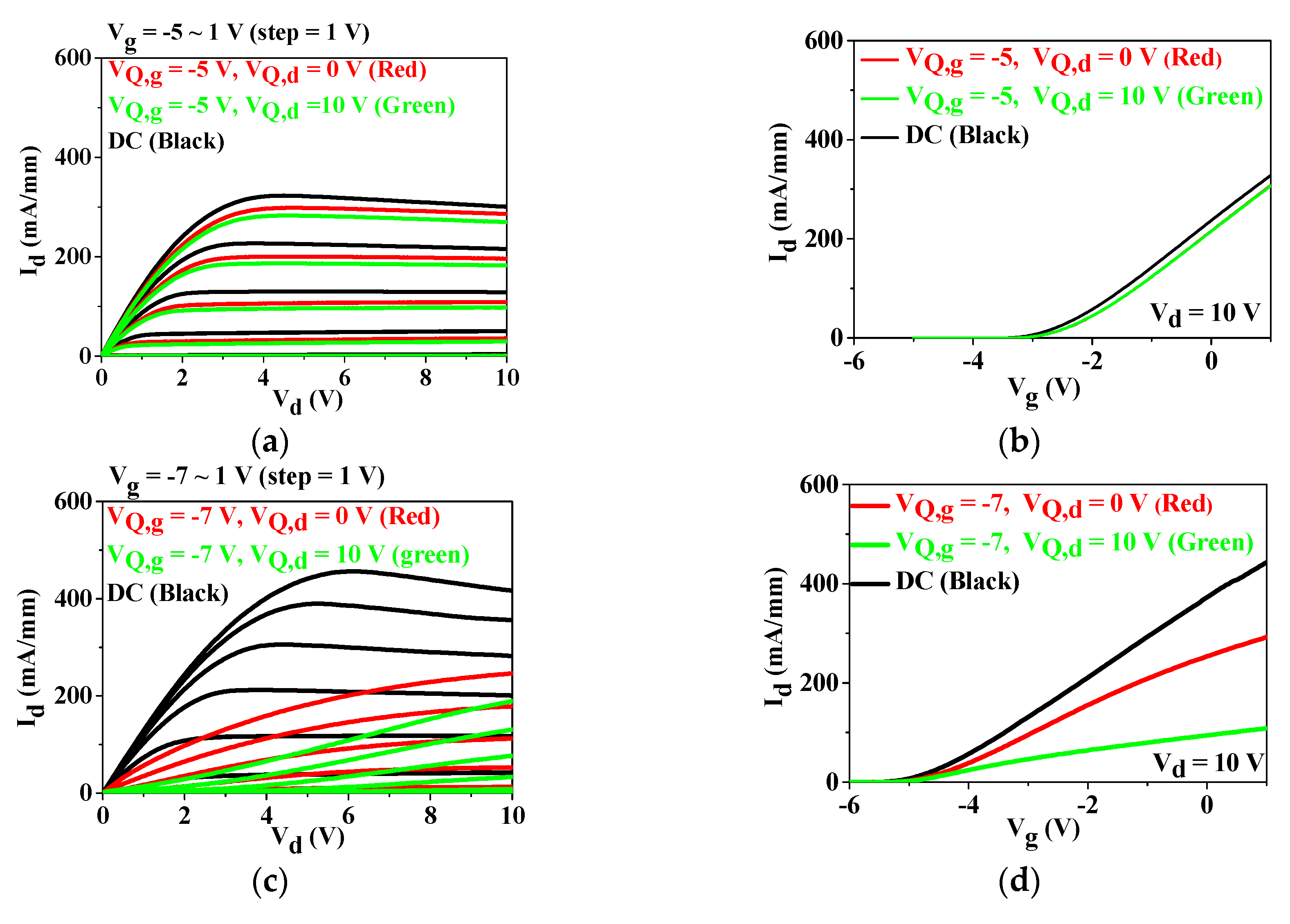
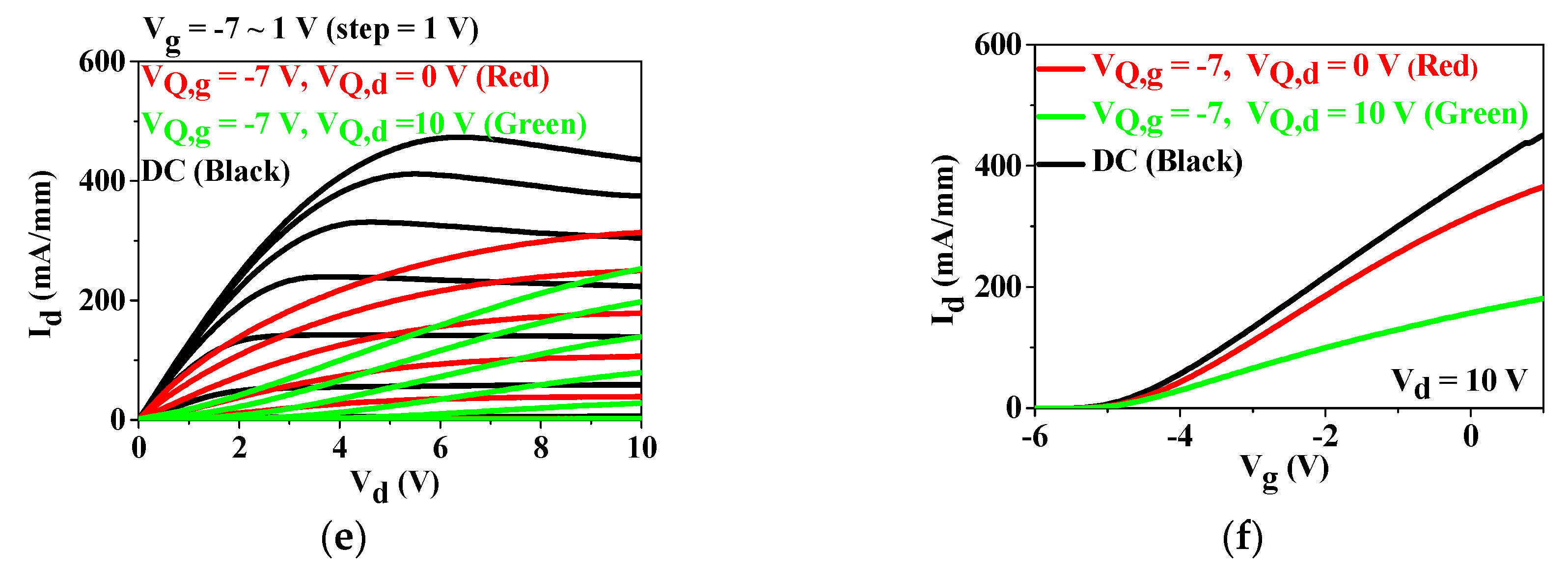
To further identify the trapping effect observed from the DC and noise results, the pulse I-V curves for all devices are measured using B1500 machine from Keysight (Figure 5). The pulse width and pulse length are 1 ms and 1 ms, respectively, and the drain voltage is varied from 0 V to 10 V at Vth < Vg < 1 V. The quasi-bias pulse conditions are set to (i) VQ,g < Vth and VQ,d = 0 V (red lines) to check the gat lag and (ii) VQ,g < Vth and VQ,d = 10 V (green lines) to find the drain lag. The static or dc Id-Vd curves (black lines) are compared to those of the pulse Id-Vd curves as a reference. As shown in Figure 5a,b, the proposed device exhibits the small current collapse for all pulse conditions due to the fully compensated GaN buffer layer. On the other hand, the reference devices present severe current collapses because of uncompensated or unoccupied neutral deep traps in the GaN buffer layer, which can easily capture some electrons from the 2DEG channel when applying high drain voltage (Figure 5c–f) [5]. These pulsed I–V results of the AlGaN/GaN HEMTs are consistent with hysteresis, BV, and noise performances at off-state observed from the devices with different GaN buffer resistance.
4. Conclusions
To investigate the effects of GaN buffer resistance on the device performances, AlGaN/GaN HEMTs are fabricated, characterized, and compared using DC, noise, and pulse measurements. The proposed device using two-step growth shows high off-state leakage current and increased Nt due to the improved crystal quality in GaN buffer layer. However, the deep-level traps of the proposed device are fully compensated, which leads to the improved hysteresis, high BV characteristic, short trap time constant, and enhanced pulse I–V performances.
Author Contributions
Writing-review and editing, Y.J.C., S.J.A., J.-H.L., and K.-S.I.; Investigation, K.-S.I.; Synthesis, J.-H.L.; Fabrication, Y.J.C. and K.-S.I.; Data collection: Y.J.C. and K.-S.I.; All authors have read and agreed to the published version of the manuscript.
Funding
This work was supported by the National Research Foundation of Korea (NRF) funded by the Ministry of Education, Science and Technology (MEST) (No. NRF-2018R1A6A1A03025761, NRF-2019R1I1A1A01064011). This research was partially supported by the Nano·Material Technology Development Program through the NRF funded by the Ministry of Science, ICT and Future Planning (2009-0082580).
Conflicts of Interest
The authors declare no conflict of interest.
References
- Lee, J.-H.; Lee, M.-B.; Hahm, S.-H.; Lee, Y.-H.; Lee, J.-H.; Bae, Y.-H.; Cho, H.K. Growth of Semi-insulating GaN Layer by Controlling Size of Nucleation Sites for SAW Device Applications. MRS Internet J. Nitride Semicond. Res. 2003, 8, 1–9. [Google Scholar] [CrossRef]
- Lee, J.-H.; Jeong, J.-H.; Lee, J.-H. Normally Off GaN Power MOSFET Grown on Sapphire Substrate With Highly Resistive Undoped Buffer Layer. IEEE Electron Device Lett. 2012, 33, 1429–1431. [Google Scholar] [CrossRef]
- Ohba, Y.; Hatano, A. A study on strong memory effects for Mg doping in GaN metalorganic chemical vapor deposition. J. Cryst. Growth 1994, 145, 214–218. [Google Scholar] [CrossRef]
- Heikman, S.; Keller, S.; DenBaars, S.P.; Mishra, U.K. Growth of Fe doped semi-insulating GaN by metalorganic chemical vapor deposition. Appl. Phys. Lett. 2002, 81, 439–441. [Google Scholar] [CrossRef]
- Kang, H.-S.; Won, C.-H.; Kim, Y.J.; Kim, D.-S.; Yoon, Y.J.; Kang, I.M.; Lee, Y.S.; Lee, J.H. Suppression of current collapse in AlGaN/GaN MISHFET with carbondoped GaN/undoped GaN multilayered buffer structure. Phys. Status Solidi A 2015, 212, 1116–1121. [Google Scholar] [CrossRef]
- Vertiatchikh, A.V.; Eastman, L.F. Effect of the Surface and Barrier Defects on the AlGaN/GaN HEMT Low-Frequency Noise Performance. IEEE Electron Device Lett. 2003, 24, 535–537. [Google Scholar] [CrossRef]
- Im, K.-S.; Choi, J.S.; Hwang, Y.M.; An, S.J.; Roh, J.-S.; Kang, S.-H.; Lee, J.-H.; Lee, J.-H. 1/f noise characteristics of AlGaN/GaN HEMTs with periodically carbon-doped GaN buffer layer. Microelectron. Eng. 2019, 215, 110985. [Google Scholar] [CrossRef]
- McWhorter, A.L. 1/f Noise and Germanium Surface Properties in Semiconductor Surface Physics; University Pennsylvania Press: Philadelphia, PA, USA, 1957; pp. 207–208. [Google Scholar]
- Ghibaudo, G.; Roux, O.; Nguyen-duc, C.; Balestra, F.; Brini, J. Improved analysis of low frequency noise in field-effect MOS transistors. Phys. Status Solidi A 1991, 124, 571–581. [Google Scholar] [CrossRef]
- Im, K.-S.; An, S.J.; Theodorou, C.G.; Ghibaudo, G.; Cristoloveanu, S.; Lee, J.-H. Effect of Gate Structure on the Trapping Behavior of GaN Junctionless FinFETs. IEEE Electron Device Lett. 2020, 41, 832–835. [Google Scholar] [CrossRef]
- Theodorou, C.G.; Fasarakis, N.; Hoffman, T.; Chiarella, T.; Ghibaudo, G.; Dimitriadis, C.A. Origin of the low-frequency noise in n-channel FinFETs. Solid-State Electron. 2013, 82, 21–24. [Google Scholar] [CrossRef]
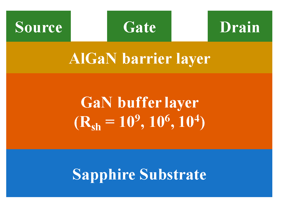
Figure 1.
Schematic illustration of the AlGaN/GaN HEMTs with different GaN buffer resistance (no surface passivation).
Figure 1.
Schematic illustration of the AlGaN/GaN HEMTs with different GaN buffer resistance (no surface passivation).

Figure 2.
(a) Drain currents with double sweep of gate voltage at Vd = 0.1 V and (b) breakdown voltages at Vg = −6 V in the fabricated AlGaN/GaN HEMTs with different GaN buffer resistance.
Figure 2.
(a) Drain currents with double sweep of gate voltage at Vd = 0.1 V and (b) breakdown voltages at Vg = −6 V in the fabricated AlGaN/GaN HEMTs with different GaN buffer resistance.

Figure 3.
(a) Normalized noise spectral density (SId/Id2) according to the frequency and SId/Id2 (black square) matching with (constant × (gm/Id)2) (blue line) versus Id at Vd = 0.1 V and f = 10 Hz for the devices with Rsh = (b) 109, (c) 106, and (d) 104, respectively.
Figure 3.
(a) Normalized noise spectral density (SId/Id2) according to the frequency and SId/Id2 (black square) matching with (constant × (gm/Id)2) (blue line) versus Id at Vd = 0.1 V and f = 10 Hz for the devices with Rsh = (b) 109, (c) 106, and (d) 104, respectively.

Figure 4.
Product SId × frequency versus frequency in the fabricated GaN HEMTs with different GaN buffer resistance at (Vg – Vth) = –1 V and Vd = 0.1 V.
Figure 4.
Product SId × frequency versus frequency in the fabricated GaN HEMTs with different GaN buffer resistance at (Vg – Vth) = –1 V and Vd = 0.1 V.

Figure 5.
Pulsed Id-Vd and Id-Vg curves for the devices with Rsh = (a), (b) 109, (c), (d) 106, and (e), (f) 104 sweeping Vd = 0~10 V.
Figure 5.
Pulsed Id-Vd and Id-Vg curves for the devices with Rsh = (a), (b) 109, (c), (d) 106, and (e), (f) 104 sweeping Vd = 0~10 V.


Table 1.
Structural and electrical properties in AlxGax−1N/GaN high-electron-mobility transistors (HEMTs) with different GaN buffer resistance measured by atomic force microscopy (AFM), Hall effect, and high-resolution X-ray diffraction (HRXRD).
Table 1.
Structural and electrical properties in AlxGax−1N/GaN high-electron-mobility transistors (HEMTs) with different GaN buffer resistance measured by atomic force microscopy (AFM), Hall effect, and high-resolution X-ray diffraction (HRXRD).
| Samples | AFM | Hall Effect | HRXRD | ||||
|---|---|---|---|---|---|---|---|
| Rsh for the GaN Buffer Layer [Ω/sq.] | RMS [nm] | Rsh [Ω/sq.] | μe [cm2/V·s] | ns [cm−2] | Al Composition [%] | GaN FWHM (002) | GaN FWHM (102) |
| 109 (proposed device) | 0.389 | 496 | 1420 | 0.88 × 10¹³ | 25 | 292 | 659 |
| 106 (reference device) | 0.603 | 440 | 515 | 2.75 × 10¹³ | 25 | 299 | 748 |
| 104 (reference device) | 0.466 | 501 | 228 | 5.45 × 10¹³ | 25 | 311 | 745 |
© 2020 by the authors. Licensee MDPI, Basel, Switzerland. This article is an open access article distributed under the terms and conditions of the Creative Commons Attribution (CC BY) license (http://creativecommons.org/licenses/by/4.0/).
Share and Cite
MDPI and ACS Style
Im, K.-S.; Lee, J.-H.; Choi, Y.J.; An, S.J. Effects of GaN Buffer Resistance on the Device Performances of AlGaN/GaN HEMTs. Crystals 2020, 10, 848. https://0-doi-org.brum.beds.ac.uk/10.3390/cryst10090848
AMA Style
Im K-S, Lee J-H, Choi YJ, An SJ. Effects of GaN Buffer Resistance on the Device Performances of AlGaN/GaN HEMTs. Crystals. 2020; 10(9):848. https://0-doi-org.brum.beds.ac.uk/10.3390/cryst10090848
Chicago/Turabian StyleIm, Ki-Sik, Jae-Hoon Lee, Yeo Jin Choi, and Sung Jin An. 2020. "Effects of GaN Buffer Resistance on the Device Performances of AlGaN/GaN HEMTs" Crystals 10, no. 9: 848. https://0-doi-org.brum.beds.ac.uk/10.3390/cryst10090848
Note that from the first issue of 2016, this journal uses article numbers instead of page numbers. See further details here.