Article

High-Drain Field Impacting Channel-Length Modulation Effect for Nano-Node N-Channel FinFETs

1
Department of Electronic Engineering, Minghsin University of Science and Technology, Hsinchu 30401, Taiwan
2
Department of Electro-Optical Engineering, Minghsin University of Science and Technology, Hsinchu 30401, Taiwan
3
Department of Mechanical Engineering, National Taipei University of Technology, Taipei 10608, Taiwan
4
Department of Mechanical Engineering, Minghsin University of Science and Technology, Hsinchu 30401, Taiwan
5
Department of Electrical Engineering, National University of Kaohsiung, Kaohsiung 81148, Taiwan
*
Authors to whom correspondence should be addressed.
Submission received: 27 January 2021 / Revised: 27 February 2021 / Accepted: 5 March 2021 / Published: 7 March 2021
(This article belongs to the Section Crystal Engineering)

Abstract

:
Three dimensional (3-D) FinFET devices with an ultra-high Si-fin aspect ratio have been developed after integrating a 14Å nitrided gate oxide upon the silicon on insulator (SOI) wafers through an advanced CMOS logic platform. Under the lower gate voltage (VGS-VT) and the higher drain/source voltage VDS, the channel-length modulation (CLM) effect coming from the interaction impact of vertical gate field and horizontal drain field was increased and had to be revised well as the channel length L was decreased. Compared to the 28-nm MOSFETs, the interaction effect from the previous at the tested FinFETs on SOI substrate with the short-channel length L is lower than that at the 28-nm device, which means the interaction severity of both fields for nFinFETs is mitigated, but still necessary to be concerned.

1. Introduction

With the evolution of process technology and the need of marketing, exploring the high speed, low cost, and high-volume capacity in integrated-circuit (IC) chips is the development trend in the modern semiconductor industry [1,2,3]. As the process of technology enters the nano-node generation, seeking the better device structure compatible with the Si-based process flow is a good way to promote the drive current and product competition. The fin field-effect transistor (FinFET) structure is one of the impressive candidates in the tremendous competitive FET devices [4,5,6,7]. In order to obtain ultra-high density metal-oxide-semiconductor FET-like (MOSFET) IC products, a 3D FinFET device has been incorporated as a promising candidate as compared to other double gate device structures [8,9] owing to its process compatibility with conventional logic devices. Furthermore, FinFET devices demonstrate the advantages of avoiding the shallow trench isolation process as well as effective improvement of drive current ION, device leakage IOFF, subthreshold swing, drain-induced barrier lowing (DIBL) effect, and short channel effect (SCE) due to the good controllability of gate electrode surrounding the erected silicon body of Si-fin [10,11]. Besides the substrate with silicon bulk substrate [12,13], the device fabricated by adopting the silicon-on-insulator (SOI) wafer [14,15] in high-performance computing (HPC) products including the advanced 5G/6G communication systems, smart phones, quantum calculation, artificial intelligent applications, and driverless systems are a feasible choice [16,17,18]. Using the SOI wafer, the benefits for IC chips compared with the conventional bulk silicon substrate chiefly contain lower supply power which can reduce power by 2 to 3 times, high performance which reduces switching delays and gains the improvement of 20% to 30% in speed, soft error rate and radiation hard reduced because the FET devices are isolated from substrate [19,20]. Moreover, HPC products adopting FinFET devices usually operate at the high-frequency or microwave range [21,22], the complication of IC design is increased more, including the noise issue [23,24].
Consequently, besides the improvement of physical process development, the precise simulators for IC design houses are indeed necessary to make sure IC production is successful because each investment of nano-node IC products is over a couple million US dollars or more. With the accurate sets of intellectual property (IP), the successful rate in IC design is possible and hugely raised. Hence, providing a set of accurate device models bridging the foundry and the design houses in the nano-node era with fin-Si structure is an important contribution. Due to this effort, in addition to promoting the drive current [25] and indirectly increasing the operation speed, the reliable device models consolidating the process and device simulation software will enhance the stability of circuit operation. In the past, some researchers studied the device model with early voltage [26,27,28,29] causing from the channel-length modulation effect at the 28-nm process technology with traditional bulk wafers. However, the device model is chiefly focused on the higher vertical field at the gate electrode. The model of the early effect under the low-field operation was not described well. To compensate this insufficiency, this study will entirely probe the early effect on the single-fin and multi-fin FinFETs with some various channel-length devices, as shown in Figure 1. Adopting the multi-fin FinFETs to possibly reduce series resistance and source/drain-to-gate capacitance, the source/drain current IDS is also increased more, but not unlimited and linearly increased with the increase of fin number [30,31,32]. One of the possible causes is that the micro-loading effect in the etching process is more distinct, especially in the high aspect ratio of fin height/fin channel width. The other side effect for the increment of fin number degrades the performance of device reliability such as in the hot-carrier stress [33] because carrier conduction in the steep Si fins of FinFETs is different for a device with multiple number of fins and probably affects device performance and reliability. In general, the unsuitable device models will influence the accuracy of circuit performance in simulation and real operation [34]. Thus, seeking the more accurate device model [35,36] is the main task in this study. In this case, the contours of the tested FinFETs are the channel width/the channel length (W/L) on mask: 0.12/0.10, 0.12/0.24, and 0.12/0.50 (μm/μm) as well as one and eleven fins.

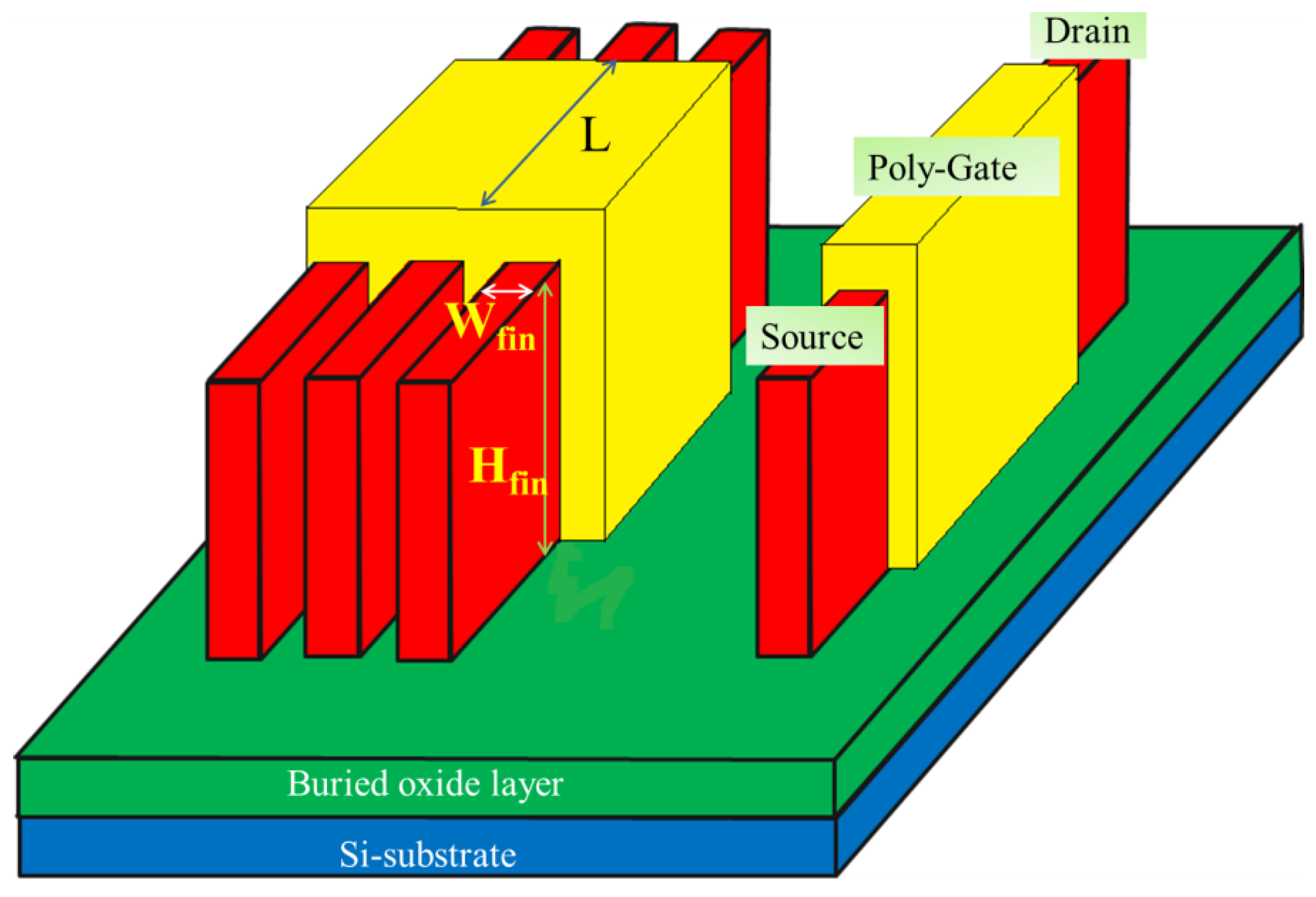
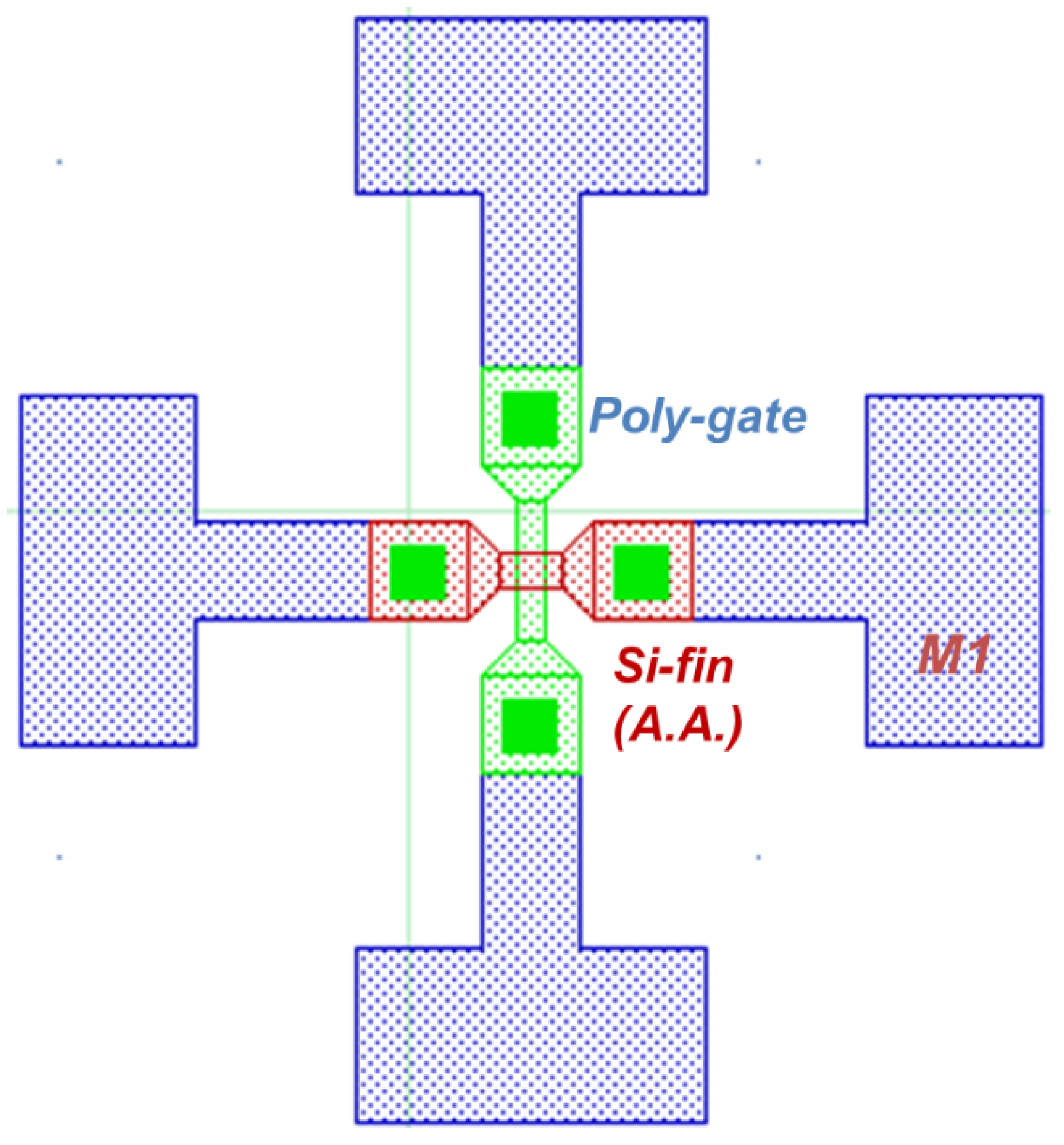
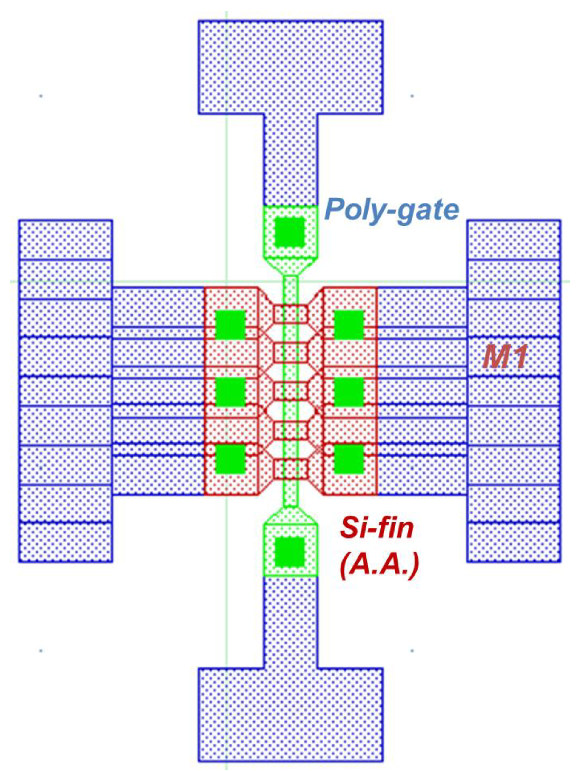
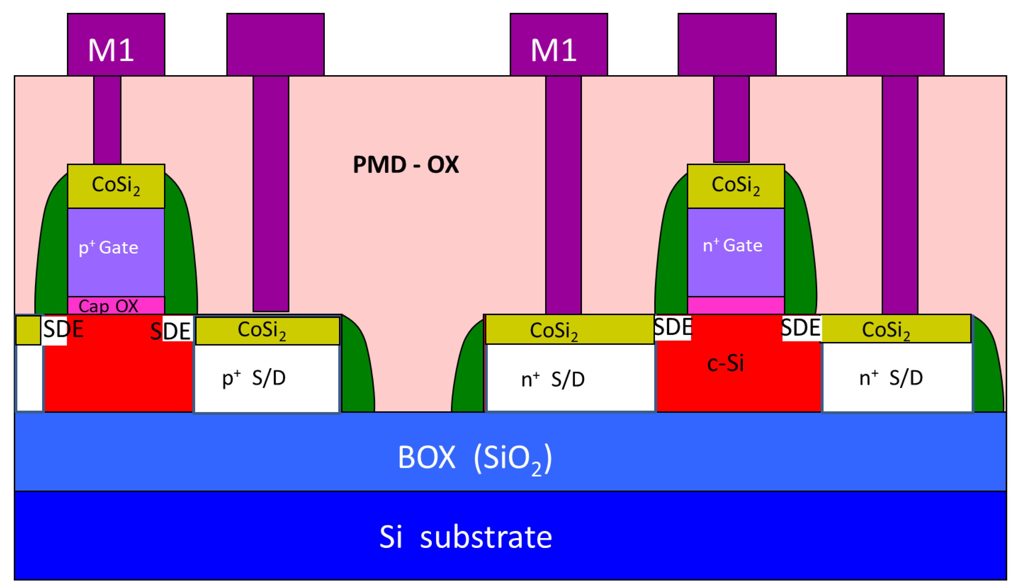
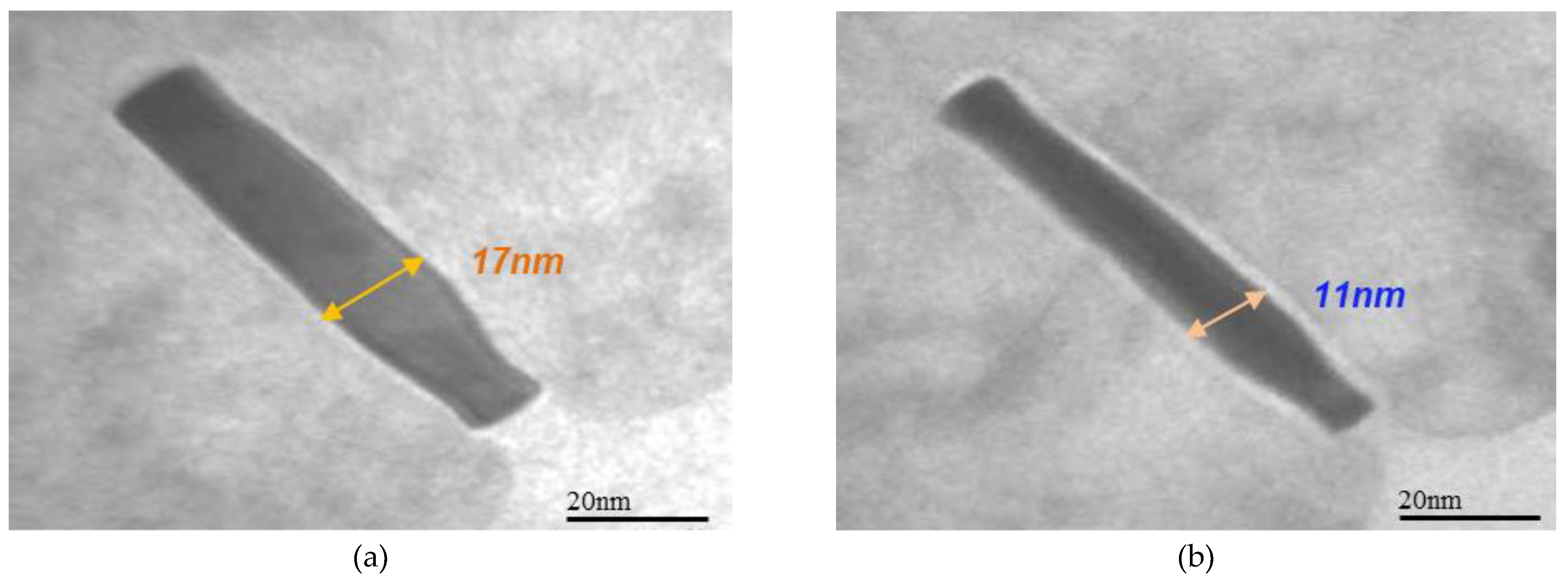
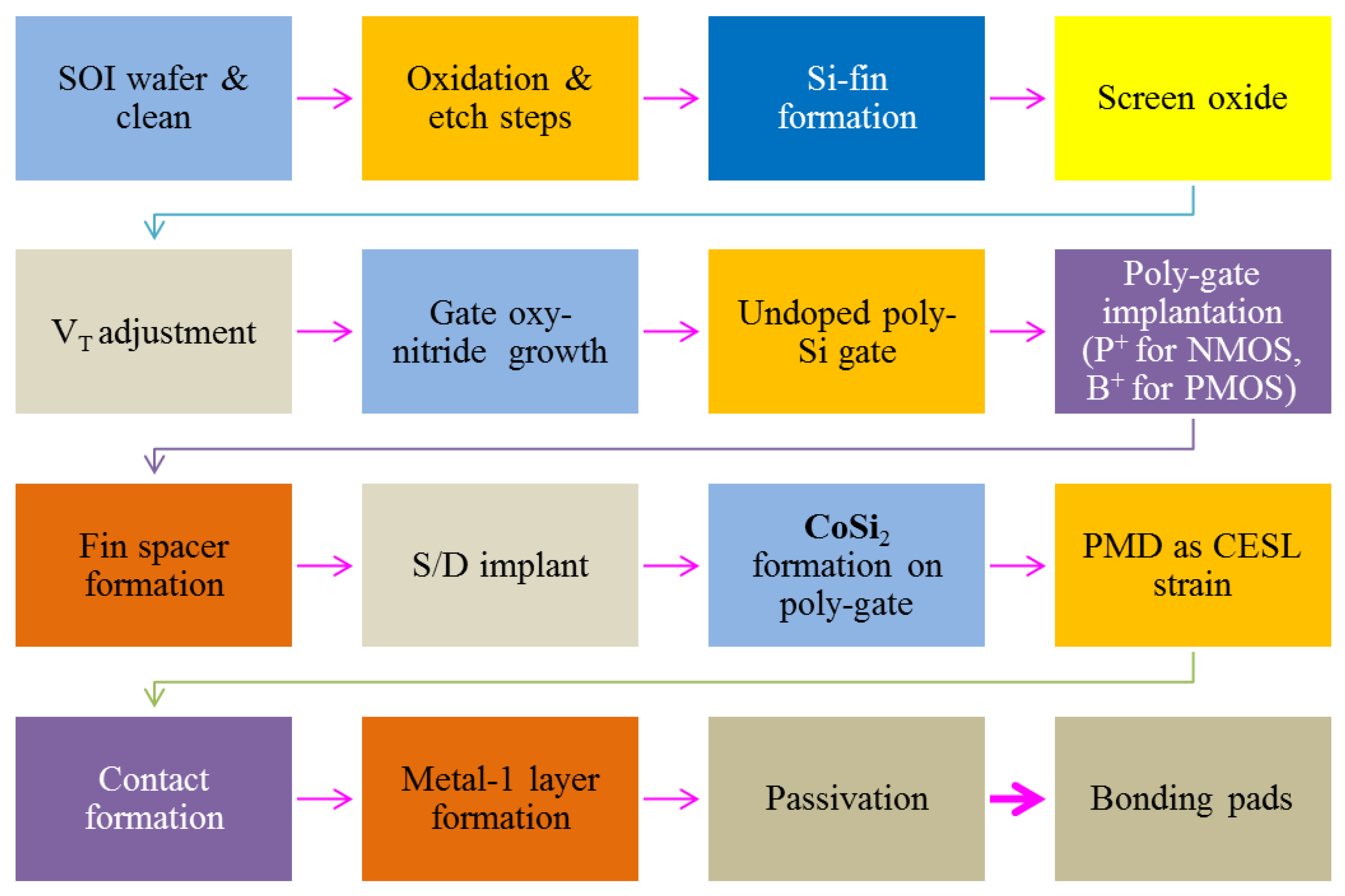
2. Brief Illustration of Device Formation

Designing a set of device layout patterns following the design rules is necessary to probe the accuracy of process flow and device performance, as shown in Figure 2 and Figure 3. Furthermore, the SOI wafers before the definition of the active area were well done in preparation and clean. Continuously, the location and implantation of N/P-well was defined and processed, respectively. With photo-lithography and etch technology, the Si-fin shape was formed. The threshold-voltage implants (VT implant) for n-channel and p-channel FinFETs [37,38] were executed to determine the adequate VT values. Applying the photo lithography and etch process, the desired gate patterns with 11-nm channel width under the over-exposure and adequate etch assistant were obtained. The fin height was about 87 nm [39]. The nitrided oxide with the physical thickness 14Å played as a gate oxide was grown [40,41] as a cap oxide. The undoped poly-Si with epitaxy technology of a chemical vapor deposition (CVD) method was deposited on the gate oxide. The source/drain extension (SDE) implants for n/p-FinFETs were followed to form a protection shield against the hot-carrier effect (HCE) [42]. Consequently, the spacer was deposited to the designed thickness. The source/drain (S/D) implants for both type of FinFETs, and beneficial for the poly-gate conduction, were conducted, respectively. On the heels of the anterior process, the cobalt-silicide process [43] was adopted to reduce the contact resistant and avoid the contact spiking.
Continuously, with strain technology processes [44,45] is helpful to the increase of channel mobility. Following the sub-65nm conventional CMOS process until M1 layer, the front-end FinFETs were completely manufactured. In the end, the back-end of line (BEOL) processes [46,47] including the signal connection patterns, passivation deposition, and contact window were step by step followed up to protect the whole devices and extract the electrical characterization of the devices. The simple cross-section of a complementary n/p-channel FinFET is demonstrated in Figure 4. The cross-sectional TEM (transmission electron microscope) photos with single Si-fin under different photo exposure energy are as shown in Figure 5. The top-view SEM (scanning electron microscope) photos for multi Si-fin and single Si-fin are exhibited in Figure 6 and the concise process flow is denoted in Figure 7.

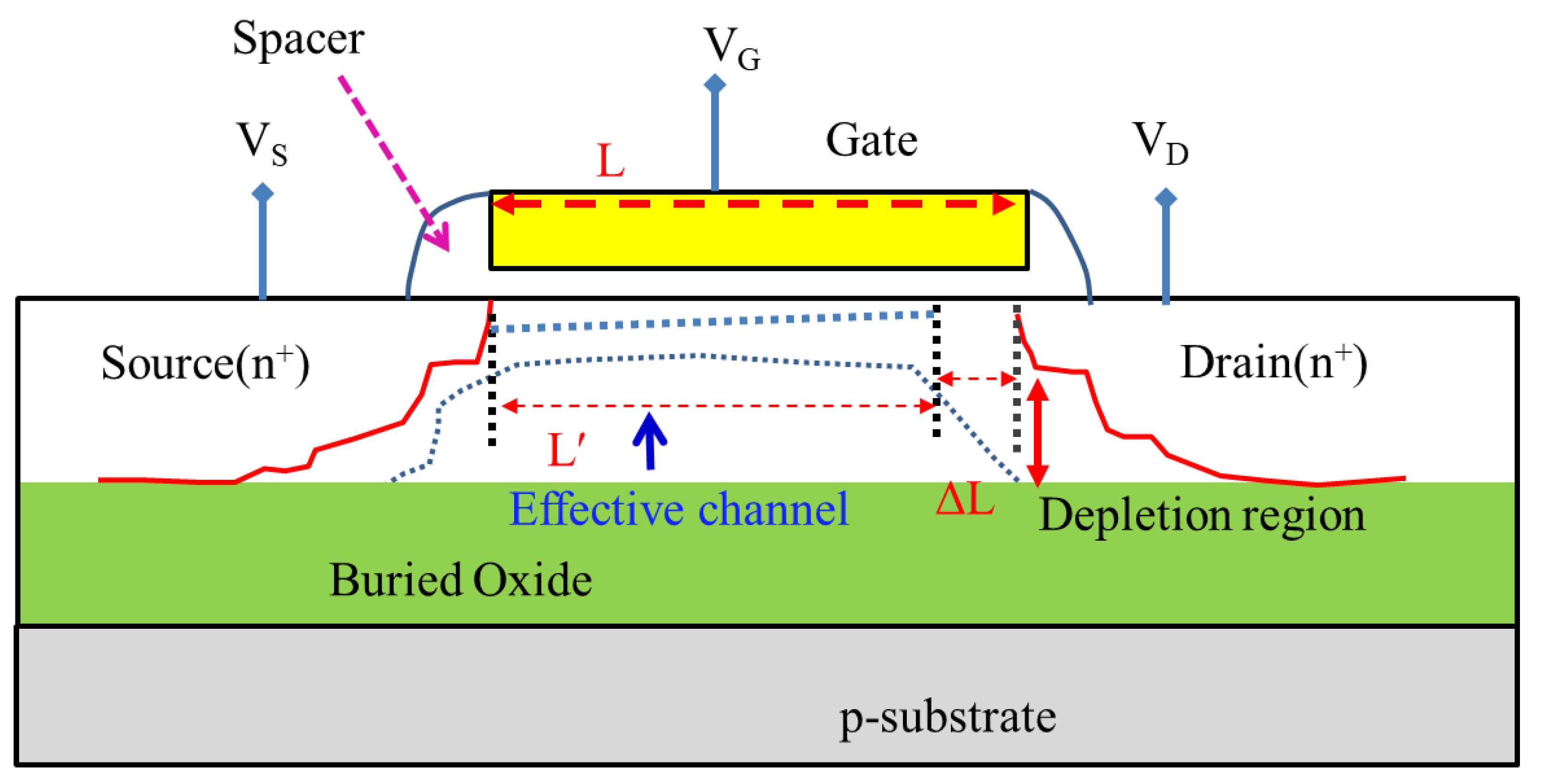
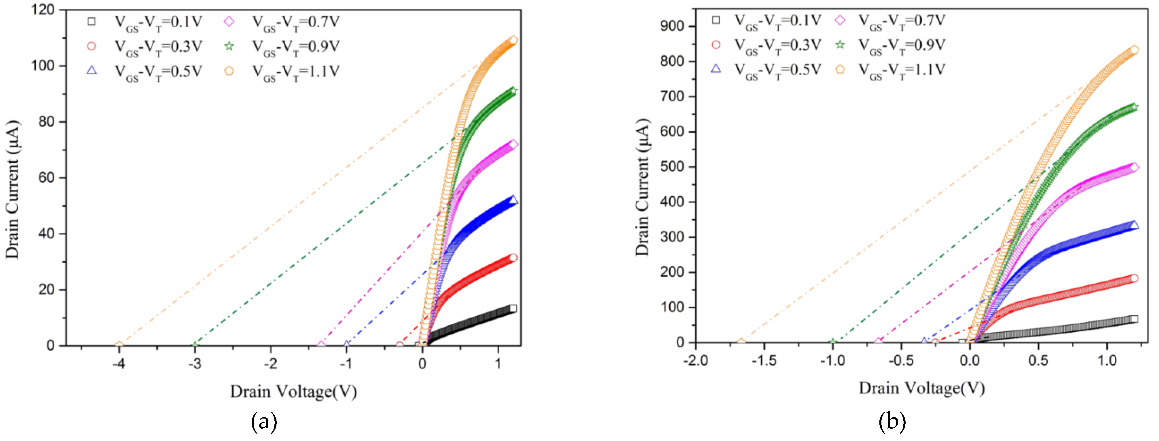
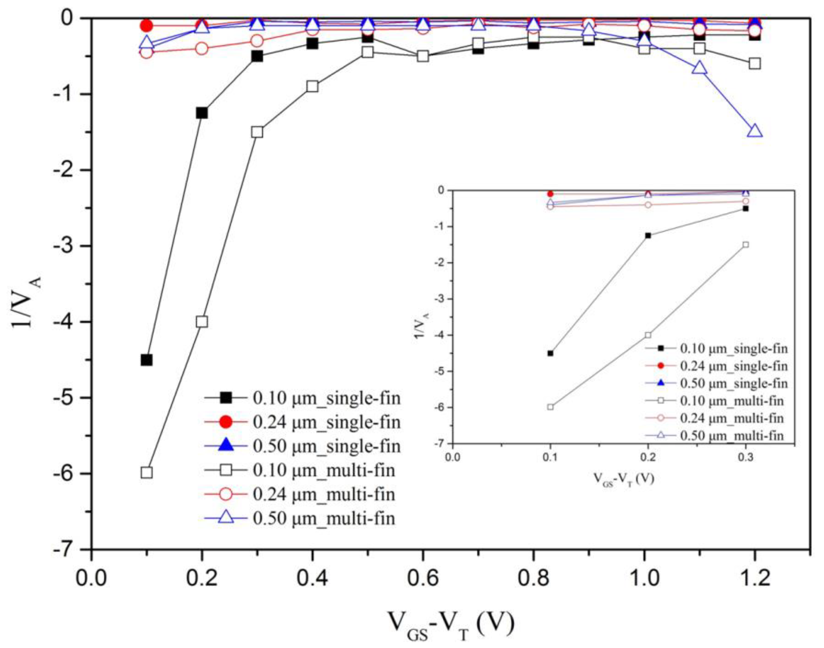
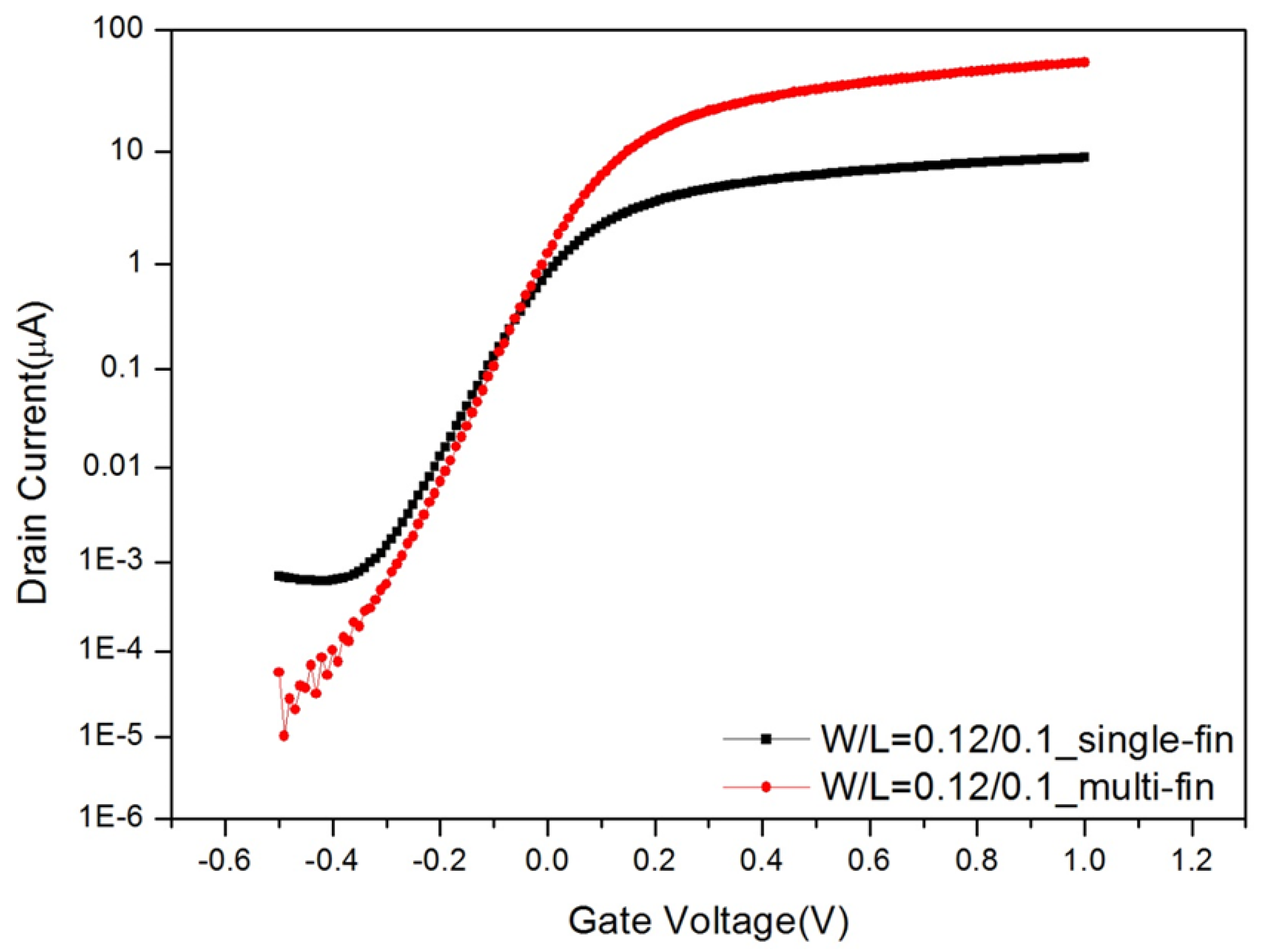
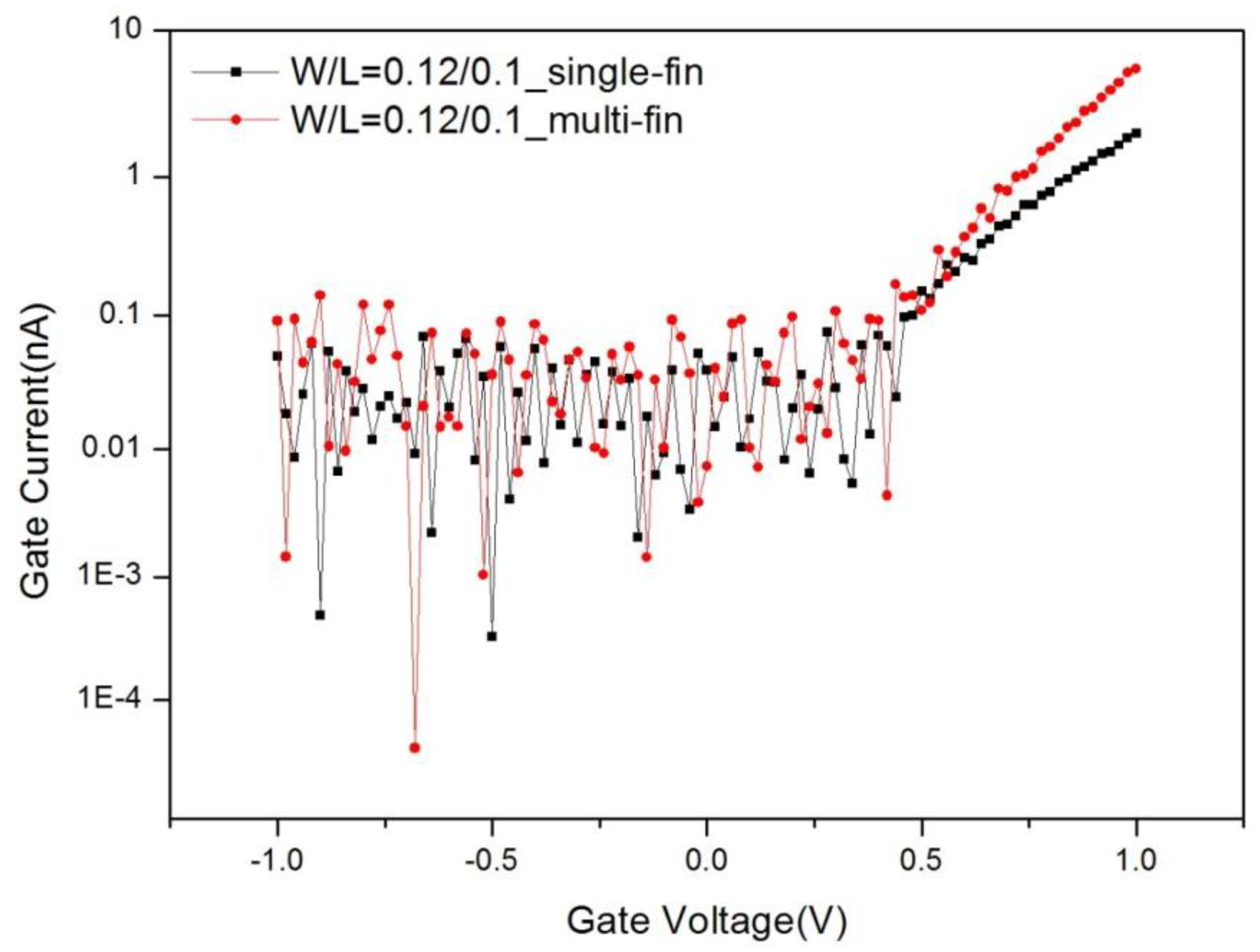
3. Results and Discussion

For an n-channel FinFET (nFinFET), the drive current (IDS) at the saturation mode can be represented as Equation (1) [28,29]:
I D S W t 2 m L μ n C o x ( V G S V T ) 2 ( 1 + Δ L L ) ,
where Wt: total channel width = fin channel width + 2 fin height = Wfin + 2 Hfin, L: channel length, m: body effect factor, μn: channel mobility, Cox: gate capacitance per area at the inversion mode, VGS: gate/source voltage, ∆L: pinch-off region, as shown in Figure 8.
In the past, the ∆L/L was only described to relate the horizontal field VDS. It could be represented as Equation (2):
Δ L L λ V D S ,
where λ is the channel length modulation factor as 1/VA and VA is the early voltage.
When we consider the vertical contribution, Equation (2) may be modified as Equation (3):
Δ L L λ V D S + α ( V G S V T ) + β ( V G S V T ) V D S ,
where α and β are also the channel length modulation factors related to the vertical field and the mutual-interaction between both, respectively. The effective channel length L’ is defined as (L−∆L).
One of the measured results for the electrical characteristics of the S/D currents vs. VGS-VT or VDS with W/L = 0.12/0.10 (μm/μm) on mask at room temperature is shown in Figure 9. Generally, the multi-fin FinFET is to increase the drive current compared with the single FinFET or 2-D MOSFET due to the multi-channel or the increment of fin height increasing the whole channel gate width and drive current. The intercept voltage operated at each VGSVT indicates the early voltage (VA). When the vertical field (VGSVT) operated is lower and fixed and the VDS is higher, Equation (3) can be simplified as ∆L/L ≈ [λ + β(VGSVT)]VDS, which means the minor contribution of α(VGS–VT) is able to be ignored because of comparing the other terms in the right-hand side of Equation (3) in this assumption. For the different channel lengths, the extracted values for λ and β are listed at Table 1Table 2Table 3 and Table 4. The distribution of β-values can be treated as two mechanisms. In Table 1 and Table 2, the vertical field is lower and the β-value linearly plays a slope of 1/VA vs. (VGSVT), as shown in Figure 10. Reversely, it is higher in Table 3 and Table 4 and the contribution of β-value is hugely reduced. We suggest that when the higher drain and gate fields are applied, the carrier transport mechanism in channel is not pure to be explained with the uniform charge distribution, but includes the quantum mechanical effect [29] and the ballistic transport with Boltzmann distribution [48].
Through the decrease of the channel lengths, the β-factor is increased, especially at the shortest one which means the contribution coming from the vertical field is more distinct [49]. As the establishment of the device models at the short channel part, this vertical effect dominating the accurate model must be of concern more than before. Comparing the extracted consequence for β-factor with Reference 26 (β ≈ 1.4~1.6), the β-factor for the FinFET at the long-channel device is a little higher than that at the 28-nm MOSFETs. As the device channel length is narrowed down, the vertical-field contribution to the drive current is gradually increased, as shown in Figure 10. On the contrary, when the VDS and the VGSVT are higher, the β-factor at FinFETs with short-channel device is less than that at Reference 26, as shown at Table 3 and Table 4. There is a turning point observed at the L = 0.24 μm, showing the minimum value owing to the bias of photo-lithography. This channel-length modulation should be adjusted and the β-factor must be extracted carefully. For the multi-fin device, the process issues are also possible to influence the electrical performance. For instance, the micro-loading effect for the multi-fin devices in etching process technology is a tremendous challenge, affecting the etching performance and probably causing the expected aspect ratio of fin height/ fin channel width, which cannot be approached. In spite of this, using the β value to justify the etching performance in different multi-fin structures can be treated as an extra benefit in process monitoring. In addition to the foregoing lithography [50] and dry etch [51] impacting the roughness and uniformity of Si-fin strongly correlated to the β-factor, the ion doping factors including the doping energy, doping dosage, and dopant species in adjustment of threshold implantation will probably influence the β-factor. Hence, each novel or changed process flow will follow a new set of device models.
The related electrical characteristics of IDS vs. VGS and IGS vs. VGS for the tested device with W/L = 0.12/0.1 (μm/μm) are demonstrated in Figure 11 and Figure 12, respectively. The measurement equipment is Keysight B1500A which can provide the accuracy current range until fA (10−15 A) level. The threshold swings (SS) for single and multi-fin FinFETs are 96 and 85 mV/decade, respectively. These electrical performances in device design are acceptable although the SS value for single fin is a little higher, which is still less than 100 mV/decade. Because the SS value is an index to illustrate the capability of ON/OFF speed of FinFETs. As the single and multi-fin FinFETs are scanned by the gate bias, the multi-fin device usually provides more drive current than the single one. Hence, we suggest that the swing capability of the multi-fin device should be better than that of the single one.
Concerning the contribution of plasma etching with micro-loading effect, the main effort focused on the multi-fin contour. The interface integrity of single FinFET on the channel surface has been suffered a little more. The gate leakage in accumulation mode as source/drain grounded is low like noise and in inversion mode is gradually raised up as VGS is positively increased. The speculation is that because the substrate of tested devices is SOI-type floating, not bulk-type, the channel potential for the tested device is unstable at the accumulation mode. Thus, the gate leakage in measurement is treated as noise. However, as the SOI devices are biased at the inversion mode, the channel potential is grounded with source/drain electrodes. Hence, the pseudo noise issue is reduced more and the gate leakage is truly responding. In the future, the simulator provides not only the simulation functions of process and device, but the reliability functions together. In reliability concern, the electrical performance in devices or IC shifting is 10% in operating or thermal stress is treated as a failed sample. Thus, providing an accurate set of device models is urgently needed at the sub-28-nm node, which can shorten the IC development time, advance the yield of IC products, and save more money in the entire project.

4. Conclusions

Considering the 3-D FinFET device upon SOI wafer with an ultra-thin Si-fin, it is indeed feasible to be employed to deep sub-nano process technology such as the sub-14-nm node [52,53,54]. Before the high-k dielectric integrated into HPC IC products or the low-cost consideration, providing the oxy-nitride (SiON) dielectric as gate dielectric is still an adoptable way to temporarily satisfy the need of IC design houses. In this article, while the FET device is narrowed down, the device model in channel-length modulation becomes more complicated owing to the contribution of the vertical gate field. In these tested FinFETs, we observed that the β-factor illustrating the contribution of the vertical field was increased as the channel length decreased at the higher VDS and lower VGS-VT case. For both at the higher, the trend of the β-factors with the channel lengths were reverse. Using these consequences incorporating into the device model beneficially improving the device performance at the sub-28-nm node is desirably expected. Furthermore, this kind of application in model improvement also can be extended to gate-all-around (GAA) FETs or multi-bridge-channel (MBC) FETs for sub-7-nm manufacturing technology [55,56,57] or other FET-like devices [58].

Author Contributions

Conceptualization, M.C.W.; methodology, W.C.H.; formal analysis, C.R.L., W.S.L., and W.S.L.; data curation, W.L.C.; writing—original draft preparation, M.C.W.; writing—review and editing, W.C.H., W.S.L. and W.H.L.; project administration, C.R.L. All authors have read and agreed to the published version of the manuscript.

Funding

This research received no external funding.

Institutional Review Board Statement

The study was conducted according to the guidelines of the Declaration of Helsinki, and approved by the Institutional Review Board.

Informed Consent Statement

Informed consent was obtained from all subjects involved in the study.

Data Availability Statement

Not applicable.

Acknowledgments

The authors sincerely appreciate United Microelectronics Corporation in Taiwan for supporting 8” SOI wafers, and the financial support from Ministry of Science and Technology of Republic of China under Contract Nos. MOST 109-2622-E-159-001.

Conflicts of Interest

The authors declare no conflict of interest.

References

  1. Xiao, H. Introduction to Semiconductor Manufacturing Technology, 2nd ed.; SPIE: Washington, DC, USA, 2012; pp. 1–93. [Google Scholar]
  2. Dosi, G. Technical Change and Industrial Transformation: The theory and an Application to Semiconductor Industry, 1st ed.; Macmillan Press: London, UK, 1984; pp. 100–200. [Google Scholar]
  3. Baldauf, T.; Wei, A.; Illgen, R.; Flachowsky, S.; Herrmann, T.; Höntschel, J.; Horstmann, M.; Klix, W.; Stenzel, R. Study of 22/20 nm trigate transistors compatible in a low-cost hybrid FinFET/planar CMOS process. In Proceedings of the IEEE ISDRS, College Park, MD, USA, 7–9 December 2011. [Google Scholar]
  4. Pham, D.; Larson, L.; Yang, J. FinFET device junction formation challenges. In Proceedings of the IEEE IWJT, Shanghai, China, 15–16 May 2006. [Google Scholar]
  5. LaPedus, M. Transistor Options beyond 3 nm. Semicond. Eng., Feb. 2018. Available online: https://semiengineering.com/transistor-options-beyond-3nm/ (accessed on 3 January 2021).
  6. Vidya, S.; Kamat, S.; Khan, A.; Venkatesh, V. 3D FinFET for next generation nano devices. In Proceedings of the IEEE ICCTCT, Coimbatore, Tamil Nadu, India, 1–3 March 2018. [Google Scholar]
  7. Razavieh, A.; Zeitzoff, P.; Nowak, E. Challenges and limitations of CMOS scaling for FinFET and beyond architectures. IEEE Trans. Nanotech. 2019, 18, 999–1004. [Google Scholar] [CrossRef]
  8. Hisamoto, D.; Lee, W.C.; Kedzierski, J.; Takeuchi, H.; Asano, K.; Kuo, C.; Anderson, E.; King, T.J.; Bokor, J.; Hu, C. FinFET-a self-aligned double-gate MOSFET scalable to 20 nm. IEEE Trans. Electron Dev. 2000, 47, 2320–2325. [Google Scholar]
  9. Wong, H.S.P.; Chan, K.K.; Taur, Y. Self-aligned (top and bottom) double-gate MOSFET with a 25 nm thick silicon channel. In Proceedings of the IEEE IEDM, Washington, DC, USA, 10 December 1997. [Google Scholar]
  10. El-Mamouni, F.; Zhang, E.X.; Ball, D.R.; Sierawski, B.; King, M.P.; Schrimpf, R.D.; Reed, R.A.; Alles, M.L.; Fleetwood, D.M.; Linten, D.; et al. Heavy-ion-induced current transients in bulk and SOI FinFETs. IEEE Trans. Nucl. Sci. 2012, 59, 2674–2681. [Google Scholar] [CrossRef]
  11. Li, Y.; Hwang, C.H. Effect of fin angle on electrical characteristics of nanoscale round-top-gate bulk FinFETs. IEEE Trans. Electron Dev. 2007, 54, 3426–3429. [Google Scholar] [CrossRef]
  12. Han, M.H.; Chang, C.Y.; Chen, H.B.; Cheng, Y.C.; Wu, Y.C. Device and circuit performance estimation of junctionless bulk FinFETs. IEEE Trans. Electron Dev. 2013, 60, 1807–1813. [Google Scholar] [CrossRef]
  13. Mittl, S.; Guarín, F. Self-heating and its implications on hot carrier reliability evaluations. In Proceedings of the IEEE IRPS, Monterey, CA, USA, 19–23 April 2015. [Google Scholar]
  14. Poljak, M.; Jovanovic, V.; Suligoj, T. SOI vs. bulk FinFET: Body doping and corner effects influence on device characteristics. In Proceedings of the IEEE MELECON, Ajaccio, France, 5–7 May 2008. [Google Scholar]
  15. Aziz, M.N.I.A.; Salehuddin, F.; Mohd Zain, A.S.; Kaharudin, K.E.; Radzi, S.A. Comparison of electrical characteristics between bulk MOSFET and silicon-on-insulator (SOI) MOSFET. J. Telecom. Electron. Comp. Eng. 2014, 6, 45–49. [Google Scholar]
  16. Krivec, S.; Prgić, H.; Poljak, M.; Suligoj, T. Comparison of RF performance between 20 nm-gate bulk and SOI FinFET. In Proceedings of the IEEE MIPRO, Opatija, Croatia, 26–30 May 2014. [Google Scholar]
  17. Ernst, T.; Tinell, C.; Raynaud, C.; Cristoloveanu, S. Fringing fields in sub-0.1 μm fully depleted SOI MOSFETs: Optimization of the device architecture. Solid State Electron. 2002, 46, 373–378. [Google Scholar] [CrossRef]
  18. Cristoloveanu, S. Silicon on insulator technologies and devices: From present to future. Solid State Electron. 2001, 45, 1403–1411. [Google Scholar] [CrossRef]
  19. Deshmukh, R.; Khanzode, A.; Kakde, S.; Shah, N. Compairing FinFETs: SOI vs. Bulk: Process variability, process cost, and device performance. In Proceedings of the IEEE IC4, Indore, India, 10–12 September 2015. [Google Scholar]
  20. Godara, M.; Madhu, C.; Joshi, G. Comparison of electrical characteristics of 28 nm bulk MOSFET and FDSOI MOSFET. In Proceedings of the IEEE EDKCON, Kolkata, India, 24–25 November 2018. [Google Scholar]
  21. Lederer, D.; Kilchytska, V.; Rudenko, T.; Collaert, N.; Flandre, D.; Dixit, A.; De Meyer, K.; Raskin, J.-P. FinFET analogue characterization from DC to 110 GHz. Solid State Electron. 2005, 49, 1488–1496. [Google Scholar] [CrossRef]
  22. Crupi, G.; Schreurs, D.M.M.-P.; Caddemi, A.; Angelov, I.; Homayouni, M.; Raffo, A.; Vannini, G.; Parvais, B. Purely analytical extraction of an improved nonlinear FinFET model including non-quasi-static effects. Microelectron. Eng. 2009, 86, 2283–2289. [Google Scholar] [CrossRef]
  23. Raskin, J.P.; Pailloncy, G.; Lederer, D.; Danneville, F.; Dambrine, G.; Decoutere, S.; Mercha, A.; Parvais, B. High-frequency noise performance of 60-nm gate-length FinFETs. IEEE Trans. Electron Dev. 2008, 55, 2718–2727. [Google Scholar] [CrossRef]
  24. Crupi, G.; Caddemi, A.; Schreurs, D.M.M.-P.; Wiatr, W.; Mercha, A. Microwave noise modeling of FinFETs. Solid State Electron. 2011, 56, 18–22. [Google Scholar] [CrossRef]
  25. Neamen, D.A. An Introduction to Semiconductor Devices, 1st ed.; McGraw-Hill: New York, NY, USA, 2006; pp. 223–357. [Google Scholar]
  26. Lee, W.D.; Wang, M.C.; Wang, S.J.; Lan, W.H.; Li, C.W.; Yang, B.W. Modification of Early effect for 28-nm nMOSFETs deposited with HfZrOx dielectric after DPN process accompanying nitrogen concentrations. IEEE Trans. Plasma Sci. 2014, 42, 3747–3750. [Google Scholar] [CrossRef]
  27. Yang, H.C.; Du, C.K.; Liao, W.S.; Jhang, J.Z.; Lee, Y.H.; Chen, T.Y.; Liao, K.F.; Wang, M.C.; Chi, S.; Wang, S.J. The side effects on n-type FinFET device. In Proceedings of the IEEE INEC, Singapore, 2–4 January 2013. [Google Scholar]
  28. Streetman, B.G. , Banerjee, S.K. Solid State Electronic Devices, 7th ed.; Pearson: Hoboken, NJ, USA, 2016; pp. 280–350. [Google Scholar]
  29. Hu, C. Modern Semiconductor Devices for Integrated Circuits, 1st ed.; Pearson: Hoboken, NJ, USA, 2010; pp. 175–307. [Google Scholar]
  30. Shang, H.; Chang, L.; Wang, X.; Rooks, M.; Zhang, Y.; To, B.; Babich, K.; Totir, G.; Sun, Y.; Kiewra, E.; et al. Investigation of FinFET devices for 32 nm technologies and beyond. In Proceedings of the IEEE VLSIT, Honolulu, HI, USA, 13–15 January 2006. [Google Scholar]
  31. Wangm, X.; Bryantm, A.; Dokumacim, O.; Oldigesm, P.; Haenschm, W. Simulation study of multiple fin FinFET design for 32 nm technology node and beyond. In Simulation of Semiconductor Processes and Devices 2007; Springer: Vienna, Austria, 2007. [Google Scholar] [CrossRef] [Green Version]
  32. Avushyan, S.; Petrosyan, K.; Kaplanyan, T.; Shaljyan, D.; Mikaelyan, L.; Shukhyan, N.; Momjyan, A. Current scaling of multi-fin devices in FinFET process. In Proceedings of the IEEE ELNANO, Kyiv, Ukraine, 16–18 April 2019. [Google Scholar]
  33. Yeh, W.; Zhang, W.; Chen, P.; Yang, Y. The impact of fin number on device performance and reliability for multi-fin tri-gate n- and p-type FinFET. IEEE Trans. Dev. Mater. Reliab. 2018, 18, 555–560. [Google Scholar] [CrossRef]
  34. Wang, F.; Xie, Y.; Bernstein, K.; Luo, Y. Dependability analysis of nano-scale FinFET circuits. In Proceedings of the IEEE ISVLSI, Karlsruhe, Germany, 2–3 March 2006. [Google Scholar]
  35. Lu, D.; Dunga, M.; Niknejad, A.; Hu, C.; Liang, F.; Hung, W.; Lee, J.; Hsu, C.; Chiang, M. Compact device models for FinFET and beyond. In Proceedings of the AWAD, Kitakyushu, Japan, 2–4 July 2018; Available online: http://arXiv:2005.02580 (accessed on 3 January 2021).
  36. Chauhan, Y.; Lu, D.; Vanugopalan, S.; Khandelwal, S.; Duarte, J.; Paydavosi, N.; Niknejad, A.; Hu, C. FinFET Modeling for IC Simulation and Design, 1st ed.; Academic Press: Cambridge, MA, USA, 2015; pp. 72–96. [Google Scholar] [CrossRef]
  37. Kim, S.; Kim, J.; Jang, D.; Ritzenthaler, R.; Parvais, B.; Mitard, J.; Mertens, H.; Chiarella, T.; Horiguchi, N.; Lee, J. Comparison of temperature dependent carrier transport in FinFET and gate-all-around nanowire FET. Appl. Sci. 2020, 10, 2979. [Google Scholar] [CrossRef]
  38. Khan, T.E.A.; Sheena, S.; Hameed, T.A.S. An investigation on the effect of LER on threshold voltage and On Current of SOI, bulk and GAA FinFETs. In Proceedings of the IEEE ICETIETR, Ernakulam, India, 11–13 July 2018. [Google Scholar]
  39. Liao, W.S. A high aspect ratio Si-fin FinFET fabricated with 193 nm scanner photolithography and thermal oxide hard mask etching techniques. In Proceedings of the SPIE 6156, San Jose, CA, USA, 14 March 2006. [Google Scholar]
  40. Liao, W.S.; Liaw, Y.G.; Tang, M.C.; Chakraborty, S.; Liu, C.W. Investigation of reliability characteristics in NMOS and PMOS FinFETs. IEEE Electron Dev. Lett. 2008, 29, 788–790. [Google Scholar] [CrossRef]
  41. Liaw, Y.G.; Liao, W.S.; Wang, M.C.; Lin, C.L.; Zhou, B.; Gu, H.; Li, D.; Zou, X. A high aspect ratio silicon-fin FinFET fabricated upon SOI wafer. Solid State Electron. 2016, 126, 46–50. [Google Scholar] [CrossRef]
  42. Han, J.W.; Lee, C.H.; Park, D.; Choi, Y.K. Parasitic S/D resistance effects on hot-carrier reliability in body-tied FinFETs. IEEE Electron Dev. Lett. 2006, 27, 514–516. [Google Scholar]
  43. Elgomati, H.A.; Majlis, B.Y.; Salehuddin, F.; Ahmad, I.; Zaharim, A.; Hamid, F.A. Cobalt silicide and titanium silicide effects on nano devices. In Proceedings of the IEEE RSM, Kota Kinabalu, Malaysia, 28–30 September 2011. [Google Scholar]
  44. Xu, Q.; Xiong, W.; Wang, G.; Ye, T. Stressor SiNx contact etch stop layer (CESL) technology and its application in nano-scale transistors. J. Mater. Sci.: Mater. Electron. 2020, 31, 10078–10083. [Google Scholar] [CrossRef]
  45. Dash, T.; Dey, S.; Das, S.; Mohapatra, E.; Jena, J.; Maiti, C. Strain-engineering in nanowire field-effect transistors at 3 nm technology node. Phys. E Low dim. Syst. Nanostr. 2020, 118, 113964. [Google Scholar] [CrossRef]
  46. Voisin, S.; Knopik, V.; Forest, J.; Kerhervé, E. A 65 nm CMOS SOI 4-bit digitally controlled variable gain amplifier for Ka-band beamforming. In Proceedings of the IEEE EuMIC, Utrecht, Netherlands, 10–15 January 2021. [Google Scholar]
  47. Shauly, E.N. Physical, electrical, and reliability considerations for copper BEOL layout design rules. J. Low Power Electron. Appl. 2018, 8, 20. [Google Scholar] [CrossRef] [Green Version]
  48. Fiori, G.G.; Iannaccone, G. The effect of quantum confinement and discrete dopants in nanoscale 50 nm nMOSFETs: A three-dimensional simulation. Nanotechnology 2002, 13, 294–297. [Google Scholar] [CrossRef]
  49. Schulz, T.; Xiong, W.; Cleavelin, C.R.; Schruefer, K.; Gostkowski, M.; Matthews, K.; Gebara, G.; Zaman, R.J.; Patruno, P.; Chaudhry, A.; et al. Fin thickness asymmetry effects in multiple-gate SOI FETs (MuGFETs). In Proceedings of the IEEE SOI, Honolulu, HI, USA, 3–6 October 2005. [Google Scholar]
  50. Chen, M.; Wu, C.; Hou, Y.; Chen, Y.; Lin, C.H.; Lin, C.Y.; Wu, B.; Yeh, W. A Si-based bulk FinFET by novel etching process with mask-less and photoresist-free lithography technique. Int. J. Nanotech. 2015, 12, 87. [Google Scholar] [CrossRef]
  51. Shamiry, D.; Redolfi, A.; Boullart, W. Dry etching process for bulk FinFET manufacturing. Microelectron. Eng. 2009, 86, 96–98. [Google Scholar] [CrossRef]
  52. Wang, L.; Brown, A.R.; Nedjalkov, M.; Alexander, C.; Cheng, B.; Millar, C.; Asenov, A. Impact of Self-Heating on the Statistical Variability in Bulk and SOI FinFETs. IEEE Trans. Electron Dev. 2015, 62, 2106–2112. [Google Scholar] [CrossRef] [Green Version]
  53. Rezali, F.A.M.; Othman, N.A.F.; Mazhar, M.; Hatta, S.W.M.; Soin, N. Performance and device design based on geometry and process considerations for 14/16-nm Strained FinFETs. IEEE Trans. Electron Dev. 2016, 63, 974–981. [Google Scholar] [CrossRef]
  54. Qin, C.L.; Wang, G.; Kolahdouz, M.; Luo, J.; Yin, H.; Yang, P.; Li, J.; Zhu, H.; Chao, Z.; Ye, T.; et al. Impact of pattern dependency of SiGe layers grown selectively in source/drain on the performance of 14 nm node FinFETs. Solid State Electron. 2016, 124, 10–15. [Google Scholar] [CrossRef]
  55. Park, J.; Yun, D.H.; Choi, Y.K. Curing of hot-carrier induced damage by gate-induced drain leakage current in gate-all-around FETs. IEEE Electron Dev. Lett. 2019, 40, 1909–1912. [Google Scholar] [CrossRef]
  56. Shimanovich, K.; Mutsafi, Z.; Shach-Caplan, M.; Pikhay, E.; Roizin, Y.; Rosenwaks, Y. Efficient temperature sensor based on SOI gate-all-around electrostatically formed nanowire transistor. IEEE Trans. Electron Dev. 2019, 66, 3549–3553. [Google Scholar] [CrossRef]
  57. Shen, C.H.; Chen, W.Y.; Lee, S.Y.; Kuo, P.Y.; Chao, T.S. Nitride induced stress affecting crystallinity of sidewall damascene gate-all-around nanowire poly-Si FETs. IEEE Trans. Nanotech. 2020, 19, 322–327. [Google Scholar] [CrossRef]
  58. Seon, Y.; Chang, J.; Yoo, C.; Jeon, J. Device and circuit exploration of multi-nanosheet transistor for sub-3 nm technology node. Electronics 2021, 10, 180. [Google Scholar] [CrossRef]
Figure 1. The scheme of FinFETs with single and multi-fin contours on SOI wafer.
Crystals 11 00262 g001
Figure 2. The top-view layout for single FinFET.
Crystals 11 00262 g002
Figure 3. The top-view layout for multiple FinFETs.
Crystals 11 00262 g003
Figure 4. The cross-sectional profile of a complementary n/p-channel FinFET.
Crystals 11 00262 g004
Figure 5. TEM photos for single Si-fin under exposure energy: (a) 28 mJ and (b) 31 mJ.
Crystals 11 00262 g005
Figure 6. Top-view of SEM photos: (a) multi Si-fin and (b) single Si-fin.
Crystals 11 00262 g006
Figure 7. The simple flow chart of FinFET formation.
Crystals 11 00262 g007
Figure 8. The concise cross-sectional contour of an n-channel FinFET.
Crystals 11 00262 g008
Figure 9. IDS vs. VDS with W/L=0.12/0.10 (µm/µm): (a) single-fin and (b) multi-fin.
Crystals 11 00262 g009
Figure 10. Distribution of (VA)−1 vs. VGSVT with single-fin and multi-fin. Inset: linear regression at the low vertical gate field and VDS = 1.2 V.
Crystals 11 00262 g010
Figure 11. Electrical characteristics of IDS vs. VGS for single and multi-fin n-channel FinFETs as W/L = 0.12/0.1 (μm/μm) at VDS = 0.05 V.
Crystals 11 00262 g011
Figure 12. Gate leakage performance for single and multi-fin n-channel FinFETs as W/L = 0.12/0.1 (μm/μm) as S/D grounded.
Crystals 11 00262 g012
Table 1. Extracted parameters for λ and β values under VDS = 1.2 V and VGS-VT = 0.1~0.3 V with single-fin.
W/L (μm/μm)0.12/0.100.12/0.240.12/0.50
λ−6.0893−0.15−0.5492
β20.0230.3751.7857
Table 2. Extracted parameters for λ and β values under VDS = 1.2 V and VGSVT = 0.1~0.3 V with multi-fin.
W/L(μm/μm)0.12/0.100.12/0.240.12/0.50
λ−9.1018−0.5778−0.4222
β26.6320.99981.1667
Table 3. Extracted λ and β parameters under VDS = VGSVT = 1~1.2 V with single-fin.
W/L(μm/μm)0.12/0.100.12/0.240.12/0.50
λ−0.6019−0.2611−0.3319
β0.31750.16672.083
Table 4. Extracted λ and β parameters under VDS = VGSVT = 1~1.2 V with multi-fin.
W/L(μm/μm)0.12/0.100.12/0.240.12/0.50
λ−1.4767−0.2897−4.0787
β0.75150.11902.4963
Publisher’s Note: MDPI stays neutral with regard to jurisdictional claims in published maps and institutional affiliations.

