
Crystalline AlN Interfacial Layer on GaN Using Plasma-Enhanced Atomic Layer Deposition


1
Department of Electrical and Computer Engineering, Inter-University Semiconductor Research Center, Seoul National University, Seoul 151-744, Korea
2
School of Electronic and Electrical Engineering, Hongik University, Seoul 121-791, Korea
*
Authors to whom correspondence should be addressed.
Crystals 2021, 11(4), 405; https://0-doi-org.brum.beds.ac.uk/10.3390/cryst11040405
Submission received: 25 March 2021
/
Revised: 6 April 2021
/
Accepted: 8 April 2021
/
Published: 10 April 2021
(This article belongs to the Special Issue Nano/Micro and Bio-Inspired Materials on Wide-Bandgap-Semiconductor-Based Optoelectronic/Power Devices)
Abstract
:In this study, we report on the deposition of a highly crystalline AlN interfacial layer on GaN at 330 °C via plasma-enhanced atomic layer deposition (PEALD). Trimethylaluminum (TMA) and NH3 plasma were used as the Al and N precursors, respectively. The crystallinity and mass density of AlN were examined using X-ray diffraction (XRD) and X-ray reflectivity (XRR) measurements, respectively, and the chemical bonding states and atomic concentrations of the AlN were determined by X-ray photoelectron spectroscopy (XPS). The AlN/n-GaN interface characteristics were analyzed using TOF-SIMS and STEM, and the electrical characteristics of the AlN were evaluated using metal-insulator-semiconductor (MIS) capacitors. The PEALD process exhibited high linearity between the AlN thickness and the number of cycles without any incubation period, as well as a low carbon impurity of less than 1% and high crystal quality even at a low deposition temperature of 330 °C. Moreover, the GaN surface oxidation was successfully suppressed by the AlN interfacial layer. Furthermore, enhanced electrical characteristics were achieved by the MIS capacitor with AlN compared to those achieved without AlN.
1. Introduction
GaN-based metal-insulator-semiconductor field-effect transistors (MIS-FETs) require a high positive gate voltage for power switching applications. However, this can cause electrons in the two-dimensional electron gas (2DEG) channel to enter the high-density trap states at the dielectrics/(Al)GaN interface, thereby resulting in threshold voltage instability in these devices [1,2,3]. Therefore, several gate dielectrics, such as SiO2 [4,5], HfSiO [6,7], SiON [8,9], ZrO2 [10,11], Al2O3 [12,13], AlON [14,15], and HfO2 [16,17], have been proposed for use as the gate dielectrics of MIS-FETs to improve the dielectric/(Al)GaN interface characteristics. However, some studies have indicated that trap states can be attributed to the poor-quality native oxide (GaOx) between the dielectric/III–V interface formed during the gate oxide deposition process [18,19]. Gate oxides deposited via thermal atomic layer deposition (ALD) using water as an oxidizing agent have been shown to reduce the interfacial oxide between the dielectric/GaN because of their weaker oxidability compared to O3 [20]. Our group also reported on the atomic layer deposition (ALD) of HfO2 using isopropyl alcohol (IPA) as an oxidant during the process, thereby efficiently reducing surface oxidation compared to O3 [21]. Surface oxidation can also be reduced using nitride-based dielectrics such as Si3N4 and AlN. Given that oxidants that suppress surface oxidation are not used in these processes, surface traps and current collapses are reduced, resulting in reliable device performance [22,23]. In particular, AlN has a smaller lattice mismatch between (Al)GaN and AlN [24] compared to that between (Al)GaN and SiNx, and AlN serves as a good candidate for interfacial layers in GaN-based MIS devices. However, only a few studies have investigated AlN interfacial layers.
In this study, we developed and optimized AlN as an interfacial layer that suppresses the formation of poor-quality oxides. AlN was deposited via plasma-enhanced atomic layer deposition (PEALD) as this approach facilitates better thickness uniformity, film quality, thickness control, and lower impurity concentration than other deposition techniques [25,26,27]. The material characteristics of AlN were evaluated using X-ray diffraction (XRD), X-ray reflectivity (XRR), scanning transmission electron microscopy (STEM), secondary ion mass spectrometry (SIMS), and X-ray photoelectron spectroscopy (XPS). The leakage current density (J)–effective electric field (Eeff) and the capacitance (C)–voltage (V) characteristics of AlN/AlON/AlHfON on GaN were compared with those of AlON/AlHfON on n-GaN.
2. Experiments
ALD AlN deposition was performed in a PEALD system (CN1, Hwaseong-si, Korea) with two chambers: a load-lock and a transfer chamber. This system has showerhead injectors and can accommodate 6-inch wafers. The showerhead was capacitively coupled with an RF of 27.12 MHz and the chuck was grounded. The distance between the showerhead and the chuck was 35 mm. A schematic of the PEALD system is shown in Figure 1.
PEALD AlN deposition was performed on n-type Si (111) using trimethylaluminum (TMA) and NH3 gas as the Al and N precursors, respectively. The temperatures of the gas lines and TMA precursor were 90 °C and 5 °C, respectively, and the deposition temperature of AlN was 330 °C. The temperatures of the upper lid and chamber wall were maintained at 150 °C to reduce impurities such as carbon and oxygen in the dielectric layer. Purging was performed using N2 gas after the TMA precursor injection and NH3 plasma step, followed by the NH3 gas stabilization step. The NH3 plasma and purge step pressures were 120 and 500 mTorr, respectively.
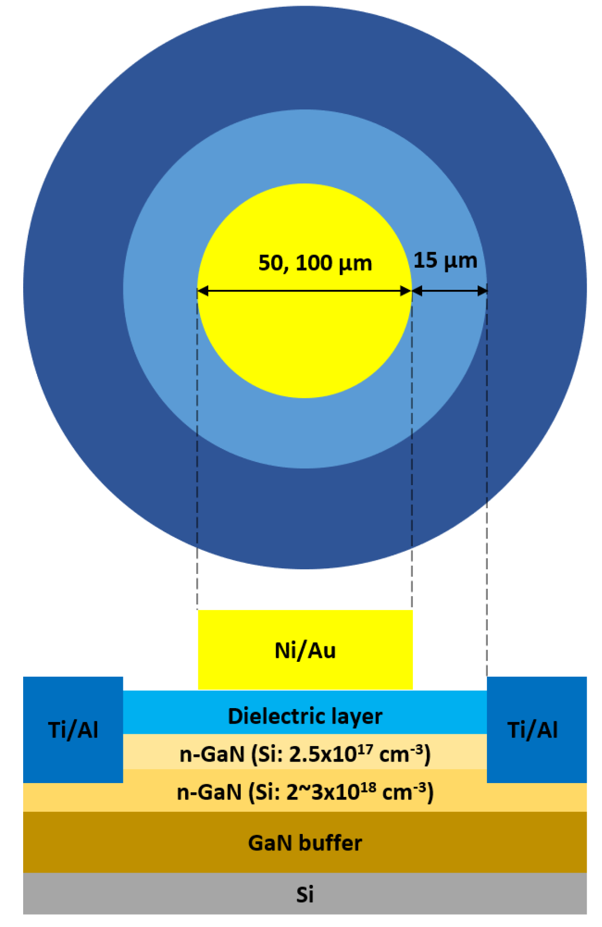
MIS capacitors using n-GaN wafers were fabricated to investigate the electrical properties of AlN on n-GaN. The epitaxial layers consisted of a 300 nm n-GaN layer with a Si doping concentration of 2.5 × 1017 cm−3, 700 nm n-type GaN layer, 700 nm n-GaN layer with a 2–3 × 1018 cm−3 Si doping concentration, and 3900 nm GaN buffer layer grown on an Si substrate. The effect of NH3 plasma power on the electrical characteristics of AlN was determined by fabricating MIS capacitors with different plasma powers of 30, 50, and 100 W. Ex situ and in situ treatments were conducted before the AlN deposition. The ex situ treatment included SPM and diluted HF (10:1) to remove organic contaminants and native oxides on the GaN surface. The in situ treatment included TMA pulsing (10 times with a duration of 0.2 s) and NH3 thermal treatment for 5 min; these two treatments were conducted to remove oxides and for surface nitridation, respectively. After AlN deposition, postdeposition annealing (PDA) was conducted at 500 °C for 10 min in an ambient N2 atmosphere. Following ohmic patterning and ohmic recess, ohmic contacts were formed with Ti/Al (40/200 nm) metallization. The ohmic contact formation was annealed at 500 °C under an ambient N2 atmosphere for 1 min. Finally, an Ni/Au (40/130 nm) metal electrode was deposited via e-gun evaporation. The circular metal electrodes had diameters of either 100 μm or 50 μm and were separated by a gap of 15 μm from a concentric contact, as shown in Figure 2.
XRD and XRR measurements were performed using a SmartLab diffractometer (Rigaku, Tokyo, Japan) to determine the crystallinity and mass density of the AlN film, respectively. The cross-sections at the AlN/GaN interface were examined using a STEM (JEM-2100F, JEOL). The chemical bonding states and components of AlN were determined via XPS (SIGMA PROBE, ThermoFisher Scientific, Waltham, MA, USA). Time-of-flight (TOF)-SIMS (TOF-SIMS.5, ION-TOF, Münster, Germany) analysis was also performed on the AlN film to investigate the presence of GaOx at the AlN/GaN interface.
The J–Eeff and C–V characteristics of AlN/AlON/AlHfON on GaN MIS capacitors were also investigated. An AlON/AlHfON layer was deposited onto the AlN layer to reduce the leakage current and increase the dielectric constant. AlON/AlHfON on GaN MIS capacitors were also fabricated as reference devices. The effective electric field was defined as (applied voltage–flat band voltage)/capacitance-equivalent thickness (CET). PEALD AlON, and AlHfON films were deposited using trimethylaluminum (TMA), tetrakis(dimethylamido)hafnium (TDMAHf), N2 plasma, and ozone as the Al, Hf, N, and O precursors, respectively. The substrate temperature and N2 plasma power were 330 °C and 30 W, respectively. The AlHfON film was deposited using the nanolaminate technique with alternating stacks of AlON and HfO2 films with an equal cycle ratio of 1:1.
3. Results
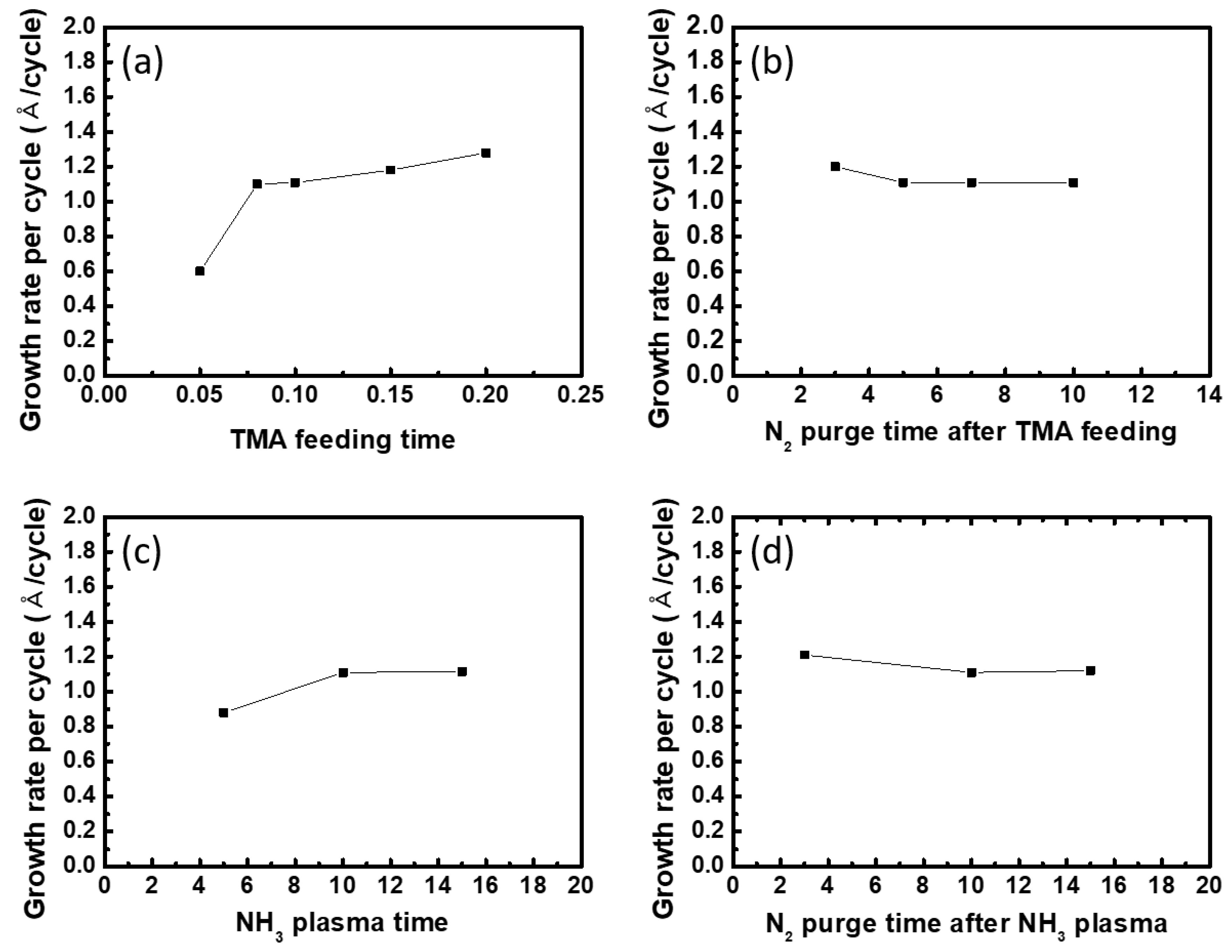
Figure 3 shows the growth rate per cycle (GPC) as a function of the process step time. The deposition temperature was 330 °C, and the NH3 plasma power was 100 W. The GPC was saturated at a TMA feeding time of 0.1 s and NH3 plasma time of 10 s, and the saturated value was 1.1 Å/cycle. The purge times after the TMA precursor injection and NH3 plasma step were chosen as 7 and 10 s, respectively.
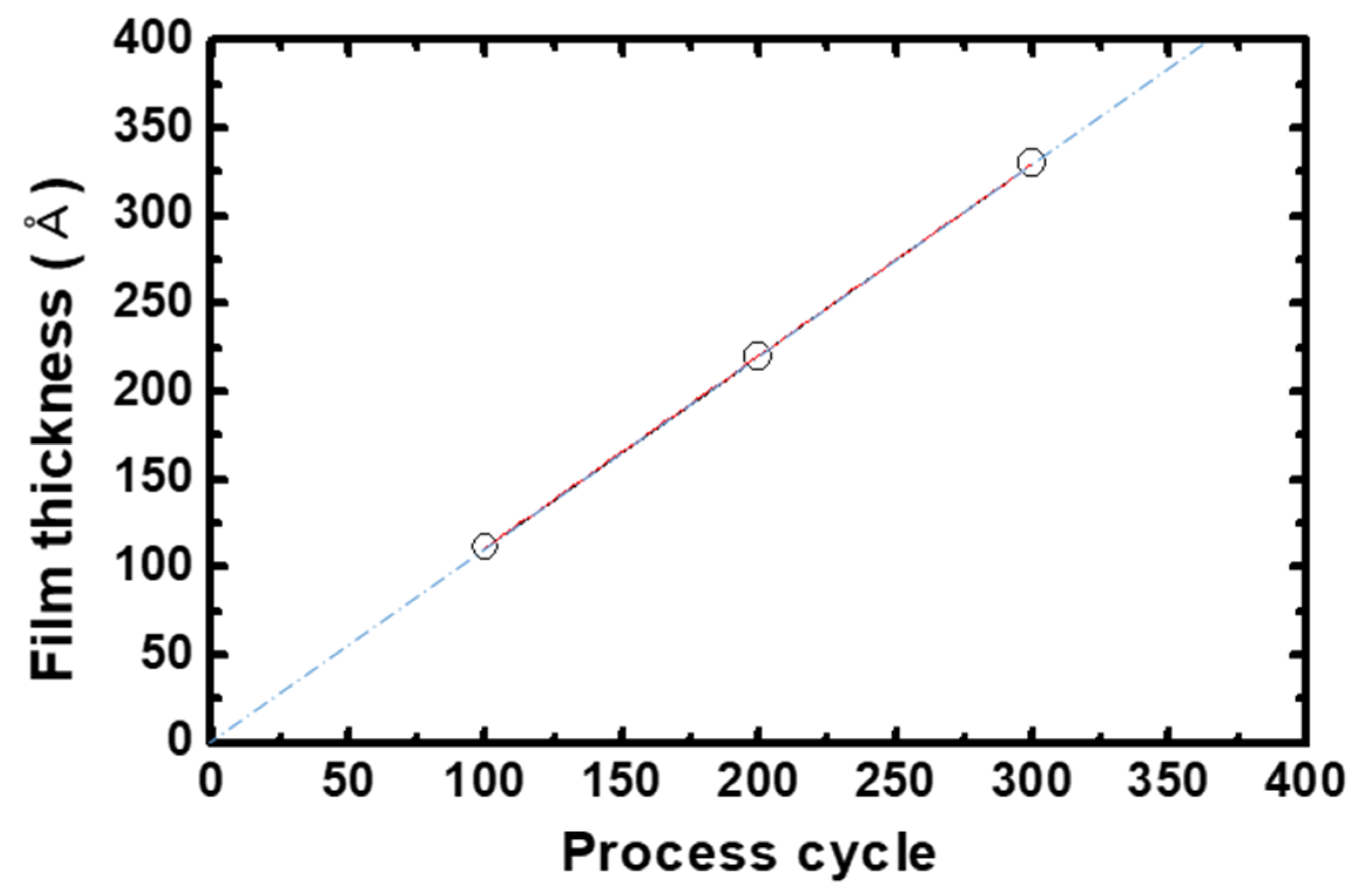
Figure 4 shows the linear dependence of the AlN film thickness, measured using ellipsometry, on the number of ALD cycles. The thickness increased linearly as the number of cycles increased without any incubation period. An interface layer was not observed between the Si and AlN, which can be attributed to the suppression of surface oxidation by AlN.
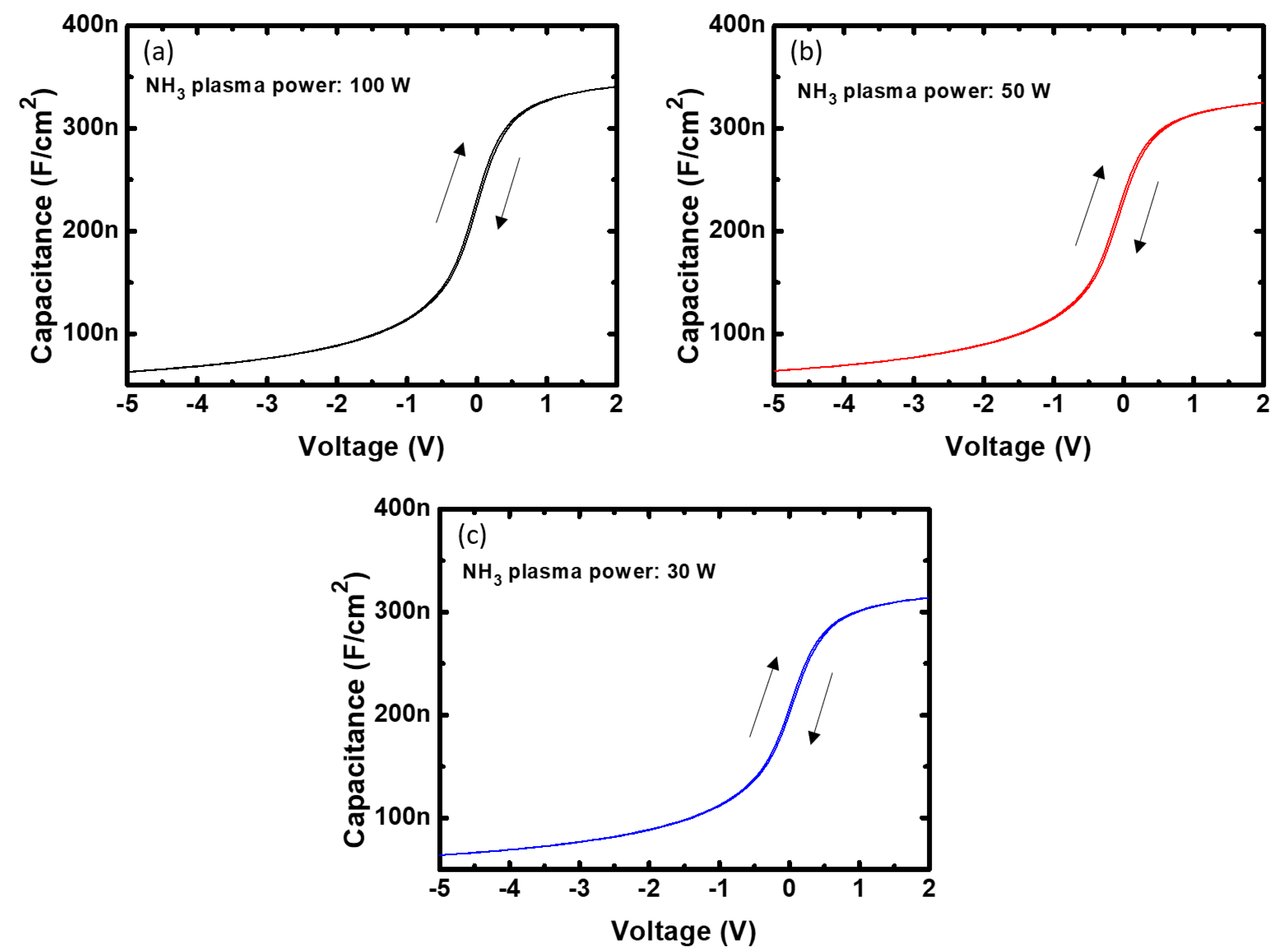
Figure 5 shows the double sweep C–V characteristics of AlN on n-GaN capacitors with various NH3 plasma powers when the bias was swept from −5 V to 2 V and back to −5 V. The C–V measurements were performed at 1 MHz. The C–V hysteresis characteristics of the MIS capacitors were almost identical regardless of the change in the NH3 plasma power, and exhibited minor hysteresis. The dielectric constants of the AlN films prepared using 30, 50, and 100 W NH3 plasma were 8.2, 7.8, and 8.1, respectively.
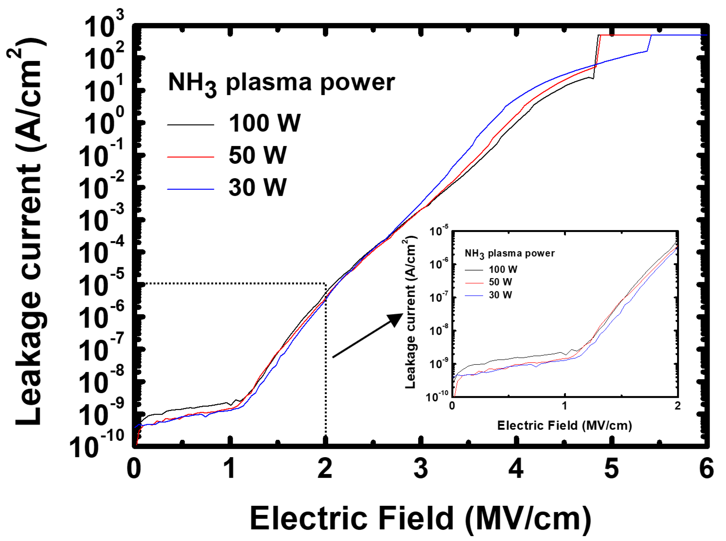
The J–E characteristics of AlN on the n-GaN capacitor with an NH3 plasma power of 30 W indicated a higher breakdown field and lower leakage current at a low electrical field compared to the other capacitors with plasma powers over 30 W, as shown in Figure 6. The low plasma power at the NH3 plasma step was considered to reduce the plasma-induced damage on the n-GaN surface, resulting in better J–V characteristics of the AlN on the n-GaN capacitor [28]. In conclusion, a TMA feeding time of 0.1 s, purge time of 7 s after the TMA precursor injection step, NH3 gas stabilization time of 3 s, NH3 plasma time of 10 s at 30 W, purge time of 10 s after the NH3 plasma step, and deposition temperature of 330 °C were chosen as the optimized deposition conditions for the fabrication of AlN on n-GaN.
To investigate the film quality, various characterization methods were conducted using films deposited under optimum conditions. Figure 7a shows the θ–2θ XRD patterns of a 100 nm-thick AlN layer deposited on n-GaN. Two diffraction peaks at 2θ values of ~33°, and ~36° were observed, which corresponded to the (100) and (002) planes, respectively [29,30]. The peak at ~31° is an artifact related to the high power of 9 kW. As shown in Figure 7b, the crystal quality was characterized using the rocking curve of AlN (002). The measured full width at half-maximum (FWHM) was 1050 arcsec, and the density of the ALD AlN which was evaluated by fitting the XRR data was 3.27 g/cm3, which is higher than the values reported in earlier studies [31,32]. These results indicate that highly crystalline AlN can be achieved at a low growth temperature of 330 °C.
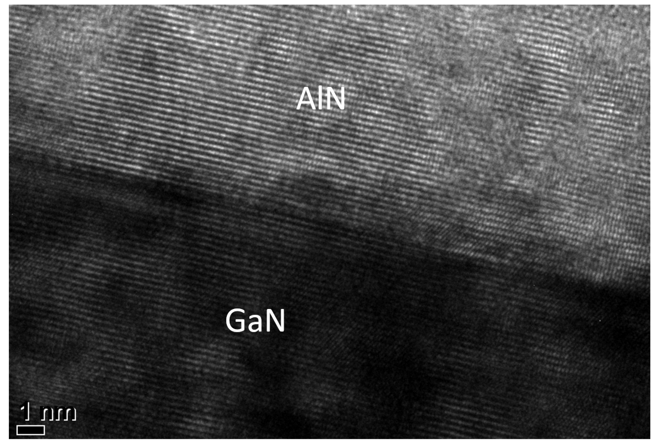
Figure 8 shows the STEM cross-sectional image of ~10 nm AlN on n-GaN. Crystalline AlN was observed in the image, and a sharp interface between the n-GaN and ALD AlN was confirmed, indicating the successful suppression of the surface oxidation of GaN by the introduction of an AlN layer.
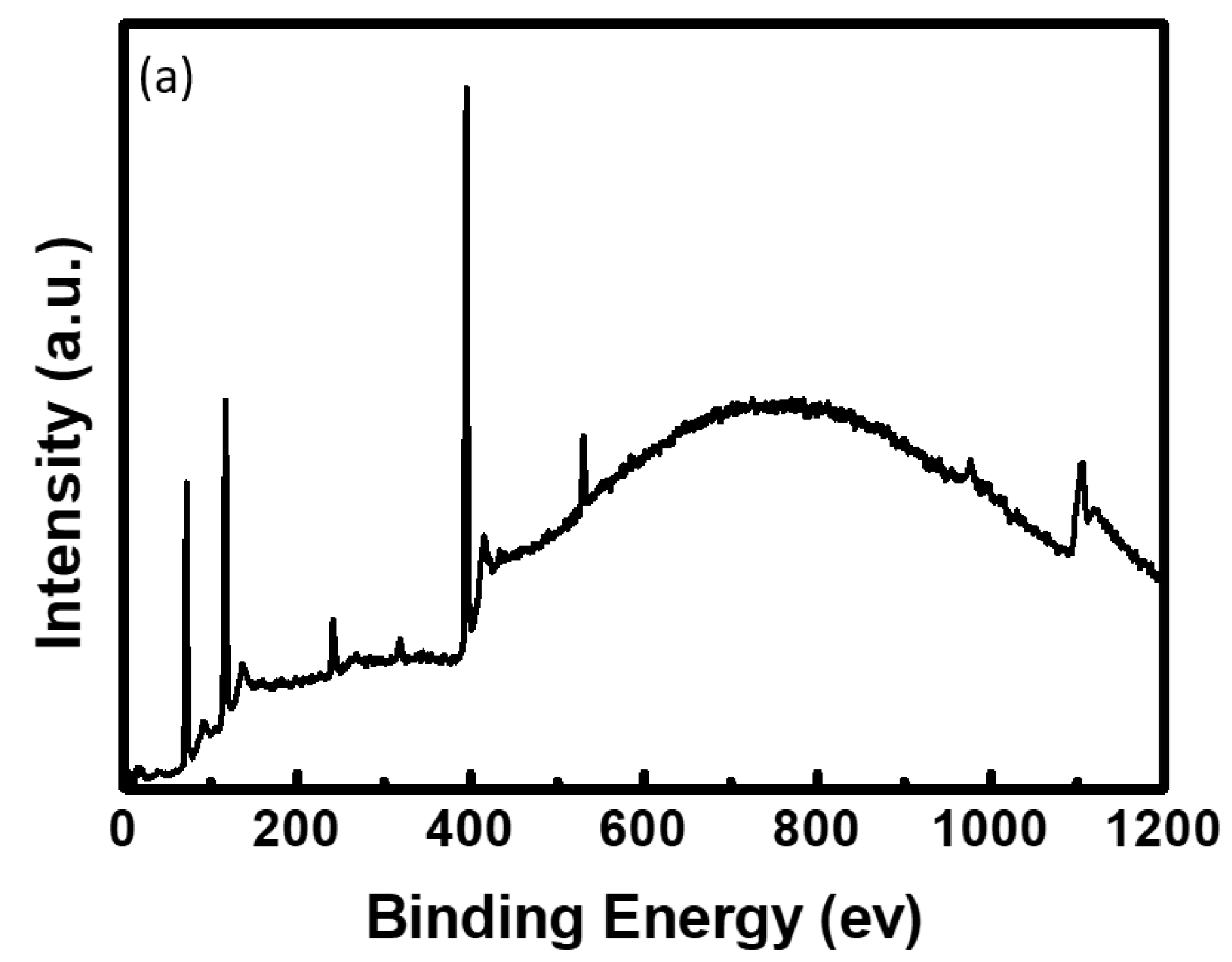
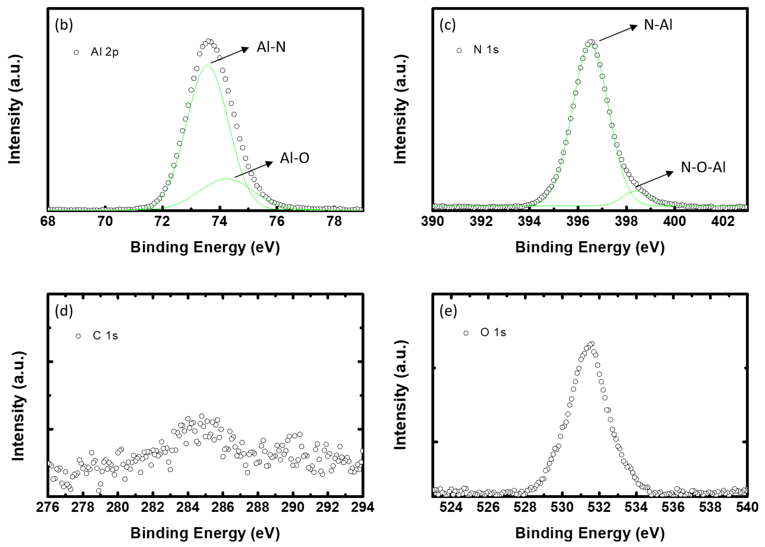
Figure 9 shows the XPS spectra of Al2p, N1s, C1s, and O1s of ~22 nm AlN on n-GaN. The deconvoluted Al2p spectra show two peaks at binding energies of 73.6 eV and 74.2 eV, which are associated with Al–N and Al–O bonds, respectively [33]. Binding energies of 396.5 eV and 398.4 eV were observed in the deconvoluted N1s spectra and are associated with N–Al and N–O–Al bonds, respectively [33]. The atomic concentrations of Al, N, C, and O in AlN were 47.4%, 44.2%, 0.9%, and 7.5%, respectively.
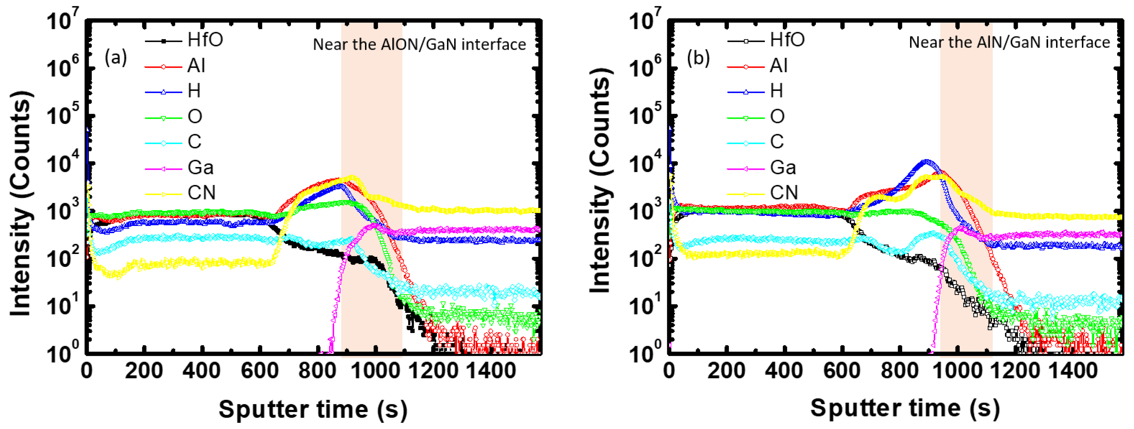
As previously discussed, the AlN layer showed low C–V hysteresis, confirming that it efficiently suppressed charge injection into the dielectrics. A low breakdown field of ~5 MV/cm and a high leakage current for an applied electric field of 2 MV/cm were also observed in the AlN MIS capacitors. An AlON/AlHfON layer was employed on the AlN layer to increase the breakdown field and reduce the leakage current of AlN. TOF-SIMS analysis of AlON/AlHfON and AlN/AlON/AlHfON on the n-GaN layer was conducted to obtain further information about the interface between AlN and n-GaN, and the results are shown in Figure 10. The oxygen intensity at the AlON/n-GaN interface was higher than that at the AlN/n-GaN interface, whereas the gallium intensity slope observed at the AlN/n-GaN interface was steeper than that observed at the AlON/n-GaN interface. These observations imply that using ALD AlN as an interfacial layer has an advantage compared to the use of AlON with O3 oxidant at the III–V interface because ALD AlN suppresses surface oxidation.
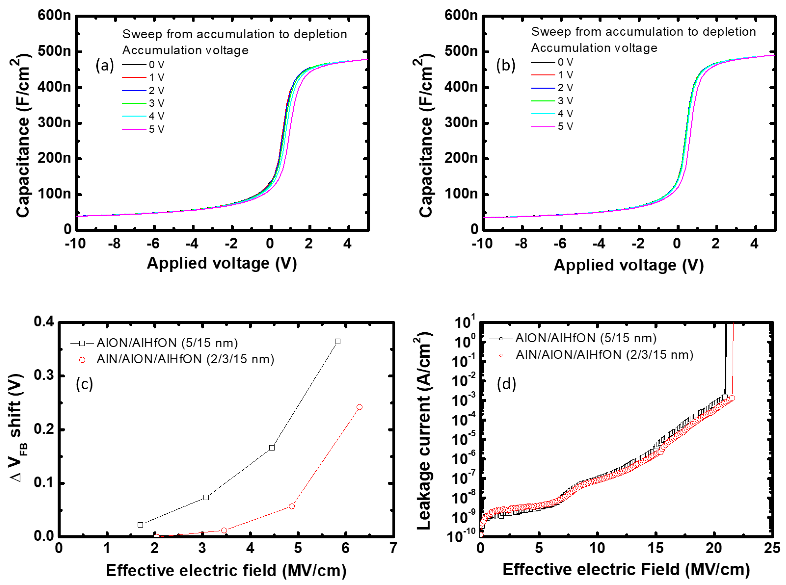
To evaluate the immunity against electron injection into the dielectrics, repeated C–V measurements were performed by sweeping the applied voltage from the accumulation to the depletion region [14]. The maximum accumulation voltage was increased in steps of 1 V by 5 V, and the depletion voltage was set to −10 V. The C–V characteristics of the MIS capacitors swept from the accumulation to depletion region, and the VFB shift of MIS capacitors as a function of the accumulation voltage are shown in Figure 11a–c. The MIS capacitor with AlN as an interfacial layer exhibited a smaller VFB shift compared to the MIS capacitor without the AlN interfacial layer. A VFB drift of 242 mV was observed for the MIS capacitor with AlN after sweeping from 5 V to −10 V, whereas a VFB drift of 365 mV was confirmed for the MIS capacitor without AlN. This difference indicates that there are fewer interface states between AlN and GaN than between AlON and GaN owing to the suppression of the formation of interfacial oxides. Figure 11d shows the J–Eeff characteristics of the fabricated MIS capacitors. Despite the high leakage current characteristics of AlN, the MIS capacitor with AlN as an interfacial layer exhibited leakage current characteristics similar to those of MIS capacitors without AlN.
4. Conclusions
An AlN interfacial layer using TMA and NH3 plasma in a PEALD system was developed to improve the dielectric/GaN interface characteristics. The optimized AlN process conditions were as follows: TMA feeding for 0.1 s, N2 purge for 7 s after TMA feeding, NH3 gas stabilization for 3 s, NH3 plasma for 10 s at 30 W, N2 purge for 10 s after NH3 plasma, and a deposition temperature of 330 °C. The PEALD process ensured a high linearity between the AlN thickness and the number of cycles. Two different diffraction peaks at 2θ values of ~33° and ~36° corresponding to (100) and (002) planes, respectively, were observed in the XRD measurements, and the density of the ALD AlN was 3.27 g/cm3 from the XRR measurement. The AlN interfacial layer successfully suppressed the GaN surface oxidation and improved the VFB drift characteristics of the MIS capacitor, showing excellent leakage current characteristics. Thus, it is suggested that the low-temperature PEALD AlN is a promising interfacial layer with a high crystal quality for GaN.
Author Contributions
Process set-up: I.-H.H. and M.-J.K.; investigation: I.-H.H. and M.-J.K.; formal analysis: I.-H.H.; conceptualization: I.-H.H., H.-Y.C., and K.-S.S.; methodology: I.-H.H., H.-Y.C., and K.-S.S.; visualization: I.-H.H.; writing—original draft preparation: I.-H.H., H.-Y.C., and K.-S.S.; writing—review and editing: I.-H.H., H.-Y.C., and K.-S.S.; supervision: H.-Y.C. and K.-S.S. All authors have read and agreed to the published version of the manuscript.
Funding
This work was supported by the Ministry of Trade, Industry & Energy (10067636) and the Basic Science Research Program (No. 2015R1A6A1A03031833 and No. 2019R1A2C1008894).
Acknowledgments
Myoung-Jin Kang currently works at the future technology R&D center, SK Hynix Co., Ltd., KOREA.
Conflicts of Interest
The authors declare no conflict of interest.
References
- Lu, Y.; Yang, S.; Jiang, Q.; Tang, Z.; Li, B.; Chen, K.J. Characterization of VT-instability in enhancement-mode Al2O3-AlGaN/GaN MIS-HEMTs. Phys. Status Solidi Curr. Top. Solid State Phys. 2013, 10, 1397–1400. [Google Scholar] [CrossRef]
- Lagger, P.; Ostermaier, C.; Pobegen, G.; Pogany, D. Towards understanding the origin of threshold voltage instability of AlGaN/GaN MIS-HEMTs. Tech. Dig. Int. Electron Devices Meet. IEDM 2012, 299–302. [Google Scholar] [CrossRef]
- He, J.; Hua, M.; Zhang, Z.; Chen, K.J. Performance and VTH Stability in E-Mode GaN Fully Recessed MIS-FETs and Partially Recessed MIS-HEMTs with LPCVD-SiNx/PECVD-SiNx Gate Dielectric Stack. IEEE Trans. Electron Devices 2018, 65, 3185–3191. [Google Scholar] [CrossRef]
- Wada, Y.; Nozaki, M.; Hosoi, T.; Shimura, T.; Watanabe, H. Insight into gate dielectric reliability and stability of SiO2/GaN MOS devices. Jpn. J. Appl. Phys. 2020, 59. [Google Scholar] [CrossRef]
- Lee, J.G.; Kim, H.S.; Seo, K.S.; Cho, C.H.; Cha, H.Y. High quality PECVD SiO2 process for recessed MOS-gate of AlGaN/GaN-on-Si metal-oxide-semiconductor heterostructure field-effect transistors. Solid State Electron. 2016, 122, 32–36. [Google Scholar] [CrossRef]
- Hu, Q.; Li, S.; Li, T.; Wang, X.; Li, X.; Wu, Y. Channel engineering of normally-OFF AlGaN/GaN MOS-HEMTs by atomic layer etching and high-κDielectric. IEEE Electron Device Lett. 2018, 39, 1377–1380. [Google Scholar] [CrossRef]
- Maeda, E.; Nabatame, T.; Yuge, K.; Hirose, M.; Inoue, M.; Ohi, A.; Ikeda, N.; Shiozaki, K.; Kiyono, H. Change of characteristics of n-GaN MOS capacitors with Hf-rich HfSiOx gate dielectrics by post-deposition annealing. Microelectron. Eng. 2019, 216, 111036. [Google Scholar] [CrossRef]
- Hwang, I.H.; Eom, S.K.; Choi, G.H.; Kang, M.J.; Lee, J.G.; Cha, H.Y.; Seo, K.S. High-Performance E-Mode AlGaN/GaN MIS-HEMT with Dual Gate Insulator Employing SiON and HfON. Phys. Status Solidi Appl. Mater. Sci. 2018, 215, 1–6. [Google Scholar] [CrossRef]
- Kim, H.S.; Han, S.W.; Jang, W.H.; Cho, C.H.; Seo, K.S.; Oh, J.; Cha, H.Y. Normally-Off GaN-on-Si MISFET Using PECVD SiON Gate Dielectric. IEEE Electron Device Lett. 2017, 38, 1090–1093. [Google Scholar] [CrossRef]
- Jiang, H.; Tang, C.W.; Lau, K.M. Enhancement-Mode GaN MOS-HEMTs with Recess-Free Barrier Engineering and High-k ZrO2 Gate Dielectric. IEEE Electron Device Lett. 2018, 39, 405–408. [Google Scholar] [CrossRef]
- Anderson, T.J.; Wheeler, V.D.; Shahin, D.I.; Tadjer, M.J.; Koehler, A.D.; Hobart, K.D.; Christou, A.; Kub, F.J.; Eddy, C.R. Enhancement mode AlGaN/GaN MOS high-electron-mobility transistors with ZrO2 gate dielectric deposited by atomic layer deposition. Appl. Phys. Express 2016, 9, 071003. [Google Scholar] [CrossRef]
- Uenuma, M.; Takahashi, K.; Sonehara, S.; Tominaga, Y.; Fujimoto, Y.; Ishikawa, Y.; Uenuma, M.; Takahashi, K.; Sonehara, S.; Tominaga, Y. Influence of carbon impurities and oxygen vacancies in Al2O3 film on Al2O3/GaN MOS capacitor characteristics Influence of carbon impurities and oxygen vacancies in Al2O3 film on Al2O3/GaN MOS capacitor characteristics. AIP Adv. 2018, 105103. [Google Scholar] [CrossRef] [Green Version]
- Zhu, J.; Hou, B.; Chen, L.; Zhu, Q.; Yang, L.; Zhou, X.; Zhang, P.; Ma, X.; Hao, Y. Threshold Voltage Shift and Interface/Border Trapping Mechanism in Al2O3/AlGaN/GaN MOS-HEMTs. In Proceedings of the 2018 IEEE International Reliability Physics Symposium (IRPS), Burlingame, CA, USA, 11–15 March 2018; pp. 8–11. [Google Scholar] [CrossRef]
- Nozaki, M.; Watanabe, K.; Yamada, T.; Shih, H.A.; Nakazawa, S.; Anda, Y.; Ueda, T.; Yoshigoe, A.; Hosoi, T.; Shimura, T.; et al. Implementation of atomic layer deposition-based AlON gate dielectrics in AlGaN/GaN MOS structure and its physical and electrical properties. Jpn. J. Appl. Phys. 2018, 57, 06KA02. [Google Scholar] [CrossRef] [Green Version]
- Kang, M.J.; Eom, S.K.; Kim, H.S.; Lee, C.H.; Cha, H.Y.; Seo, K.S. Normally-off recessed-gate AlGaN/GaN MOS-HFETs with plasma enhanced atomic layer deposited AlOxNy gate insulator. Semicond. Sci. Technol. 2019, 34. [Google Scholar] [CrossRef]
- Liu, C.; Chor, E.F.; Tan, L.S. Enhanced device performance of AlGaN/GaN HEMTs using HfO2 high-k dielectric for surface passivation and gate oxide. Semicond. Sci. Technol. 2007, 22, 522–527. [Google Scholar] [CrossRef]
- Chang, Y.C.; Huang, M.L.; Chang, Y.H.; Lee, Y.J.; Chiu, H.C.; Kwo, J.; Hong, M. Atomic-layer-deposited Al2O3 and HfO2 on GaN: A comparative study on interfaces and electrical characteristics. Microelectron. Eng. 2011, 88, 1207–1210. [Google Scholar] [CrossRef]
- Ozaki, S.; Ohki, T.; Kanamura, M.; Imada, T.; Nakamura, N.; Okamoto, N.; Miyajima, T.; Kikkawa, T. Effect of oxidant source on threshold voltage shift of AlGaN/GaN MIS-HEMTs using ALD-Al2O3 gate insulator films. In Proceedings of the 2012 CS MANTECH Conference, Boston, MA, USA, 23–26 April 2012; pp. 3–6. [Google Scholar]
- Yang, S.; Tang, Z.; Wong, K.; Lin, Y.; Liu, C.; Lu, Y.; Huang, S.; Chen, K.J. High-Quality Interface in Al2O3/GaN/GaNAlGaNGaN MIS Structures with in Situ Pre-Gate Plasma Nitridation. IEEE Electron Device Lett. 2013, 34, 1497–1499. [Google Scholar] [CrossRef]
- Shen, Z.; He, L.; Zhou, G.; Yao, Y.; Yang, F.; Ni, Y.; Zheng, Y.; Zhou, D.; Ao, J.; Zhang, B.; et al. Investigation of O3-Al2O3/H2O-Al2O3 dielectric bilayer deposited by atomic-layer deposition for GaN MOS capacitors. Phys. Status Solidi Appl. Mater. Sci. 2016, 213, 2693–2698. [Google Scholar] [CrossRef]
- Eom, S.K.; Kong, M.W.; Kang, M.J.; Lee, J.G.; Cha, H.Y.; Seo, K.S. Enhanced Interface Characteristics of PA-ALD HfOxNy/InGaAs MOSCAPs Using IPA Oxygen Reactant and Cyclic N2 Plasma. IEEE Electron Device Lett. 2018, 39, 1636–1639. [Google Scholar] [CrossRef]
- Huang, S.; Jiang, Q.; Yang, S.; Zhou, C.; Chen, K.J. Effective passivation of AlGaN/GaN HEMTs by ALD-grown AlN thin film. IEEE Electron Device Lett. 2012, 33, 516–518. [Google Scholar] [CrossRef]
- Hsieh, T.E.; Chang, E.Y.; Song, Y.Z.; Lin, Y.C.; Wang, H.C.; Liu, S.C.; Salahuddin, S.; Hu, C.C. Gate recessed quasi-normally off Al2O3/AlGaN/GaN MIS-HEMT with low threshold voltage hysteresis using PEALD AlN interfacial passivation layer. IEEE Electron Device Lett. 2014, 35, 732–734. [Google Scholar] [CrossRef]
- Kim, H.; Kim, N.D.; An, S.C.; Yoon, H.J.; Choi, B.J. Improved interfacial properties of thermal atomic layer deposited AlN on GaN. Vacuum 2019, 159, 379–381. [Google Scholar] [CrossRef]
- Tarala, V.A.; Altakhov, A.S.; Martens, V.Y.; Lisitsyn, S.V. Growing aluminum nitride films by Plasma-Enhanced Atomic Layer Deposition at low temperatures. In Journal of Physics: Conference Series; IOP Publishing: Bristol, UK, 2015; p. 652. [Google Scholar] [CrossRef]
- Dallaeva, D.S.; Bilalov, B.A.; Gitikchiev, M.A.; Kardashova, G.D.; Safaraliev, G.K.; Tománek, P.; Škarvada, P.; Smith, S. Structural properties of Al2O3/AlN thin film prepared by magnetron sputtering of Al in HF-activated nitrogen plasma. Thin Solid Films 2012, 526, 92–96. [Google Scholar] [CrossRef]
- Dallaev, R.; Sobola, D.; Tofel, P.; Škvarenina, L.; Sedlák, P. Aluminum nitride nanofilms by atomic layer deposition using alternative precursors hydrazinium chloride and triisobutylaluminum. Coatings 2020, 10, 954. [Google Scholar] [CrossRef]
- Knoops, H.C.M.; Faraz, T.; Arts, K.; Kessels, W.M.M. (Erwin) Status and prospects of plasma-assisted atomic layer deposition. J. Vac. Sci. Technol. A 2019, 37, 030902. [Google Scholar] [CrossRef] [Green Version]
- Shih, H.Y.; Lee, W.H.; Kao, W.C.; Chuang, Y.C.; Lin, R.M.; Lin, H.C.; Shiojiri, M.; Chen, M.J. Low-temperature atomic layer epitaxy of AlN ultrathin films by layer-by-layer, in-situ atomic layer annealing. Sci. Rep. 2017, 7, 1–8. [Google Scholar] [CrossRef] [Green Version]
- Zhu, Z.; Ostreng, E.; Tuoriniemi, I.; Chen, Z.; Niiranen, K.; Sneck, S. Batch atomic layer deposition of aluminum nitride for RF-MEMS and GAN power-devices. In Proceedings of the 2019 China Semiconductor Technology International Conference (CSTIC), Shangai, China, 18–19 March 2019; pp. 1–3. [Google Scholar] [CrossRef]
- Abdulagatov, A.I.; Ramazanov, S.M.; Dallaev, R.S.; Murliev, E.K.; Palchaev, D.K.; Rabadanov, M.K.; Abdulagatov, I.M. Atomic Layer Deposition of Aluminum Nitride Using Tris(diethylamido)aluminum and Hydrazine or Ammonia. Russ. Microelectron. 2018, 47, 118–130. [Google Scholar] [CrossRef]
- Alevli, M.; Ozgit, C.; Donmez, I.; Biyikli, N. Structural properties of AlN films deposited by plasma-enhanced atomic layer deposition at different growth temperatures. Phys. Status Solidi Appl. Mater. Sci. 2012, 209, 266–271. [Google Scholar] [CrossRef]
- Cao, D.; Cheng, X.; Xie, Y.H.; Zheng, L.; Wang, Z.; Yu, X.; Wang, J.; Shen, D.; Yu, Y. Effects of rapid thermal annealing on the properties of AlN films deposited by PEALD on AlGaN/GaN heterostructures. RSC Adv. 2015, 5, 37881–37886. [Google Scholar] [CrossRef] [Green Version]
Figure 1.
Schematic of plasma-enhanced atomic layer deposition (PEALD) system used for the experiments.
Figure 1.
Schematic of plasma-enhanced atomic layer deposition (PEALD) system used for the experiments.

Figure 2.
Cross-sectional schematic of the fabricated metal-insulator-semiconductor (MIS) capacitors.
Figure 2.
Cross-sectional schematic of the fabricated metal-insulator-semiconductor (MIS) capacitors.

Figure 3.
(a–d) Growth rate per cycle (GPC) values for AlN deposited using the PEALD system as a function of the trimethylaluminum (TMA) feeding time, N2 purge time after TMA feeding, NH3 plasma time, and N2 purge time after NH3 plasma (NH3 plasma power: 100 W).
Figure 3.
(a–d) Growth rate per cycle (GPC) values for AlN deposited using the PEALD system as a function of the trimethylaluminum (TMA) feeding time, N2 purge time after TMA feeding, NH3 plasma time, and N2 purge time after NH3 plasma (NH3 plasma power: 100 W).

Figure 4.
AlN film thickness values as a function of ALD cycles (NH3 plasma power: 100 W).

Figure 5.
C–V characteristics of the AlN metal-insulator-semiconductor (MIS) capacitors. NH3 plasma power (AlN thickness): (a) 100 W (20.8 nm), (b) 50 W (21.3 nm), and (c) 30 W (22.9 nm).
Figure 5.
C–V characteristics of the AlN metal-insulator-semiconductor (MIS) capacitors. NH3 plasma power (AlN thickness): (a) 100 W (20.8 nm), (b) 50 W (21.3 nm), and (c) 30 W (22.9 nm).

Figure 6.
J–E characteristics of the MIS capacitors.

Figure 7.
(a) XRD result and (b) rocking curve of (002) of the ALD AlN of ~100 nm on n-GaN and (c) XRR result of the ALD AlN of ~30 nm on n-GaN (NH3 plasma power: 30 W).
Figure 7.
(a) XRD result and (b) rocking curve of (002) of the ALD AlN of ~100 nm on n-GaN and (c) XRR result of the ALD AlN of ~30 nm on n-GaN (NH3 plasma power: 30 W).

Figure 8.
Cross-sectional STEM image of the AlN/n-GaN interface (NH3 plasma power: 30 W).

Figure 9.
(a) Wide-scan XPS spectra and high-resolution XPS spectra of the (b) Al 2p, (c) N 1s, (d) C 1s, and (e) O 1s of the ALD AlN (NH3 plasma power: 30 W).
Figure 9.
(a) Wide-scan XPS spectra and high-resolution XPS spectra of the (b) Al 2p, (c) N 1s, (d) C 1s, and (e) O 1s of the ALD AlN (NH3 plasma power: 30 W).


Figure 10.
Time-of-flight (TOF)-secondary ion mass spectrometry (SIMS) results for (a) AlON/AlHfON (~5/~15 nm) and (b) AlN/AlON/AlHfON (~2/~3/~15 nm) on n-GaN (NH3 plasma power: 30 W).
Figure 10.
Time-of-flight (TOF)-secondary ion mass spectrometry (SIMS) results for (a) AlON/AlHfON (~5/~15 nm) and (b) AlN/AlON/AlHfON (~2/~3/~15 nm) on n-GaN (NH3 plasma power: 30 W).

Figure 11.
(a,b) C–V characteristics of the GaN MIS capacitors with accumulation voltages ranging from 0 V to 5 V; (c) VFB shift as a function of the effective electric field in the fabricated GaN MIS capacitors; and (d) J–Eeff characteristics of the fabricated MIS capacitors (NH3 plasma power: 30 W).

Publisher’s Note: MDPI stays neutral with regard to jurisdictional claims in published maps and institutional affiliations. |
© 2021 by the authors. Licensee MDPI, Basel, Switzerland. This article is an open access article distributed under the terms and conditions of the Creative Commons Attribution (CC BY) license (https://creativecommons.org/licenses/by/4.0/).
Share and Cite
MDPI and ACS Style
Hwang, I.-H.; Kang, M.-J.; Cha, H.-Y.; Seo, K.-S. Crystalline AlN Interfacial Layer on GaN Using Plasma-Enhanced Atomic Layer Deposition. Crystals 2021, 11, 405. https://0-doi-org.brum.beds.ac.uk/10.3390/cryst11040405
AMA Style
Hwang I-H, Kang M-J, Cha H-Y, Seo K-S. Crystalline AlN Interfacial Layer on GaN Using Plasma-Enhanced Atomic Layer Deposition. Crystals. 2021; 11(4):405. https://0-doi-org.brum.beds.ac.uk/10.3390/cryst11040405
Chicago/Turabian StyleHwang, Il-Hwan, Myoung-Jin Kang, Ho-Young Cha, and Kwang-Seok Seo. 2021. "Crystalline AlN Interfacial Layer on GaN Using Plasma-Enhanced Atomic Layer Deposition" Crystals 11, no. 4: 405. https://0-doi-org.brum.beds.ac.uk/10.3390/cryst11040405
Note that from the first issue of 2016, this journal uses article numbers instead of page numbers. See further details here.