
Deep-Level Traps Responsible for Persistent Photocurrent in Pulsed-Laser-Deposited β-Ga2O3 Thin Films


1
Department of Physics, Indian Institute of Technology, Delhi 110016, India
2
Department of Physics, University of Warwick, Coventry CV4 7AL, UK
*
Authors to whom correspondence should be addressed.
Crystals 2021, 11(9), 1046; https://0-doi-org.brum.beds.ac.uk/10.3390/cryst11091046
Submission received: 5 August 2021
/
Revised: 23 August 2021
/
Accepted: 23 August 2021
/
Published: 30 August 2021
(This article belongs to the Special Issue Wide Bandgap Semiconductor Materials and Devices)
Abstract
:Gallium oxide (β-Ga2O3) is emerging as a promising wide-bandgap semiconductor for optoelectronic and high-power electronic devices. In this study, deep-level defects were investigated in pulsed-laser-deposited epitaxial films of β-Ga2O3. A deep ultraviolet photodetector (DUV) fabricated on β-Ga2O3 film showed a slow decay time of 1.58 s after switching off 250 nm wavelength illumination. Generally, β-Ga2O3 possesses various intentional and unintentional trap levels. Herein, these traps were investigated using the fractional emptying thermally stimulated current (TSC) method in the temperature range of 85 to 473 K. Broad peaks in the net TSC curve were observed and further resolved to identify the characteristic peak temperature of individual traps using the fractional emptying method. Several deep-level traps having activation energies in the range of 0.16 to 1.03 eV were identified. Among them, the trap with activation energy of 1.03 eV was found to be the most dominant trap level and it was possibly responsible for the persistent photocurrent in PLD-grown β-Ga2O3 thin films. The findings of this current work could pave the way for fabrication of high-performance DUV photodetectors.
1. Introduction
The growing demand for high-performance power electronic devices is seeing an enormous thrust for advanced wide-bandgap semiconductor materials such as GaN, Ga2O3, and SiC. Ga2O3 has received huge attention from the scientific community owing to its material properties such as an ultra-wide bandgap, an extremely high Baliga’s figure of merit, and a large breakdown field [1,2,3,4,5]. The crystallization of Ga2O3 material has been reported in α, β, γ, ε, δ, and κ phases [6,7]. Among them, the β-phase of Ga2O3 has shown superiority due to the availability of melt-growth single crystals, and stability against radiation and thermal and chemical environments [8,9,10,11,12,13,14,15].
Being a wide-bandgap material, various intentional, as well as unintentional, trap levels in β-Ga2O3 have been reported. Therefore, investigation of electrically active defects is necessary pursuant to the excellent future of β-Ga2O3-based power electronics and optoelectronics. Previously, different defect levels in β-Ga2O3 single crystals, as well as thin films, have been studied using deep-level transient spectroscopy (DLTS), deep-level optical spectroscopy (DLOS), admittance spectroscopy, thermally stimulated current (TSC) spectroscopy, and thermally stimulated depolarization current (TSDC) spectroscopy [16,17,18]. An unintentional donor of 110 meV energy was identified in edge-defined film-fed grown (EFG) β-Ga2O3 single crystal [17]. Either native interstitial, or Si substitution at the octahedral Ga site, was proposed as the origin of this donor level. Tadjer et al. reported a trap located 0.23 eV below the conduction band in halide vapor phase epitaxial β-Ga2O3 which was co-doped by Si and N impurities [19]. The effect of twin boundaries that induced structural disorder on the electronic properties of homoepitaxial β-Ga2O3 thin films was also studied. It was identified, using DLTS, that an acceptor of 0.34 eV energy originating from twin lamellae was responsible for electrical compensation [20]. Iron (Fe) was the most common unintentional defect in β-Ga2O3 thin films as well as single-crystal substrates irrespective of the growth method. The Fe trap level of about 0.78 eV energy also behaved as an electrical compensator [16,21]. Zimmermann et al. also reported traps with activation energies of 0.66 and 0.73 eV in single-crystal substrates using the DLTS technique [22]. These energy levels were tentatively assigned for Fe substituting Ga at tetrahedral and octahedral positions, respectively. Titanium (Ti) is another possible deep-level defect with activation energy of 0.95 eV, which originates due to octahedral Ga substitution [22]. Irmscher et al. proposed that Co impurity may be responsible for trap levels at 0.55 and 1.04 eV [23]. Deep levels have been studied by Zhang et al. in the single crystal using both the DLTS and DLOS methods [16]. They observed traps at Ec −0.62 eV, 0.82 eV, 1.0 eV, 2.16 eV, and 4.40 eV below the conduction band. Wang et al. investigated the traps in β-Ga2O3 thin films using TSC and TSDC [18]. The films used for the measurements were grown in oxygen, argon, and a mixture of both gases. It was found that the thin films grown in an argon atmosphere possessed reduced traps compared to other growth conditions. However, they fitted the measured overlapped broad peaks. In this study, the TSC technique with fractional emptying method was adopted to investigate the traps in thin films. The fractional emptying method is advantageous over normal TSC for resolving overlapped traps.
In TSC spectroscopy, electrons and holes are filled via optical injection at a relatively lower temperature. Thereafter, these traps release carriers by constant temperature increment, which results in a characteristic peak related to the activation energy of the trap.
TSC Mechanism
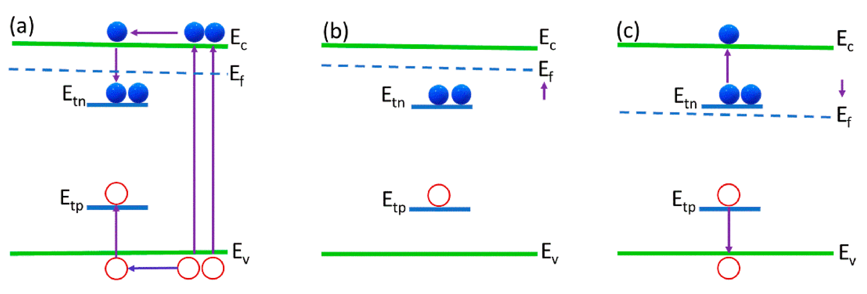
The mechanism of the TSC method can be explained using an energy band diagram as depicted in Figure 1a–c. When the material is excited with a light of energy hν, electrons excite from the valence band to the conduction band, which leads to splitting of the Fermi level (Ef) into electrons (Efn) and holes (Efp) quasi-Fermi levels. Consequently, an electron-hole equilibrium condition is established soon after the illumination [24]. Any perturbation from the equilibrium condition triggers the recombination process to achieve the electron-hole equilibrium condition [25]. The recombination may occur via electron capture, hole capture, electron emission from donors, or hole emission from acceptors. Figure 1a displays the equilibrium condition under optical illumination, which resulted in the complete trap filling. Figure 1b shows the band diagram after the complete trapping of electrons and holes. Both quasi-Fermi levels also moved towards their respective conduction band and valence band after equilibrium. In TSC, these trapped charge carriers were released by thermal energy. Therefore, a continuous rise in the stimulated current appeared as the probability of the carrier emptying increased. The band diagram under the thermal release of carriers is shown in Figure 1c. Further, the current started to decrease after the thermal release of electrons/holes from a particular trap that resulted in a TSC peak. With the continuous increase in temperature, more deeper traps started to release the charge carriers, and both quasi-Fermi levels reached the intrinsic position after complete emptying.
In the variable heating method of TSC, the activation energy (ET) of a trap state at a heating rate of can be approximated as [18]:
where Tm is the characteristic temperature of the TSC peak.
2. Experimental
β-Ga2O3 thin films fabricated on c-plane sapphire substrates were used for device fabrication. The thin films were grown at 800 °C substrate temperature and 0.5 mTorr oxygen partial pressure. The growth was uniformly conducted on a 10 × 10 mm2 substrate. The Ga2O3 target was ablated using a KrF excimer laser which had a 248 nm excitation wavelength. Laser fluence and repetition were 1.4 J/cm2 and 10 Hz, respectively. Other details about the thin film growth can be found in our previous reports [14]. MSM-interdigitated electrode structures were used for TSC measurements. These electrode structures were patterned in a Class 100 clean room environment with the help of an optical lithography system (Intelligent micropatterning, SF-100). After patterning, Ni (30 nm) and Au (60 nm) were thermally evaporated, and the desired device structure was acquired by a metal lift-off process. The length, width, and finger spacing of electrodes were 700, 50, and 50 μm, respectively. Further, the device was probed in an optical cryostat (Janis VPF-700, Coventry, UK) equipped with a temperature controller. The material needed to be stimulated using an appropriate wavelength of light, which was 250 nm (50 µW/cm2) in this case. The optical injection should be performed at a low enough temperature to prevent the release of trapped charge carriers by thermal energy. Therefore, the device was cooled down to a lowest temperature of 83 K under dark conditions. The temperature was chosen by considering the large range of trap levels in the wide bandgap of β-Ga2O3. Here, the temperature selection was also limited by the cryogenic system, which was governed by liquid nitrogen. To establish maximum trap filling, uniform illumination of the device was performed until the photocurrent became saturated. No external voltage bias was applied to the device during the measurements. Thereafter, the optical injection was turned off, and the device was heated up with a constant heating rate of 7 K/min with zero external bias. The maximum heating temperature was set as 473 K, and then the device was cooled down. The current was simultaneously recorded with a high-impedance source meter (Keithley, 6517, Delhi, India).
3. Results and Discussion
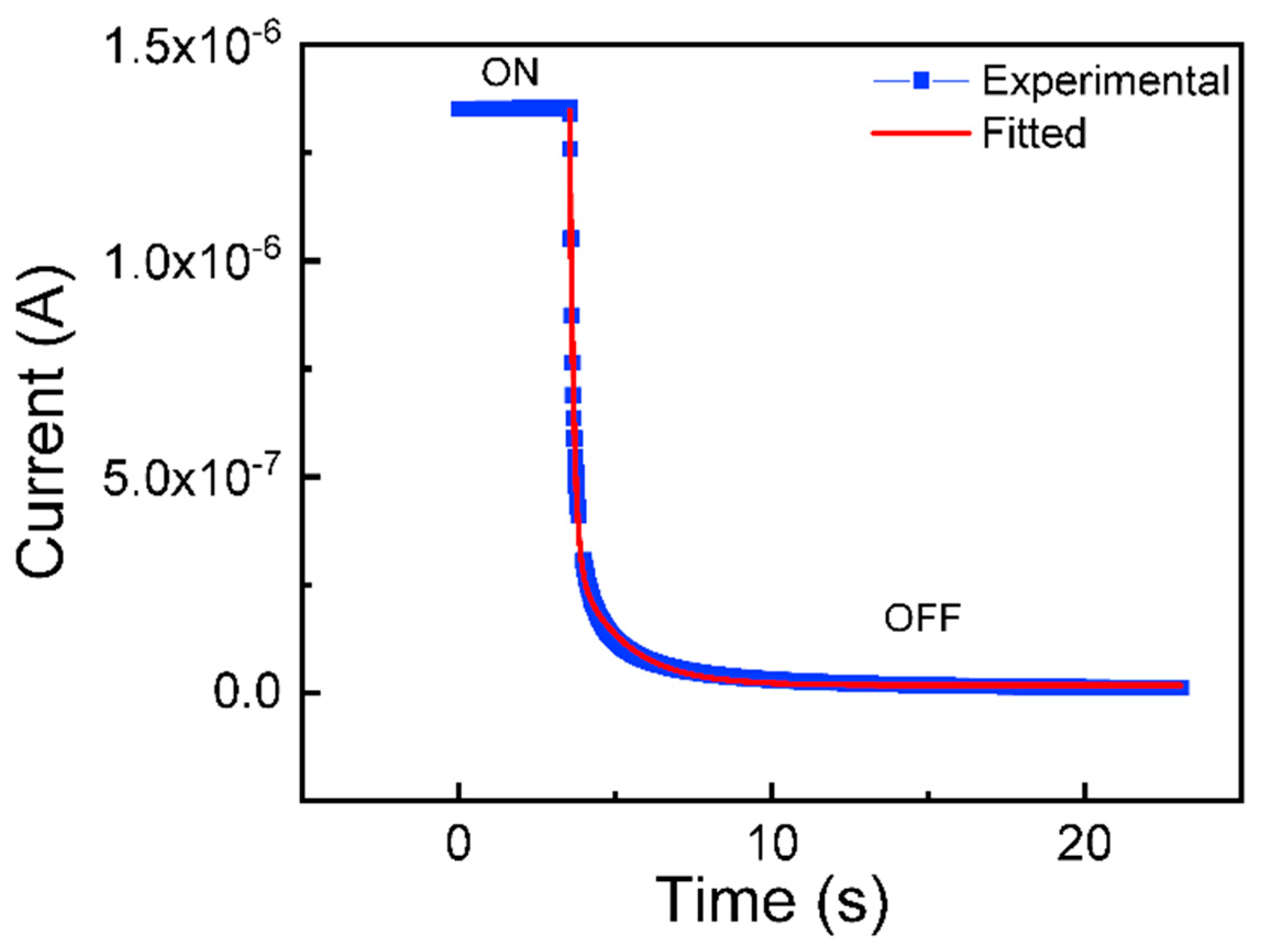
In the beginning, the photocurrent of the fabricated device was measured as a function of time. The photocurrent was collected using 5 V external bias applied to the device. An exponential decay kind of photocurrent curve was observed after switching off 250 nm wavelength as displayed in Figure 2. The power density of light was 400 µW/cm2. The photocurrent was observed to last for several seconds. Such a curve follows a biexponential equation [26,27]:
where I0 is the steady state current, A and B are fitting constants, and τ1 and τ2 are the fast and slow components of decay time, respectively. The data fitting of Equation (3) is shown as the red curve in Figure 1. The fast and slow decay times were acquired as 0.12 s and 1.58 s, respectively. Hence, the photocurrent persisted for a longer time in Ga2O3 material. Usually, sub-bandgap states are responsible for persistent photocurrent in the materials.
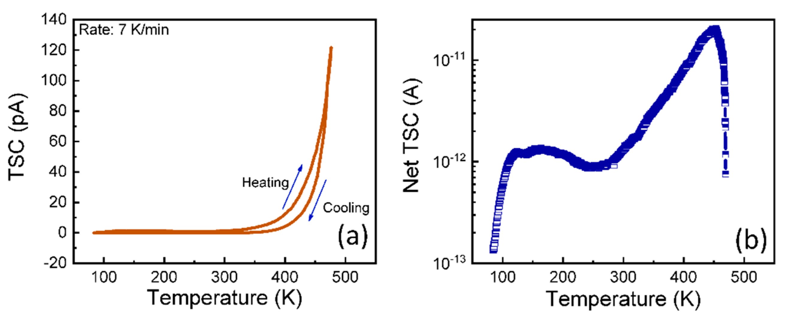
Figure 3a depicts the typical heating and cooling curves obtained from the TSC measurement of the β-Ga2O3 thin film. A clear difference between both of the curves was observed at about 400 K temperature. Such a difference in the cooling and heating curves was indicative of the appearance of a peak. However, other peaks may also have been present in the TSC which were relatively less contributary to the persistent photocurrent. Therefore, net TSC was calculated to investigate all the contributing peaks. It was defined as the difference between the total TSC and the dark current. Figure 3b depicts the net TSC spectrum which possessed two broad peaks centered near about 125 and 425 K temperature. The characteristic peak appearing at the higher temperature was one order of magnitude higher current than the other peak. The broad TSC peaks appeared due to the overlapping of several recombination centers.
The characteristic information of an individual trap can be obtained theoretically as well as experimentally. For theoretical calculation, the TSC peak was fitted with the Gaussian functions, and the activation energies could be calculated corresponding to characteristic peak temperature using Equation (2). However, two different procedures can be devised for experimentally resolving the broad spectrum without changing the occupation function. In the first approximation method, optical injection was performed at a particular temperature that was low enough for a characteristic trap so that it could not release the electron or hole. Then, the sample was heated with a constant heating rate to obtain the individual peak.
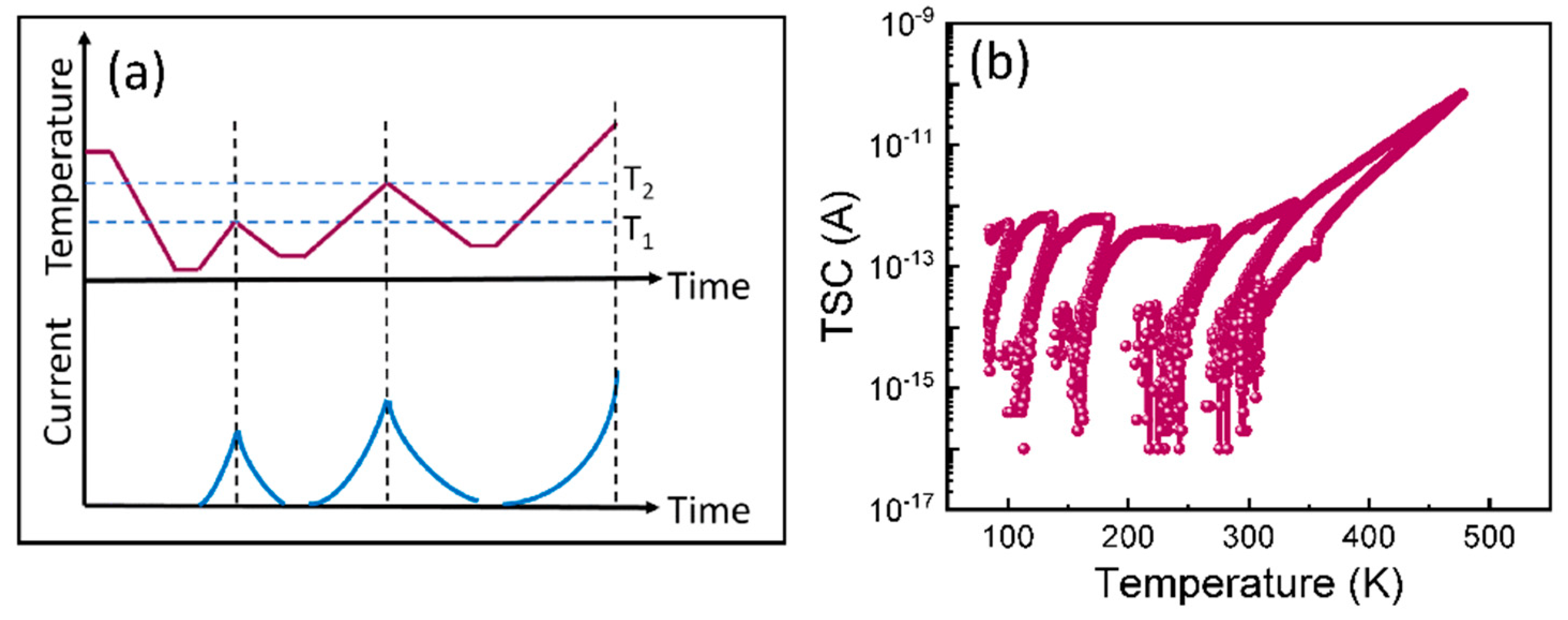
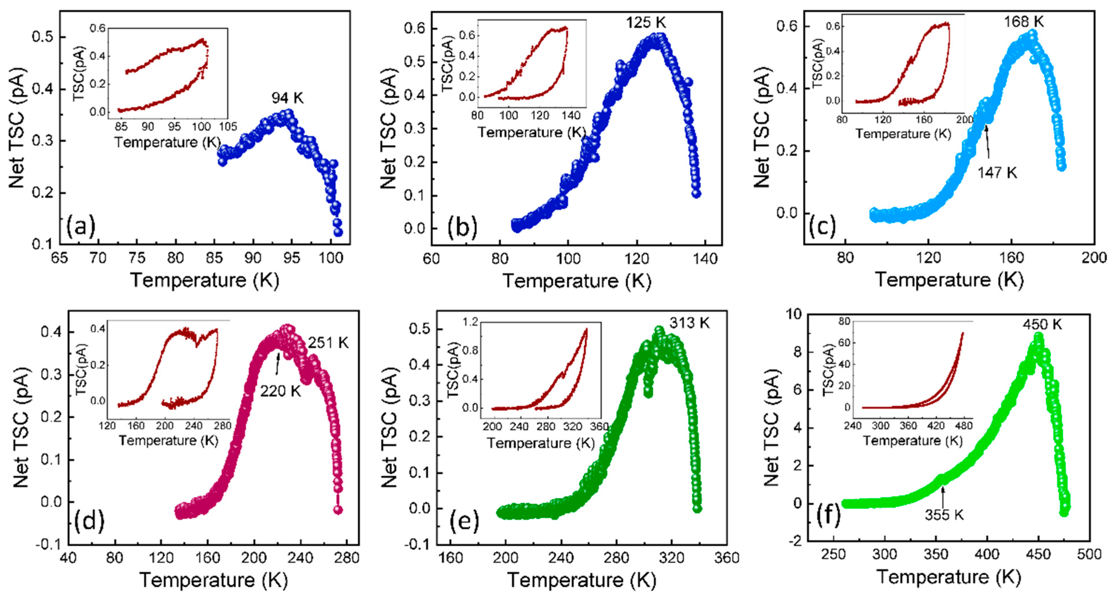
The second approximation method is known as fractional emptying of traps by subsequent heating and cooling cycles. The process flow for the fractional emptying method is shown in Figure 4a where T1 and T2 denote the characteristic temperature of an individual peak. The temperature was gradually increased and decreased with the same ramp rate to maintain the reversibility of the process. The temperature zone for each heating and cooling cycle was estimated using the help of the net TSC distribution so that the density of traps corresponding to the higher temperatures remained almost unchanged. Figure 4b displays all the fractionally resolved peaks of the TSC spectrum, where each temperature zone corresponded to a trap in the thin film. Six temperature zones were recorded for both the broad peaks. Furthermore, net TSC was calculated for each temperature zone to identify the peak maxima.
The net TSC spectra of all the traps are shown in Figure 5a–f. The insets of Figure 5a–f are the heating and cooling curves of corresponding traps. In some temperature zones, double temperature peaks were also identified. Three such temperature zones in the ranges of 125–170 K, 170–270 K, and 300–473 K were observed. The observation of double peaks resulted from the unintentional depopulation of two overlapped trap levels. Therefore, there was a total of nine peaks whose characteristic maxima were situated at 94, 125, 147, 168, 220, 251, 313, 355, and 450 K. The activation energies corresponding to all aforementioned peak maxima were calculated using Equation (2). The calculated approximate activation energies were 0.16, 0.23, 0.28, 0.33, 0.45, 0.52, 0.68, 0.78, and 1.03 eV, respectively. All these trap levels and their activation energies are also tabulated in Table 1. The subscripts a and b in the nomenclature of traps denote the low-temperature and high-temperature broad peaks of the net TSC spectrum.
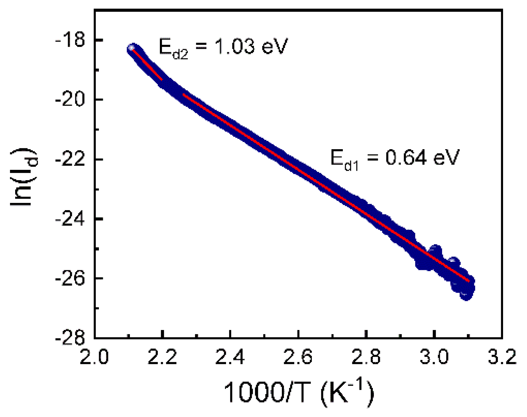
The Arrhenius method is also a technique for evaluating the activation energy of a trap level in the materials conventionally. It is calculated using the Arrhenius plot which is a graph between lnI and 1/T of the dark current. The activation energy is calculated using the relation [25]:
where k is the Boltzmann constant, and the slope is calculated from the linear fitting of the Arrhenius plot. The Arrhenius plot of β-Ga2O3 thin film is shown in Figure 6 using the dark current. Two linear regions were observed in the plot. The activation energies corresponding to both linear regions were 0.64 (Ed1) and 1.03 (Ed2) eV. The activation energies of traps Ed1 and Ed2 are similar to the energies of the traps Eb1 and Eb2 obtained from the TSC method.
It is important to mention here that different growth techniques and growth conditions may result in different combinations of defect levels. Even a trap level originating from the same impurity or point defect can give a slight energy shift. However, most of the traps obtained in the PLD-grown thin films were similar to the reported traps in β-Ga2O3 thin films and single crystals using different techniques. Wang et al. reported the deep defect levels at 0.105, 0.43, 0.49, 0.52, 0.56, 0.62, 0.84, 0.91, and 0.99 eV in the PLD-grown thin films by TSC and TSDC methods [18]. In our work, some new deep levels were observed, and some of the reported traps were not observed. The traps with activation energies 0.105, 0.49, 0.56, and 0.91 eV were not observed, whereas 0.16, 0.23, and 0.33 eV were observed. The origin of some of the observed trap levels can be proposed using the earlier reports as listed in Table 1. In the present work, unintentional external impurities such as N, Co, Fe, and Ti were present. Structural disorder also contributes to the creation of defects in thin films [20]. The origin of other traps of activation energies 0.16, 0.28, and 0.45 eV are still unknown. The trap level at 0.28 eV activation energy was also reported in Czochralski-grown single crystals [18]. Among all the observed traps, the deep-level trap of energy 1.03 eV was the dominant trap in the β-Ga2O3 thin films.
4. Conclusions
Thermally stimulated current spectroscopy was used to investigate deep-level traps in PLD-grown β-Ga2O3 thin films. Various trap levels of activation energies ranging from 0.16 to 1.03 eV were obtained. In the present work, some of the earlier reported traps in β-Ga2O3 thin films were not observed. However, some new trap levels were identified in the thin films. A deep-level trap of activation energy 1.03 eV was found to be the dominant trap in β-Ga2O3 that contributed to persistent photocurrent.
Author Contributions
Conceptualization, B.R.T.; methodology, B.R.T., M.-M.Y. and M.A.; validation, B.R.T., M.-M.Y., M.A. and R.S.; formal analysis, B.R.T.; investigation, B.R.T.; resources, M.A. and R.S.; data curation, B.R.T.; writing—original draft preparation, B.R.T.; writing—review and editing, B.R.T., M.-M.Y., M.A. and R.S.; supervision, M.A. and R.S.; funding acquisition, B.R.T. and R.S. All authors have read and agreed to the published version of the manuscript.
Funding
This research was funded by Department of Science and Technology (DST), India and British Council, UK under the Newton-Bhabha Ph.D. programme (Award No-DST/INSPIRE/NBHF/2018/1). R.S. acknowledges the Department of Science and Technology (DST), India for partial financial support for this work under BRICS Cooperation scheme DST/IMRCD/BRICS/Pilot Call 3/GaO-Nitrides/2019).
Acknowledgments
B.R.T. and R.S. would like to acknowledge Late Vinay Gupta, Department of Physics, University of Delhi for providing thin film growth facility and Nano research facility, IIT Delhi for providing device fabrication facilities, and M.A. would also like to acknowledge EPSRC (EP/P025803/1) for partial financial support.
Conflicts of Interest
The authors declare no conflict of interest.
References
- Higashiwaki, M.; Sasaki, K.; Kuramata, A.; Masui, T.; Yamakoshi, S. Development of gallium oxide power devices. Phys. Status Solidi A 2014, 211, 21–26. [Google Scholar] [CrossRef]
- Higashiwaki, M.; Sasaki, K.; Murakami, H.; Kumagai, Y.; Koukitu, A.; Kuramata, A.; Masui, T.; Yamakoshi, S. Recent progress in Ga2O3power devices. Semicond. Sci. Technol. 2016, 31, 034001. [Google Scholar] [CrossRef]
- Pearton, S.J.; Yang, J.; Cary, P.H., IV; Ren, F.; Kim, J.; Tadjer, M.J.; Mastro, M.A. A review of Ga2O3 materials, processing, and devices. Appl. Phys. Lett. 2018, 5, 011301. [Google Scholar]
- Sheoran, H.; Tak, B.R.; Manikanthababu, N.; Singh, R. Temperature-Dependent Electrical Characteristics of Ni/Au Vertical Schottky Barrier Diodes on β-Ga2O3 Epilayers. ECS J. Solid State Sci. Technol. 2020, 9, 055004. [Google Scholar] [CrossRef]
- Zhang, H.; Yuan, L.; Tang, X.; Hu, J.; Sun, J.; Zhang, Y.; Zhang, Y.; Jia, R. Progress of Ultra-Wide Bandgap Ga2O3 Semiconductor Materials in Power MOSFETs. IEEE Trans. Power Electron. 2020, 35, 5157–5179. [Google Scholar] [CrossRef]
- Hou, X.; Zou, Y.; Ding, M.; Qin, Y.; Zhang, Z.; Ma, X.; Tan, P.; Yu, S.; Zhou, X.; Zhao, X.; et al. Review of polymorphous Ga2O3 materials and their solar-blind photodetector applications. J. Phys. D Appl. Phys. 2020, 54, 043001. [Google Scholar] [CrossRef]
- Bosi, M.; Mazzolini, P.; Seravalli LFornari, R. Ga2O3 polymorphs: Tailoring the epitaxial growth conditions. J. Mater. Chem. C 2020, 8, 10975–10992. [Google Scholar] [CrossRef]
- Manikanthababu, N.; Tak, B.R.; Prajna, K.; Sarkar, S.; Asokan, K.; Kanjilal, D.; Barman, S.R.; Singh RPanigrahi, B.K. Swift heavy ion irradiation-induced modifications in the electrical and surface properties of β-Ga2O3. Appl Phys. Lett. 2020, 117, 142105. [Google Scholar] [CrossRef]
- Tao, X. Bulk gallium oxide single crystal growth. J. Semicond. 2019, 40, 010401. [Google Scholar] [CrossRef]
- Baldini, M.; Galazka, Z.; Wagner, G. Recent progress in the growth of β-Ga2O3 for power electronics applications. Mater. Sci. Semicond. Process. 2018, 78, 132–146. [Google Scholar] [CrossRef]
- Galazka, Z.; Uecker, R.; Irmscher, K.; Albrecht, M.; Klimm, D.; Pietsch, M.; Brützam, M.; Bertram, R.; Ganschow, S.; Fornari, R. Czochralski growth and characterization of β-Ga2O3 single crystals. Cryst. Res. Technol. 2010, 45, 1229–1236. [Google Scholar] [CrossRef]
- Kuramata, A.; Koshi, K.; Watanabe, S.; Yamaoka, Y.; Masui, T.; Yamakoshi, S. High-quality β-Ga2O3 single crystals grown by edge-defined film-fed growth. Jpn. J. Appl. Phys. 2016, 55, 1202A2. [Google Scholar] [CrossRef]
- Kim, J.; Pearton, S.J.; Fares, C.; Yang, J.; Ren, F.; Kim, S.; Polyakov, A.Y. Radiation damage effects in β-Ga2O3 materials and devices. J. Mater. Chem. C 2019, 7, 10–24. [Google Scholar] [CrossRef]
- Tak, B.R.; Garg, M.; Dewan, S.; Torres-Castanedo, C.G.; Li, K.-H.; Gupta, V.; Li, X.; Singh, R. High-temperature photocurrent mechanism of β-Ga2O3 based metal-semiconductor-metal solar-blind photodetectors. J. Appl. Phys. 2019, 125, 144501. [Google Scholar] [CrossRef] [Green Version]
- Zheng, Y.; Swinnich, E.; Seo, J.-H. Investigation of Thermal Properties of β-Ga2O3 Nanomembranes on Diamond Heterostructure Using Raman Thermometry. ECS J. Solid State Sci. Technol. 2020, 9, 055007. [Google Scholar] [CrossRef]
- Zhang, Z.; Farzana, E.; Arehart, A.R.; Ringel, S.A. Deep level defects throughout the bandgap of (010) β-Ga2O3 detected by optically and thermally stimulated defect spectroscopy. Appl Phys. Lett 2016, 108, 052105. [Google Scholar] [CrossRef]
- Neal, A.T.; Mou, S.; Lopez, R.; Li, J.V.; Thomson, D.B.; Chabak, K.D.; Jessen, G.H. Incomplete Ionization of a 110 meV Unintentional Donor in β-Ga2O3 and its Effect on Power Devices. Sci. Rep.-UK 2017, 7, 13218. [Google Scholar]
- Wang, B.G.; Look, D.; Leedy, K. Deep level defects in β-Ga2O3 pulsed laser deposited thin films and Czochralski-grown bulk single crystals by thermally stimulated techniques. J. Appl. Phys. 2019, 125, 105103. [Google Scholar] [CrossRef]
- Tadjer, M.J.; Koehler, A.D.; FreitasJr, J.A.; Gallagher, J.C.; Specht, M.C.; Glaser, E.R.; Hobart, K.D.; Anderson, T.J.; Kub, F.J.; Thieu, Q.T.; et al. High resistivity halide vapor phase homoepitaxial β-Ga2O3 films co-doped by silicon and nitrogen. Appl. Phys. Lett. 2018, 113, 192102. [Google Scholar] [CrossRef]
- Fiedler, A.; Schewski, R.; Baldini, M.; Galazka, Z.; Wagner, G.; Albrecht, M.; Irmscher, K. Influence of incoherent twin boundaries on the electrical properties of β-Ga2O3 layers homoepitaxially grown by metal-organic vapor phase epitaxy. J. Appl. Phys. 2017, 122, 165701. [Google Scholar] [CrossRef]
- Ingebrigtsen, M.E.; Varley, J.B.; Kuznetsov, A.Y.; Svensson, B.G.; Alfieri, G.; Mihaila, A.; Badstübner, U.; Vines, L. Iron and intrinsic deep level states in β-Ga2O3. Appl. Phys. Lett. 2018, 112, 042104. [Google Scholar] [CrossRef] [Green Version]
- Zimmermann, C.; Frodason, Y.K.; Barnard, A.W.; Varley, J.B.; Irmscher, K.; Galazka, Z.; Karjalainen, A.; Meyer, W.E.; Auret, F.D.; Vines, L. Ti- and Fe-related charge transition levels in β-Ga2O3. Appl. Phys. Lett. 2020, 116, 072101. [Google Scholar] [CrossRef]
- Irmscher, K.; Galazka, Z.; Pietsch, M.; Uecker, R.; Fornari, R. Electrical properties of β-Ga2O3 single crystals grown by the Czochralski method. J. Appl. Phys. 2011, 110, 063720. [Google Scholar] [CrossRef]
- Sze, S.M.; Ng, K.K. Physics of Semiconductor Devices; John Wiley & Sons: Hoboken, NJ, USA, 2007. [Google Scholar]
- Braunlich, P. Thermally Stimulated Relaxation in Solids; Springer: Berlin/Heidelberg, Germany; New York, NY, USA, 1979. [Google Scholar]
- Tak, B.R.; Yang, M.-M.; Lai, Y.-H.; Chu, Y.-H.; Alexe, M.; Singh, R. Photovoltaic and flexible deep ultraviolet wavelength detector based on novel β-Ga2O3/muscovite heteroepitaxy. Sci. Rep. 2020, 10, 16098. [Google Scholar] [CrossRef] [PubMed]
- Bhatnagar, A.; Kim, Y.H.; Hesse, D.; Alexe, M. Persistent Photoconductivity in Strained Epitaxial BiFeO3 Thin Films. Nano Lett. 2014, 14, 5224–5228. [Google Scholar] [CrossRef] [Green Version]
Figure 1.
Band diagram of: (a) trap filling via optical injection of charge carriers; (b) after complete trapping; (c) under thermal release of carriers.
Figure 1.
Band diagram of: (a) trap filling via optical injection of charge carriers; (b) after complete trapping; (c) under thermal release of carriers.

Figure 2.
The decay of photocurrent as a function of time after turning off the illumination. The red curve indicates the fitting using biexponential equation.
Figure 2.
The decay of photocurrent as a function of time after turning off the illumination. The red curve indicates the fitting using biexponential equation.

Figure 3.
(a) Heating and cooling curve of TSC at 7 K/min heating rate, (b) net TSC spectrum of the β-Ga2O3 thin film.
Figure 3.
(a) Heating and cooling curve of TSC at 7 K/min heating rate, (b) net TSC spectrum of the β-Ga2O3 thin film.

Figure 4.
(a) Process flow of fractional emptying method for TSC peak resolution and (b) resolved peaks of TSC spectrum for all the traps.
Figure 4.
(a) Process flow of fractional emptying method for TSC peak resolution and (b) resolved peaks of TSC spectrum for all the traps.

Figure 5.
Net TSC peaks of all the traps with characteristic peak temperature (a) 94 K (b) 125K (c) 168 K, (d) 220 and 251 K, (e) 313 K and (f) 450 K.
Figure 5.
Net TSC peaks of all the traps with characteristic peak temperature (a) 94 K (b) 125K (c) 168 K, (d) 220 and 251 K, (e) 313 K and (f) 450 K.

Figure 6.
Arrhenius plot of dark current.


Table 1.
List of traps and their activation energies in β-Ga2O3 thin film using TSC method.
| Trap | Peak Temperature (K) | Activation Energy (eV) |
|---|---|---|
| Ea1 | 94 | 0.16 |
| Ea2 | 125 | 0.23 |
| Ea3 | 147 | 0.28 |
| Ea4 | 168 | 0.33 |
| Ea5 | 220 | 0.45 |
| Ea6 | 251 | 0.52 |
| Eb1 | 313 | 0.68 |
| Eb2 | 355 | 0.78 |
| Eb3 | 450 | 1.03 |
Publisher’s Note: MDPI stays neutral with regard to jurisdictional claims in published maps and institutional affiliations. |
© 2021 by the authors. Licensee MDPI, Basel, Switzerland. This article is an open access article distributed under the terms and conditions of the Creative Commons Attribution (CC BY) license (https://creativecommons.org/licenses/by/4.0/).
Share and Cite
MDPI and ACS Style
Tak, B.R.; Yang, M.-M.; Alexe, M.; Singh, R. Deep-Level Traps Responsible for Persistent Photocurrent in Pulsed-Laser-Deposited β-Ga2O3 Thin Films. Crystals 2021, 11, 1046. https://0-doi-org.brum.beds.ac.uk/10.3390/cryst11091046
AMA Style
Tak BR, Yang M-M, Alexe M, Singh R. Deep-Level Traps Responsible for Persistent Photocurrent in Pulsed-Laser-Deposited β-Ga2O3 Thin Films. Crystals. 2021; 11(9):1046. https://0-doi-org.brum.beds.ac.uk/10.3390/cryst11091046
Chicago/Turabian StyleTak, Bhera Ram, Ming-Min Yang, Marin Alexe, and Rajendra Singh. 2021. "Deep-Level Traps Responsible for Persistent Photocurrent in Pulsed-Laser-Deposited β-Ga2O3 Thin Films" Crystals 11, no. 9: 1046. https://0-doi-org.brum.beds.ac.uk/10.3390/cryst11091046
Note that from the first issue of 2016, this journal uses article numbers instead of page numbers. See further details here.