1. Introduction
The use of GaN/InGaN material systems has been generally applied to light emitting diodes (LEDs) and blue laser diodes (LDs) and widely employed in many technologies, from general illumination to display and high-speed communications [
1]. Despite highly efficient devices in the blue emission regime, devices emitting at longer wavelengths such as green, yellow, amber, and red all suffer from much lower quantum efficiencies [
2]. One of the most significant issues with these longer wavelength devices is incorporating indium in alloy compositions greater than 25% without serious microstructural degradation. The low structural quality of high-In alloy compositions makes the realization of these long-wavelength emitters difficult [
3,
4]. The crystal quality of the alloy suffers with increasing In content due to a variety of issues, notably the large difference between desorption temperature of In and Ga and significant and increasing lattice mismatch between the underlying GaN buffer layer and the InGaN quantum wells (QWs) [
5].
A large and abrupt lattice constant mismatch between the thick GaN buffer and the InGaN epilayer generates a large biaxial compressive stress in the InGaN layer [
6]. These stresses then directly lead to a strained epilayer. To mitigate the issues arising from lattice mismatch, we employed substrates consisting of relaxed InGaN with a larger lattice constant provided by SOITEC. Relaxed substrates employ a larger lattice constant compared with GaN, which leads to a reduction in biaxial compressive stress for the subsequently grown InGaN epilayers, most notably the quantum wells (QWs) [
7]. During growth, the incorporation efficiency of In in an InGaN alloy steadily decreases with increasing strain and lattice mismatch due to the deformation energy from alloying the In atoms [
8,
9,
10]. This reduction in In incorporation efficiency with strain is known as the compositional pulling effect. Therefore, the reduction in strain directly leads to a higher In incorporation in the InGaN epilayer itself as a result of a reduction in this compositional pulling effect [
11]. As further evidence for this effect, a decrease in the measured piezoelectric field at equal In mole fractions can be seen for relaxed substrates compared with conventional ones [
12]. Strain reduction from use of relaxed substrates generates comparatively higher crystal quality in the high-In QW, resulting in higher PL efficiency than conventional GaN-on-sapphire growth [
13,
14].
One major roadblock to the realization of working, long-wavelength, and visible LEDs on these relaxed InGaN substrates is the poor crystal quality and morphology. V-defects are 3-dimensional defects with the form of inverted hexagonal pyramids, where the {10-11} crystallographic planes form the sidewalls of the pyramidal defect. V-defects widen, expanding in size, depending on growth conditions used [
15], leading to poor morphology as the material continues to grow epitaxially. Uncontrolled propagation of V-defects during growth creates large-scale defect regions of material [
16], which would likely preclude a working device. Since the growth substrates employed here are fabricated from an epitaxially grown InGaN film, they natively contain V-defects, which will increase in size during growth. V-defects need to be filled immediately during epitaxial growth to realize a flat layer. Additionally, interlayer schemes of GaN layers contained within an InGaN base layer have been reported to reduce other defects, retain 2D step-flow growth, and significantly improve material quality over a single thick InGaN layer [
17]. In our previous work, we have explored and developed an InGaN/GaN buffer/interlayer scheme similar to a superlattice (SL) with optimized buffer and interlayer thicknesses, temperatures, V/III ratio, and carrier gasses [
18]. These developments significantly improve the crystal quality for the base layer and allow the advantages of the relaxed InGaN substrate to be leveraged into devices.
We examine the application of these periodic InGaN/GaN base layer structures on relaxed substrates in the growth of
LEDs to enable emission across the entire visible spectra. Employing an InGaN/GaN interlayer structure with high temperature (HT) GaN interlayers, where the elevated temperature has shown to improve Ga surface diffusion and both fill pre-existing V-defects and suppress their subsequent formation [
18], we enable working
LED devices with appreciable electroluminescence emission across the visible range. For
LEDs grown on these InGaN/GaN base layers, a significant reduction in the V-defect density and an improvement to crystal quality results in appreciable electroluminescence readily visible even by eye. These resulting
LED devices were analyzed in terms of their emission spectra and current-voltage response to determine a baseline device performance and ensure diode-like behavior. Compared to previous devices grown on lower quality base layers, we enabled long-wavelength electroluminescence, showing significant increase in the emitted light intensity and achieving working
LED devices.
2. Materials and Methods
The semi-relaxed substrates used throughout this study are provided by SOITEC, a private industry partner, and will be referred to as “InGaNOS” substrates. The substrates consist of 490 × 490
m
InGaN mesas with 10
m cuts between them forming a grid, where the lattice constant and relaxation are tunable based on the substrate mesa size and In content. The mesas are 150 nm thick with a lattice constant of 3.205 Å for all samples examined here, with a buried oxide between the sapphire and mesas. These templates employ nominally 4% In, with relaxation of 54% that is tunable using SOITEC’s proprietary Smart-Cut technology. Structurally, the epi-ready InGaNOS substrates have 5 × 10
cm
pre-existing V-defects and (0002) X-ray reflections FWHM around 2600 arcsec as-received. More specific details on substrate processing, fabrication, and structural and optical quality can be found in ref. [
11].
Base layers and LEDs were grown by MOCVD at atmospheric pressure on the InGaNOS substrates using triethylgallium (TEGa), trimethylindium (TMIn), and ammonia (NH
) as the precursors for GaN and InGaN growth, disilane (Si
H
) and Bis(cyclopentadienyl) magnesium (Cp
Mg) as respective precursors for n- and p-type dopants, and nitrogen and hydrogen as carrier gasses. The Si concentration for the n-type InGaN/GaN:Si base layer doping is nominally 5 × 10
cm
. We employed an Mg concentration of 1.5 × 10
cm
for the p-type InGaN/GaN:Mg region doping. We investigated multiple LEDs, each with different emission wavelength, on the same base layers. Base layers were grown at a temperature of nominally 950
C for the InGaN regions and 1050
C for the GaN interlayers. This InGaN/GaN base layer is the n-contact layer for the subsequently grown LED device. For all samples, the HT GaN interlayers eliminated the pre-existing V-defects and prevented the creation of new ones. The structure and growth conditions of the base layer, as well as study of the V-defect elimination mechanism, are examined in great detail in prior work [
18]. Once base layers were grown, we regrew active regions (ARs) consisting of 5 periods of 2.8 nm thick InGaN QWs, 2 nm AlGaN cap layers with 10% Al content, and 10 nm GaN quantum barriers (QBs) consisting of a 4 nm lower temperature (LT) portion and 6 nm higher temperature (HT) portion. Details on the active region structure can be found elsewhere [
19]. The p-contact layer for both structures consisted of a 5-period Mg-doped InGaN/GaN (20 nm InGaN and 2 nm GaN interlayers) structure with a nominal thickness of 110 nm grown isothermally.
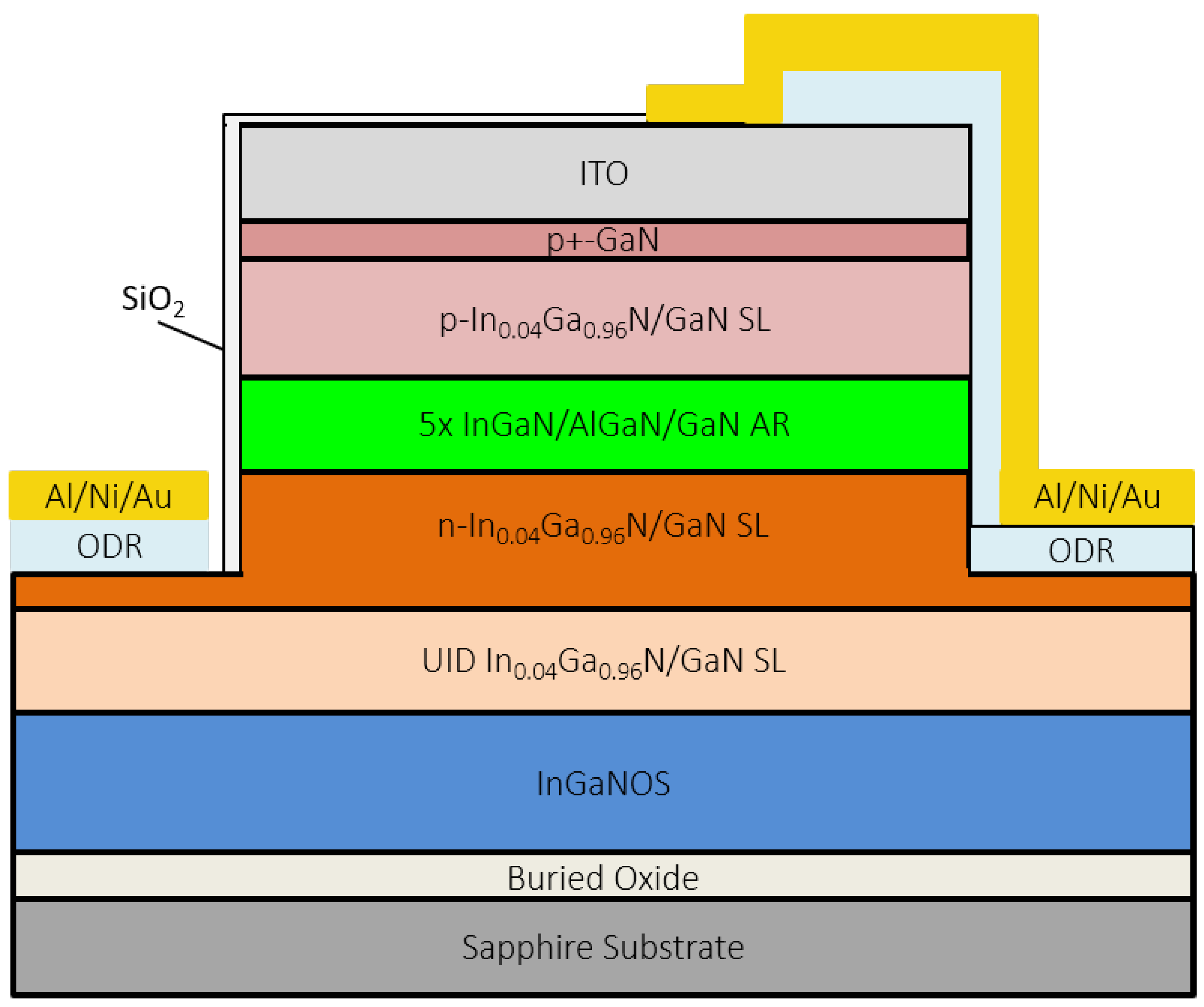
For processing the samples, the same
LED process was employed for all samples. First, aqua regia and solvent cleans were performed to remove any surface contamination, surface Mg, or growth residue. After cleaning, 110 nm of indium tin oxide (ITO) was deposited as a transparent conducting oxide (TCO) layer via electron beam deposition for use as a p-contact. The LED device mesas were then defined by reactive-ion etching (RIE), first using methane/hydrogen/argon plasma to etch the ITO, then using SiCl
to etch the III-Nitride epi down to the n-GaN layer in a self-aligned fashion. After etching, an omnidirectional reflector (ODR), consisting of three pairs of silicon dioxide (SiO
) and tantalum oxide (Ta
O
) layers was deposited followed by an aluminum oxide Al
O
capping layer by ion beam deposition (IBD). The periodic SiO
and Ta
O
layers act as a reflector for the sidewall while the Al
O
layer acts as a metal adhesion layer, allowing dielectric isolation and good adhesion for metal contacts to be later deposited on top of the ODR. Next, Atomic Layer Deposition (ALD) was used to deposit 50 nm of SiO
at 300
C as sidewall passivation. After ALD blanket deposition, areas of SiO
were removed using buffered hydrofluoric acid (BHF) to later deposit contacts there. Common p- and n-contact pads were composed of 500/100/500 nm of Al/Ni/Au using electron-beam deposition. A full schematic of the fabricated device structure can be seen in
Figure 1. Further detail on the full fabrication process can be found in prior works in greater detail [
20]. Electrical testing of the finished devices was performed using a Keithley source generator.
3. Results
To realize working LED devices with appreciable electroluminescence emission and operation lifetime, low defect density must be present in the epitaxy, especially when considering large defects such as V-defects or metallic In inclusions. Since the semi-relaxed InGaN substrates used here have a high density of V-defects, material quality must be significantly improved during the epitaxy to realize robust LED devices. In our previous work, we report on fully eliminating the V-defects in the InGaN base layers originating in the substrates through periodically growing high temperature (HT) GaN interlayers under partial H
carrier gas injection in the InGaN base layer, leading to significant structural improvement [
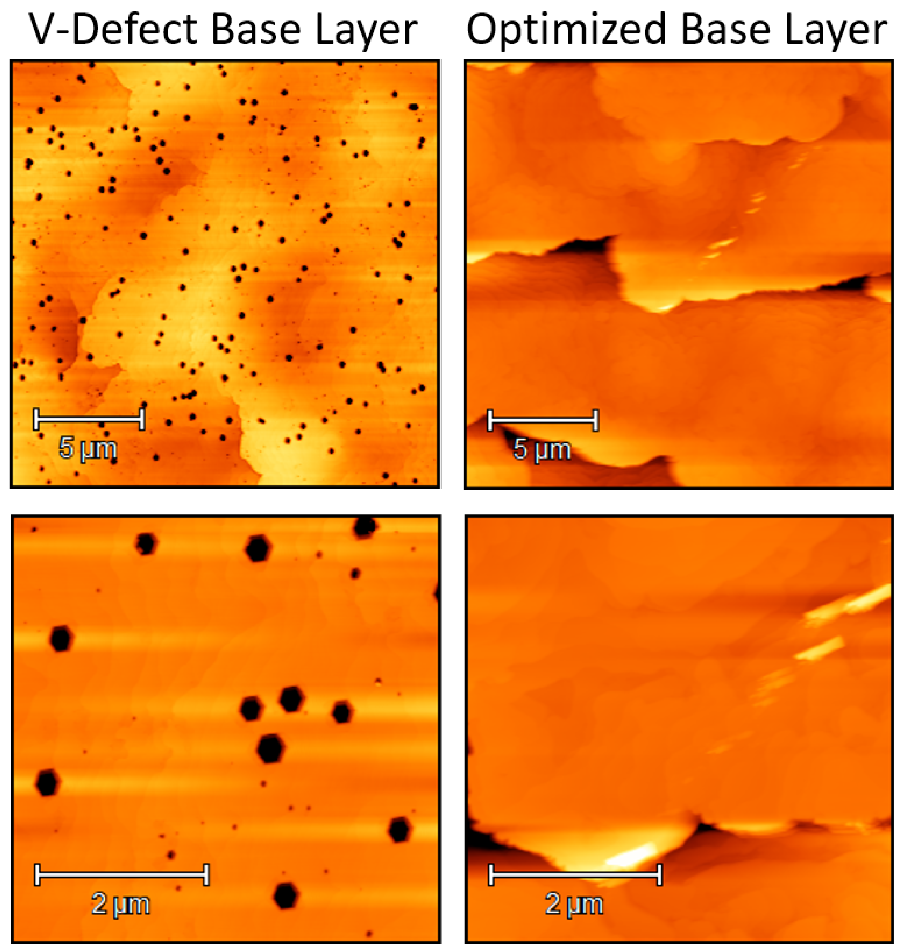
18]. This improvement can also be noted in
Figure 2, which clearly shows the full elimination of V-defects on the optimized base layer. The improved epitaxy methods and the elimination of V-defects allow the benefits of the relaxed substrate to be leveraged into LED devices. Notably, the electrical and optical characteristics of the devices significantly improved when V-defects were eliminated, allowing a variety of EL emission wavelengths to be demonstrated.
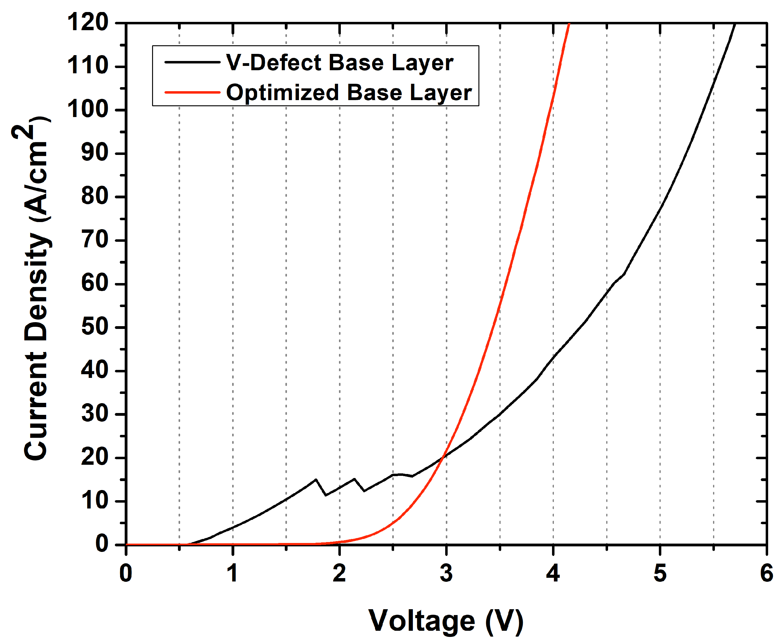
Electrical characteristics were compared between LEDs grown on early development, V-defect base layers, and optimized base layers free from V-defects through their current density-voltage (JV) behavior.
Figure 3 compares two devices to examine their electrical behavior relative to each other. These devices only differ in the growth of the base layer, where the active region and p-type layers are otherwise equivalent. For both samples, we can compare the leakage current density at a forward voltage of 2.0 V, as it is below the turn-on voltage and large enough to generate a measurable forward leakage current for both samples. It is clear that, even at a low forward bias of 2 V, significant current density measuring in the tens of A/cm
is achieved in the
LED device with the V-defect layer. Specifically, the
LED device fabricated with the high V-defect density base layer yields a leakage current density of 13.3 A/cm
while the device fabricated with the optimized base layer yields 0.629 A/cm
at 2.0 V of forward bias. The
LED device with the optimized base layer displays JV behavior more typical of an LED. The optimized base layer sample has a much lower forward leakage current and a well-defined turn-on with a linear region in the current density-voltage response.
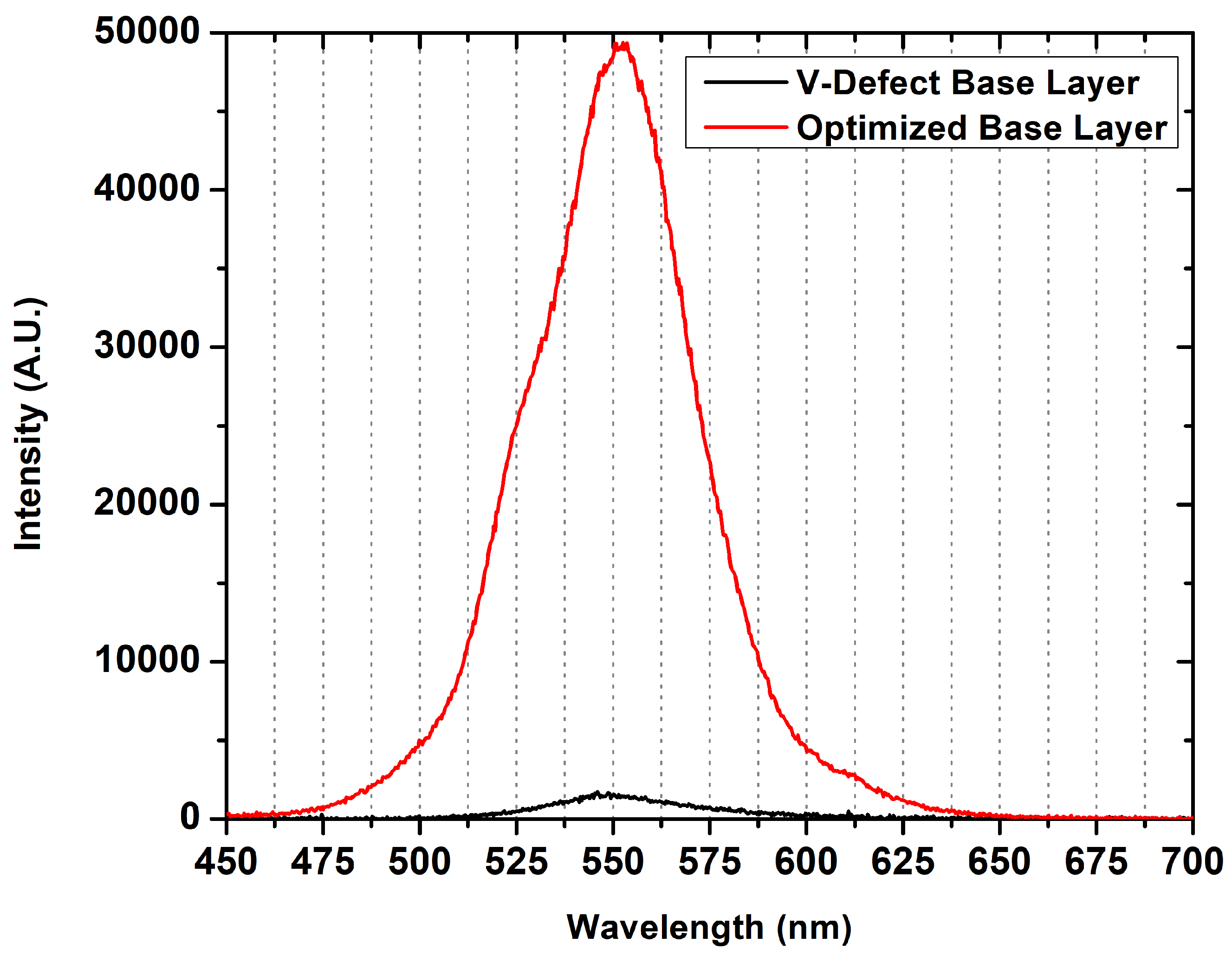
The electroluminescence emission spectra of
LED devices fabricated from the two types of base layers examined here, V-defect and optimized, were also compared.
Figure 4 contains the electroluminescence spectra of the same two devices present in
Figure 3 in order to make a clear comparison between them. The peak wavelength of the
LEDs grown on V-defect base layer and optimized base layers are nearly identical, 549 and 551 nm, respectively, making the comparison between the samples reasonable. Under identical injection conditions of 35 A/cm
, identical device size of 80 × 80
m
, and identical measurement setup, the
LED fabricated from the optimized base layer caused the absolute EL intensity to increase by more than an order of magnitude with a much more well-defined Gaussian peak. The FWHM of the V-defect base layer and optimized base layer
LEDs’ emission peak was 41 nm and 49 nm, respectively. A small shoulder can be noted in the spectra for the device with the optimized base layer, which we attributed to In fluctuation in the QW at this long wavelength emission.
Beyond significantly improving to the electrical characteristics and performance of
LED devices at a given wavelength, the optimized base layer design enables the realization of a broad range of emission wavelengths, from cyan to deep red. The emission of the devices was generally controlled through QW growth temperature to achieve the desired emission wavelength.
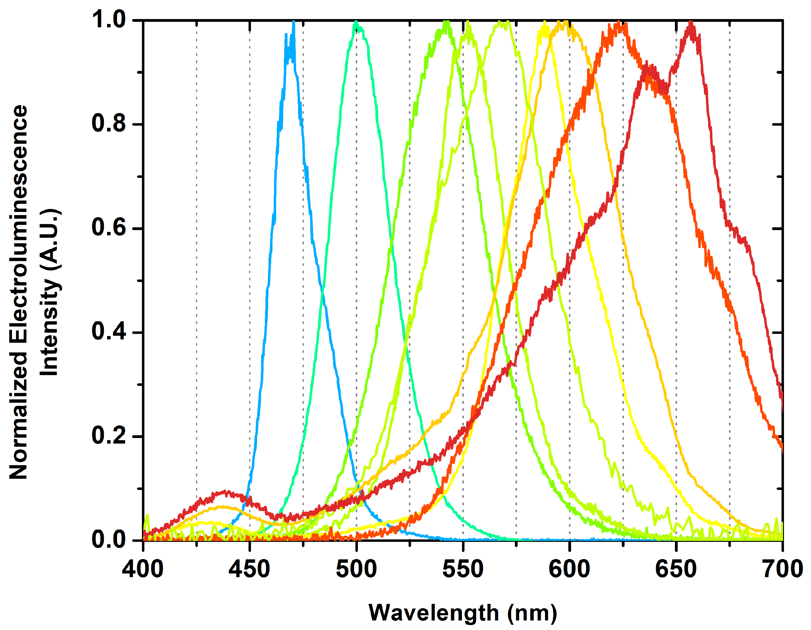
Figure 5 shows the normalized EL emission spectra of nine selected
LED devices containing optimized base layers with peak emission wavelength ranging from 470 nm to 645 nm. These spectra were taken at equal current density, 20 A/cm
, with the exception of the 470 nm emitting device taken at 30 A/cm
to achieve adequate light collection on an early LED sample. Generally, the full-width at half maximum (FWHM) of the emission peaks steadily increases with increasing wavelength emission. For devices with a peak emission at or below 580 nm, a single peak is observed with a relatively Gaussian shape. For devices with peak emission above 580 nm, multiple peaks can be seen in the emission as "shoulders" to the main peak or as closely grouped peaks that overlap. We attributed the broadening emission to the likely microstructural inhomogeneity in the highest indium content samples. Similarly, the FWHM of the EL emission peak to increase with wavelength, from 23 nm for the 470 nm emitting device to 89 nm for the multi-peak 645 nm emitting device.
4. Discussion
The significant improvement to
LED devices in terms of diode behavior, leakage current, and electroluminescence intensity can be attributed to the higher quality epitaxy, specifically from the elimination of V-defects in the base layer and resulting improvements to layer morphology. V-defects in the base layer must be managed to avoid propagation through the epitaxial structure to create large defect regions, or from forming leakage pathways. Since the majority of V-defects originate in the substrate, these V-defects propagate through the entire device structure beginning at the n-type base layer through the active region and into the p-type region, widening as growth proceeds. Since V-defects form and widen from kinetically-limited growth, they can be filled at higher growth temperatures with different V/III ratios and carrier gasses such that there is sufficient mass transport to the V-defect sidewalls (
Figure 2). The V-defects in these devices are eliminated in the intrinsic and n-type regions when the lateral ingrowth of the defects becomes dominant over widening and propagation, consequently causing planarization of the growth surface. Eliminating the V-defects improves the electrical performance of microLEDs fabricated using these base layers by directly leading to a significant reduction in leakage current and improving diode behavior. In the same way, EL emission intensity of a
LED device with an optimized base layer also increases by over an order of magnitude—a factor of 30—at equivalent current density compared with a
LED device on a V-defect base layer (
Figure 4).
A significant improvement to electrical performance can be attributed to the general improvement to crystal morphology by elimination of V-defects, optimizing growth conditions, and elimination of leakage paths. As shown in
Figure 3, the leakage current density at voltages below the turn-on voltage measures in the tens of A/cm
for the device on the V-defect buffer as a result of a high V-defect density propagating from the substrate and its detrimental effect on morphology. Here, turn-on voltage is defined as the voltage where light can be detected initially, corresponding to when the JV response curve becomes superlinear beyond the leakage current regime. The high leakage currents demonstrated here below device turn-on recombine nonradiatively, quickly causing these devices to fail under operation through self-destruction of the metal contacts or open-circuit failure within the device. For these initial devices with poor morphology and unoptimized growth conditions, many of the devices on the processed sample would fail immediately beyond moderate voltages (in the 4–5 V range), or alternatively after a relatively short period of continued operation on the order of seconds to minutes. Conversely, the optimized base layer free of V-defects yielded devices with much lower leakage currents and improved diode behavior. These devices had a somewhat high series resistance represented by the inverse of the slope of the linear region in
Figure 3, but it is greatly reduced compared with the
LED on the V-defect base layer. While some leakage current is naturally still present even in the V-defect-free
LED, this is attributed to other non-radiative recombination centers that arise from impurities or defects from crystal growth. Additionally, these devices were capable of operation at forward biases exceeding 7 V even after multiple testing cycles, as well as continuous operation on the order of hours without failure. The trend of a marked lifetime difference between devices grown on V-defect base layers and optimized base layers held true for all wavelength devices examined. The optimized base layer
LED device displays a lower operating voltage, lower series resistance, lower leakage current, and more robust lifetime and operation. In nearly all metrics, the electrical performance of
LED devices is improved.
In a similar vein, the optical characteristics of the device also significantly improve with optimization of the base layer. Electroluminescence spectra of identically sized
LED devices grown on the optimized base layer under identical current injection, measurement geometry, and integration time are presented in
Figure 4, where the EL intensity of the
LED device on the optimized base layer increases by a factor of 30 compared with the V-defect base layer, indicating a marked increase in the radiative efficiency of the device. Additionally, these two devices have a nearly identical emission wavelength, making the devices comparable. A small shoulder peak was visible in the peak from the optimized base layer
LED, which we attributed to minor In fluctuation in the QW from the high-In content required to achieve this long wavelength. This, in turn, also causes the FWHM to increase with increasing EL emission intensity, as seen in these samples. Generally, improvements in
LED devices resulting from an optimized base layer enable a wide variety of
LED devices to be realized with high brightness.
The emission wavelengths represented by the devices displayed in
Figure 5 are remarkable for two reasons: first, the range of wavelengths represented is quite wide, and second, the emission range extends quite far into the long-wavelength visible regime compared with typical III-nitride devices. At a moderate operation current density of 20 A/cm
, devices with a 175 nm range of peak wavelengths have been realized, covering most of the visible spectrum including the entire long-wavelength red area. The reduction of the compositional pulling effect by the semi-relaxed substrate and optimized base layer, as mentioned above, improved In incorporation in the QW. This development enabled peak EL emission into the amber, red, and crimson regime. Devices with peak EL emission in the red regime, specifically at or above 600 nm, are typically extraordinarily difficult to realize with III-nitride materials due to the requirement of low temperature during QW growth for sufficient In incorporation [
21,
22]. The realization of working devices with measurable emission is then inhibited as a result of increasing defect density, In segregation, and poor growth morphology [
23]. By contrast, here, we were able to employ higher growth temperatures due to the higher In incorporation in the QW enabled by the semi-relaxed substrates and reduction of the compositional pulling effect. This same effect enables the use of higher QW growth temperatures while maintaining the same emission wavelength.
As peak emission wavelength becomes longer, and the FWHM widens, as expected from increasing In fluctuation. Additionally, a small peak, around 425 nm, becomes more intense at longer wavelengths. We attributed this peak to charge injection through the low density of V-defects commonly generated in the lower QWs [
24] into the V-defect-free n-InGaN buffer region where they recombine. The V-defects allow charge transport through the sidewall where the polarization barrier is reduced and the path conductivity is increased [
25,
26]. At very long wavelengths, larger In fluctuations can be seen as small shoulders in the 620 nm emission
LED and as a close cluster of multiple peaks in the 645 nm emission
LED. At the longest visible wavelengths, some In phase separation in the QW becomes difficult to avoid. These issues arising from high-In QW growth—namely, extended defect generation, In segregation, and related effects such as V-defect sidewall injection leakage—must be mitigated through optimization of the growth conditions in the QW and QW capping layers. Since defect generation is predominately in the form of V-pits, a similar growth approach to that used in the V-defect-free base layer could be applied to the QW. These growth conditions would suppress V-defect nucleation and close any V-defects that happen to form, as previously seen in the predominately InGaN base layer. At the same time, the leakage current from the V-defect sidewall into the base layer causing undesired short-wavelength emission would be eliminated. For suppression of In segregation, further development of the AlGaN capping layer to prevent In desorption during growth and thermal protection during later high temperature layer growth is necessary for a more homogeneous alloy layer. Since low growth temperatures must be used for increasingly higher In QW growth, but the GaN QB growth remains at the same temperature, the temperature difference between the two layers increases with increasing In content. The role of the QW capping layer then becomes even more crucial with longer wavelength LEDs requiring higher QW In contents. The development of both of these aspects of
LED devices has already begun. Despite these difficulties, the current realization of a III-nitride device emitting such long wavelengths with appreciable electroluminescence emission at a moderate current density has been achieved using these semi-relaxed substrates and optimized base layers, a feat not typically achieved with conventional GaN-on-sapphire growth.


 ,
, 


