Article

Characterization of Structural Defects in (Cd,Zn)Te Crystals Grown by the Travelling Heater Method

1
Freiburg Materials Research Center FMF, 79104 Freiburg, Germany
2
Research and Development Institute for Launch Complexes NIISK, 119526 Moscow, Russia
3
Institute of Solid State Physics of Russian Academy of Sciences, 142432 Chernogolovka, Russia
4
Fraunhofer Institute for Applied Solid State Physics IAF, 79108 Freiburg, Germany
5
Institute for Photon Science and Synchrotron Radiation (IPS), Karlsruhe Institute of Technology, 76344 Karlsruhe, Germany
6
Crystallography, Institute of Earth and Environmental Sciences, University of Freiburg, 79104 Freiburg, Germany
*
Author to whom correspondence should be addressed.
Submission received: 30 October 2021 / Revised: 13 November 2021 / Accepted: 14 November 2021 / Published: 18 November 2021
(This article belongs to the Special Issue Research about Vital Organic Chelates and Metal Ion Complexes)

Abstract

:
Structural defects and compositional uniformity remain the major problems affecting the performance of (Cd, Zn)Te (CZT) based detector devices. Understanding the mechanism of growth and defect formation is therefore fundamental to improving the crystal quality. In this frame, space experiments for the growth of CZT by the Travelling Heater Method (THM) under microgravity are scheduled. A detailed ground-based program was performed to determine experimental parameters and three CZT crystals were grown by the THM. The structural defects, compositional homogeneity and resistivity of these ground-based crystals were investigated. A ZnTe content variation was observed at the growth interface and a high degree of stress associated with extensive dislocation networks was induced, which propagated into the grown crystal region according to the birefringence and X-ray White Beam Topography (XWBT) results. By adjusting the growth parameters, the ZnTe variations and the resulting stress were efficiently reduced. In addition, it was revealed that large inclusions and grain boundaries can generate a high degree of stress, leading to the formation of dislocation slip bands and subgrain boundaries. The dominant defects, including grain boundaries, dislocation networks and cracks in the interior of crystals, led to the resistivity variation in the crystals. The bulk resistivity of the as-grown crystals ranged from 109 Ωcm to 1010 Ωcm.

1. Introduction

The electrical properties, room temperature operability and absorption efficiency for X-rays of (Cd, Zn)Te (CZT) make this material suitable for developing highly efficient radiation detectors. These CZT radiation detectors are widely applied for national security, nonproliferation inspections, medical imaging, space exploration and astrophysics investigation [1]. The Traveling Heater Method (THM) is demonstrated to be an excellent growth technique to produce a large volume detector-grade CZT [2,3,4,5]. In a THM system, growth occurs from a Te-rich solution zone at a temperature lower than the melting point, which brings the benefits of lower defects and contaminations. Another main advantage of THM is a high compositional uniformity of the regrown crystal because THM establishes a steady state. Nevertheless, CZT is susceptible to deformation by stress generated during crystal growth because of its high ionicity and low yield stress [6]. Moreover, the performance, uniformity and efficiency of detector devices are still limited by the compositional inhomogeneities and structural defects, such as Te inclusions, dislocations, grain/subgrain boundaries, twins and even cracks in the material [7,8,9]. It has been reported that Te inclusions act as trapping centers, causing a significant amount of charge losses. Additionally, the magnitude of the trapping effect depends strongly on the size of the inclusions [10]. Twins and grain boundaries form potential barriers for the drifting carriers and cause electrical diffusion, affecting charge transport. The associated dislocations may increase further charge trapping by accumulating secondary phases and impurities along the boundaries [10,11].
To reduce the defect concentration in the material, it is therefore imperative to improve the homogeneity and crystal quality of CZT crystals. The generation of these defects and inhomogeneity is strongly related to the gravitational convection, which can be suppressed and minimized under microgravity conditions. It was reported that microgravity conditions in combination with the Rotating Magnetic Field (RMF) improved crystal quality and electrical properties for detector applications [12,13]. As a res investigating and comparing the defects and homogeneity of the crystal from both terrestrial and space experiments, the influences of the gravitational convection and growth conditions on growth mechanisms and defect formation can be explored. Therefore, microgravity can be used as a tool to increase the understanding of growth mechanisms and fundamental THM processes for improvement of the crystal growth on Earth [14].
Recently, two space experiments “VAMPIR-F” for growth of CZT by the THM combined with the RMF under microgravity are scheduled aboard the International Space Station (ISS) in the Russian Multifunctional Laboratory Module (MLM). In the last two years, three ground experiments for growing CZT crystals with a nominal ZnTe content of 10% [15] were performed to determine the experimental parameters for the space experiments and for comparison reason. Specifically, we adjusted the initial composition and the absolute length of the zone to ensure a good fit with the temperature profile, aiming at reaching 10% mole fraction of ZnTe in the grown crystals. These adjustments of zone and temperature profile could further influence the formation of the crystal defects in the materials. The change of the zone length affects the heat and mass transport in the zone, which results in variations in the compositional uniformity and impurity density, such as Te inclusions deposited on the growth interface. In addition, the formation of defects and strains is directly correlated to the temperature. Last, the energy band gap of the CZT semiconductor is strongly dependent on the Cd:Zn ratio and temperature [16]. The resistivity increases exponentially with its band gap, which is related to ZnTe mole fraction. Therefore, the influence of these adjustments on the compositional uniformity, resistivity and crystal defects, especially the Te inclusions distribution and the stress formation, must be analyzed. In our last work [15], we have discussed the inclusion distribution in detail. In this work, we investigated the compositional homogeneity, the resistivity, the extended defects and the resulting stress of these terrestrial crystals. Birefringence and X-ray White Beam Topography (XWBT) were utilized to characterize structural defects and strains. The correlation of the observed defects and growth parameters is discussed.

2. Materials and Methods

Three CZT ingots, including F1-01, F1-02 and F1-03, were grown by the THM from Te-rich solution under terrestrial conditions. The detailed experimental parameters were explained in an earlier work [15]. Since the seed of F1-01 was not dissolved and there was a power supply shutdown during the experiment, this study focused on the investigation of the other two crystals, F1-02 and F1-03. Seed materials Cd0.9Zn0.1Te with a diameter of 23.5 mm and a length of 30–31 mm were used. A rotating magnetic field of 2 mT at frequency of 100 Hz was applied to both experiments. The translation ran for 240 h at a speed of 0.15 mm/h. The as-grown ingots had a diameter of 24 mm with lengths of 36–37 mm. The main differences in the parameters for these two experiments include the temperature profile, the CdTe fraction in the Te solution zone and the heater starting position. Specifically, for F1-02, we gradually increased the heater temperature from 1100 to 1110 °C during translation. For F1-03, to compensate for the heat loss and keep the growth temperature constant, the heater temperature was lowered from 1110 to 1100 °C during the first 50 h of translation and then slowly increased again to 1110 °C. In addition, 5% CdTe was added in the Te-rich solution zone of F1-02 and 10% in F1-03 to achieve compositional uniformity. Furthermore, we set the heater position to the center of the Te-rich zone for F1-02 and 5 mm further towards the seed side for F1-03 to ensure a good fit with the temperature profile. Two slabs with thickness of around 3 mm were extracted parallel to the growth direction of the as-grown ingots (Figure 1). The samples were then mechanically polished by 3 μm Al2O3. Immediately afterwards they were chemically polished with 1–2% Br-CH3OH solution on both sides to a mirror finish.
To determine the chemical composition of the crystals, Energy Dispersive X-ray Analysis (EDX) (EDAX, New York, USA) was applied. Additionally, the orientations and compositions of the seed, interface and grown crystal in F1-02 were determined by High-Resolution X-ray Diffractometry (HRXRD) (Panalytical, Almelo, The Netherlands) using Panalytical X’Pert Pro materials research diffractometer system at Position 1, 2 and 3, respectively (Figure 1a). The identification of extended defects and strains in CZT crystals was characterized by employing three techniques: (1) transmission infrared microscopy for evaluation of the concentration and size distribution of the Te inclusions in the crystals; (2) Infrared birefringence measurements for identification of the distribution of the structural defects and stress in both crystals; (3) X-ray White Beam Topography (XWBT) with the back reflection geometry for visualizing the microstructural defects and strains. A white beam from topography station at imaging cluster at Karlsruhe Institute of Technology (KIT) light source [17,18] with a spot size of 5 × 5 mm2 was employed to illuminate the areas in yellow and red frames in F1-02 (Figure 1a). All the diffraction signals were recorded on high-resolution X-ray sensitive films. Finally, a resistivity map was carried out by scanning the samples with a Contactless Resistivity Mapping technique with 0.5 mm resolution.

3. Results

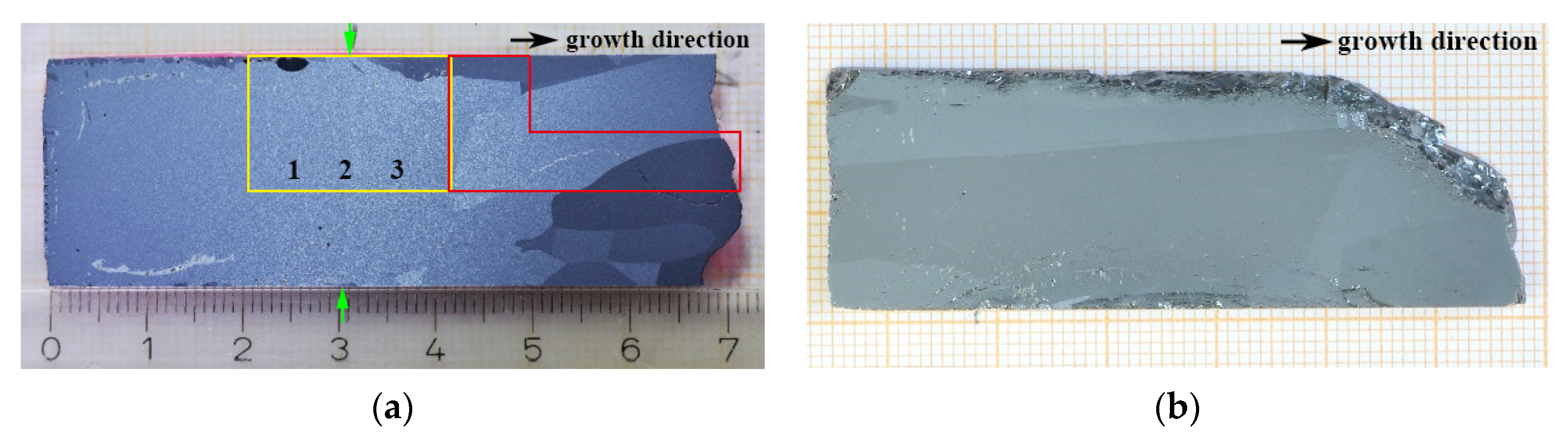
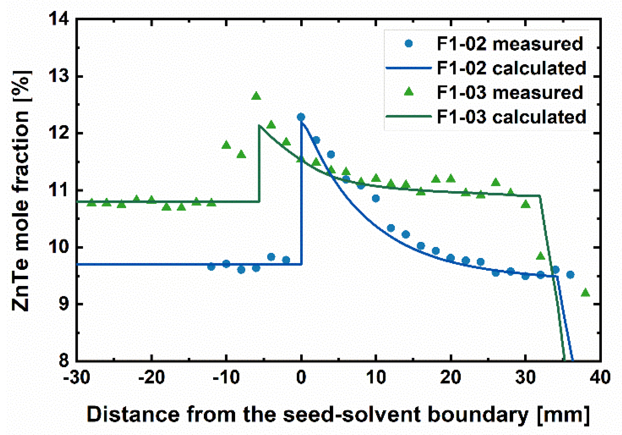
3.1. Evaluation of Compositional Uniformity

From the optical photograph of the slab F1-02 in Figure 1a, we can observe the color difference near the interface region, which is 30 mm from the seed, shown as green arrows. Under natural light, the seed and the grown crystal near the interface region present different reflections, making the interface visible to naked eyes. The original seed used in this experiment (F1-02) had a length of 31 mm. The difference of 1 mm indicates that only 1 mm of the seed was dissolved. The Laue patterns of two spots at Position 1 in the seed and Position 3 in the grown crystal (Figure 1a) demonstrate that the angels between these two area surfaces and (111) plane are 30.81° and 30.76°, respectively. This result suggests that the two grains share the same orientation, and the seeding process is successful. Figure 2a (Supplementary File S1) shows the θ–2θ scans of the 111 reflections at three spots, namely in the seed, the boundary and the grown crystal region (Position 1, 2 and 3 as shown in Figure 1a). At the interface region, shown in red color, the 111 peak is splitting, indicating the variation of the lattice parameter, which in turn reflects the variation in ZnTe mole fraction in CZT. When applying the Bragg’s law [19] and Vegard’s law [20], the ZnTe variation at the interface is calculated to be 2.4% mole fraction. Figure 2b (Supplementary File S1) illustrates the ω scans of the 111 reflections at these three spots. Boundary_1 and boundary_2 denote the seed side and the grown crystal side at the boundary, respectively. The broadening and diffuse scattering of the peaks of boundary_2 and grown crystal suggest that the crystal quality deteriorates (mosaic tilt) and more defects exist at the boundary and in the grown crystal region than in the seed.
Figure 3 (Supplementary File S2) shows the EDX results of ZnTe mole fraction as well as the calculated value from a mathematical model [21]. The results confirm that the ZnTe content variation at the interface of F1-02 is 2.51% mole fraction at about 30 mm from the seed, which is consistent with the aforementioned HRXRD result. Considering this, some parameters were adjusted for F1-03, including enhancing the CdTe content in the Te-rich solution zone from 5% to 10%, changing the temperature profile and rearranging the heater position 5 mm towards the seed side. After these adjustments, the ZnTe content variation in F1-03 is found to be reduced efficiently to about 1.02% at the interface. On the other hand, the position of the interface for F1-03 is shifted towards the seed by 7.5 mm instead of 1 mm to the seed, indicating that a larger portion of the seed was dissolved. This suggests that moving the heater position by 3 mm is expected to be sufficient for the space experiments. Furthermore, it is observed that the ZnTe concentration of both crystals decreases gradually as the growth/solidification continues and it approaches to the value of the ZnTe content in the feeds in the end of growth. The cause of the decrease is the following. The ZnTe concentration in the crystal at beginning of growth is higher than in the feed. Therefore, the amount of ZnTe outgoing from the solution into the growing crystal exceeds the ZnTe amount received from the feed. The solution is gradually depleted with ZnTe, resulting in decreasing ZnTe concentration in the growing crystal.

3.2. Structural Defects Analysis

Figure 4 displays the infrared transmission images and birefringence images of some typical defects in CZT crystals. The defects and their related local stress fields are clearly illustrated. In Figure 4a,b one grain boundary is observed, and it induces strong stress, which is revealed by the high contrast in the birefringence image. In Figure 4c,d; however, we can find several grain boundaries, which show different degrees of birefringence contrast. The twin boundary in Figure 4e,f generates a rather different stress field when compared to the grain boundaries. This suggests that the stresses associated with the wall contact are relieved due to the formation of twins. Two large inclusions can be found in Figure 4g,h, one with hexagonal or near triangular shape, and the other one with elongated rectangular shape. In the middle part some pearl string inclusions are illustrated. All of these inclusions induce strong stress fields. The Te droplet entrapment of a star-like shape corresponds in our crystals to the local stress generation at the hexagon and rectangle edges [22].
Figure 5 displays the infrared transmission images and birefringence images of F1-02 and F1-03. Clearly, from the infrared images in Figure 5a,c we find numerous large inclusions decorating in the peripheral regions of both slabs. Their sizes range from micrometers to millimeters. The origin of these large inclusions results inherently from the utilizing of Te-rich solution in THM growth and ampoule wall contact. These inclusions generate large amounts of stress around them, as revealed by the brightness contrast in the birefringence images in Figure 5b,d. Some large inclusions are observed decorating at a twin boundary (TB) in F1-03, which further generates stress in that region.
It is noteworthy that, in Figure 5b, high degrees of stress concentrate in the growth interface region (I) of F1-02. The accumulation of this stress is induced by the lattice distortion, which originates from the large ZnTe content variation at the growth interface of F1-02. In the interior of the seed, not much stress can be observed except that from several large inclusions (TI*). While in the interior of the grown crystal, three high stress fields are clearly discerned. The first one, illustrated in a red circle, is generated from an inclusion (TI**). The second and more severe one in the middle is caused by the crack (C). The last one near to the crack is located at a grain boundary (GB).
In contrast, the interior of matrix of F1-03 in Figure 5d is almost free from stress. No visible stress exists at the growth interface (I), indicating the successful reduction of ZnTe content variation at that region of F1-03. Although at the lower part of the end crystal we can observe several stress fields, which are caused by the grain boundary defects (GB1 and GB2), there are also some large inclusions (TI) and cracks (C) near the periphery. Due to wall contact and accumulation of large size inclusions in this region, stresses are generated and propagate into the interior, thereby forming cracks.
From the above results, we deduce that the CdTe content of 5% in the Te-rich zone results in larger variation of ZnTe content at the interface. The resulting ZnTe variation leads to high degree of lattice distortion and stress field at the interface, which propagates further into the interior of the grown crystal. This stress is efficiently minimized by enhancing the CdTe content from 5% to 10%.
A back reflection mapping of the interface area of F1-02 (in yellow frame in Figure 1a) is shown in Figure 6a and the corresponding infrared image of the scanned region is shown in Figure 6b. The ampoule wall and the huge inclusions (TI) are responsible for inducing excessive stress from the peripheral regions of the slabs. Scratches (Sc) on the surface appear on both sides. It is obvious that a large inclusion (TI1) in the seed generates high degrees of stress, shown as white contrast in XWBT image. Several comparatively smaller inclusions (TI2–TI4), displayed as smaller white dots, can be found in the seed. Except for the inclusions and scratches on the near surface region, the interior of the seed is almost stress free. However, high lattice distortion is observed in the growth interface region (I), which is generated mainly by the ZnTe concentration variation at the interface. This stress propagates forward into the grown crystal region, giving rise to the formation of dislocation networks (D). Additionally, many white streaks are slightly visible, and they prevail the whole grown crystal, which show a concave shape. The authors assume that these streaks originate from the inclusion striations (IS) under the influence of temperature periodic fluctuations and the resulting variation in the instantaneous growth rate [15].
In addition to Figure 6, back reflection topographs recorded from different regions of the grown crystal in F1-02 (in red frame in Figure 1a) is shown in Figure 7. The crystal area is highly distorted, indicating that this region is heavily strained. The overlapping and separation of the images arise from different senses of tilt between the neighboring grains or subgrains. It is obvious that this region exhibits a relatively higher density of dislocation density and subgrain boundaries (SB). At the upper right part, an individual grain (G1) is nucleated at the wall contact region. Again, we can observe the strain originated from the large sized inclusions near the periphery of the crystal. Another individual grain (G2) can be found at the bottom of the image. Except for a subgrain (SB2), this region is almost stress free. The middle grain shares the same orientation as the seed. The upper left region is concentrated with dislocation networks (D). A localized orientation contrast associated with distortion suggests the existence of a different grain, which is generated due to the wall contact and large inclusions in that region. The stress extends into the interior, resulting in the formation of extensive dislocation networks. Two inclusions (TI1 and TI2) shown as white dots appear at the left region. The slightly bigger inclusion (TI1) induces a high degree of stress, which is also illustrated in the birefringence image (TI**) in Figure 4b. The right region is heavily strained, which shows high consistence with the birefringence result in Figure 4b. At the regions of the crack (C) and the grain/subgrain boundaries, high degrees of stress fields are formed. High density of dislocations is generated around the crack. These dislocations realign to form tilt subgrain boundaries by the polygonization process, such as gliding and climbing [23,24]. Combining the two topographies with the birefringence result in Figure 4b, it can be easily found that the stress generated at the interface propagates into the interior region and contribute with the inclusions and grain boundaries to the formation of the crack.

3.3. Electrical Performance

Figure 8 illustrates the resistivity results of F1-02 and F1-03 from Contactless Resistivity Mapping. As shown in the figure, the resistivity over the entire areas of the two samples was found to be in the range of 0.8–9 × 10⁹ Ωcm, which is consistent with high quality CZT materials [25,26,27]. The resistivities of F1-02 and F1-03 are in the order of 3 × 10⁹ Ωcm and 1 × 10⁹ Ωcm, respectively. The content variation in ZnTe leads to a variation in the bandgap, the number of photogenerated electron-hole pairs and the leakage current in the crystal [28]. F1-03 generally has slightly higher ZnTe content than F1-02, as shown in the EDX results in Figure 3. The excessive ZnTe content regarding stoichiometry further leads to higher concentration of free carriers. Hence, the resistivity of F1-03 is lower. Several regions in both grown crystals show relatively high resistivity than other regions. It is assumed that the abundant grain boundary defects and the cracks including the associated dislocation networks are related to the increase of the resistivity. Such defects affect the charge carrier density by trapping the free carrier, which further leads to resistivity variation.

4. Discussion

In this work we investigated the extended defects, the resulting stress and resistivity of two CZT crystals grown by the THM. The aims are to understand the correlation of these observed defects and growth parameters, and to determine the parameters for the space experiments.
Extensive structural defects and strain were observed in some regions of the grown crystals. Since THM growth occurs from the Te-rich solvent zone, Te can be entrapped into the grown crystals due to microscopic irregularities, forming as a result to a high concentration of Te-rich secondary phases. These large inclusions generate extensive stresses, especially in the periphery of the crystals. In addition, wall contact between the ampoule and the CZT crystals induces shear stresses, which further lead to the formation of dislocations and slip bands propagating into the interior of the crystals. As a result, dislocations realign to form tilt subgrain boundaries at these regions.
Dislocation networks were observed at the seed interface, which propagate into the interior of the grown crystal. The stress is reduced in F1-03 when increasing the CdTe content in the Te-rich zone from 5% to 10%. This suggests that stresses can originate from the ZnTe mole fraction variation at the growth interface and the associated lattice mismatch. Furthermore, the resistivity of F1-03 is one order lower than that of F1-02 and the ZnTe mole fraction at the growth interface is slightly higher. Therefore, the defect microstructure and the electrical properties of the grown crystals are affected by the adjustment of CdTe composition in the Te-rich zone. Hence, the authors believe that 10% of CdTe in the Te-rich zone will be more beneficial for the flight experiments.
The shift of 7.5 mm of the interface position indicates that more part of the seed is dissolved in F1-03. The rearrangement of the heater position contributes to this result. Therefore, we assume that the adjustment of heater position for 3 mm would be sufficient for the space experiments.
Slight thermal stresses are observed in the grown crystals, which originate from the inclusion striations resulting from the periodic temperature variation. No dramatic change of the resistivity is caused by the striation patterns. However, the inclusions can degrade the charge carrier trapping efficiency. Methods to damp the temperature variations would be of significance.
The crystal F1-02 manifest more grain boundaries and cracks than F1-03 as the growth continues. Their formation can be attributed to the temperature gradient at the interface. Due to the heat loss through the changes in seed and feed lengths as growth continues, the temperature gradient at the interface and the growth rate tend to vary. As a result, grains and cracks can be formed to relieve stresses. Such defects affect the charge carrier density thus resulting in resistivity variation. It was reported earlier that evident charge loss was observed in the region with high concentration of dislocations [10]. Furthermore, it is revealed that grain boundary defects can play a dominant role in increasing the resistivity of CZT crystals [24]. After adjusting the temperature profile in F1-03 to reach higher consistency of the growth rate, grains and cracks are distinctly reduced.

5. Conclusions

In this work the compositional homogeneity, structural defects and resistivity of two CZT crystals grown by the THM from ground experiments were investigated. As expected, large inclusions near the periphery can generate high degree of strain fields, comprising the formation of dislocation slip bands and subgrain boundaries. From the HRXRD and EDX results we observed a ZnTe content variation at the seed/grown crystal interface. According to the birefringence images and back reflection topographs, this ZnTe variation induces severe local stress associated with extensive deformation microstructures in that region, especially dislocation networks, which propagates forward into the grown crystal. By increasing the CdTe composition from 5% to 10% in the Te-rich solution zone and adjusting the heater position, the ZnTe content variation in F1-03 and the resulting stress are efficiently reduced. Additionally, a heavily strained region with grain boundaries and cracks in F1-02 is illustrated and believed to be relative to thermal gradient at the growth interface. These dominant defects further result in the variation of the bulk resistivity in the crystals. The as-grown crystals exhibit a high bulk resistivity, which ranges from 109 Ωcm to 1010 Ωcm.

Supplementary Materials

The following are available online at https://0-www-mdpi-com.brum.beds.ac.uk/article/10.3390/cryst11111402/s1, File S1: HRXRD θ-2θ scan and ω scan of F1-02; File S2: EDX results of ZnTe content distributions along the growth direction.

Author Contributions

Conceptualization, M.F. and A.S.S.; methodology, J.Z., A.F. and A.S.S.; software, A.S.S.; validation, A.F., A.S.S. and M.F.; formal analysis, J.Z.; investigation, J.Z., A.F., N.N.K., L.K., M.P.K.; resources, M.F. and A.S.S.; data curation, J.Z.; writing—original draft preparation, J.Z.; writing—review and editing, A.F., A.S.S., N.N.K., L.K., M.P.K., E.H., A.C. and M.F.; visualization, J.Z., A.S.S. and M.F.; supervision, M.F.; project administration, M.F.; funding acquisition, M.F. All authors have read and agreed to the published version of the manuscript.

Funding

This research was supported and funded by the German Aerospace Center (DLR) under Nr. 2100117701.

Data Availability Statement

The data presented in this study are available in the Supplementary Materials.

Acknowledgments

This work was partially carried out within the BIRD collaboration between University of Freiburg and KIT. We thank the Karlsruhe Research Accelerator and the KIT synchrotron light source for the provision of beam time. The authors would like to thank Andreas N. Danilewsky from Crystallography Institute of Freiburg for providing the X-ray films for XWBT measurements, and Manfred Kranz-Probst for the preparation of the ampoules. We thank Yun Wang and two reviewers for helpful comments on the manuscript.

Conflicts of Interest

The authors declare no conflict of interest.

References

  1. Yang, G.; James, R.B. (Eds.) Chapter IIC—Applications of CdTe, CdZnTe, and CdMnTe Radiation Detectors. In CdTe and Related Compounds; Physics, Defects, Hetero- and Nano-Structures, Crystal Growth, Surfaces and Applications; European Materials Research Society Series; Elsevier: Amsterdam, The Netherlands, 2010; pp. 145–225. ISBN 978-0-08-096513-0. [Google Scholar]
  2. Zhou, B.; Jie, W.; Wang, T.; Yin, L.; Yang, F.; Zhang, B.; Xi, S.; Dong, J. Modification of Growth Interface of CdZnTe Crystals in THM Process by ACRT. J. Cryst. Growth 2018, 483, 281–284. [Google Scholar] [CrossRef]
  3. Chen, H.; Li, H.; Reed, M.D.; Sundaram, A.G.; Eger, J.; Hugg, J.W.; Abbaszadeh, S.; Li, M.; Montemont, G.; Verger, L.; et al. Development of Large-Volume High-Performance Monolithic CZT Radiation Detector. In Proceedings of the Hard X-Ray, Gamma-Ray, and Neutron Detector Physics XX, International Society for Optics and Photonics, San Diego, CA, USA, 1 January 2018; Volume 10762, p. 107620N. [Google Scholar]
  4. Roy, U.N.; Burger, A.; James, R.B. Growth of CdZnTe Crystals by the Traveling Heater Method. J. Cryst. Growth 2013, 379, 57–62. [Google Scholar] [CrossRef]
  5. Shiraki, H.; Funaki, M.; Ando, Y.; Tachibana, A.; Kominami, S.; Ohno, R. THM Growth and Characterization of 100 mm Diameter CdTe Single Crystals. IEEE Trans. Nuclear Sci. 2009, 56, 1717–1723. [Google Scholar] [CrossRef]
  6. Chung, H.; Raghothamachar, B.; Dudley, M.; Larson, D.J., Jr. Synchrotron White Beam X-Ray Topography Characterization of Structural Defects in Microgravity and Ground-Based CdZnTe Crystals. In Proceedings of the Space Processing of Materials, International Society for Optics and Photonics, Denver, CO, USA, 12 July 1996; Volume 2809, pp. 45–56. [Google Scholar]
  7. Hossain, A.; Bolotnikov, A.E.; Camarda, G.S.; Cui, Y.; Gul, R.; Roy, U.N.; Yang, G.; James, R.B. Direct Observation of Influence of Secondary-Phase Defects on CZT Detector Response. J. Cryst. Growth 2017, 470, 99–103. [Google Scholar] [CrossRef] [Green Version]
  8. Buis, C.; Marrakchi, G.; Lafford, T.A.; Brambilla, A.; Verger, L.; Gros d’Aillon, E. Effects of Dislocation Walls on Image Quality When Using Cadmium Telluride X-Ray Detectors. IEEE Trans. Nuclear Sci. 2013, 60, 199–203. [Google Scholar] [CrossRef]
  9. Bolotnikov, A.E.; Babalola, S.; Camarda, G.S.; Cui, Y.; Gul, R.; Egarievwe, S.U.; Fochuk, P.M.; Fuerstnau, M.; Horace, J.; Hossain, A.; et al. Correlations Between Crystal Defects and Performance of CdZnTe Detectors. IEEE Trans. Nuclear Sci. 2011, 58, 1972–1980. [Google Scholar] [CrossRef]
  10. Bolotnikov, A.E.; Babalola, S.O.; Camarda, G.S.; Chen, H.; Awadalla, S.; Cui, Y.; Egarievwe, S.U.; Fochuk, P.M.; Hawrami, R.; Hossain, A.; et al. Extended Defects in CdZnTe Radiation Detectors. IEEE Trans. Nuclear Sci. 2009, 56, 1775–1783. [Google Scholar] [CrossRef]
  11. Camarda, G.S.; Andreini, K.W.; Bolotnikov, A.E.; Cui, Y.; Hossain, A.; Gul, R.; Kim, K.-H.; Marchini, L.; Xu, L.; Yang, G.; et al. Effect of Extended Defects in Planar and Pixelated CdZnTe Detectors. Nuclear Instrum. Methods Phys. Res. Sect. A Accel. Spectrometers Detect. Assoc. Equip. 2011, 652, 170–173. [Google Scholar] [CrossRef]
  12. Benz, K.-W.; Fiederle, M. (Eds.) Chapter IC—Crystal Growth of CdTe/CdZnTe in Microgravity. In CdTe and Related Compounds; Physics, Defects, Hetero- and Nano-Structures, Crystal Growth, Surfaces and Applications; European Materials Research Society Series; Elsevier: Amsterdam, The Netherlands, 2010; pp. 1–144. ISBN 978-0-08-096513-0. [Google Scholar]
  13. Borisenko, E.B.; Kolesnikov, N.N.; Senchenkov, A.S.; Fiederle, M. Crystal Growth of Cd1−xZnxTe by the Traveling Heater Method in Microgravity on Board of Foton-M4 Spacecraft. J. Cryst. Growth 2017, 457, 262–264. [Google Scholar] [CrossRef]
  14. Benz, K.W.; Dold, P. Crystal Growth under Microgravity: Present Results and Future Prospects towards the International Space Station. J. Cryst. Growth 2002, 237–239, 1638–1645. [Google Scholar] [CrossRef]
  15. Zou, J.; Fauler, A.; Senchenkov, A.S.; Kolesnikov, N.N.; Fiederle, M. Analysis of Te Inclusion Striations in (Cd,Zn)Te Crystals Grown by Traveling Heater Method. Crystals 2021, 11, 649. [Google Scholar] [CrossRef]
  16. Tobin, S.P.; Tower, J.P.; Norton, P.W.; Chandler-Horowitz, D.; Amirtharaj, P.M.; Lopes, V.C.; Duncan, W.M.; Syllaios, A.J.; Ard, C.K.; Giles, N.C.; et al. A Comparison of Techniques for Nondestructive Composition Measurements in CdZnTe Substrates. JEM 1995, 24, 697–705. [Google Scholar] [CrossRef]
  17. Rack, A.; Weitkamp, T.; Bauer Trabelsi, S.; Modregger, P.; Cecilia, A.; dos Santos Rolo, T.; Rack, T.; Haas, D.; Simon, R.; Heldele, R.; et al. The Micro-Imaging Station of the TopoTomo Beamline at the ANKA Synchrotron Light Source. Nucl. Instrum. Methods Phys. Res. Sect. B Beam Interact. Mater. At. 2009, 267, 1978–1988. [Google Scholar] [CrossRef]
  18. Danilewsky, A.N.; Simon, R.; Fauler, A.; Fiederle, M.; Benz, K.W. White Beam X-Ray Topography at the Synchrotron Light Source ANKA, Research Centre Karlsruhe. Nucl. Instrum. Methods Phys. Res. Sect. B: Beam Interact. Mater. Atoms. 2003, 199, 71–74. [Google Scholar] [CrossRef]
  19. Bragg, W.H.; Bragg, W.L. The Reflection of X-Rays by Crystals. Proc. R. Soc. Lond. Ser. A 1913, 88, 428–438. [Google Scholar] [CrossRef]
  20. Vegard, L. Die Konstitution der Mischkristalle und die Raumfüllung der Atome. Z. Phys. 1921, 5, 17–26. [Google Scholar] [CrossRef]
  21. Senchenkov, A.S.; Fiederle, M.; Kolesnikov, N.N. CZT Crystal Growth by THM in Microgravity—Preparation of Experiments for FOTON-M4 Mission. In Proceedings of the the IAC Proceedings 2014, Toronto, ON, Canada, 29 September–3 October 2014; Volume IAC-14-A2.4.7. [Google Scholar]
  22. Laasch, M.; Kloess, G.; Kunz, T.; Schwarz, R.; Grasza, K.; Eiche, C.; Benz, K.W. Stress Birefringence in Vapour-Grown CdTe and Its Correlation to the Growth Techniques. J. Cryst. Growth 1996, 161, 34–39. [Google Scholar] [CrossRef]
  23. Durose, K.; Russell, G.J. Structural Defects in CdTe Crystals Grown by Two Different Vapour Phase Techniques. J. Cryst. Growth 1988, 86, 471–476. [Google Scholar] [CrossRef]
  24. Chung, H.; Raghothamachar, B.; Wu, J.; Dudley, M.; Larson, D.J.; Gillies, D.C. Characterization of Growth Defects in CdZnTe Single Crystals by Synchrotron White Beam X-Ray Topography. MRS Online Proc. Libr. Arch. 1995, 378. [Google Scholar] [CrossRef]
  25. Zázvorka, J.; Pekárek, J.; Grill, R.; Belas, E.; Ridzoňová, K.; Pipek, J.; Franc, J. Inhomogeneous Resistivity and Its Effect on CdZnTe-Based Radiation Detectors Operating at High Radiation Fluxes. J. Phys. D: Appl. Phys. 2019, 52, 325109. [Google Scholar] [CrossRef]
  26. Zázvorka, J.; Franc, J.; Hlídek, P.; Grill, R. Photoluminescence Spectroscopy of Semi-Insulating CdZnTe and Its Correlation to Resistivity and Photoconductivity. J. Lumin. 2013, 143, 382–387. [Google Scholar] [CrossRef]
  27. Kim, K.H.; Na, Y.H.; Park, Y.J.; Jung, T.R.; Kim, S.U.; Hong, J.K. Characterization of High-Resistivity Poly-CdZnTe Thick Films Grown by Thermal Evaporation Method. IEEE Trans. Nuclear Sci. 2004, 51, 3094–3097. [Google Scholar] [CrossRef]
  28. James, R.B.; Schlesinger, T.E.; Lund, J.; Schieber, M. Chapter 9 Cd1−xZnxTe Spectrometers for Gamma and X-Ray Applications. In Semiconductors and Semimetals; Elsevier: Amsterdam, The Netherlands, 1995; Volume 43, pp. 335–381. ISBN 978-0-12-752143-5. [Google Scholar]
Figure 1. Optical photograph of the slabs cut along the ingot axis: (a) F1-02; (b) F1-03 [14]. We performed XRD measurements at Position 1, 2, 3 and XWBT in the areas in yellow and red frames.
Crystals 11 01402 g001
Figure 2. HRXRD θ-2θ scan (a) and ω scan (b) at the three positions of F1-02. The splitting of the peak at the boundary and the shifting of the peak position in the grown crystal from the θ-2θ scans indicate the variation in lattice parameter. The broadening and diffuse scattering of the peaks from the ω scans suggest the existence of more defects in the grown crystal region.
Crystals 11 01402 g002
Figure 3. ZnTe content distributions along the growth direction of the crystals and calculated value from mathematical simulation [21]. ZnTe content variation at the interface of F1-02 is higher than that in F1-03. In both crystals, gradual reductions in the ZnTe content are observed as the growth/solidification continues.
Crystals 11 01402 g003
Figure 4. Infrared transmission images and birefringence images showing related local stress fields of typical defects observed in our CZT crystals: grain boundaries (ad); a twin boundary (e) and (f); Te inclusions (g) and (h).
Crystals 11 01402 g004
Figure 5. Infrared transmission images and birefringence images of F1-02 (a) and (b) and F1-03 (c) and (d). Abundant large sized inclusions in the peripheral regions of both slabs generate high degree of stress filed. An evident reduction of stress generated at the interface (I) of F1-03 was observed when compared to F1-02. Most of the stress originates from twin boundary (TB), inclusions (TI), grain boundaries (GB) and cracks (C).
Crystals 11 01402 g005
Figure 6. XWBT back reflection mapping (a) and infrared image (b) near the interface region of F1-02. Some scratches (Sc) exist on the surface. The observation of white dots suggests the stress induced by Te inclusions (TI1–TI4). Extensive distortion and dislocation networks (D) accumulate at the interface and further extend into the grown crystal region. White streaks prevail the grown crystal, which are considered to be caused by the inclusion striations (IS) [15].
Crystals 11 01402 g006
Figure 7. Back reflection topographs recorded from the grown crystal region of F1-02 showing extensive defect structures. Two individual grains (G1 and G2) are observed. High density of dislocation network (D) and subgrain boundaries (SB) are generated near the periphery and around the crack (C).
Crystals 11 01402 g007
Figure 8. Contactless resistivity mapping of: (a) F1-02 and (b) F1-03.
Crystals 11 01402 g008
Publisher’s Note: MDPI stays neutral with regard to jurisdictional claims in published maps and institutional affiliations.

