
Survey of Mura Defect Detection in Liquid Crystal Displays Based on Machine Vision
by
 ,
,
Wuyi Ming
1, 
Shengfei Zhang
1,
Xuewen Liu
2,*,
Kun Liu
1,
Jie Yuan
1,
Zhuobin Xie
1,3,
Peiyan Sun
1 and
Xudong Guo
1 1
Henan Key Laboratory of Intelligent Manufacturing of Mechanical Equipment, Zhengzhou University of Light Industry, Zhengzhou 450002, China
2
School of Vehicle and Automation, Guangzhou Huaxia Vocational College, Guangzhou 510900, China
3
Guangdong Provincial Key Laboratory of Digital Manufacturing Equipment, Guangdong HUST Industrial Technology Research Institute, Dongguan 523808, China
*
Author to whom correspondence should be addressed.
Crystals 2021, 11(12), 1444; https://0-doi-org.brum.beds.ac.uk/10.3390/cryst11121444
Submission received: 19 October 2021
/
Revised: 9 November 2021
/
Accepted: 19 November 2021
/
Published: 24 November 2021
(This article belongs to the Special Issue Liquid Crystals in China)
Abstract
:Liquid crystal display (LCD) is a display device based on liquid crystal electro-optic effect, and LCDs have gradually appeared and have become an indispensable part of people’s lives. In the development of LCD technology, the detection of Mura defects is a key concern in the manufacturing process. The Mura defect is a kind of display defect with low contrast and an irregular shape. This study first explains the mechanism of Mura defects in the LCD manufacturing process and classifies typical Mura defects. Then, three main purposes for the defect detection of LCDs are compared, and the advantages and disadvantages are conducted. Following that, this research examines reviews the linked literature on image preprocessing, feature extraction, dimension reduction, and classifiers of Mura defects. Finally, the future development trend and research direction of Mura defect detection based on machine vision can be drawn by this study.
1. Introduction
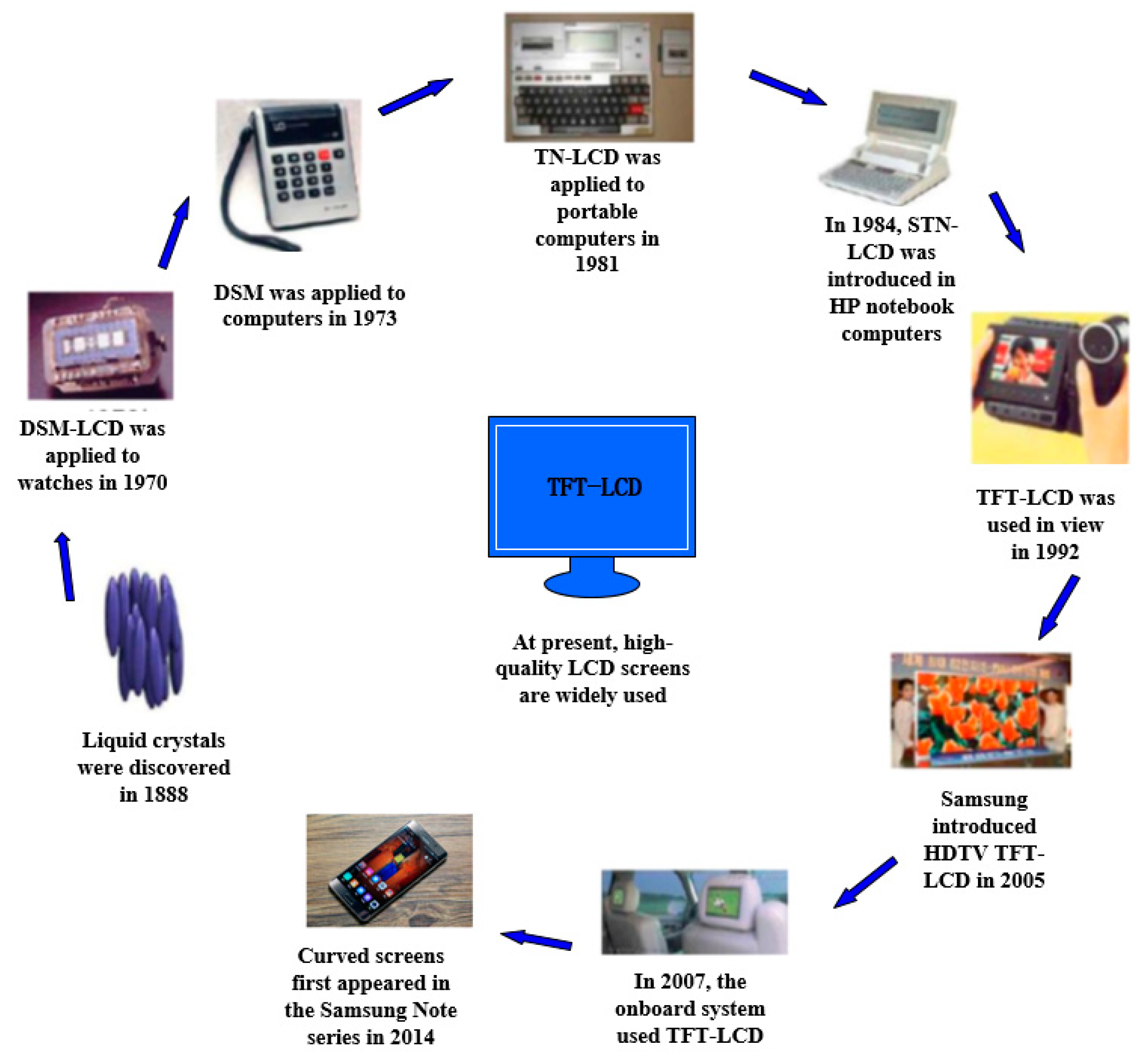
After mankind entered the information age, the hardware carriers of information played an important role in the dissemination of information. As the primary hardware carrier of information, display devices play an increasingly important role in many fields [1], such as computers, mobile phones, commerce, medical treatment, machinery, aerospace, etc. In recent decades, great changes have taken place in the display industry. Liquid crystal displays (LCD) have gradually appeared and have grown up to be an indispensable part of people’s lives. Figure 1 shows the development process of liquid crystal display technology, from the earliest principle to the current universal application. In the first stage, liquid crystal was discovered in 1888 and the first liquid crystal display was taken in the United States in 1968. It was after 1970–1972 that human beings applied LCD to watches. In the second stage, from 1971 to 1984, Switzerland produced TN-LCD (twisted nematic) liquid crystal display. The third stage was from 1984 to 1990, during which Japan mastered STN-LCD and TFT-LCD production technology. The fourth stage is from 1990 to 1995, and LCD can display high-quality color images. At the beginning of the fifth stage, China has paid more attention to the LCD industry and invested heavily in the research of LCD displays. Most notably, in June 2003, BOE announced that it would invest 1.2 billion US dollars in building the fifth generation TFT-LCD production line in the Beijing zone. At present, all kinds of high-quality LCD screens are everywhere around us.
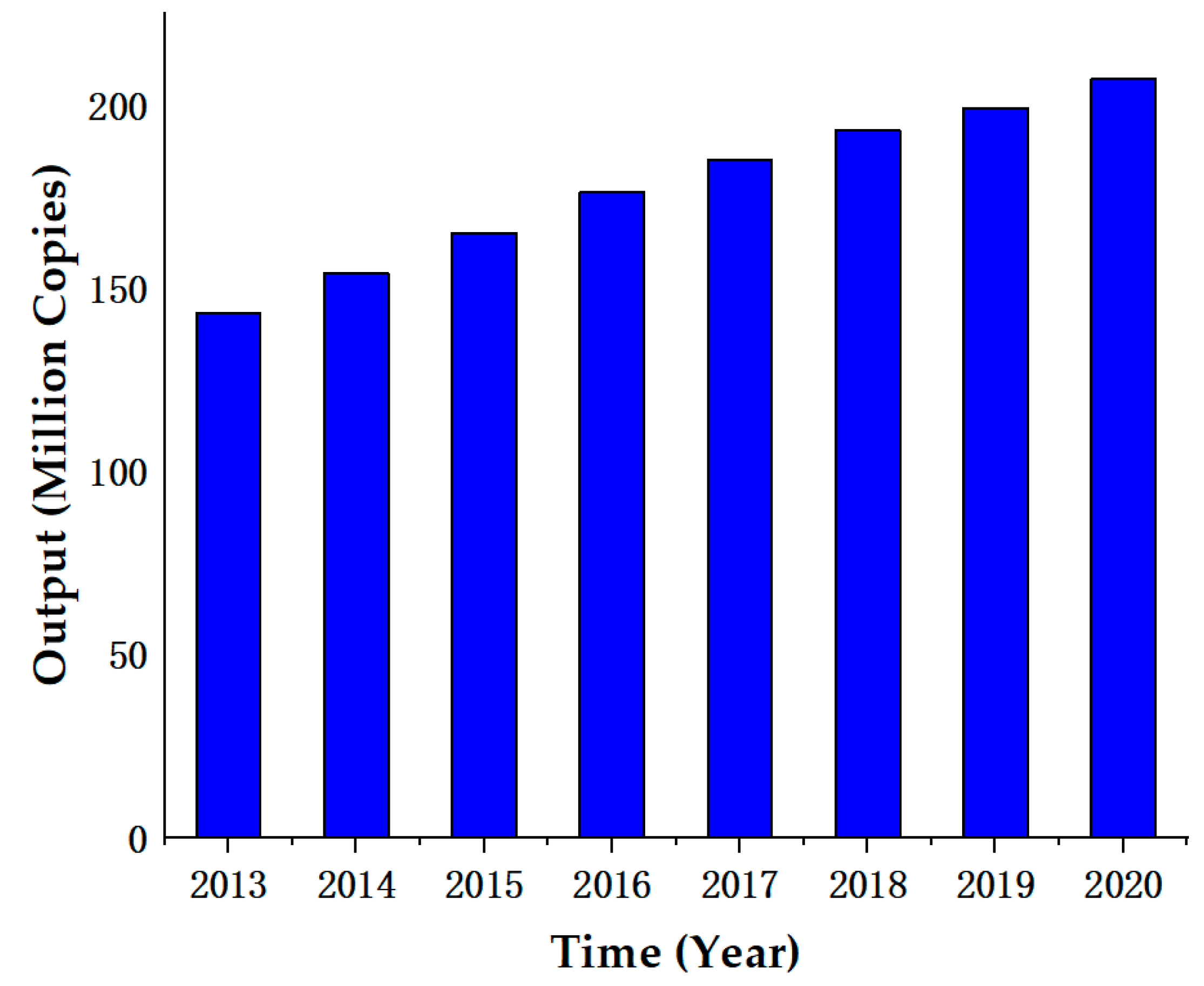
As a type of LCD, TFT-LCD has the characteristics of small size, low power consumption, high definition, small geometric distortion, large visible area, and low radiation. In recent years, it is commonly used in TVs, personal computers, smartphones, digital cameras, smartwatches, and display terminal devices [2]. From the discovery of TFT-LCD today, the global demand for TFT-LCD panels has been on an upward trend year by year [3], as shown in Figure 2.
To respond to market demands, LCDs have become larger and larger, with higher resolution and thinner thickness. However, the probability of Mura defects in LCDs is also increasing. As a result, detecting Mura defects is a difficult task, as evidenced by (1) Mura defects typically appear in localized areas with low contrast and uneven brightness [4]. Therefore, the recognition of Mura defects is extremely difficult, especially under the conditions of changing illumination [5]; (2) There is no fixed size and regular shape of Mura defects, so the same kind of Mura defects may show great differences, while different types of defects may show small differences, so it is very easy to cause misclassification of categories; (3) Samples for some Mura faults are quite uncommon. This phenomenon will cause a serious imbalance in the sample data in the recognition system, thus increasing the difficulty of identifying Mura defects. However, with the progress of technology, machine vision technology has the advantages of high efficiency, high precision, and non-contact detection, which attract more and more attention of scholars and are gradually applied to various fields. As a result, using machine vision technology to detect Mura defects is becoming increasingly popular in the industry.
Therefore, this study investigates the Mura defect detection in LCDs based on machine vision. First, this study explains the mechanism of Mura defects in the LCD manufacturing process and classifies typical Mura defects. Second, three main purposes for the defect detection of TFT-LCD screens are compared, and the advantages and disadvantages are conducted. Third, this study also reviews the related literature on image preprocessing, feature extraction, dimension reduction, and classifiers of Mura defects. Finally, the future development trend and research direction of Mura defect detection based on machine vision can be drawn by this study.
2. General Classification of Mura Defects
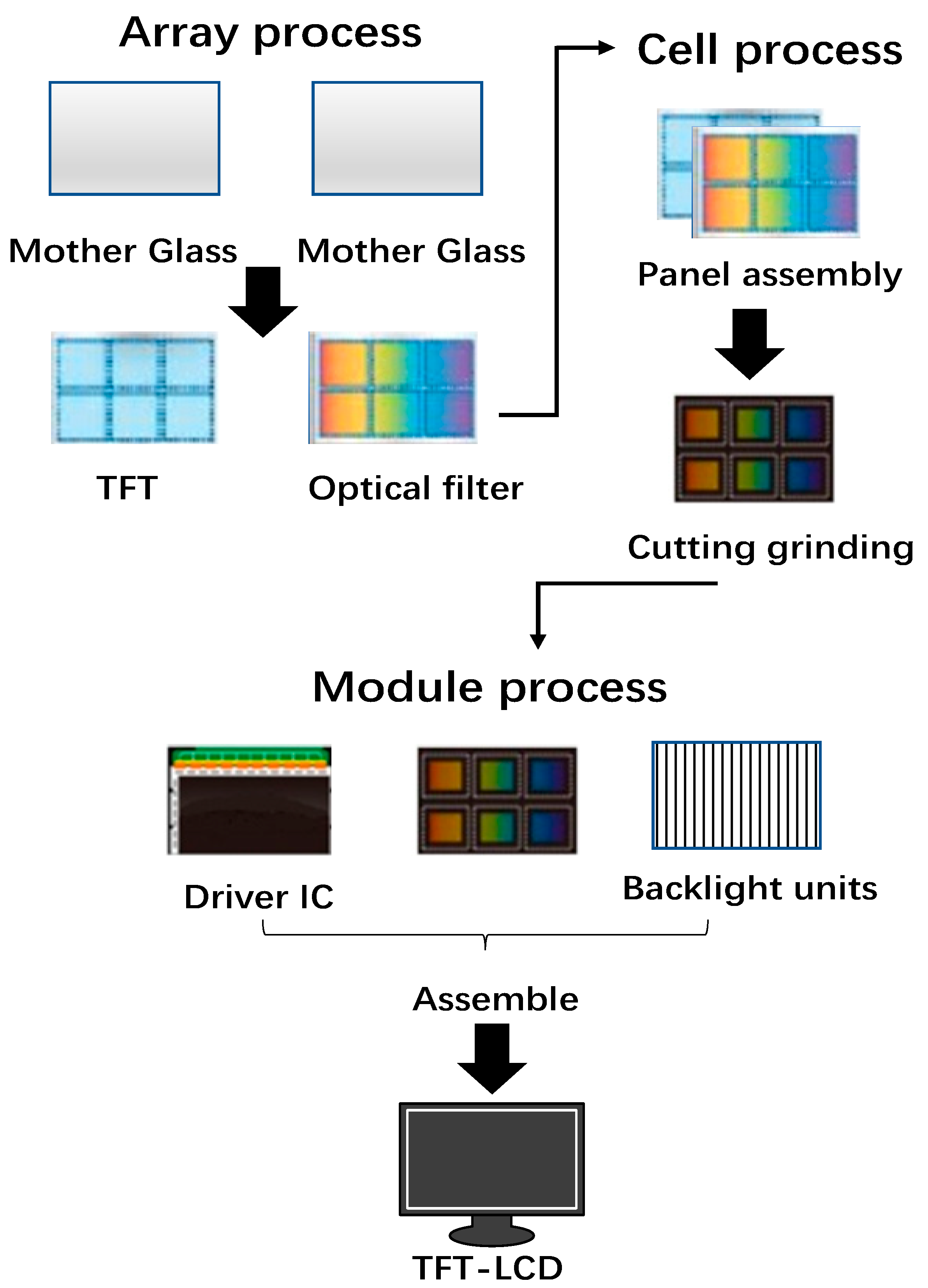
The manufacturing process of TFT-LCD is already, and the production process has strict environmental requirements. Minor flaws in the production process may cause irreparable quality problems in the finished LCD panel, which will affect the product’s visual effect and the user experience. As shown in Figure 3, the TFT-LCD manufacturing process is generally divided into three stages: the front-end array process, the middle-end cell process, and the back-end module process [6]. The array-level technology is primarily used to etch thin-film transistors on a glass substrate by etching, and then used for pixel control. The cell stage mainly completes the liquid crystal perfusion and the color filter lamination. The module stage mainly completes the assembly of the circuit and the peripheral components of the backlight board. As shown in Table 1, each stage has different Mura defects, which are the cause of some Mura defects in the three processes.
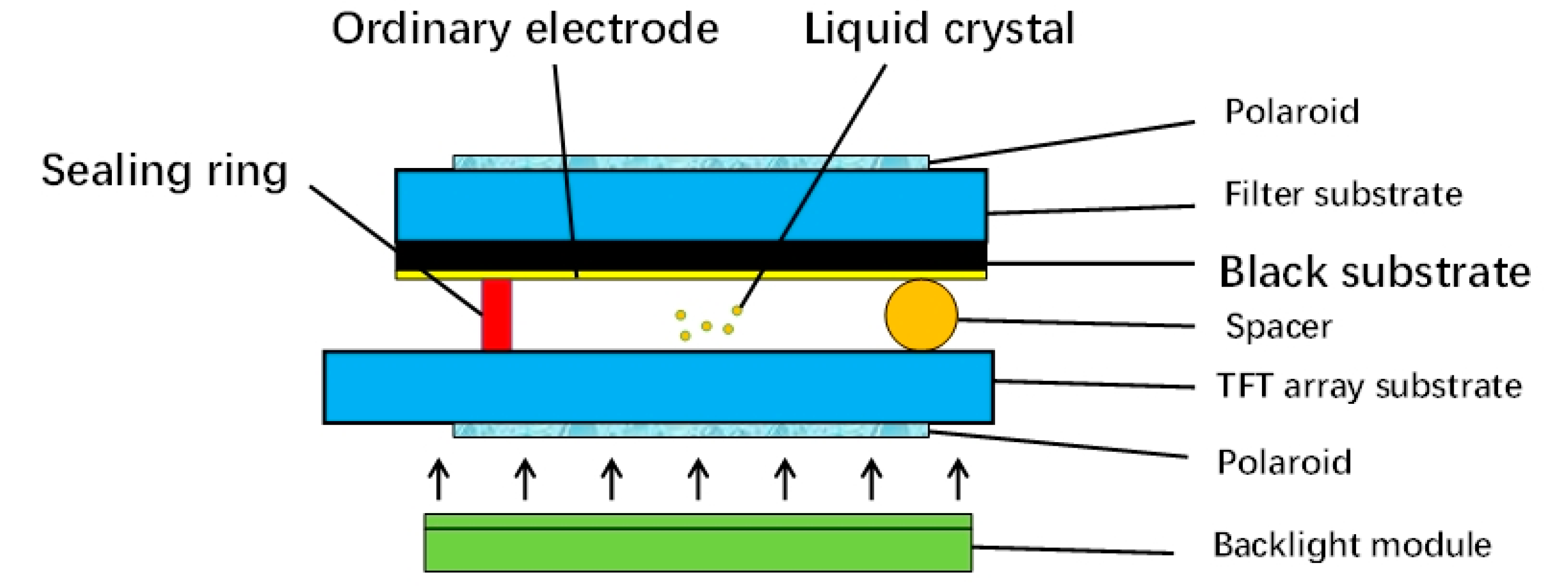
The composition of TFT-LCD is very complex, as shown in Figure 4. Generally, the liquid crystal panel mainly refers to the color filter substrate, TFT glass substrate, and the liquid crystal sandwiched between them, shown in Figure 1. In the TFT-LCD manufacturing process, there are many processes, and its production process has extremely harsh requirements on the environment. Small defects in the production process may lead to irreparable quality problems of the finished LCD panel, thus affecting the visual effect and user experience of the product. Mura defects of TFT-LCD mainly occur in three process stages: array process, cell process, and module process. The cell process is the process of assembling TFT substrate and color filter substrate and injecting liquid crystal. If the applied pressure is too large during substrate bonding, it is easy to break the pad, thus damaging the orientation layer and affecting the image. Also, if the temperature is not set properly in the bonding process, it is easy to cause uneven substrate thickness due to the temperature difference between cold and hot, thus affecting the picture uniformity. Moreover, if the bonding is not firm or misplaced, it may cause defects such as liquid crystal leakage. Finally, if air or other gases are mixed into the liquid crystal material, it is easy to cause defects such as bubbles in the liquid crystal layer. Mura defects also include uneven material characteristics of filter substrate, anisotropy of polarizer, spatial distribution and concentration difference of liquid crystal material, short circuit and open circuit of the scanning line, different local characteristics of TFT array substrate, defects of TFT unit, impurities in liquid crystal, etc.
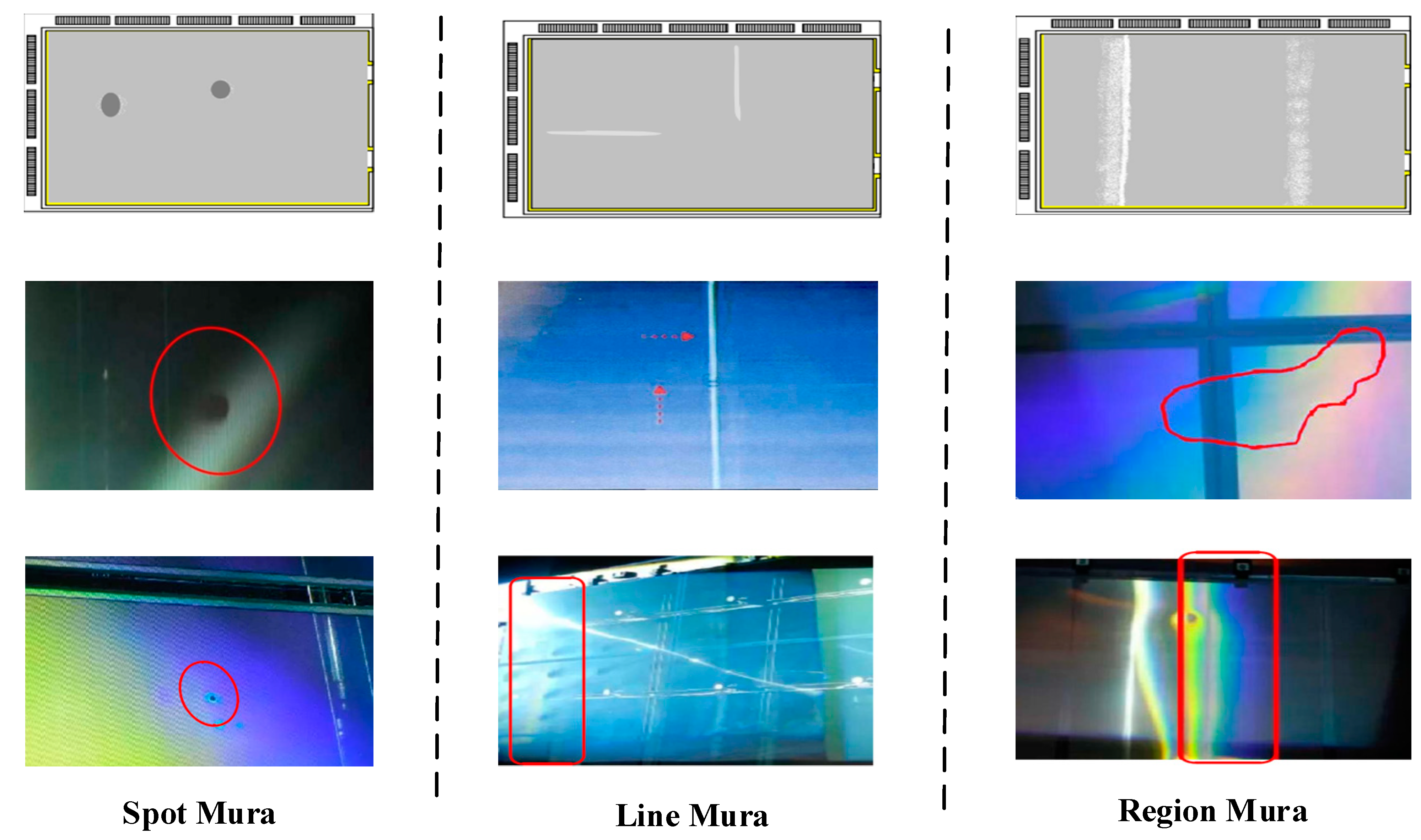
Mura defects usually appear as blocky uneven brightness, irregular shapes, low contrast, and most defects have no rules to follow. We commonly split the common Mura faults into three groups [9,10] based on the TFT-LCD driving theory and experience in the production process: spot Mura, line Mura, and region Mura. In manual inspection, filters are often used to filter light. Therefore, the performance of the filter and the degree of observation by the human eye will directly affect the judgment of Mura defects. The main factors for traditional detection methods to distinguish and classify Mura defects are the space size, average brightness, area, the center of gravity position, and shape parameter [9,11] of the Mura defect. The schematic diagram of common Mura defects is shown in Figure 5 [3].
3. Common Detection Methods for Mura Defects
There are three main purposes for the defect detection of TFT-LCD screens. First, it is utilized in the statistical analysis of defects to find out the common defects and their causes, and to analyze the weak links in the design and manufacturing process, to optimize the structural design and manufacturing process. Second, it is utilized to repair defects. Third, it is to eliminate the unqualified products to avoid the waste of the driving circuit caused by the unqualified TFT-LCD screen connected with the driving circuit. With the development of technology in China, related research on TFT-LCD has been greatly improved, laying a reliable foundation for the defect detection of Mura in TFT-LCD [12]. At present, there are three commonly used Mura defect detection methods, namely the manual detection method, the electrical measurement method, and the optical detection method based on machine vision.
The manual detection method refers to the judgment of the defect category by the experienced defect detection engineer comparing the defect sample library [3]. This is a traditional method of manually identifying Mura defects. Electrical measurement methods are usually used to detect point Mura defects and linear Mura defects caused by electrical defects such as short circuits, open circuits, poor contact, open circuit of a grid line in a panel, etc. Commonly used electrical measurement methods include the admittance circuit detection method, full-screen illumination method, probe scanning method, charge readout method, voltage image method, and electron beam scanning pixel electrode method [13]. An electrical measurement method can identify those point defects and line defects caused by electrical defects. However, electrical measurement methods are powerless to detect Mura defects caused by non-electrical reasons such as chemical pollution [14]. This requires further detection methods, such as optical measurement methods based on machine vision. The optical measurement method based on machine vision is a non-contact measurement, which uses image acquisition equipment to acquire the information displayed on the screen and perform quantitative analysis on it to determine the location and type of the defect. With the development of machine vision, the research of optical measurement has been continuously applied in different fields. For example, methods adopted and widely promoted by international standards include the spatial correlation method [15], Mura look detection algorithm [5], minimum identifiability theory [16], and so on.
Among the three detection methods of Mura defects, manual detection method, electrical measurement method, and optical measurement method based on machine vision, they have their advantages and disadvantages, as shown in Table 2.
The manual detection method [12] is to judge whether the LCD screen has Mura defects by inspecting the LCD screen one by one. Its advantage is the fact that it has better flexibility and can be well adapted to different types and different sizes of display panels. However, artificial visual recognition (manual inspection method) also has many unacceptable shortcomings, such as low detection efficiency, great subjectivity, and relatively easy to be affected by external factors.
The electrical measurement method [13] shows many advantages in a large number of applications, which can meet certain efficiency requirements, but there are also considerable limitations. This method can effectively detect point defects and line defects caused by electricity, and has some weakness for various Mura defects caused by other factors. Moreover, the electrical measurement method cannot determine the precise location and type of the defect, and it is time-consuming.
The optical measurement method based on machine vision [5,15,16] is the most ideal method for Mura defect detection and the most common method. It has a lot of advantages, which can reduce the labor cost of liquid crystal display Mura defect detection. It can also find and identify a variety of Mura defects without the conditional restrictions of electrical measurement methods. In addition, it can eliminate many shortcomings of manual detection, has high detection efficiency, high detection accuracy, and is a non-contact detection method. However, the optical measurement method also has some shortcomings. Generally, the cost of the detection equipment required by the detection method is relatively high, and it requires trained professionals to operate.
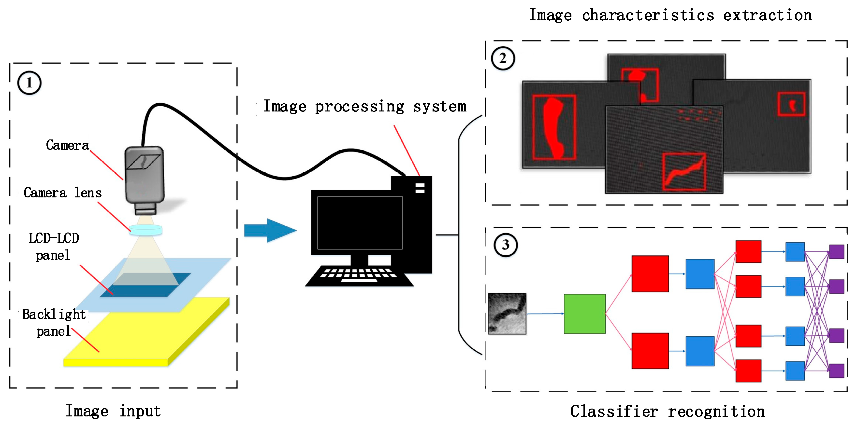
Through comparison, we can conclude that the manual detection method has the most shortcomings, and the optical measurement method based on machine vision has the most advantages. Therefore, the optical measurement method based on machine vision is the most ideal detection method. It is appropriate for many companies to detect LCD screens. It is further the trend of the development of the industry today. The flow chart of automatic optical inspection of conventional TFT-LCD Mura defects is shown in Figure 6 [3]. The image is collected through module ①, and the collected pictures are transmitted to the image processing system. Then, the image processing system performs the corresponding image processing. Image preprocessing operations include image denoising, image enhancement, suppression of image repetitive background textures, and so on. After this series of processing, the image will be sent to module ② for image positioning, dimension reduction, and image feature extraction. After determining the existing area of the defect, it can be sent to the module ③ for classifier comparison and recognition, thus completing the automatic optical inspection flow of the image’s Mura defect.
4. Image Processing for Mura Defects
In the process of acquiring the image, it can be affected by numerous factors. For example, the light intensity changes of the lighting equipment, the performance of the image acquisition equipment itself, and the proficiency of the staff in acquiring images, and so on. The quality of the original image obtained initially may be unsatisfactory. In order not to affect subsequent processing such as image analysis and image understanding, some preprocessing must be made on the acquired images [17]. Being aimed at the preprocessing method of Mura defect, this study mainly reviews image filtering and image correction.
4.1. Image Filtering
Regardless of how image acquisition, in the process of digital image collection and transmission, there is always interference from various factors, so that the acquired image is inevitably contaminated by noise, resulting in degradation of image quality. Whether the noise can be effectively removed directly affects the smooth progress of subsequent processing such as image feature extraction and classification, so appropriate methods must be taken to denoise the image. There are many ways to eliminate noise, and which one is utilized depends on the type of noise. According to the viewpoint of statistical theory, image noise can be divided into two categories: stationary and non-stationary noise. The statistical properties of noise are expressed in terms of mean, variance, correlation functions, and so on [18].
TFT-LCD panel images generally have four types of noise. (1) The TFT-LCD panel’s noise. This type of noise mainly comes from the cold cathode fluorescent lamp backlight (CCFL) as the lighting source, and the LCD screen will show periodic brightness changes [19]. (2) The electronic noise that is inherent in CCD cameras. During the working process of the camera, CCD charge injection, charge change, and output transfer charge will cause various high-frequency noises. (3) The quantization noise of digitized images. Accompanied by quantization noise generated in the image acquisition process. It reflects the difference between the digital image and the original image. (4) Additional noise. Including temperature changes, noise caused by the external environment, various dark current noises, and so on.
Image filtering [20,21,22,23] is a very active subject in the field of image processing and has been followed in many fields. The conventional methods of TFT-LCD screen image filtering include the spatial domain method and the frequency domain method. Spatial domain filtering is accomplished by template convolution in the image space with the help of templates. Frequency domain filtering is tantamount to transforming the image into frequency domain space, then multiplying it with the transfer function, and finally performing the inverse transformation [24]. For image denoising methods in Mura defect [25], there are mean filtering [26], median filtering [27], and Gaussian filtering [28]. The image effect after Gaussian filtering is the smoothest, the blur generated after median filtering is less, and the denoising effect is slightly weaker. Mean filtering will cause more loss of image details. The template coefficient of Gaussian filtering decreases with the increase of the distance from the center, and the influence of distant points on the target point is low, and the details will be preserved [29]. Therefore, it is necessary in order to choose different methods according to the desired image effect.
4.2. Image Correction
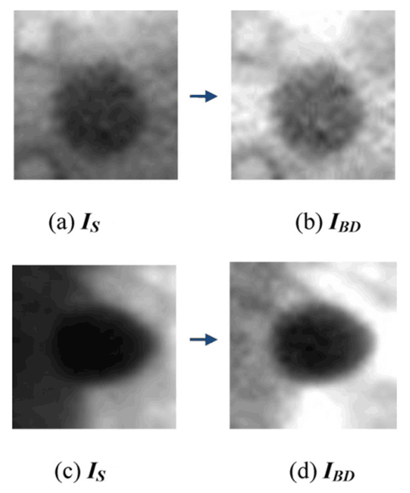
Mura defect is a defect of uneven brightness and low contrast. Since the overall brightness of the image is uneven, even if it is not obvious, it can easily be confused with the Mura defect. This has a great interference with the detection of Mura defects. If the contrast of the defect is minimal, the overall brightness unevenness is relatively obvious, which can easily cause false detection and misjudgment of the defect. So, the correction of image brightness is very important for Mura defect detection. Figure 7 show the image nonuniformity processing of two examples [30], in which IS is input image and IBD is the brightness processing image. It can be drawn from Figure 7 that the brightness nonuniformity processing effect of the image is remarkable.
There are three main reasons for the uneven brightness of the TFT-LCD image: the first is the external lighting conditions, the second is the material problem of the LCD itself, and the third is the moiré fringe introduced when the CCD collects the image. In addition to these three main factors, many other factors cause uneven brightness. All the uneven brightness factors together form the overall brightness deviation of the image. Therefore, the brightness correction of the image is very important for the detection of Mura defects. As shown in Table 3, the image brightness unevenness correction and image enhancement methods are the spatial-based method and the frequency-based method, respectively.
The method based on the spatial domain directly calculates the brightness value of each pixel in the image. The most frequently used methods are the gray-scale histogram-based correction method [31] and the background fitting method [32]. Correction methods based on gray histograms include histogram equalization, histogram specification, and so on. For example, histogram equalization can adjust the gray dynamic range of the image to achieve the purpose of brightness correction and enhancement. But it is based on merging the gray levels of similar pixels, which are prone to over-enhancement and loss of details. The background fitting method [32] is used by a suitable method to fit the background points in the image, and then subtract it from the original image, to achieve the purpose of eliminating uneven brightness. However, this method needs a large amount of calculation.
In Mura defect detection, image brightness correction and enhancement methods based on spatial domain have been applied. Taniguchi et al. [33] utilized the gray-scale linear mapping method to enhance the image brightness in the spatial domain. Kim et al. [34] applied the method of estimating the optimal mean and standard deviation to correct and enhance the brightness of the image. Lee et al. [35] adopted an improved regression diagnosis method to fit the LCD background with Mura defects to eliminate the influence of uneven background. Choi et al. [36] employed the principal component analysis (PCA) method, based on the statistical characteristics of the image, to retain the defect characteristics, and to eliminate the background degradation such as uneven background and virtual focus on the LCD image.
The method based on the frequency domain uses the Fourier transform for the image. The homomorphism filtering method [37] is the most commonly used frequency domain correction and enhancement method, and eliminates the uneven brightness field through filter filtering, which is well applied in image brightness correction. In the defect detection of Mura. Ryu et al. [38] used a discrete wavelet transform method to decompose the LCD image. By comparing the decomposition coefficients, the significant and insignificant coefficients were separated, the uneven background was eliminated, and the fuzzy spots Mura were identified. Song et al. [39] proposed a wavelet-based image preprocessing method. By converting the wavelet transform coefficient representing the background into a constant, the uneven background was eliminated, which could improve the contrast and facilitate the identification of defects. Chen et al. [40,41] adopted background filtering based on the discrete cosine transform to detect Mura defects. They considered the inhomogeneity and linearity defects of the background image, which is equivalent to using a linear high-pass filter based on the frequency domain.
4.3. Summary
In the preprocessing of Mura defects, the detection accuracy of Mura defects is improved by filtering, denoising, and brightness correction of the image. In the research of image filtering, the commonly used image filtering methods are meant filtering [26], median filtering [27], and Gaussian filtering [28]. In research of image brightness correction, this section compares three methods based on gray histogram correction method [30], background fitting method [32], and homomorphism filtering method [33]. The results show that although the brightness correction methods of Mura defect images have their advantages and disadvantages, the homomorphism filtering method [37] is more effective.
5. Feature Extraction and Dimension Reduction for Mura Defects
Generally speaking, the data for image defect recognition can be divided into two categories: each pixel data on the image and some characteristic data that can represent image pixel information. The former can represent the complete information of the LCD panel image, and the recognition accuracy is high. However, the amount of data is huge and the recognition speed is slow. The latter are just some features of the image data. These features cannot completely represent the image information, and the recognition accuracy will decrease. At the same time, because the amount of data input to the classifier is small, the recognition speed is faster. For Mura defect detection, after the image is reprocessed, the classification accuracy of the image needs to be improved. In addition, we need to extract distinguishable information features from the original defect image, which mainly includes two important research directions: feature extraction and dimension reduction.
5.1. Image Feature Extraction
Defect recognition is actually a classification process, and the classification is based on various feature information extracted from the measured image. Therefore, the selection of feature quantity is directly related to the reliability and the accuracy of recognition. Because there are many types of Mura defects in TFT-LCD, and the performance and appearances of various defects are different, a specific analysis should be carried out for different types and different characteristics of defects to select image feature values that can accurately reflect the type and the state of defects in the image [42]. For the entire image, Mura defects are points, lines, and areas that do not conform to the normal state. Therefore, when extracting the features of the image, distinguishing the defect from the normal part of the image is beneficial to better detect the Mura defect. Because there are many kinds of Mura defects in the image, different defects have different characteristics. Therefore, when extracting features of Mura defects in an image, appropriate features should be selected to extract different Mura defects. Commonly used features are contrast, area, position, edge, shape, and gray uniformity.
The most common Mura defects are point defects and line defects. A point defect is usually a constant bright spot or constant dark spot with the size of a sub-pixel area, while two or more adjacent point defects are all the more serious. Therefore, only three characteristic parameters of contrasts, area, and position are needed to judge the point defect. Similarly, line defects are generally manifested as a single sub-pixel width, through or partly through the constant bright or dark point of the screen, and the parameters for identifying line defects only need four characteristic parameters of contrast, area, position, and direction. Region defects are generally manifested as poor contrast in local areas, uneven brightness, and uncertain shapes. In the detection process, areas with high brightness and large areas are not difficult to find, while areas with low brightness and small areas are not easy to find. In addition, areas with clear edges, locations close to the center of the screen, regular shapes, and uneven grayscale are easy to find, while areas with fuzzy edges, locations far from the center of the screen, irregular shapes, and uniform grayscale are not easy to find.
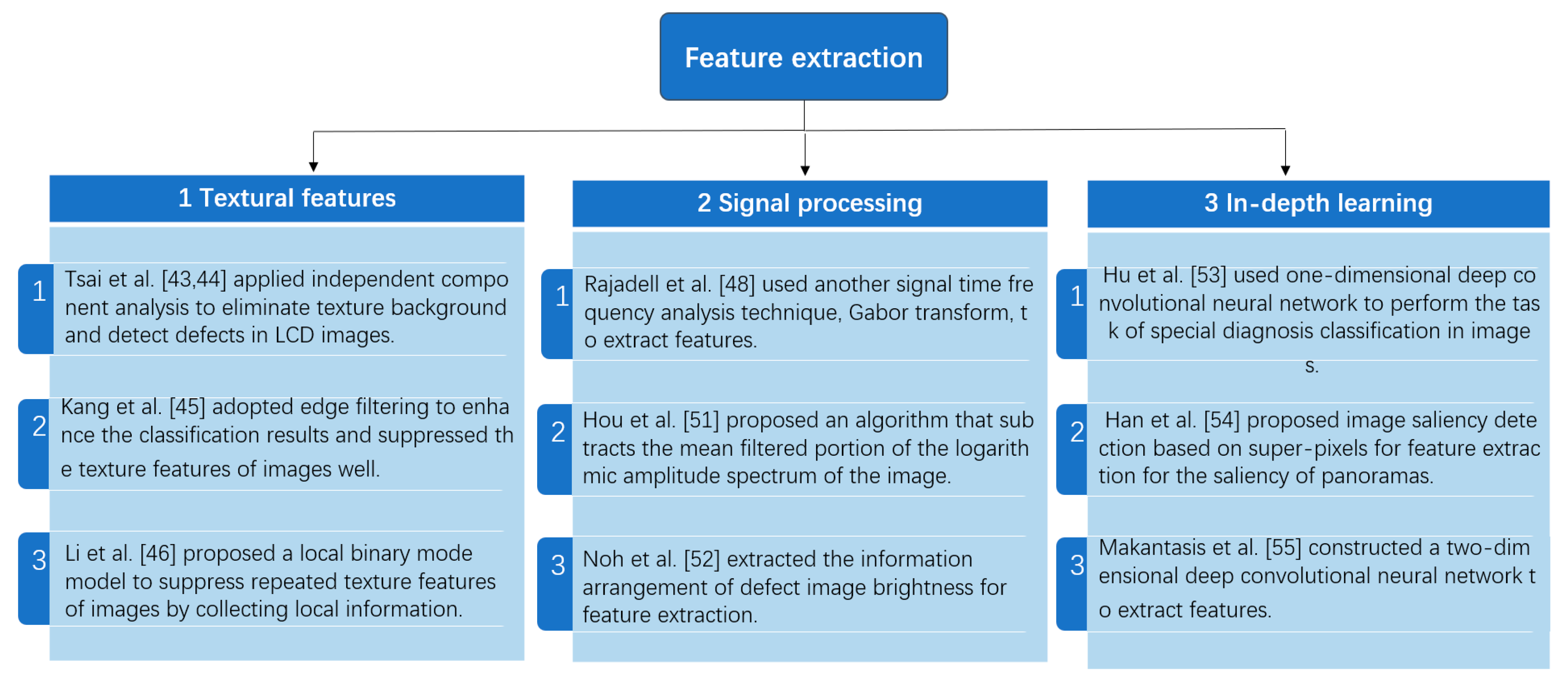
As shown in Figure 8, feature extraction of Mura defects can be performed by using various methods such as texture features, signal processing, and deep learning. Commonly used texture background analysis and suppression methods include texture feature extraction methods based on spatial and frequency domains. Tsai et al. [43,44] applied independent component analysis to eliminate texture background and detect defects in LCD images, and achieved good results. This method was used to detect defects in low contrast textured surface images. Kang et al. [45] adopted edge use edge filtering and multi probability map to enhance the classification results, which had a good suppression of the texture features of the image. The accuracy of image classification was improved from 92% to 96.5%. Li et al. [46] proposed a local binary pattern (LBP) model, which collected local spatial statistical information and semantic information, and completed the suppression of image texture features, thereby completing the extraction of defects, The experimental results show that the classification accuracy of this model is improved by 4%. A wavelet transform based on signal processing is also used to mine the spatial features of image data [47]. Rajadell et al. [48] used a signal time-frequency analysis technique, the Gabor transform, for feature extraction. The accuracy of this method was 92.99%, which was slightly higher than that of Tarabalka [49,50]. Hou et al. [51] proposed an image saliency map extraction algorithm based on spectral residuals and the image’s logarithmic amplitude spectrum minus its mean filtered part was the saliency component of the image. This method is easier to implement in the system and has less computation. Noh et al. [52] treated defect image luminance information of the arrangement, and the results showed that there is a linear relationship between the morphological features and the image area and the degree of interest. The accuracy of image classification by this method reached 90%, but the defect is only partially effective. Deep learning methods have been widely used in Mura defect detection due to their high efficiency in feature extraction and information representation. Hu et al. [53] first introduced the deep learning method in Mura defect detection. They used a one-dimensional depth convolutional neural network to perform special diagnosis classification tasks in images. Han et al. [54] proposed image saliency detection based on super-pixels in feature extraction for the saliency of panoramas. Makantasis [55] et al. used raw data as input to construct a two-dimensional depth convolutional neural network to extract features, which were capable of detecting almost 90% of defects. In addition, semi-supervised deep convolutional neural networks and semi-supervised convolutional recurrent neural networks have also been made to extract the most important information from a limited number of labeled samples.
5.2. Dimension Reduction
The purpose of the dimension reduction algorithm [56] is to extract the most distinguishable image features and the most informative image features by reducing their dimensions. By reducing the dimension of the Mura defect, on the one hand, it can reduce the time complexity and speed up the calculation; on the other hand, it can remove interference and duplicate information, and improve the classification accuracy.
For dimension reduction, the focus of research aims to reduce the dimension of image features data as much as possible without reducing the recognition accuracy, and to increase the speed of image recognition. As shown in Figure 9, the dimension reduction method is mainly divided into linear dimension reduction [57] and non-linear dimension reduction according to the distribution characteristics of the data. The commonly used linear dimension reduction methods mainly include principal component analysis, linear discriminant analysis, and local linear embedding. Non-linear dimension reduction methods mainly include kernel principal component analysis, B-spline fitting, and kernel independent component analysis. The nonlinear dimensionality reduction method maps the nonlinear data to a higher-dimensional space according to the kernel function, and then performs linear dimension reduction on the data in the high-dimensional space.
In the study of linear dimension reduction, the linear discriminant analysis method, proposed by Kang [58], could improve the detection speed and remove image noise. The classification of Mura defects by this method was 86.409%. Tomczak [59] proposed the principal component analysis method, and found that the advantage of the method was that there was no need to use the training set to achieve texture defect detection. But its disadvantage was the fact that it could only reduce the dimension of linear data. For the image dimension reduction of LCD panels containing Mura defects, Liu [60] adopted the local linear embedding method to distinguish Mura image features more significantly. In the study of nonlinear dimension reduction, Liu et al. [60,61] proposed the use of kernel principal component analysis to reduce the dimension to obtain more obvious distinguishing features of panel image pixels. The detection rate of Mura defects by this method was 99.29%. Li [62] proposed B-spline surface fitting with smoothing terms and reduced the dimension of the calculation process, and compressed the amount of vertex data, which greatly improved the accuracy and on-line speed of Mura detection. Fauvel et al. [63] proposed kernel principal component analysis (KPCA) to obtain the principal components, and used a Gaussian kernel to complete the nonlinear subspace mapping, and then completed the dimensionality reduction of the image.
5.3. Summary
This section reviews the features of Mura defect image feature extraction and dimension reduction, as well as related methods. With regard to image feature extraction, three methods can be used: texture feature, signal processing, and deep learning. Among them, the deep learning method is becoming more and more popular because of its excellent effects. By reviewing the dimension reduction methods of Mura defect images, it can be concluded that different kinds of TFT-LCD Mura defects have different characteristics, and the difficulty of recognition is also very different. Thereafter, the corresponding feature extraction methods should be chosen according to the specific defect types.
6. Classifier for Mura Defect
6.1. Principles of Classifiers
The classifier is a means for identifying and classifying the attributes of an image. It can classify objects according to some known characteristics of the image without knowing all the attributes of the image. After the classifier automatically classifies the mathematical model, a large amount of sample data is divided into positive samples and negative samples. The classifier can be divided into various types according to its model.
At present, three main types of classifiers can be used for the Mura defect classification of LCD screens. The first type is LCD defect classifiers based on deep learning [64], and the second type is LCD defect classifiers based on fuzzy pattern recognition [11] the third category is a defect classifier based on support vector machines (SVM) [65]. The advantages and disadvantages of these three classifiers are given in Table 4.
Deep learning [64] has very good learning ability and can achieve large-scale parallel computing by using a variety of computing resources, which has high computing speed and strong computing power. Therefore, it can be used for the classification of LCD Mura defects. The disadvantage of deep learning is that its convergence speed is slow, so the classification takes a long time, which affects the real-time online classification of the LCD screen. In addition, the generalization ability of neural network classification is not glaring, so it is easy to produce over-learning problems, thereby reducing the accuracy of classification.
Fuzzy pattern recognition [11] is often used for the classification of liquid crystal display defects with low contrast, unclear edges of defects, and difficult to distinguish. However, fuzzy pattern recognition has certain limitations, because the effect of fuzzy pattern recognition depends on fuzzy rules. In the fuzzy pattern recognition algorithm, the input variable is the feature of the Mura defect image, and the output variable is the result of classification.
SVM [65] is a kind of algorithm [66,67,68,69], which is creatively produced based on the rigorous structural risk minimization principle proposed in the mid-1990s. It is a better LCD defect classifier at present. Its basic classification principle is to minimize the structural risk of classification. SVM has strong generalization ability, and it can achieve high classification accuracy when using fewer training samples, so it can overcome the curse of dimension and prevent the over-fitting phenomenon. However, the SVM algorithm is sometimes difficult to implement for large-scale training samples.
6.2. Application of Various Classifiers
While adopting an application of fuzzy recognition, Zhang et al. [70] established a fuzzy expert system according to the characteristics of unclear defect edges, and classified the defect grade. Zhang [11] proposed a method based on least square polynomial surface fitting to remove the background to detect Mura defects, and designed a rule-based fuzzy classifier to identify defects. The training of the classifier needs to introduce a lot of feature parameters, which are not suitable for real-time processing. For the classifiers based on deep learning, Zeng et al. [64] adopted the BP neural network to extract and detect Mura defects in experiments, and identified 200 suspected Mura defect images. The results show that the correct detection rate was 98.1%. Among the classifiers based on support vector machines, Liu et al. [71] proposed a high-speed defect recognition system using support vector machine data description for the LCD front substrate manufacturing process, which had a good classification effect. Li et al. [60] proposed 24 kinds of defect features based on shape and texture and classification based on SVM in TFT-LCD defect classification.
Kang et al. [58] conducted an accurate experiment with different classification methods. By comparing four different patterns of Mura defect images, the results of classification by SVM and BP neural network are shown in Figure 10. C1, C2, C3, and C4 are the four types of LCD defects (line and region Mura defects). The average accuracy of the classifier based on the BP network was 86.979%; the average accuracy of the classifier based on SVM was 86.409%. Although the accuracy of the BP neural network is higher, it does not apply to the actual manufacturing process due to its slow learning speed and the risk of converging to a local minimum.
6.3. Summary
There are many types of classifier recognition methods for Mura defects in liquid crystal displays. The classifier based on the neural network has higher recognition accuracy, but it does not apply to the actual manufacturing process due to the limitation of learning ability and the longer recognition time. Fuzzy pattern recognition is not suitable for Mura defect images with high contrast, and it is restricted by fuzzy rules, so it is not suitable for the actual manufacturing process. Because of its strong generalization ability, the classification recognition based on SVM can achieve higher classification accuracy when using fewer training samples, so the comprehensive effect of SVM in Mura defect classification recognition is the best.
7. Discussion
The production process of LCD is divided into three processes. The liquid crystal injection belongs to the cell process, which is a very important part of the production process. In the cell process, there are many reasons for the Mura defect of LCD, most of which are due to the destruction of the molecular arrangement of the injected liquid crystal due to various human factors or external factors [72]. For example: (1) In the process of liquid crystal injection, due to the uneven extrusion pressure on both sides of TFT substrate and color filter substrate, the molecular arrangement of the liquid crystal will be destroyed, resulting in the generation of Mura defect. (2) The injected liquid crystal itself may be mixed with air or other gases for some reason, and corresponding Mura defects will also occur. (3) In the production process, if the bonding is not firm or misplaced, it may cause defects such as liquid crystal leakage. (4) Improper temperature control will also affect the original characteristics of liquid crystals [73].
At the end of the 19th century, Austrian botanists discovered liquid crystals, that is, substances with liquid fluidity and some arrangement characteristics similar to crystals. Under the action of an electric field, the arrangement of liquid crystal molecules will change, which will affect its optical properties. This phenomenon is called the electro-optic effect. Using the electro-optic effect of liquid crystals, British scientists manufactured the first liquid crystal display in the last century [74]. LCD is a kind of display made of liquid crystal. A liquid crystal is a kind of organic compound between solid and liquid. At room temperature, it presents both liquid fluidity and crystal optical anisotropy. It will become transparent liquid when heated and crystalline turbid solid after cooling [75]. Up to now, the discovery of liquid crystal display has developed from poor definition at the beginning to 2K, 4K, and 8K display screens, which also leads to the increasing control accuracy of liquid crystal molecules and more Mura defects.
It could be found the relationship between Mura defect and liquid crystal from the development of liquid crystal display. Sharp (one company in Japan) later transferred the LCD technology patent from radio corporation of America, and successfully developed the calculator, watch, and instrument panel using LCD panel in 1973, which officially opened the era of LCD product application and commercial value [76]. In 1983, Hitachi opened a small black-and-white STN-LCN factory in Kaohsiung [77]. The factory was later expanded into an ASTN LCD factory in 1987, becoming the first black-and-white STN-LCN production line in Taiwan, China. Sharp established a factory in Taichung in 1990 to produce large black-and-white STN LCD [78]. At the same time, the government had made a lot of investment by financing technology development projects. The development of Taiwan’s TFT-LCD industry did not officially begin until 1996 when the government took the industry as the driving force of Taiwan’s economic development. In 2003, SVA and NEC of Japan formally established the first fifth-generation production line on the Chinese mainland. In 2009, through the policies of the government, China merged three major manufacturers (BOE, SVA-NEC, and Taiwan-funded Long-Tung) [79]. In this development process, China has completed the development of LCD from scratch, and also completed the development of LCD from black-and-white screen to color screen and then to OLED screen, which is also the expected effect of liquid crystal molecules from rough use at the beginning to very precise perfusion today. Nowadays, China requires a high refresh rate, high brightness, and high definition of LCD. While completing this requirement, China will have higher requirements for the arrangement of liquid crystal molecules, so the generation of Mura defects is also greatly improved.
8. Outlook
With the rapid development of industrialized machine vision technology, LCDs have become ever more widely used, and Mura defect detection brought by them has also become a huge challenge. This review provides an in-depth description of the main defects in the production of LCDs and summarizes the detection and identification methods of Mura defects. This review identifies the defect classification of LCDs and compares common Mura defects, finally determining the type of Mura defect generated. More importantly, in the process of Mura defect image recognition, from image preprocessing, image dimensionality reduction, feature extraction to final classification and recognition, machine vision is the most important technique The future development trend and research direction of Mura defect detection based on machine vision mainly include the following points:
- (1)
- The traditional manual detection of Mura defects is greatly affected by the state of inspectors and the external environment, with low accuracy and low efficiency. Therefore, the use of machine automation to detect Mura defects is the future development trend, and the combination of machine vision Mura defect detection is one of the key points. In the Mura defect detection of LCDs under machine vision, image processing is particularly important [80,81]. Image collection and processing are greatly affected by external factors. So establishing a stable and reliable detection system is one of the future research directions.
- (2)
- In the filtering and denoising of Mura defects, although the image filtering effect under Gaussian filtering is better. It also has its own coefficient limitations. Therefore, in future image filtering research, overcoming the shortcomings of Gaussian filtering is one of the research directions. In image brightness correction, many methods have their advantages and disadvantages. Hence, combining their various advantages and disadvantages may be one of the future development directions.
- (3)
- Commonly used feature extraction and dimension reduction methods have obvious advantages and disadvantages, and there are also some shortcomings in the image processing of complex Mura defects. Therefore, combining feature extraction and dimension reduction, and rational use of deep learning technology may be one of the future research directions.
- (4)
- The choice of classifier is one of the key points of Mura detection. Commonly used classification methods have certain advantages in one aspect, but their shortcomings are also observable in the other [82]. Therefore, combining the advantages of various classifiers and breaking through their limitations is one of the future research directions.
Author Contributions
Conceptualization, W.M.; methodology, K.L.; software, P.S.; validation, Z.X. and J.Y.; formal analysis, Z.X; investigation, K.L.; resources, X.G.; writing—original draft preparation, S.Z.; writing—review and editing, S.Z.; visualization, X.L.; supervision, W.M.; funding acquisition, X.L. All authors have read and agreed to the published version of the manuscript.
Funding
This research is supported by the Local Innovative and Research Teams Project of Guangdong Pearl River Talents Program (2017BT01G167). Also, it is supported by the Guangdong Provincial Key Laboratory of Manufacturing Equipment Digitization (2020B1212060014) and by the Guangdong Youth Talent Innovation Project (2019GKQNCX092).
Conflicts of Interest
The authors declare no conflict of interest.
References
- Wang, X.; Dong, R.; Li, B. TFT-LCD Mura Defect Detection Based on ICA and Multi-channels Fusion. In Proceedings of the International Conference on Information Science & Control Engineering, Beijing, China, 8–10 July 2016; pp. 687–691. [Google Scholar]
- Yu, W. TFT-LCD liquid crystal display technology and its application. Autom. Instrum. 2001, 22, 25–28. [Google Scholar]
- Mei, S. Research on Mura Defect Image Recognition Algorithm of Lcd Screen Based on Deep Learning. Ph.D. Thesis, Huazhong University of Science and Technology, Wuhan, China, 2017. Available online: https://d.wanfangdata.com.cn/thesis/D01643793. (accessed on 19 October 2021).
- Fan, S.S.; Chuang, Y. Automatic detection of mura defect in tft-lcd based on regression diagnostics. Pattern Recognit. Lett. 2010, 31, 2397–2404. [Google Scholar] [CrossRef]
- Pratt, W.; Sawkar, S.S.; O’Reilly, K.R. Automatic blemish detection in liquid crystal flat panel displays. In Proceedings of the Machine Vision Applications in Industrial Inspection VI, San Jose, CA, USA, 27 January 1998; Volume 3306, pp. 25–30. [Google Scholar]
- Mo, F. Research and Application of TFT-LCD Optical Film. 2013. Available online: https://www.21ic.com/news/opto/201307/228502.htm (accessed on 19 October 2021).
- Yan, C. Research on Mura Defect Detection Technology for TFT-LCD. Master’s Thesis, Hefei University of Technology, Hefei, China, 2017. [Google Scholar] [CrossRef]
- Shi, C. Mobile Phone Screen Defect Detection System Based on Machine Vision. Master’s Thesis, Nanjing University, Nanjing, China, 2014. [Google Scholar] [CrossRef]
- Song, Y.C.; Choi, D.H.; Park, K.H. Multiscale detection of defect in thin film transistor liquid crystal display panel. Jpn. J. Appl. Phys. 2004, 43, 5465–5468. [Google Scholar] [CrossRef]
- Tsai, D.M.; Lin, P.C.; Lu, C.J. An independent component analysis-based filter design for defect detection in low-contrast surface images. Pattern Recogn. 2006, 39, 1679–1694. [Google Scholar] [CrossRef]
- Zhang, Y. Assessment of Operational Feasibility of Waste Vegetable Oil Based Bio-Dielectric Fluid for Sustainable Electric Discharge Machining (Edm) Research on Mura Defect Detection Technology of Tft-Lcd Screen Based on Machine Vision. Ph.D. Thesis, Harbin Institute of Technology, Harbin, China, 2006. [Google Scholar] [CrossRef]
- Jian, C.X.; Gao, J.; Chen, X. A Review of TFT-LCD Panel Defect Detection Methods. Adv. Mater. Res. 2013, 734–737, 2898–2902. [Google Scholar] [CrossRef]
- Qu, H. Research on defect detection of TFT-LCD screen. Optoelectron. Technol. 1997, 17, 102–109. [Google Scholar] [CrossRef]
- Pratt, W.K.; Hawthorne, J.A. Machine vision methods for automatic defect detection in liquid crystal displays. Adv. Imaging 1998, 13, 52–54. [Google Scholar]
- Zhang, P.; Ma, T.T.; Yang, Y.H.; Wang, X.X.; Huang, F.; Tan, S. Mura defect and Measurement Method of Liquid Crystal Display. Electron. Test 2017, 6, 50–52. [Google Scholar]
- SEMI D41-0305. Measurement Method of Semi Mura in Fpd Image Quality Inspection; SEMI: San Jose, CA, USA, 2005. [Google Scholar]
- Chen, C. Computer Image Processing Technology and Algorithm; Tsinghua University Press: Beijing, China, 2003. [Google Scholar]
- Zhang, X.G. Research on the Extraction and Recognition of Defects in the Weld Image of Radiographic Inspection; East China University of Science and Technology: Shanghai, China, 2003; Volume 6, pp. 32–36. [Google Scholar]
- Ji, X. The new development of fluorescent lamp type liquid crystal backlight. Lamps Lighting 2000, 24, 1–4. [Google Scholar]
- Tomasi, C.; Manduchi, R. Bilateral filtering for gray and color images. In Proceedings of the Sixth International Conference on Computer Vision, Bombay, India, 7 January 1998; pp. 839–846. [Google Scholar]
- He, K.; Sun, J.; Tang, X. Guided image filtering. Trans. Pattern Anal. Mach. Intell. 2012, 35, 1397–1409. [Google Scholar] [CrossRef]
- Paris, S.; Durand, F. A fast approximation of the bilateral filter using a signal processing approach. In Proceedings of the European Conference on Computer Vision, Kyoto, Japan, 29 September–2 October 2009; Volume 81, pp. 24–52. [Google Scholar]
- Farbman, Z.; Fattal, R.; Lischinski, D.; Szeliski, R. Edge-preserving decompositions for multi-scale tone and detail manipulation. ACM Trans. Graph. 2008, 27, 67. [Google Scholar] [CrossRef]
- Yuan, S.; Zhao, H.L.; Cao, H.L.; Yi, X.R. Median filtering of noisy images based on MATLAB. Electron. World 2016, 18, 185. [Google Scholar]
- Lin, C.H.; Tsai, J.S.; Chiu, C.T. Switching bilateral filter with a texture/noise detector for universal noise removal. IEEE Trans. Image Process. 2010, 19, 2307–2320. [Google Scholar]
- Golestan, S.; Ramezani, M.; Guerrero, J.M. Moving average filter based phase-locked loops: Performance analysis and design guidelines. IEEE Trans. Power Electron. 2014, 29, 2750–2760. [Google Scholar] [CrossRef] [Green Version]
- Pitas, I.; Venetsanopoulos, A.N. Median filters. Int. Ser. Eng. Comput. Sci. 1992, 84, 63–116. [Google Scholar]
- Geng, G.; Cahill, L.W. An adaptive gaussian filter for noise reduction and edge detection. In Proceedings of the Nuclear Science Symposium and Medical Imaging Conference, San Francisco, CA, USA, 31 October–6 November 1993. [Google Scholar]
- Ding, Y.L. Parallel Processing of Remote Sensing Image Filtering Algorithm Based on CUDA Architecture. Master’s Thesis, PLA Information Engineering University, Zhengzhou, China, 2017. Available online: http://cdmd.cnki.com.cn/article/cdmd-90005-1018702463.htm (accessed on 19 October 2021).
- Cheng, L.M. Research on Mura Defect Detection and Classification Method Based on Machine Vision. Master’s Thesis, Shanghai Jiaotong University, Shanghai, China, 2017. Available online: http://cdmd.cnki.com.cn/article/cdmd-10248-1019654997.htm (accessed on 19 October 2021).
- Chang, D.C.; Wu, W.R. Image contrast enhancement based on a histogram transformation of local standard deviation. IEEE Trans. Med. Imaging 1998, 17, 518–531. [Google Scholar] [CrossRef] [Green Version]
- Taniguchi, K.; Ueta, K.; Tatsumi, S.A. Mura detection method. Pattern Recognit. 2006, 39, 1044–1052. [Google Scholar] [CrossRef]
- Kim, W.; Kwak, D.; Song, Y.; Choi, D.; Park, K. Detection of Spot-Type defects on liquid crystal display modules. Key Eng. Mater. 2004, 270, 808–813. [Google Scholar] [CrossRef]
- Styner, M.; Brechbhler, C.; Szkely, G.; Gerig, G. Parametric estimate of intensity inhomogeneities applied to MRJ. IEEE Trans. Med. Imaging 2000, 19, 153–165. [Google Scholar] [CrossRef] [PubMed]
- Lee, J.Y.; Yoo, S.I. Automatic detection of region-Mura defect in TFT-LCD. IEICE Trans. Inf. Syst. 2004, 87, 2371–2378. [Google Scholar]
- Choi, K.; Park, N.; Yoo, S.J. Image restoration for quantifying TFT-LCD defect levels. IEICE Trans. Inf. Syst. 2008, 91, 322–329. [Google Scholar] [CrossRef] [Green Version]
- Oppenheim, A.; Schafer, R. Homomorphic analysis of speech. IEEE Trans. Audio Electroacoust. 1968, 16, 221–226. [Google Scholar] [CrossRef]
- Ryu, J.S.; Oh, J.H.; Kim, J.G.; Koo, T.M.; Park, K.H. TFT-LCD panel Blob-Mum inspection using the correlation of wavelet coecients. In Proceedings of the IEEE Region 10 Conference, Chiang Mai, Thailand, 24 November 2004. [Google Scholar]
- Song, Y.C.; Choi, D.H.; Park, K.H. Wavelet-based image enhancement for defect detection in thin film transistor liquid crystal display panel. Jpn. J. Appl. Phys. 2006, 45, 5069–5072. [Google Scholar] [CrossRef]
- Chen, L.C.; Kuo, C.C. Automatic TFT-LCD Mura defect inspection using discrete cosine transform-based background filtering and just noticeable difference quantification strategies. Meas. Sci. Technol. 2007, 19, 015507. [Google Scholar] [CrossRef] [Green Version]
- Chen, S.L.; Chou, S.T. TFT-LCD Mura defect detection using wavelet and cosine transforms. J. Adv. Mech. Des. Syst. Manuf. 2008, 2, 441–453. [Google Scholar] [CrossRef]
- Park, N.K.; Latecki, L.J.; Mount, D.M.; Choi, K.N.; Yoo, S.I.; Wu, A.Y. Quantification of line Mura defect levels based on multiple characterizing features. Electron. Imaging 2006, 6066, 3–8. [Google Scholar]
- Tsai, D.M.; Tseng, Y.H.; Chao, S.M.; Yen, C.H. Independent component analysis based filter design for defect detection in low-contrast textured images. In Proceedings of the 18th International Conference on Pattern Recognition, Hong Kong, China, 20–24 August 2006; Volume 2, pp. 231–234. [Google Scholar]
- Lu, C.; Tsai, D. Independent component analysis-based defect detection in patterned liquid crystal display surfaces. Image Vis. Comput. 2008, 26, 955–970. [Google Scholar] [CrossRef]
- Kang, X.; Li, S.; Benediktsson, J.A. Spectral-Spatial hyperspectral image classification with edge-preserving filtering. IEEE Trans. Geosci. Remote Sens. 2014, 52, 2666–2677. [Google Scholar] [CrossRef]
- Li, W.; Chen, C.; Su, H.; Du, Q. Local binary patterns and extreme learning machine for hyperspectral imagery classification. Int. J. Precis. Eng. Manuf.-Green Technol. 2015, 53, 3681–3693. [Google Scholar] [CrossRef]
- Bruce, L.M.; Koger, C.H.; Jiang, L. Dimensionality reduction of hyperspectral data using discrete wavelet transform feature extraction. IEEE Trans. Geosci. Remote Sens. 2002, 40, 2331–2338. [Google Scholar] [CrossRef]
- Rajadell, O.; Garcia-Sevilla, P.; Pla, F. Spectral-Spatial pixel characterization using gabor filters for hyperspectral image classification. IEEE Geosci. Remote Sens. Lett. 2013, 10, 860–864. [Google Scholar] [CrossRef] [Green Version]
- Tarabalka, Y.; Chanussot, J.; Benediktsson, J. Segmentation and classification of hyperspectral images using watershed transformation. Pattern Recognit. 2010, 43, 2367–2379. [Google Scholar] [CrossRef] [Green Version]
- Tarabalka, Y.; Chanussot, J.; Benediktsson, J. Segmentation and classification of hyperspectral images using minimum spanning forest grown from automatically selected markers. IEEE Trans. Syst. Man Cybern. 2010, 40, 1267–1279. [Google Scholar] [CrossRef] [PubMed] [Green Version]
- Hou, X.; Zhang, L. Saliency detection: A spectral residual approach. In Proceedings of the 2007 IEEE Conference on Computer Vision and Pattern Recognition, Minneapolis, MN, USA, 17–22 June 2007; Volume 1, pp. 1–8. [Google Scholar]
- Noh, C.; Lee, S.; Kim, D.; Chung, C. Effective defect classification for flat display panel film images. In Proceedings of the International Conference on Convergence and Hybrid Information Technology, Daejeon, Korea, 27–29 August 2009; pp. 264–267. [Google Scholar]
- Hu, W.; Huang, Y.; Wei, L.; Zhang, F.; Li, H. Deep learning for remote sensing image understanding. J. Sens. 2016, 2, 1–12. [Google Scholar]
- Han, B.J.; Sim, J.Y. Saliency detection for panoramic landscape images of outdoor scenes. J. Vis. Commun. Image Represent. 2017, 49, 27–37. [Google Scholar] [CrossRef]
- Makantasis, K.; Karantzalos, K.; Doulamis, A.; Doulamis, N. Deep supervised learning for hyperspectral data classification through convolutional neural networks. In Proceedings of the IEEE International Geoscience and Remote Sensing Symposium, Milan, Italy, 26–31 July 2015; pp. 4959–4962. [Google Scholar]
- Zhuang, J. Research on Spatial Spectrum Feature Extraction and Dimension Reduction of Hyperspectral Images Based on Variable Gabor. Master’s Thesis, Shenzhen University, Shenzhen, China, 2020. [Google Scholar]
- Somol, P.; Pudil, P.; Novoviˇcová, J.; Paclık, P. Adaptive floating search methods in feature selection. Pattern Recognit. Lett. 1999, 20, 1157–1163. [Google Scholar] [CrossRef]
- Kang, S.B.; Lee, J.H.; Song, K.Y.; Pahk, H.J. Automatic defect classification of TFT-LCD panels using machine learning. In Proceedings of the 2009 IEEE International Symposium on Industrial Electronics, Seoul, Korea, 5–8 July 2009; IEEE: Piscataway Township, NJ, USA, 2009. [Google Scholar]
- Tomczak, L.; Mosorov, V.; Sankowski, D.; Nowakowski, J. Image defect detection methods for visual inspection systems. In Proceedings of the 2007 9th International Conference—The Experience of Designing and Applications of CAD Systems in Microelectronics, Lviv, Ukraine, 19–24 February 2007. [Google Scholar]
- Liu, Y.; Huang, Y.; Lee, M. Automatic inline defect detection for a thin film transistor-liquid crystal display array process using locally linear embedding and support vector data description. Meas. Sci. Technol. 2008, 19, 095501. [Google Scholar] [CrossRef]
- Liu, Y.; Wang, C.; Ting, Y.; Lin, W.; Kang, Z.; Chen, C. In-TFT-array-process micro defect inspection using nonlinear principal component analysis. Int. J. Mol. Sci. 2009, 10, 4498–4514. [Google Scholar] [CrossRef] [Green Version]
- LI, K. Mura Defect Detection Method Based on B-Spline Surface Fitting and Snake Model. Master’s Thesis, University of Electronic Science, Chengdu, China, 2014. [Google Scholar]
- Fauvel, M.; Chanussot, J.; Benediktsson, J.A. Kernel principal component analysis for the classification of hyperspectral remote sensing data over urban areas. EURASIP J. Adv. Signal Process. Vol. 2009, 783, 194. [Google Scholar] [CrossRef] [Green Version]
- Zeng, Y.; Guo, L.; Luo, B. Mura defect detection method for TFT-LCD based on BP neural network and mean difference. J. Hunan Inst. Sci. Technol. 2017, 30, 32–38. [Google Scholar]
- Wang, H. Research on Defect Imaging, Extraction, Recognition and Classification of Tft-Lcd Panel. Master’s Thesis, Hefei University of Technology, Hefei, China, 2019. [Google Scholar]
- Vapnik, V.N. The Nature of Statistical Learning Theory; Springer: Berlin/Heidelberg, Germany, 1995; p. 203. [Google Scholar]
- Cortes, C.; Vapnik, V. Support vector networks. Mach. Learn. 1995, 20, 273–297. [Google Scholar] [CrossRef]
- Cortes, C. Prediction of Generalization Ability in Learning Machines; Department of Computer Science, University of Rochester: Rochester, NY, USA, 1995. [Google Scholar]
- Chen, B.; Fan, X.; Zhou, Z.; Li, X. Principle and prospect of support vector machine. Manuf. Autom. 2010, 32, 136–138. [Google Scholar]
- Zhang, Y.; Zhang, J. Fuzzy recognition of the defect of TFT-LCD. Int. Soc. Opt. Eng. 2005, 5637, 233–240. [Google Scholar]
- Liu, Y.; Liu, Y.; Chen, Y. High-speed inline defect detection for TFT-LCD array process using a novel support vector data description. Expert Syst. Appl. 2011, 38, 6222–6231. [Google Scholar] [CrossRef]
- Khullar, S.; Zhou, C.; Feng, J.J. Dynamics of Topological Defects around Drops and Bubbles Rising in a Nematic Liquid Crystal. Phys. Rev. Lett. 2007, 99, 237802. [Google Scholar] [CrossRef] [Green Version]
- Bellini, T.; Chiccoli, C.; Pasini, P.; Zannoni, C. Monte carlo study of liquid-crystal ordering in the independent-pore model of aerogels. Phys. Rev. E 1996, 54, 2647. [Google Scholar] [CrossRef] [Green Version]
- Liu, D. Study on Positioning of Super Twisted Liquid Crystal Grating. Master’s Thesis, Guizhou University, Guizhou, China, 2009. [Google Scholar] [CrossRef]
- Lu, Y.X. Iterative evolution of liquid crystal display (LCD) industry. Fine Spec. Chem. 2018, 26, 5–12. [Google Scholar] [CrossRef]
- Wang, S.C. Value Innovation; China Productivity Center: Taipei, Taiwan, 2003. [Google Scholar]
- Hsiao, C.T.; Chang, P.L.; Ho, S.P. Applying evolutionary perspective to analyse the TFT-LCD industry development in Taiwan. Syst. Res. Behav. Sci. 2011, 28, 283–300. [Google Scholar] [CrossRef]
- Chen, Y.J.; Chen, J.H. Using Systems Dynamics View to Investigate TFT-LCD Industrial Development Process in Taiwan. In Proceedings of the 2006 ITRI Conference on Innovation and Technology Management, Taiwan, China, 21–23 June 2006. [Google Scholar]
- Hsiao, C.T. A systems view for the high-tech industry development: A case study of large-area TFT-LCD industry in Taiwan. Asian J. Technol. Innov. 2011, 19, 117–132. [Google Scholar] [CrossRef]
- Ming, W.; Shen, F.; Zhang, Z.; Du, J.; Chen, Z.; Cao, Y. A comprehensive review of defect detection in 3c glass components. Measurement 2020, 158, 107722. [Google Scholar] [CrossRef]
- Ming, W.; Shen, F.; Zhang, H.; Li, X.; Lu, Y. Defect detection of LGP based on combined classifier with dynamic weights. Measurement 2019, 143, 211–225. [Google Scholar] [CrossRef]
- Ming, W.; Cao, C.; Zhang, G.; Zhang, H.; Zhang, F.; Jiang, Z.; Yuan, J. Application of Convolutional Neural Network in Defect Detection of 3C Products. IEEE Access 2021, 9, 135657–135674. [Google Scholar] [CrossRef]
Figure 1.
Development process of liquid crystal display technology, from the earliest principle to the current universal application.
Figure 1.
Development process of liquid crystal display technology, from the earliest principle to the current universal application.

Figure 2.
Statistical chart of global TFT-LCD demand in recent years.

Figure 3.
Manufacturing process of TFT-LCD.

Figure 4.
Diagram of TFT structure.

Figure 5.
Schematic diagram of common Mura defects [3]. Reprinted with permission from ref. [3], Copyright 2017 Huazhong University of Science and Technology.

Figure 6.
Flow chart of automatic optical inspection of TFT-LCD Mura defect [3]. Reprinted with permission from ref. [3], Copyright 2017 Huazhong University of Science and Technology.

Figure 7.
Image brightness nonuniformity processing [30]. Reprinted with permission from ref. [30]. Copyright 2013 Precision Engineering.

Figure 8.
Common feature extraction for Mura defects methods.

Figure 9.
Comparative of linear dimension reduction and nonlinear dimension reduction.

Figure 10.
Accuracy comparison between SVM and BP neural network.


Table 1.
Common causes of Mura defects in the manufacturing process.
| Process Stage | Causes of Mura Defects |
|---|---|
| Array process | Substrate scratches, breakage, chipping, bubbles, etc. [7] |
| Uneven color of filter [8] | |
| Cell process | Impurity in liquid crystal [8] |
| The material characteristics of filter substrate are not uniform [1] | |
| Scan line short circuit, open circuit [8] | |
| Polarizer anisotropy | |
| Uneven liquid crystal distribution [1] | |
| Different local characteristics of TFT array substrate | |
| Module process | Uneven brightness of backlight module |
| Module assembly extrusion [7] | |
| Uneven brightness of light source [1] | |
| Uneven distribution of light source | |
| Uneven optical film [8] |
Table 2.
Comparison of Mura defect detection methods.
| Defect Detection Method | Advantages | Disadvantages |
|---|---|---|
| Manual detection method | It has better flexibility in the detection of Mura defects [3]. | The detection efficiency is low, and the manual detection speed cannot keep up with the production speed of the production line; there is a great subjectivity, and external factors will also have a great influence under high production costs. |
| Electrical measurement method | It has high efficiency in Mura defect detection. | Unable to determine the precise location and type of the defect, it takes a long time [13]. |
| Optical measurement method based on machine vision | It can detect Mura defects caused by non-electrical reasons such as chemical pollution. It is a non-contact detection method [5,15]; high accuracy. | The equipment cost is high and requires trained professionals to operate [16]. |
Table 3.
Methods based on the spatial and frequency domains.
| Method | Applications | Advantages | Disadvantages | |
|---|---|---|---|---|
| Spatial-based method | The gray-scale histogram-based correction method [31] | Taniguchi et al. [32] utilized gray-scale linear mapping to enhance the image brightness in the spatial domain; Kim [33] et al. applied the method of estimating the optimal mean and standard deviation to correct and enhance the image brightness. | Histogram equalization can adjust the gray dynamic range of the image to achieve the purpose of brightness correction and enhancement. | Prone to over-enhancement, loss of details |
| The background fitting method [34] | Lee et al. [35] adopted an improved regression diagnosis method to fit the LCD background with Mura defects to eliminate the influence of uneven background; Choi et al. [36] employed the principal component analysis (PCA) method, based on the statistical characteristics of the image, the defect features were retained, and the background degradation such as uneven background and virtual focus in the LCD image was eliminated. | Subtract the fitted background image from the original image to achieve better brightness correction | This method is computationally intensive. | |
| Frequency-based method | Homomorphic filtering method [37] | Ryu et al. [38] adopted the discrete wavelet transform method to decompose the LCD image. By comparing the decomposition coefficients, the significant and insignificant coefficients were separated, the uneven background was eliminated, and the fuzzy spots Mura were identified; Song et al. [39] proposed a wavelet-based image preprocessing method; Chen et al. [40,41] adopted background filtering based on discrete cosine transform to detect Mura defects. | The homomorphism filtering method converts the multiplicative brightness field of the image into an additive brightness field, and eliminates the inhomogeneity of the brightness field through filtering, which has been well applied in the image brightness correction. | It will produce a blur effect on the image boundary, and the frequency domain filter type and parameters must be selected appropriately. |
Table 4.
Comparison of classifiers for Mura defects.
| Types of Classifiers | Advantages | Disadvantages |
|---|---|---|
| Neural deep learning | Learning ability is very good, through the use of a variety of computing resources, to achieve large-scale parallel computing, which has a high computing speed and strong computing power. | The convergence speed is slow, so the classification takes a long time, which affects the real-time online classification of LCD. It is easy to have overlearning and affect the accuracy of classification. |
| Fuzzy pattern | It can be used for defect classification with low specific intensity, unclear edges, and is difficult to distinguish. | The effect of fuzzy pattern recognition depends on fuzzy rules. |
| Support Vector Machines | The structural risk is small, the generalization ability is strong, and a higher classification accuracy can be achieved when using fewer training samples for training. | Difficult to implement for large-scale training samples |
Publisher’s Note: MDPI stays neutral with regard to jurisdictional claims in published maps and institutional affiliations. |
© 2021 by the authors. Licensee MDPI, Basel, Switzerland. This article is an open access article distributed under the terms and conditions of the Creative Commons Attribution (CC BY) license (https://creativecommons.org/licenses/by/4.0/).
Share and Cite
MDPI and ACS Style
Ming, W.; Zhang, S.; Liu, X.; Liu, K.; Yuan, J.; Xie, Z.; Sun, P.; Guo, X. Survey of Mura Defect Detection in Liquid Crystal Displays Based on Machine Vision. Crystals 2021, 11, 1444. https://0-doi-org.brum.beds.ac.uk/10.3390/cryst11121444
AMA Style
Ming W, Zhang S, Liu X, Liu K, Yuan J, Xie Z, Sun P, Guo X. Survey of Mura Defect Detection in Liquid Crystal Displays Based on Machine Vision. Crystals. 2021; 11(12):1444. https://0-doi-org.brum.beds.ac.uk/10.3390/cryst11121444
Chicago/Turabian StyleMing, Wuyi, Shengfei Zhang, Xuewen Liu, Kun Liu, Jie Yuan, Zhuobin Xie, Peiyan Sun, and Xudong Guo. 2021. "Survey of Mura Defect Detection in Liquid Crystal Displays Based on Machine Vision" Crystals 11, no. 12: 1444. https://0-doi-org.brum.beds.ac.uk/10.3390/cryst11121444
Note that from the first issue of 2016, this journal uses article numbers instead of page numbers. See further details here.