
Recent Advances in Fabricating Wurtzite AlN Film on (0001)-Plane Sapphire Substrate


Institute of Semiconductors, Guangdong Academy of Sciences, Guangzhou 510650, China
*
Authors to whom correspondence should be addressed.
Crystals 2022, 12(1), 38; https://doi.org/10.3390/cryst12010038
Submission received: 30 November 2021
/
Revised: 21 December 2021
/
Accepted: 22 December 2021
/
Published: 27 December 2021
(This article belongs to the Special Issue Wide Bandgap Semiconductor Materials and Devices)
Abstract
:Ultrawide bandgap (UWBG) semiconductor materials, with bandgaps far wider than the 3.4 eV of GaN, have attracted great attention recently. As a typical representative, wurtzite aluminum nitride (AlN) material has many advantages including high electron mobility, high breakdown voltage, high piezoelectric coefficient, high thermal conductivity, high hardness, high corrosion resistance, high chemical and thermal stability, high bulk acoustic wave velocity, prominent second-order optical nonlinearity, as well as excellent UV transparency. Therefore, it has wide application prospects in next-generation power electronic devices, energy-harvesting devices, acoustic devices, optical frequency comb, light-emitting diodes, photodetectors, and laser diodes. Due to the lack of low-cost, large-size, and high-ultraviolet-transparency native AlN substrate, however, heteroepitaxial AlN film grown on sapphire substrate is usually adopted to fabricate various devices. To realize high-performance AlN-based devices, we must first know how to obtain high-crystalline-quality and controllable AlN/sapphire templates. This review systematically summarizes the recent advances in fabricating wurtzite AlN film on (0001)-plane sapphire substrate. First, we discuss the control principles of AlN polarity, which greatly affects the surface morphology and crystalline quality of AlN, as well as the electronic and optoelectronic properties of AlN-based devices. Then, we introduce how to control threading dislocations and strain. The physical thoughts of some inspirational growth techniques are discussed in detail, and the threading dislocation density (TDD) values of AlN/sapphire grown by various growth techniques are compiled. We also introduce how to achieve high thermal conductivities in AlN films, which are comparable with those in bulk AlN. Finally, we summarize the future challenge of AlN films acting as templates and semiconductors. Due to the fast development of growth techniques and equipment, as well as the superior material properties, AlN will have wider industrial applications in the future.
1. Introduction
As a representative ultrawide bandgap (UWBG) semiconductor material, wurtzite aluminum nitride (AlN) material has many excellent properties such as high electron mobility (1100 cm2/Vs), high breakdown voltage (11.7 MV/cm), high piezoelectric coefficient, high thermal conductivity (320 W/m·K), high hardness (nine on the Mohs scale), high corrosion resistance, high chemical and thermal stability, as well as high bulk acoustic wave velocity (11,270 m/s) [1,2,3]. Therefore, it is quite suitable to fabricate next-generation power electronic devices, energy harvesting devices, and acoustic devices that can operate in the harsh environment [4,5,6]. The device frequency can be further increased to a quite high level by alloying with scandium nitride (ScN), because AlScN material has a larger electromechanical coupling and piezoelectric coefficient [7]. Due to the prominent second-order optical nonlinearity, AlN is also an attractive nonlinear optical material for optical frequency comb (OFC) application that enables on-chip wavelength conversion [8]. The wideband transparency of AlN allows it to work in ultraviolet and visible regions, unlike the Si platform that only works at long wavelengths [9]. Besides, AlN has a small thermal and lattice mismatch with the high-Al-composition AlGaN materials, as well as excellent transparency in the ultraviolet region. Thus, it is suitable to fabricate AlGaN-based deep-ultraviolet (DUV) light-emitting diodes (LEDs), photo-detectors (PDs) and laser diodes (LDs) [10,11,12]. In the dual role of the Minamata Convention on Mercury and COVID-19 [13,14], the market capacity of AlGaN-based DUV LEDs has reached 160 million USD in 2020, although the wall-plug efficiency (WPE) of industrial-grade DUV LEDs is still below 10% [10]. Undoubtedly, AlN material will have broad application prospects in the future.
AlN crystal has three possible structures: hexagonal wurtzite structure, cubic zinc blende structure, and rock salt structure [15]. Among them, metastable-phase cubic zinc blende structure and rock salt structure only exist in some special growth conditions. In most cases, the hexagonal wurtzite structure is needed because its excellent chemical stability is helpful to obtain highly reliable devices. However, the high chemical stability makes it quite challenging to grow high-crystalline-quality bulk AlN crystals. Growing bulk crystals from the melt, which is performed for most other III–V semiconductors, is no longer applicable to AlN because ultrahigh temperature and pressure are needed. Nowadays, bulk AlN crystals are nearly exclusively obtained by using the physical vapor transport (PVT) method (sublimation and recondensation), which has achieved low TDDs of 102–105 cm−2 [2]. Nevertheless, it still cannot solve the typical problems such as small size (<60 mm), high impurity concentration (1018–1019 cm−3), poor ultraviolet transparency (α265–280 nm = 14–21 cm−1), and high cost (>9000 USD/2 inch) [16]. Only a few companies can supply bulk AlN in the world, and the production capacity is very low due to the very long growth time and very low yield. As an alternative, depositing thin AlN films on foreign substrates such as sapphire, silicon (Si), and silicon carbide (SiC) has become the prevailing method to obtain AlN crystals [17,18,19]. These pseudo-substrates are also called AlN templates. Among them, the most commonly used foreign substrate is sapphire, which is commercially available in various sizes (2–8 inches) and surface orientations (c, m, r, and a planes). Importantly, the crystalline quality of AlN/sapphire template is relatively good, and the cost of AlN/sapphire template has been reduced to 250 USD/2 inch. The deposition methods include metal organic chemical vapor deposition (MOCVD), molecular beam epitaxy (MBE), hydride vapor phase deposition (HVPE), physical vapor deposition (PVD), pulsed laser deposition (PLD), and atomic layer deposition (ALD).
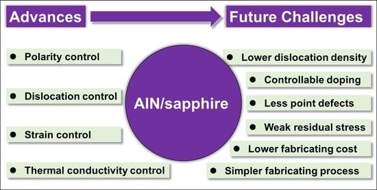
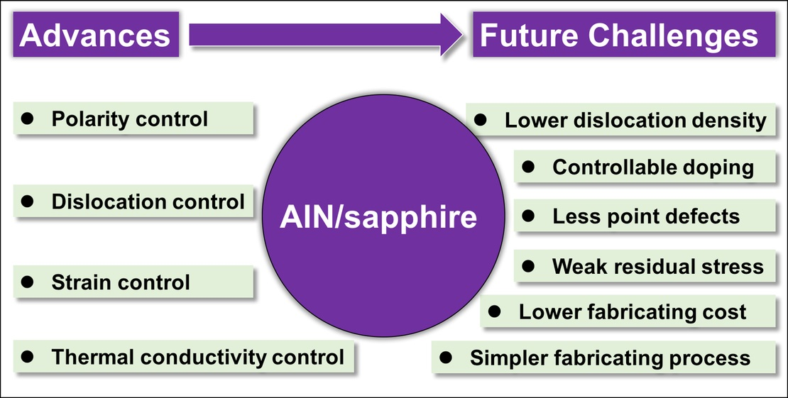
In this article, we focus on reviewing the research advances in fabricating wurtzite AlN films on sapphire substrates. We will introduce the control principles of polarity, dislocations, strain, and thermal conductivity. Finally, we will summarize the future challenge of AlN films from the aspect of template and semiconductor.
2. Polarity Control of AlN/Sapphire Template
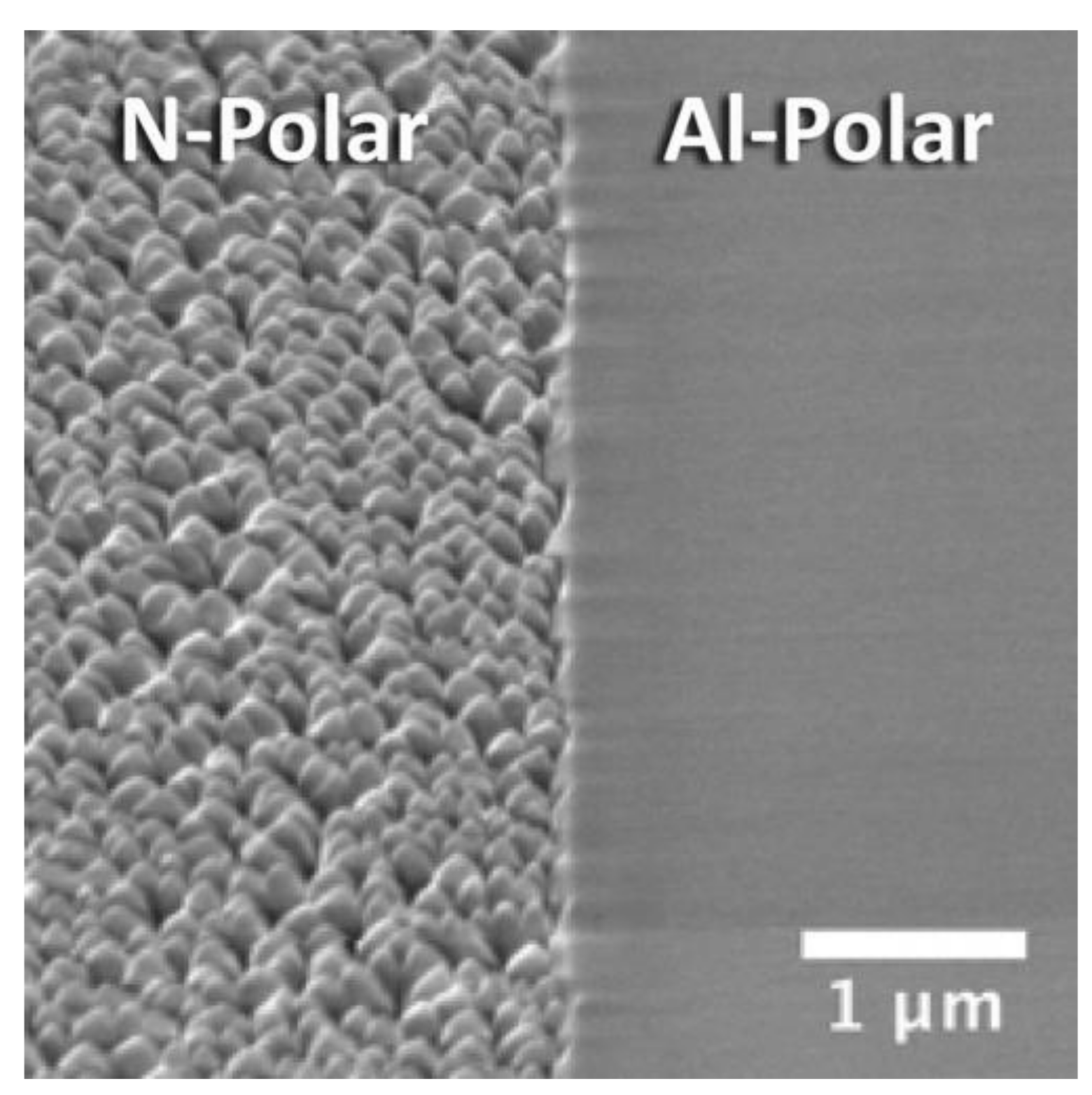
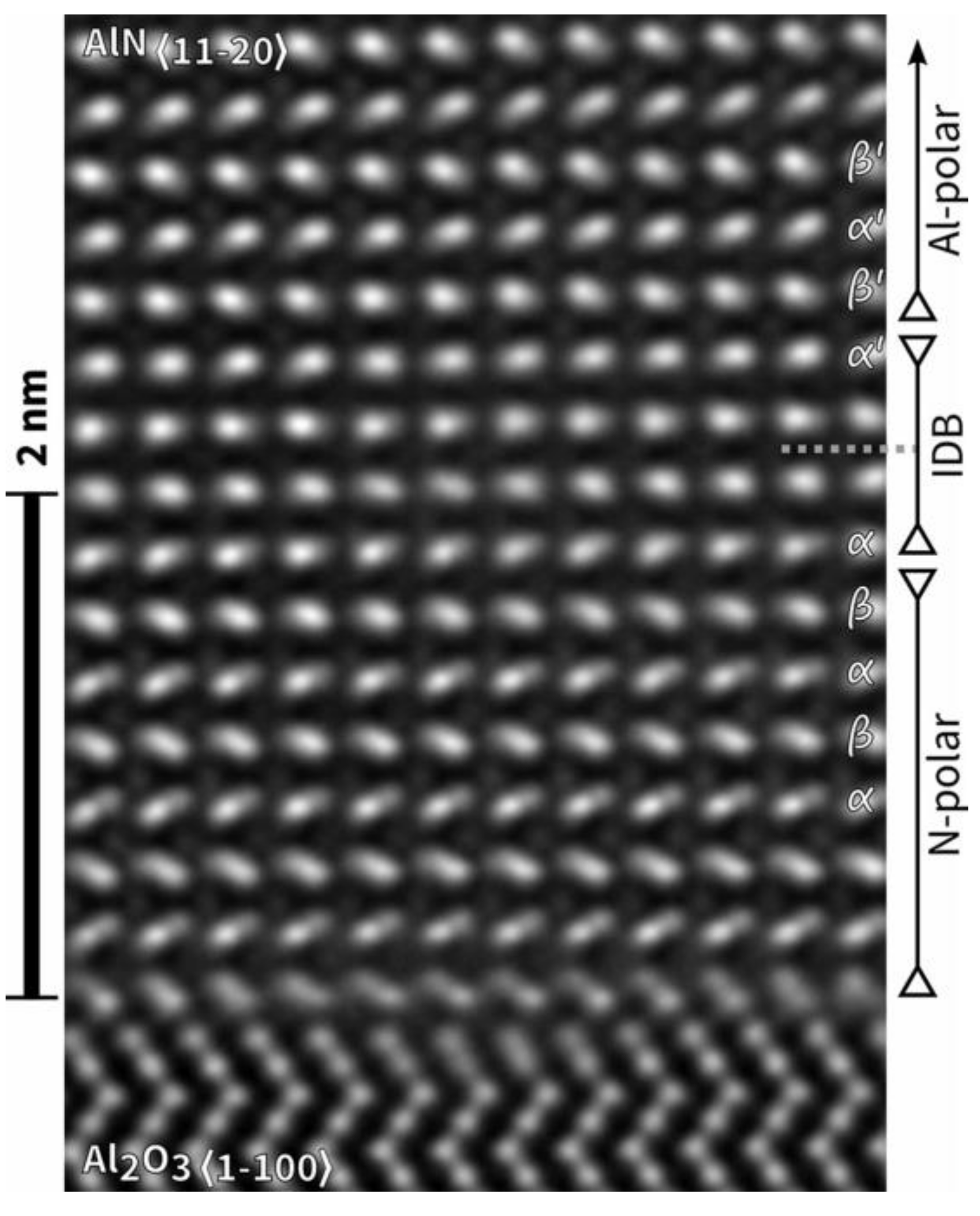
The polarity control is very important for AlN-based devices, because polarity greatly affects the electronic and optoelectronic properties by changing the pyroelectric and piezoelectric fields [20]. The polarities of AlN include Al-polarity (+c-polarity) and N-polarity (−c-polarity). Except for some special applications such as lateral polarity structure (LPS) and N-polar high electron mobility transistors (HEMTs) [21,22], N-polar AlN is not desired because of its poor crystalline quality, surface morphology, and chemical stability. Ronny Kirste et al. demonstrated the surface of N-polar AlN was dominated by a typical columnar morphology, with an average width of ~500 nm and a height difference of ~100 nm [23], as shown in Figure 1. The rough surface morphology originated from the presence of Al-polar inversion domains (IDs), which had a faster growth rate along the [0001] direction. Other studies have also confirmed that N-polar AlN usually coexists with Al-polar AlN IDs, meaning that AlN film grown on sapphire substrate generally exists in two forms: Al-polar AlN and mixed-polar AlN. To realize large-area pure N-polar AlN, C-face SiC substrate may be the better choice [24]. The mixed-polar AlN can be confirmed by the KOH solution etching because N-polar AlN has an obvious faster etching rate compared with Al-polar AlN. Figure 2 displays some etched surfaces of AlN epilayers grown in different conditions [25]. The etched parts are N-polar AlN, and the residual parts are Al-polar AlN.
Compared with other nitride semiconductors, the polarity control of AlN film grown on sapphire substrate is much more difficult. It is attributed to the formation of unevenly distributed aluminum-oxynitride (AlxOyNz) phases near the AlN/sapphire interface, which is responsible for the appearance of mixed-polar AlN. AlxOyNz phases can exist with various stoichiometric ratios, depending on the competition result of Al, O, and N atoms [26]. Since the 1970s, various AlxOyNz phases have been established, including 20H (Al10O3N8), 27R (Al9O3N7), 16H (Al8O3N6), 21R (Al7O3N5), 12H (Al6O3N4), and many other phases [27]. These O atoms may come from sapphire substrate, precursors and chambers, so they are hard to completely eliminate. To suppress the undesired N-polar AlN/mixed-polar AlN, we need to find out the key factors affecting polarity control in the presence of O atoms.
H. D. Sun et al. found that proper TMAl pretreatment promoted the formation of Al-polar AlN, because carbon (C) impurities dissociated from TMAl precursor could attract surrounding O impurities and suppress the formation of AlxOyNz phases [28]. Cross-sectional energy-loss spectroscopy spectrum (EELS) demonstrated that the distributions of C and O atoms above the AlN/sapphire interface are highly consistent. J. M. Wang et al. found that 7 s NH3 preflow (nitridation) could also maintain Al-polar AlN, and the c-axis orientation was very good [29]. However, a longer-time NH3 preflow resulted in the formation of mixed-polar AlN. Obviously, the pretreatment process before the deposition of AlN film is very important. Additionally, it was found that high initial growth temperature facilitates the formation of N-polar AlN. Reina Miyagawa et al. revealed that a certain chemical reaction occurred during the high-temperature growth process, causing the exchange of O atoms in sapphire substrate and N atoms in AlN epilayer in some areas [30]. As a result, Al-polar and N-polar AlN simultaneously appeared and coexisted in the subsequent growth process, because the large N-polar AlN grains at high growth temperature were hard to bury.
In some special cases, the transition from pure N-polar or mixed-polar AlN to pure Al-polar AlN may occur. Stefan Mohn et al. demonstrated that pure N-polar AlN could be entirely converted into Al-polar AlN within 3 nm, with the help of a flat rhombohedral AlxOyNz layer [31]. Scanning transmission electron microscope (STEM) and high-resolution transmission electron microscopy (HRTEM) images revealed that the conversion had been completed during the nitridation process before growth, as shown in Figure 3. However, excessive annealing may destroy the AlxOyNz structure, leading to incomplete coverage of the AlxOyNz layer, especially when the annealing temperature is very high. In this situation, the undesirable mixed-polar AlN is formed due to the incomplete conversion of N-polar AlN to Al-polar AlN. Mitsuru Funato et al. reported that N-polar AlN domains in mixed-polar AlN could be buried by their surrounding Al-polar AlN, as shown in Figure 4. This phenomenon occurred when the nitridation of sapphire substrate initiated at a low temperature of 100 °C [32]. The elimination of N-polar AlN domains benefited from the small size of inversion domains and the faster growth rate of Al-polar AlN [25]. Based on the above analysis, we can see that the realization of pure Al-polar AlN has three approaches: suppressing the local formation of AlxOyNz phases in the initial stage, converting N-polar to Al-polar AlN by the complete coverage of ultrathin AlxOyNz layer, and burying N-polar AlN by the lateral overgrowth of Al-polar AlN.
3. Dislocation and Strain Control of AlN/Sapphire Template
The TDD value is one of the most important indexes for AlN/sapphire template, because it has an obvious impact on the device performance. For example, the internal quantum efficiency (IQE) of the defect-sensitive DUV LEDs is inversely proportional to the TDD value. If we want to obtain an IQE value approaching 100%, the TDD value usually needs to be reduced to 1 × 107 cm−2 [33]. Besides, the TDD value directly affects the reverse leakage and breakdown voltage of photodetectors and electronic device. It has been demonstrated that AlGaN-based avalanche photodiode (APD) achieves an extremely high breakdown field of 9 MV/cm and a quite low dark current of 0.1 pA@-340 V, when a bulk AlN substrate with an extremely low TDD of 103 cm−2 is adopted [34]. Strain management is also important for AlN/sapphire template. The strain in AlN/sapphire template is usually induced by lattice and thermal mismatch, and the mismatch stress in AlN film can even reach the order of GPa. During the growth process, the strain may cause wafer bowing, surface roughening, cracking, and peeling off. Wafer bowing will further affect the thickness and composition uniformity of the upper AlGaN materials, and surface roughening will hinder the formation of steep interface. Additionally, the residual strain in epilayer also brings difficulty in device fabrication and reliability control. Therefore, it is very important to control dislocation and strain in AlN/sapphire template. Over the past 30 years, many growth techniques have been developed to solve this problem.
In the beginning, due to the lack of high-temperature (HT) growth equipment, pulsed atomic layer epitaxy (PALE) growth technique, and its derivatives such as migration-enhanced epitaxy (MEE), modified MEE, and migration-enhanced metal organic chemical vapor deposition (MEMOCVD) were widely adopted to enhance the migration ability of Al adatoms [35,36,37]. The pulsed growth technique can be simply divided into two types: (i) NH3 pulsed growth technique; (ii) double-precursor pulsed growth technique. The NH3 pulsed growth technique can reach extremely low V/III ratio and the best surface diffusion of Al adatoms by always keeping the TMAl precursor on. This technique made it possible to grow AlN at relatively low growth temperature (<1100 °C) using the conventional MOCVD and MBE equipment, but the surface of the as-grown AlN often exhibited macro-steps [38,39]. The double-precursor pulsed growth technique means that pulsed TMAl and NH3 are completely or partially separately supplied to adjust the surface diffusion of Al adatoms and suppress the gas phase reaction between the precursors. Usually, the so-called MEE, modified MEE, and MEMOCVD belong to the double-precursor pulsed growth technique. R. G. Banal et al. reported that a 600 nm-thick AlN grown by modified MEE technique achieved low FWHM values of 45 and 250 arcsec for (0002) and (10−12) plane, respectively [36]. Max Shatalov et al. used 10 μm-thick AlN/sapphire template grown by MEMOCVD technique to realize an DUV LED with an external quantum efficiency of 10.4% at 20 mA CW current, which reached a record high value at that time [40]. However, the process window of the pulsed growth technique is very narrow, and the experimental results strongly depend on the growth equipment. Therefore, they are very hard to repeat by other groups. In addition, the pulsed growth technique suffers from relatively low growth rates, further limiting its industrial application. Recently, with the rapid development of HT growth equipment, many new growth techniques have been proposed to obtain high-crystalline-quality and weak-residual-strain AlN film. Importantly, they demonstrate better growth repeatability, and thus have important reference value.
3.1. Two-Step Growth (TSG)
Two-step growth (TSG) technique was first proposed in 1986 to grow high-quality GaN epilayer on sapphire substrate. The main processes of TSG technique include low-temperature (LT) nucleation and high-temperature (HT) growth. Besides, there also exists an important in situ annealing process between them. The LT nucleation process aims to form high-density small three-dimensional (3D) islands by promoting vertical growth over lateral growth. During the in situ annealing process, the decomposition of GaN will happen at energetically unstable or highly faulted regions, and then GaN will be redeposited on other places to form large isolated 3D islands [41]. After that, the HT growth process can utilize lateral growth from these inclined side facets to promote dislocation bending and annihilation, significantly improving the crystalline quality of GaN epilayer grown on sapphire substrate. The quasi-two-dimensional (quasi-2D) growth after the coalescence of 3D islands facilitates the achievement of smooth surface. Combined with the subsequent breakthrough in p-type GaN, GaN-based blue LEDs developed rapidly to the commercial application level, triggering the revolution of general illumination. In 2014, the Nobel Prize for Physics was awarded to Akasaki, Amano, and Nakamura for such great progress. Today, many other growth techniques for III-nitrides are actually the evolution of this technique.
As for AlN material, however, the TSG technique is not so effective. First, the chemical stability of AlN is better, so the decomposition of AlN need to be performed in higher annealing temperature. Second, the chamber pressure is usually very low during AlN growth to restrain gas phase pre-reactions, so the decomposition of AlN is further suppressed during the in situ annealing process. Third, due to a higher diffusion barrier, the Al adatoms after decomposition can hardly migrate to areas with potential energy minima. Therefore, large isolated 3D islands cannot be formed by decomposition and redeposition of AlN, as shown in Figure 5 [41]. In the subsequent HT growth process, the lateral growth of AlN is inadequate, so dislocations can hardly bend and interact with each other. Generally, the threading dislocation density (TDD) values are in the level of 109–1010 cm−2. Despite this, the TSG technique is still used because of its simple and low-cost process.
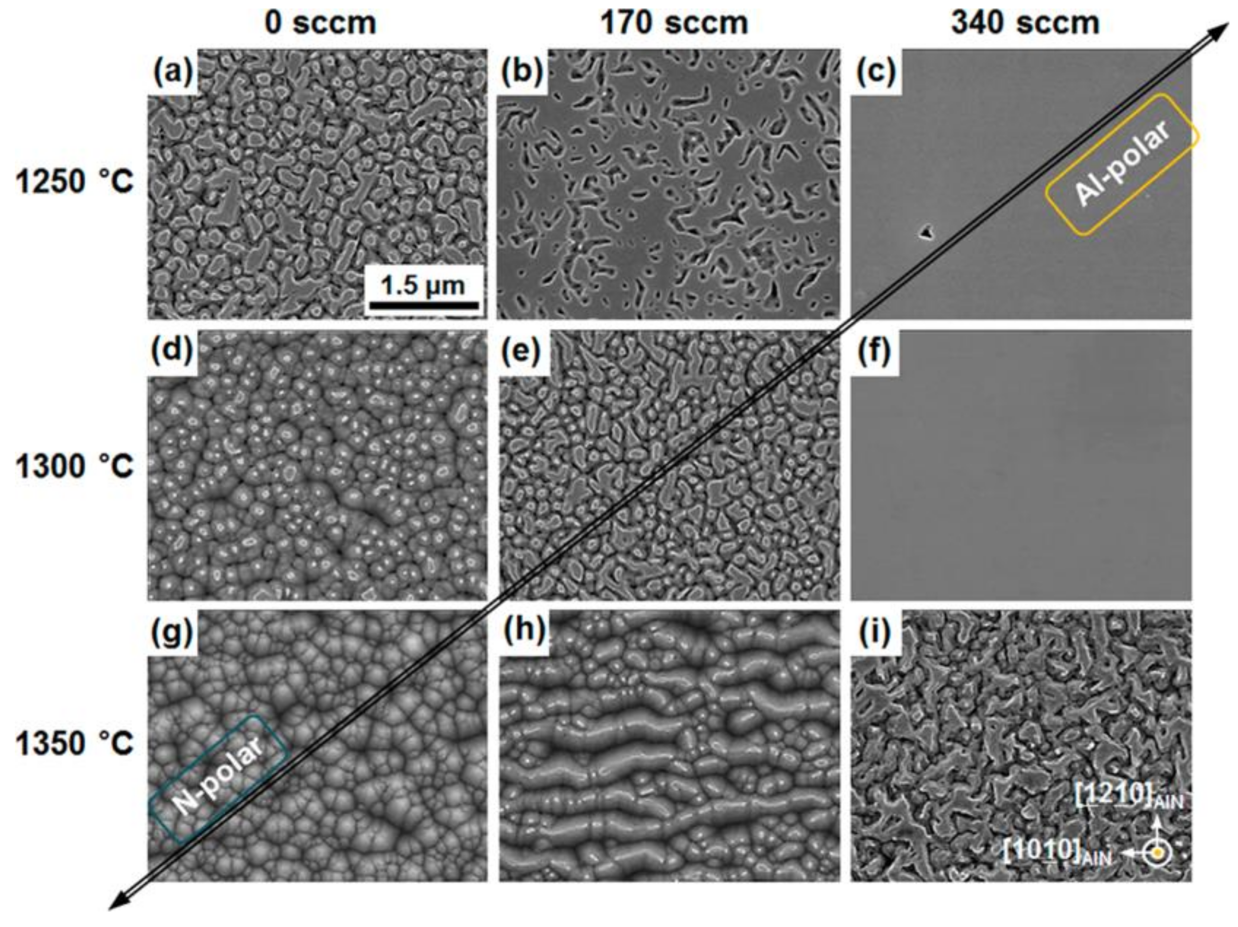
Recently, our group has found that adopting large-offcut-angle sapphire substrate can significantly improve the crystalline quality of the AlN epilayer grown by the TSG technique [42]. The physical reason is macro-steps tend to appear on the large-offcut-angle sapphire substrate, and dislocations are easy to lock and drag by the edges of macro-steps, resulting in the inclination and interaction with other dislocations. Therefore, we can control and regulate dislocation behaviors by adjusting the densities and geometric features of macro-steps, as shown in Figure 6. It is found that high-density zigzag macro-steps are significantly effective for decreasing TDD, because they can induce dislocation inclination towards multiple directions. The inclination angles can be increased to 30–78°, so the lateral interaction range of dislocations demonstrate a sixfold increase. As a result, the full-width at half maximum (FWHM) values of X-ray (0002) and (10−12) -plane rocking curves (RCs) for the 1 μm-thick AlN were reduced down to 115 and 364 arcsec, corresponding to a TDD value of 1.4 × 109 cm−2. It demonstrates an 80% decrease compared with its counterpart grown on 0.2°-off sapphire substrate. However, the stress control is still a problem for thick film due to the lack of stress-releasing channels.
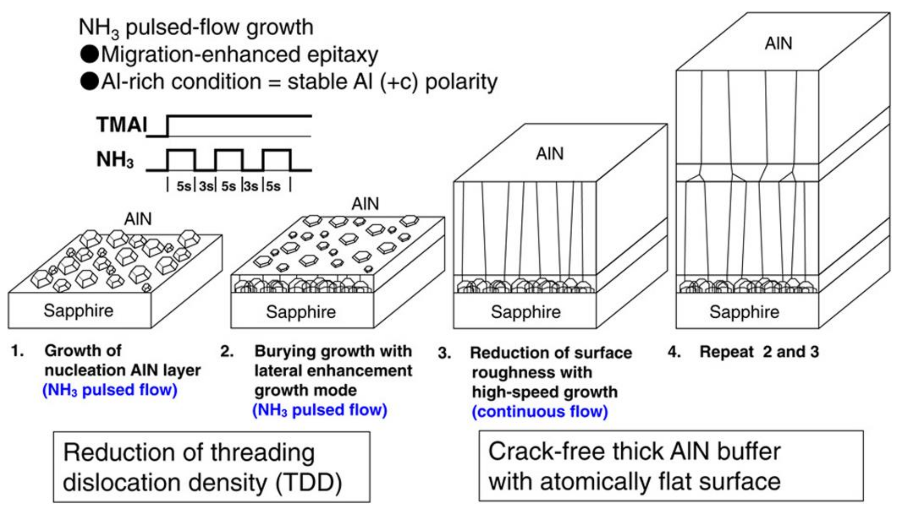
3.2. Multiple-Step Growth (MSG)
To strengthen dislocation interactions during 3D–2D transition process, which are insufficient for TSG technique, a multiple-step growth (MSG) technique was proposed to modify the growth modes of AlN epilayer. Hirayama et al. demonstrated that a 4.8 μm-thick high-quality AlN epilayer could be obtained by adopting a five-step NH3 pulse-continuous flow alternating technique, as shown in Figure 7 [43]. The FWHM values of X-ray (0002) and (10−12) -plane RCs were 200 and 370 arcsec, respectively. Meanwhile, the AlN surface is crack-free and smooth. The core idea is repeatedly alternating pulsed flow and continuous low to repeat 3D–2D growth and introduce multiple “rough-to-smooth” processes. Actually, a rough surface can also be realized by low growth temperature, high V/III mole ratio, and large TMAl flow. Conversely, a smooth surface can be obtained.
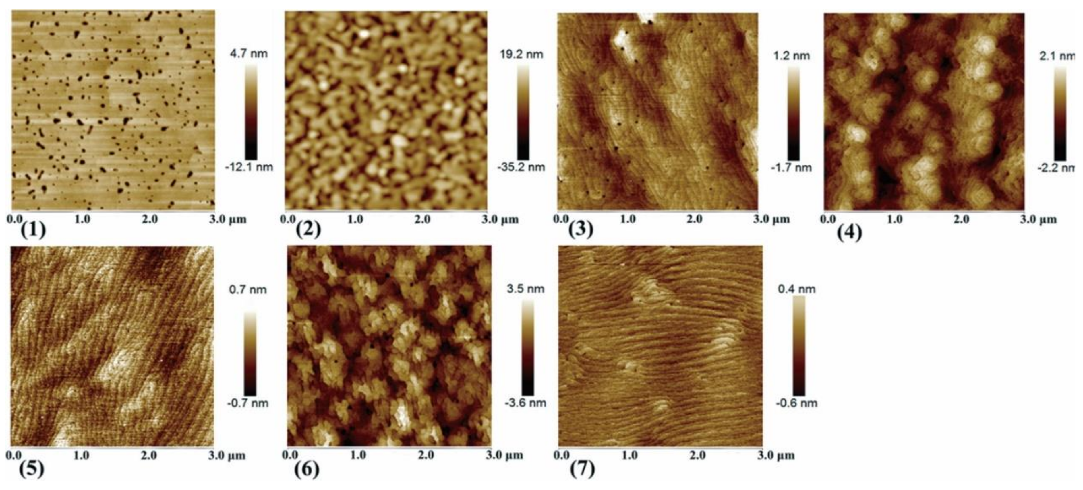
The MSG technique is easy to be repeated by other groups. On the above basis, many other groups also developed their own techniques and apply them to fabricate high-performance devices. For example, X. Zhang et al. developed a low-temperature and high-temperature (LT-HT) alternating technique to obtain high-quality crack-free AlN epilayer [44]. AFM images in Figure 8 display that the surface morphology of AlN epilayer experiences three “rough-to-smooth” processes and finally becomes atomically smooth. The FWHM values of X-ray (0002) and (10−12) -plane RCs for the 2.9 μm-thick AlN epilayer were 311 and 548 arcsec, respectively. Importantly, they also found that the first 3D–2D cycle play a major role in reducing TDD and the subsequent 3D–2D cycles mainly account for the relaxation of tensile stress. Y. R. Chen et al. demonstrated that a three-cycle MSG technique could be used to fabricate high-performance solar-blind ultraviolet (SUV) PDs due to the improved crystalline quality, surface morphology, and residual stress. The back-illuminated SUV PD exhibited a low dark current density of 5.56 × 10⁻⁷ A/mm2 at −10 V and a high responsivity of 0.15 A/W at 271 nm [45]. J. C. Yan et al. adopted a three-cycle MSG technique to realize a 50% reduction in TDD in AlN epilayer. As a result, the light output power (LOP) of the 285 nm DUV LED based on MSG technique exceeds 3 mW at 20 mA driving current [46].
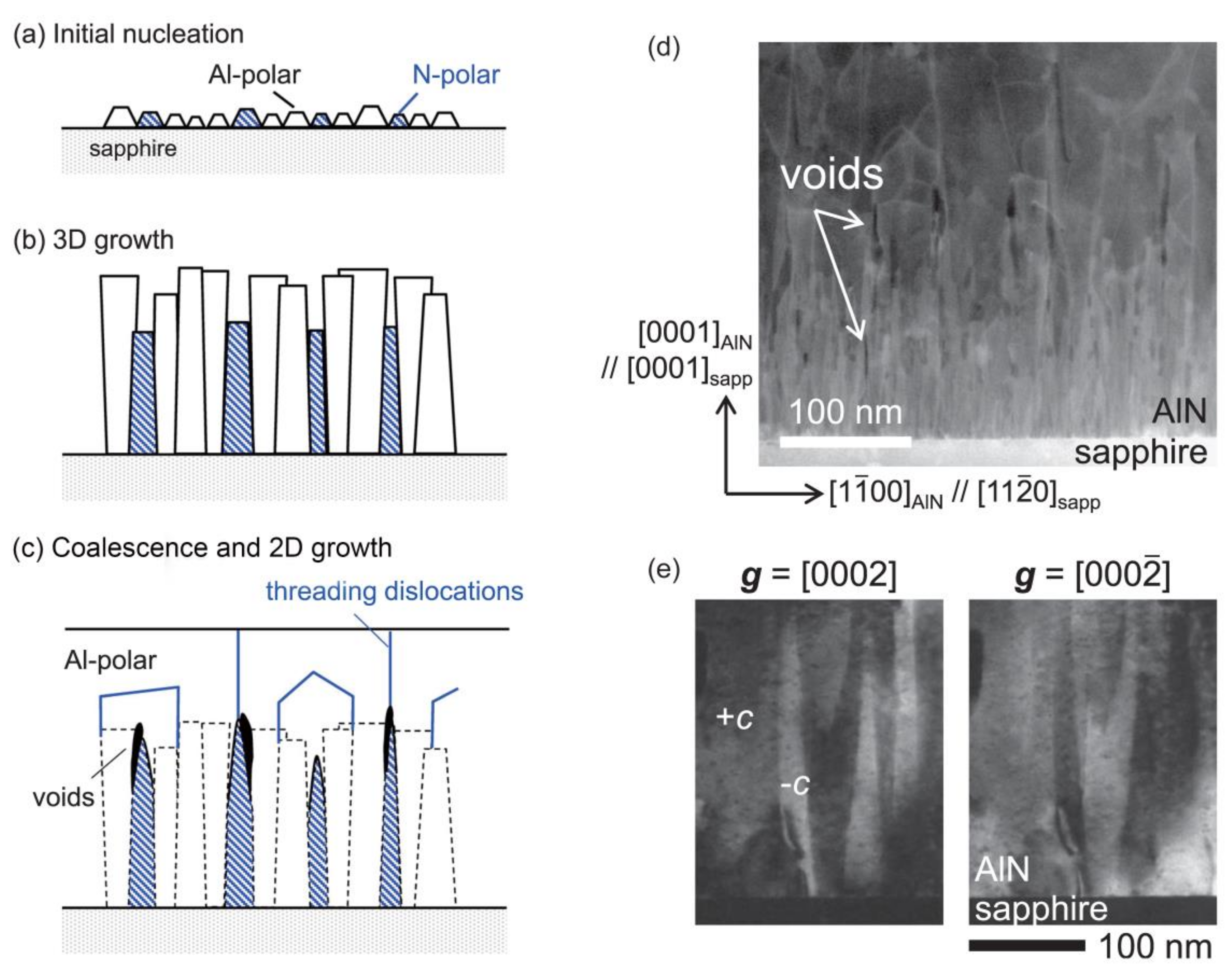
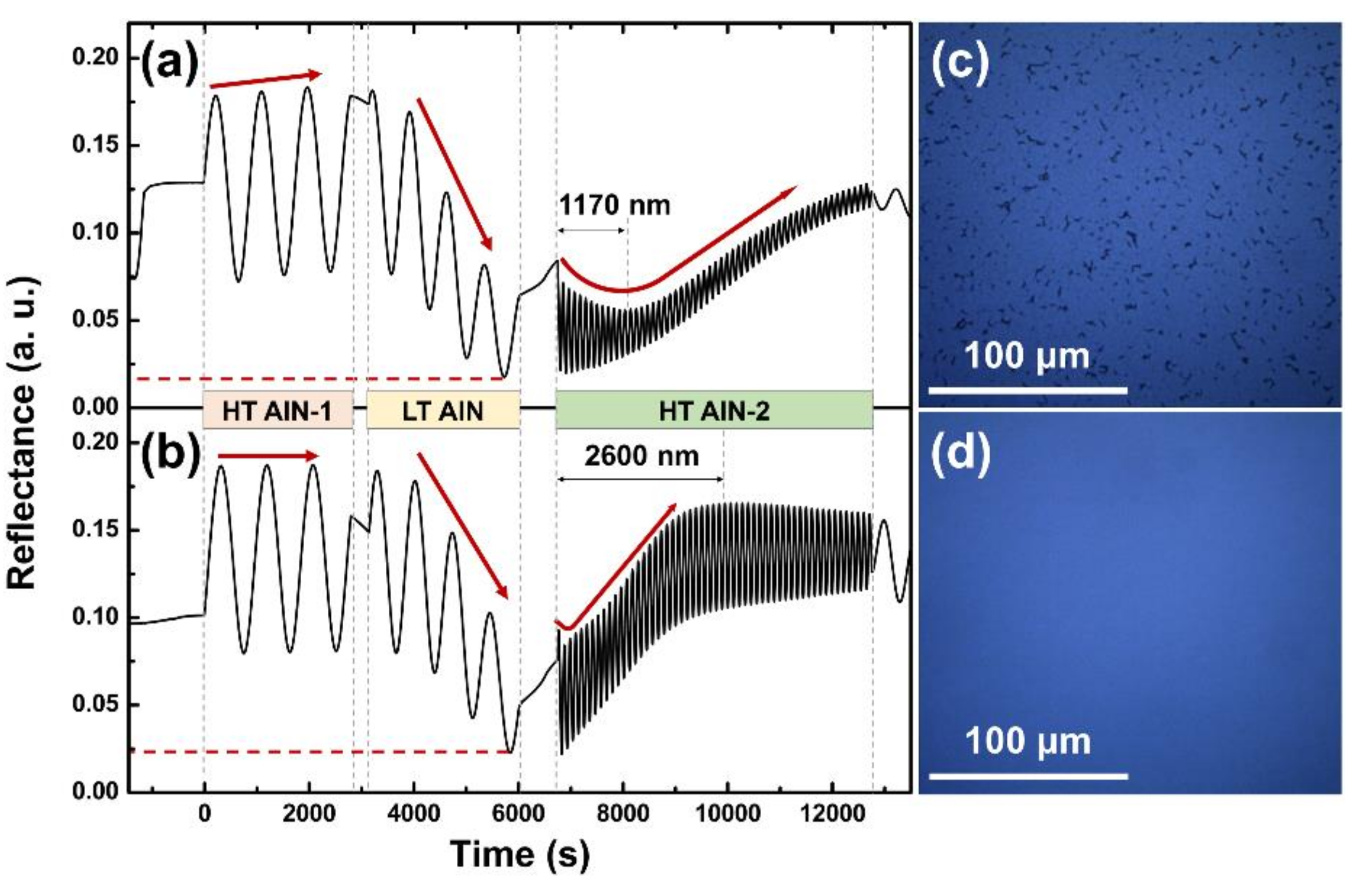
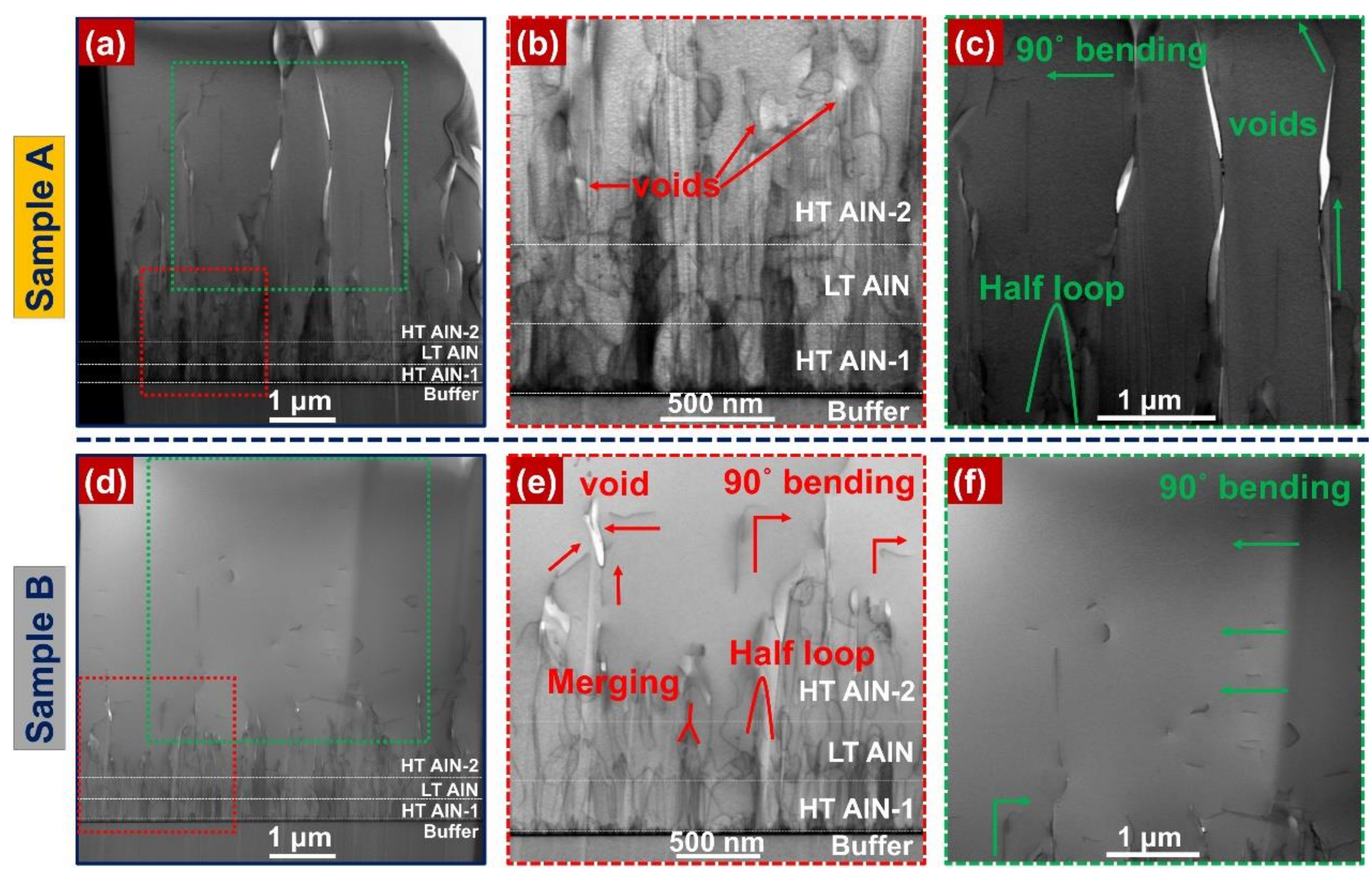
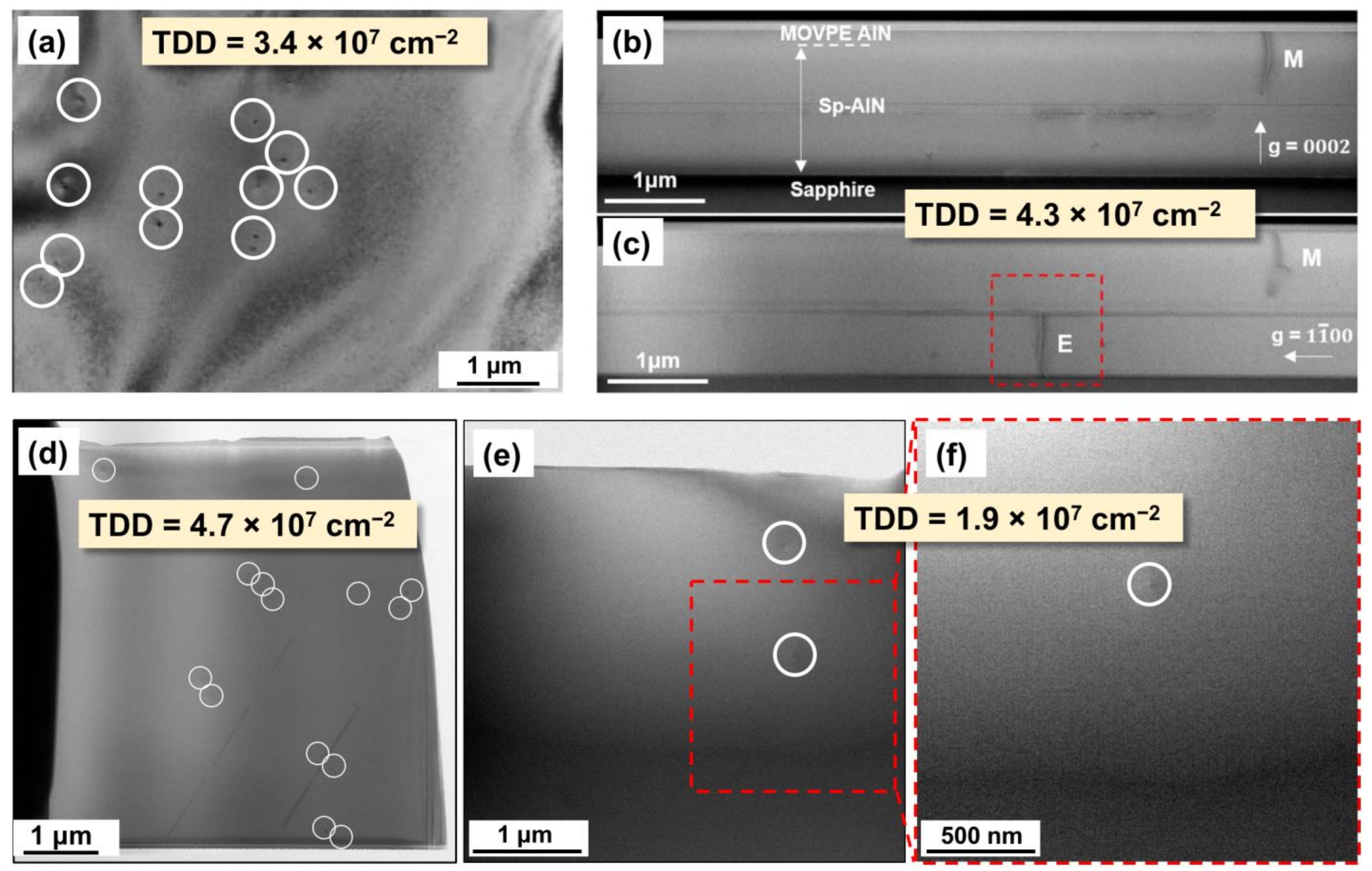
Our group found that high-quality AlN could be obtained by only using one LT interlayer. The physical thought was first using LT interlayer to maximize the 3D growth process, and then using high temperature and large TMAl flow to realize surface flattening. To achieve this goal, we chose sputtered AlN buffer rather than the conventional MOCVD AlN buffer, as shown in Figure 9 [47,48]. The high lateral coverage speed and large depth/width ratio between adjacent 3D islands even induce the formation of nano-voids, and the density and geometric features of nano-voids can be tuned by modifying the growth modes [17,49,50,51]. When the density of nano-voids reaches 1.7 × 1010 cm−2, they could provide sufficient free surfaces for dislocation termination, which was clearly observed in the cross-sectional STEM images (Figure 10) [17]. Moreover, the excellent c-axis orientation of nano-voids means new dislocations near the coalescence boundaries were effectively suppressed. Thus, a 5.6 μm-thick four-step AlN layer with a TDD value of 4.7 × 107 cm−2 was obtained. Meanwhile, the high-density nano-voids significantly released the tensile stress from 0.50 to 0.18 GPa during the growth process [52]. It is attributed that the high-density nano-voids can effectively destroy the interaction between sapphire substrate and AlN epilayer by reducing the contact area. This advantage allowed us to obtain 11.0 μm-thick crack-free AlN epilayer, wherein the TDD value was further decreased to 1.9 × 107 cm−2.
3.3. Epitaxial Lateral Overgrowth (ELOG)
As mentioned above, the physical thought behind the MSG technique is to produce proper 3D side facets during growth for dislocation bending and interaction. We can also produce numerous broader side faces by patterning sapphire substrate or template, in which situation dislocations are more easily bent by the image face from the persistent side faces. The growth technique on patterned sapphire substrate (PSS) or patterned template is usually called epitaxial lateral overgrowth (ELOG), which is essential to realize entire surface coalescence. This method has been widely used in the MOCVD growth of GaN, including using SiO2/SiNx patterned mask and commercially available PSS. Unlike GaN, however, SiO2/SiNx patterned mask is not suitable for AlN growth. The large adhesive coefficient of Al adatom on SiO2/SiNx surface makes AlN demonstrate random growth rather than selective growth. Therefore, only patterned sapphire substrate, patterned AlN/sapphire template, or patterned AlGaN template can be adopted.
In 2006, M. Imura et al. demonstrated the ELOG of AlN on patterned AlN/sapphire templates with 2 μm-deep and 3 μm-wide trenches [53,54]. To realize entire surface coalescence within a thinner layer, the extension direction of the trenches should be along [11-20]sapphire direction rather than [10-10]sapphire direction [55]. Plan-view TEM showed that the TDD of ELOG-AlN could be reduced down to an extremely low value of 3.4 × 107 cm−2. However, the TDD in the coalescence boundaries above the trenches was much higher than that in other regions, so the dislocation distribution was inhomogeneous. It is a common feature of ELOG on trench-patterned substrate/template, which has also been found in other material systems. Moreover, due to the poor migration ability of Al adatoms, the 3 μm-wide spacing between the adjacent patterns requires a large thickness of 10 μm to realize flat surface morphology and low TDD. H. Long et al. reported that pyramidal PSS (diameter = 1 μm, period = 2 μm) could induce a dual coalescence of AlN. Accordingly, air-voids were generated twice, promoting dislocation termination and stress relaxation twice [56]. Although the coalescence process of microscale ELOG can be tuned by controlling growth temperature, V/III ratio and substrate miscut, the typical coalescence thickness of AlN on patterned sapphire/template is still >5 μm. In some cases, the coalescence thickness even reaches 10 μm [56,57,58]. Thus, long growth time and high cost are needed.
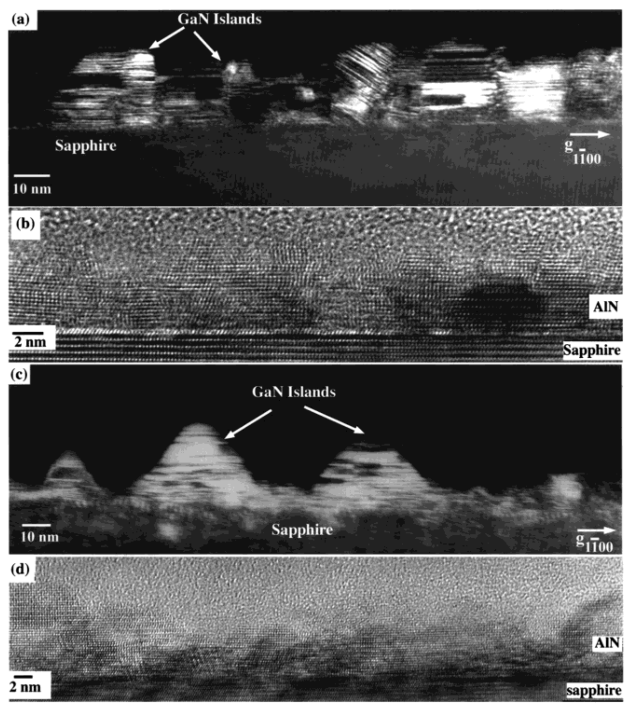
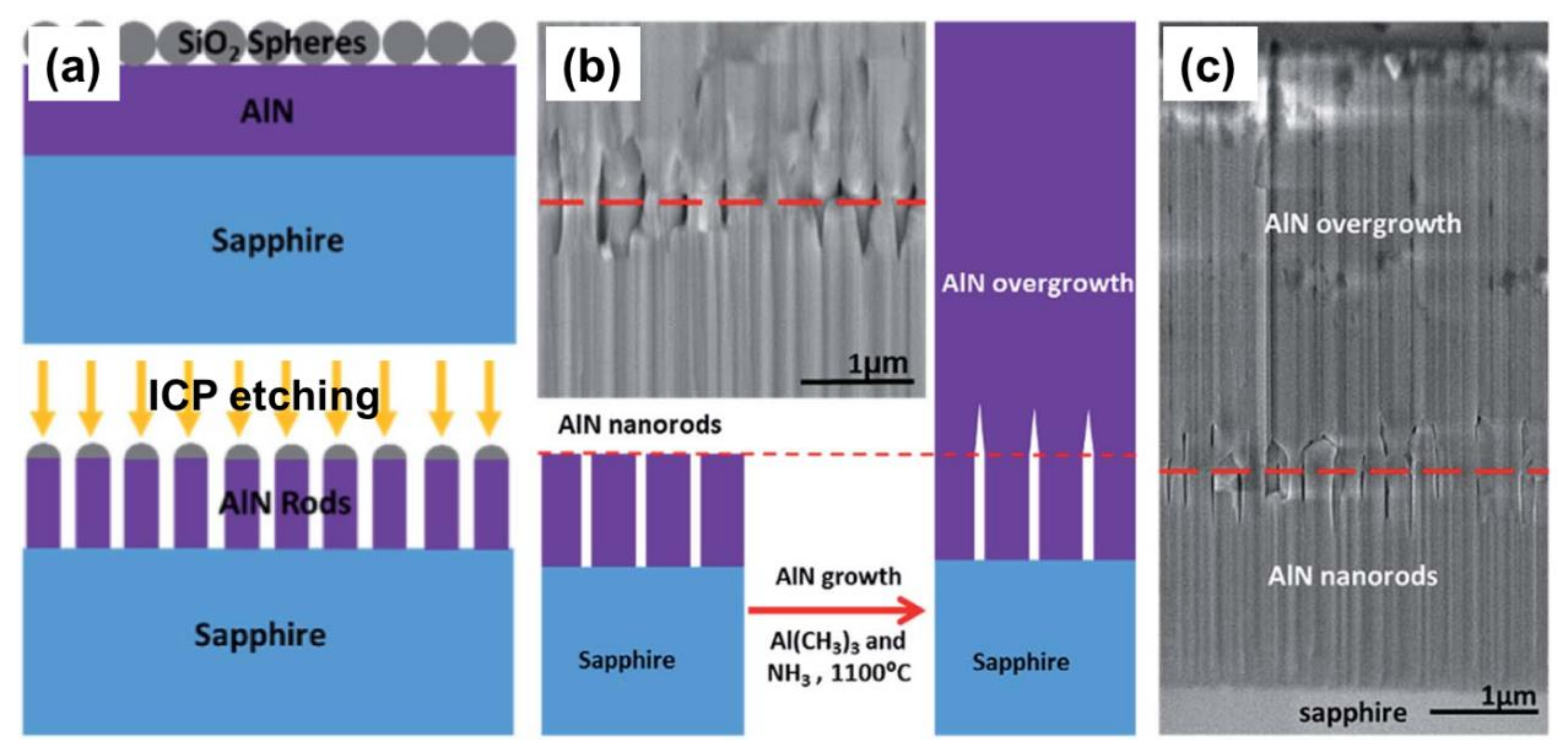
To address this issue, nanoscale ELOG was proposed, which benefits from the development of micro/nano processing technology. In 2013, P. Dong et al. reported 4 μm-thick ELOG-AlN grown on nano-patterned sapphire substrates (NPSS) using SiO2 nanosphere lithography [59]. The concave triangle cones had a diameter of 500 nm and a depth of 230 nm. The pattern period was 900 nm, which was determined by the diameter of the SiO2 nanospheres. Profiting from the greatly reduced pattern size, the coalescence thickness decreased to 3 μm, significantly thinner than those grown on conventional microscale patterned substrates. The RC FWHMs for (0002) and (10−12) reflections were 86.4 and 320.4 arc sec, respectively. This work opened up a new path for the ELOG of AlN. Then, ELOG of AlN on patterned AlN nanorods (diameter = 323 nm) prepared by SiO2 nanosphere lithography was also demonstrated, as shown in Figure 11 [60]. A TDD <3.5 × 108 cm−2 and a coalescence thickness <1.5 μm were achieved. Another group proved that AlN nanorods prepared by SiO2 nanosphere lithography could enhance the light output power (LOP) of AlGaN-based DUV LEDs by improving the internal quantum efficiency (IQE) and light extraction efficiency (LEE) [61]. It is noted that the ELOG of AlN on the above small-size AlN nanorods can be performed at a relatively low temperature of 1050–1100 °C, which is about 200 °C lower than the former reports about ELOG-AlN. Therefore, even the ordinary MOCVD is capable of conducting the ELOG of AlN on small-size nanorods.
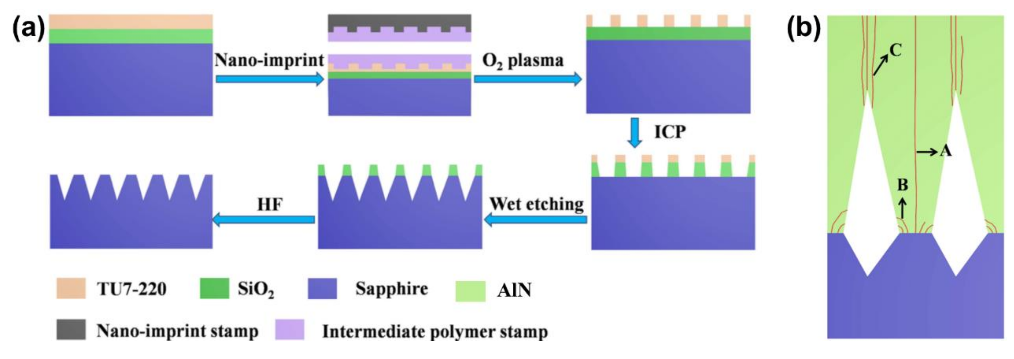
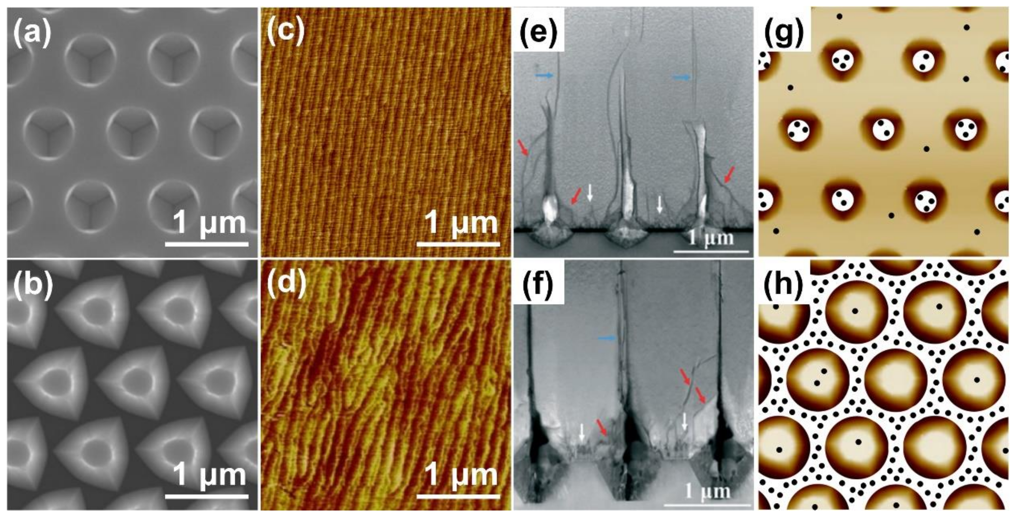
Despite these advantages, the SiO2 nanospheres easily form clusters, so the uniformity within wafer is poor. This problem can be solved by fabricating large-scale uniform hole-type NPSS by using nano-imprint technology. In 2016, L. Zhang et al. first applied this technology to the ELOG of AlN, as shown in Figure 12a [62]. The diameter of the concave cones was 650 nm, and the pattern period was 1 μm. Complete coalescence was achieved at less than 3 μm. Figure 12b displays that there are three competitive processes affecting the TDD of ELOG AlN on hole-type NPSS. Process A represents the vertical propagation process of dislocations generated on the unetched mesas, which undoubtedly contributes to the TDD of the top AlN layer. In process B, the image force makes the TDs near the side walls of AlN domains bend towards the free surfaces. These TDs will not reach the top AlN surface. Process C represents the process of new TDs generation around the coalescence boundaries, which largely depends on the misorientation angles between the adjacent AlN domains. The competitive results of these three processes are determined by the growth conditions and pattern configurations. For example, if we increase the diameter of the hole patterns, the area of the unetched mesas will decrease. Fewer dislocations will be generated in the initial growth stage, and most of these dislocations will go through process B rather than process A. Nevertheless, the increased misorientation angles between the adjacent AlN domains will result in the occurrence of process C with a high probability. Their follow-up research also proved that hole-type NPSS demonstrated lower TDD and surface roughness compared with pillar-type NPSS, despite that their pattern sizes were comparable, as shown in Figure 13 [63]. It is attributed to the big difference in the area ratio of coalescence zones. A smaller ratio of coalescence zones (hole-type NPSS) is more conductive to obtaining low-TDD and smooth AlN. By further optimizing the period size of hole-typ NPSS, the TDD can be reduced to 2.9 × 108 cm−2 [64].
Benefiting from low TDDs, UV LEDs fabricated on ELOG-AlN templates exhibit high light output power and high EQE, becoming one of the main technical routes. K. Nagamatsu et al. reported that the output power exhibited by a 355 nm UV LED fabricated on ELOG AlN template was 27 times higher than those on planar AlN templates [65]. H. Hirayama et al. reported maximum LOP of 2.7 mW under CW operation in a 273 nm DUV LED grown on conventional ELOG-AlN template [66]. LOP of 3.03 mW and EQE of 3.45% at 20 mA were achieved in a 282 nm DUV LED grown on NPSS by P. Dong et al. [59]. N. Susilo et al. reported LOP of 1.1 mW under CW operation at 20 mA in a 265 nm DUV LED on high-quality AlN templates fabricated by combining ELOG and high temperature annealing [67]. Although the ELOG technique has demonstrated great advantages in reducing TDD and improving device performance, it still needs to solve the problem of unevenly distributed stress, relatively high fabrication cost and poor repeatability. The unevenly distributed stress is attributed to the generation of tensile stress around the coalescence boundaries. The high cost results from the complicated fabricating processes of AlN, including lithography, etching, cleaning, growth, and even regrowth. Moreover, the thickness of AlN is usually >5 μm even for the ELOG-AlN grown on NPSS. The poor repeatability originates from the multiple fabricating processes those hard to be managed and the sensitiveness of AlN growth. These problems are expected to be solved when the NPSS is industrialized on a large scale.
3.4. High Temperature Annealing (HTA)
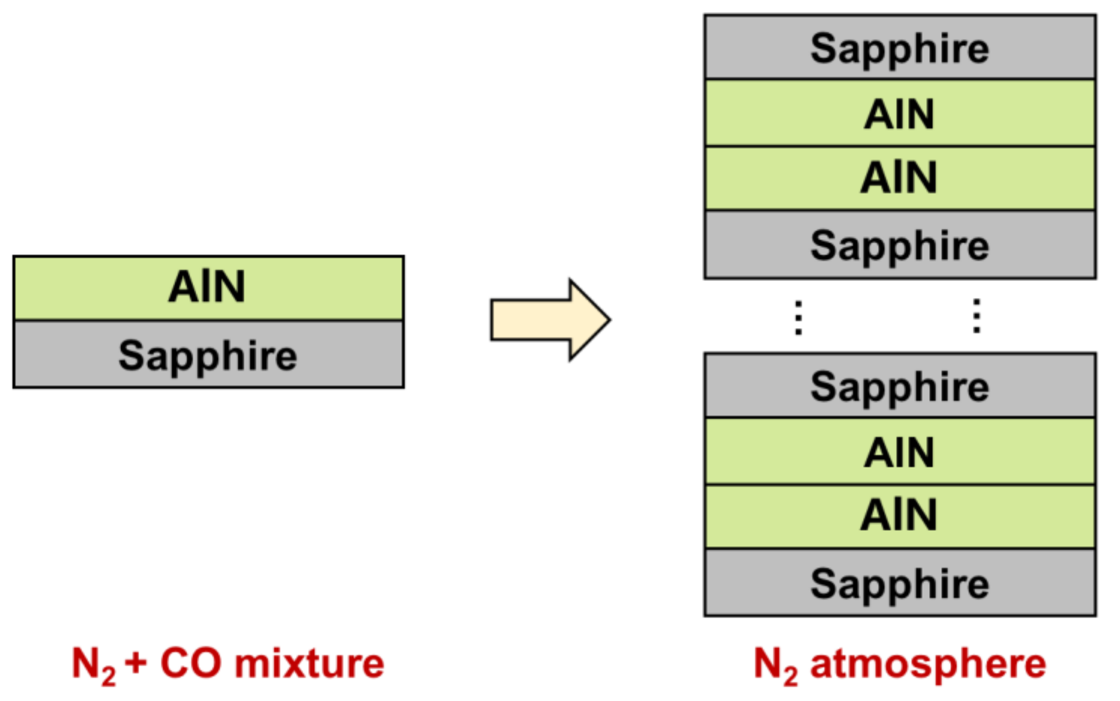
Although the traditional in situ epitaxial growth techniques including MSG and ELOG can achieve a relatively low TDD <5 × 107 cm−2, AlN layers with a thickness >5 μm are needed to enhance dislocation termination and annihilation. To realize TDD within a thinner AlN layer, ex situ high temperature annealing (HTA) was proposed. Actually, the annealing of AlN has been adopted and studied since 2005 [68], while efficient annealing temperatures were not reported until 2016 [69]. In that year, H. Miyake et al. reported the annealing result of a 300 nm-thick MOCVD-grown AlN buffer layer. The HTA was performed at 1650–1700 °C under N2-CO mixture for 1 h. After the regrowth of 2 μm-thick MOCVD-AlN on the 300 nm-thick annealed AlN epilayer, the FWHMs of (0002) and (10−12) plane X-ray rocking curves were reduced to 16 and 154 arcsec, respectively. The HTA technique thus started to show application prospect in improving crystalline quality. However, this annealing process needs the toxic CO with high partial pressure to suppress the decomposition of AlN at ultrahigh annealing temperature. To simplify annealing process, reduce experimental risk, and suppress the surface decomposition at high temperature, the concept of face-to-face annealing (FFA) with pure N2 atmosphere was proposed [70]. As shown in Figure 14, one AlN/sapphire wafer is placed on the other one, with two AlN surfaces in close contact with each other. One of the paired AlN/sapphire wafers can also be replaced by a bare sapphire substrate. If batch HTA processing is required, paired wafers can be continually stacked as long as the temperature uniformity is guaranteed. All these advantages have caused FFA with pure N2 atmosphere to become the mainstream HTA process. Research from many different groups is based on this framework.
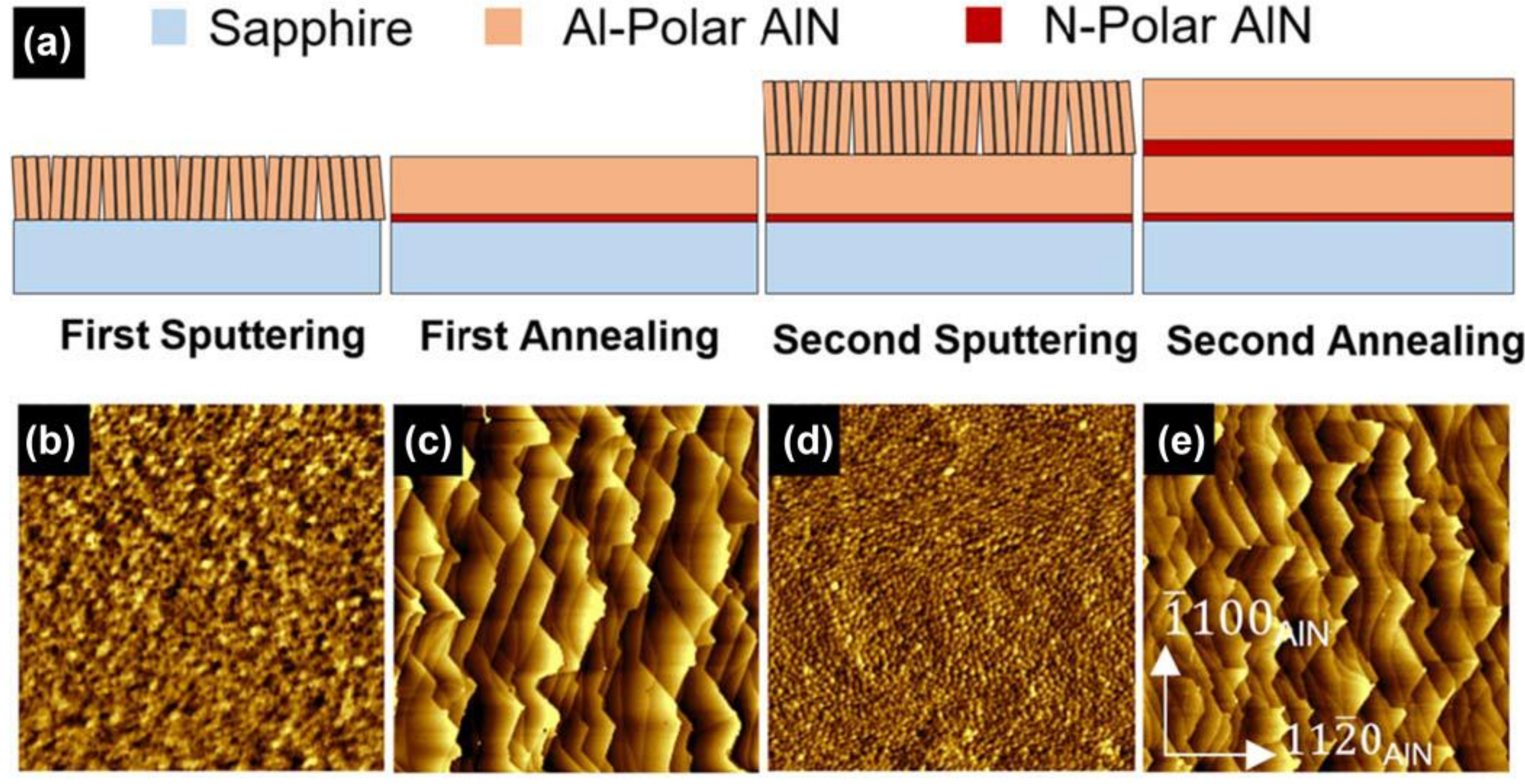
Generally, there are two main ways to prepare AlN/sapphire template for HTA. The first way is using radio-frequency (RF) magnetron sputtering, which enables the fabrication of large-scale and low-cost AlN layer with excellent c-axis orientation [17,47]. Chia-Yen Huang et al. demonstrated that a TDD lower than 5.0 × 108 cm−2 could be achieved by regrowing a 2.5 μm-thick MOCVD AlN layer on a 300 nm-thick annealed sputtered AlN buffer layer [71]. By optimizing the sputtering conditions, a lower TDD of 2.07 × 108 cm−2 was achieved in a 480 nm-thick sputtered AlN template after HTA and regrowth [72]. The mechanism of dislocation reduction is that the recrystallization of AlN at ultrahigh annealing temperature promotes the reduction of domain boundaries. When the annealing temperature is higher than 1700 °C, the domain boundaries may completely disappear as a result of gradual coalescence. After the coalescence of domain boundaries, lots of nano-voids form at the residual spaces between the original domain boundaries, and they distribute randomly in the AlN film. J. Ben et al. found that these nano-voids could block dislocations from spreading upwards [73]. It provides a new channel for dislocation termination, which is similar to the nano-void-induced dislocation blocking effect observed in our MSG-AlN sample [17,52]. The difference is the formation of nano-voids in MSG-AlN originates from the high lateral coverage speed and large depth/width ratio between adjacent 3D islands, while the formation of the nano-voids in HTA-AlN is ascribed to the coalescence of domain or the reaction between paired dislocations. Therefore, the nano-voids in MSG-AlN are slender in shape, but the nano-voids in HTA-AlN are hexagonal and dynamically changing due to the continuous dislocation absorption. Given that the conventional one-step and constant-temperature HTA process have some physical limitations, it is hard to achieve a TDD <108 cm−2. To further reduce the TDD, the AlN buffer used for HTA needs to be thickened. Thus, a double sputtering and annealing process (Figure 15) was developed to fabricate 1.2 μm-thick AlN template, which can avoid tensile stress accumulation and decrease the probability of cracking [74]. Inspired by the thermal cycle annealing (TCA) method for reducing the TDDs in GaAs, Ge, and PbSe grown on Si, Ding Wang et al. performed TCA on 800 nm-thick sputtered AlN buffer. The FWHMs for (0002) and (10−12) diffraction were decreased to 12 and 82 arcsec, corresponding to a TDD of ~8 × 107 cm−2 [75]. Due to the improved crystalline quality, N. Susilo reported that the 268 nm LEDs grown on 350 nm-thick sputtered and annealed AlN/sapphire templates showed a similar light output performance with those grown on ELOG AlN templates [76].
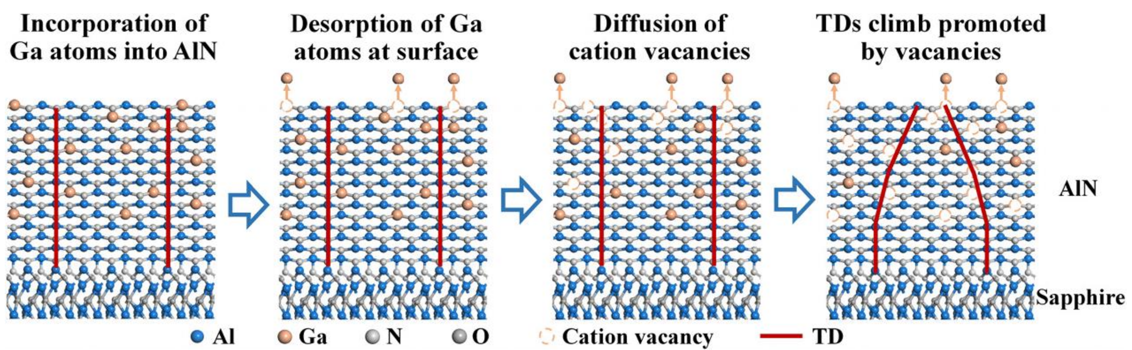
The second way to prepare an AlN/sapphire template for HTA is adopting MOCVD. The advantage of this way lies in that the regulation of AlN by MOCVD has higher freedom degree. M. X. Wang et al. reported HTA of a 540 nm-thick AlN films grown by MOCVD under N2 ambient. XRD FWHM values of 59 and 284 arcsec were achieved for (0002) and (10−12) diffractions, respectively [77]. They also found that AlN films grown on nitridation treated sapphire substrates exhibited lower TDDs after HTA process, compared with those grown on alumination-treated substrates [78]. It is verified that nitridation process before growth leads to the formation of higher-density AlN columns of smaller size, which can be easily rearranged during the HTA process. Obviously, although HTA can cause lattice rearrangement, the actual results largely depend on the AlN column distribution before HTA. To promote dislocation climbing and interaction within a thin layer, J. M. Wang et al. intentionally introduced supersaturated Ga vacancies (VGa) by inducing Ga desorption during the HTA process of Ga-doped AlN layer, as shown in Figure 16 [79]. The TDD was reduced to 1.58 × 108 cm−2, a reduction of one order of magnitude compared with conventional HTA methods. As result, a 280 nm AlGaN-based DUV LED fabricated on the HTA AlN templates obtained a light output power of 39.1 mW at 200 mA.
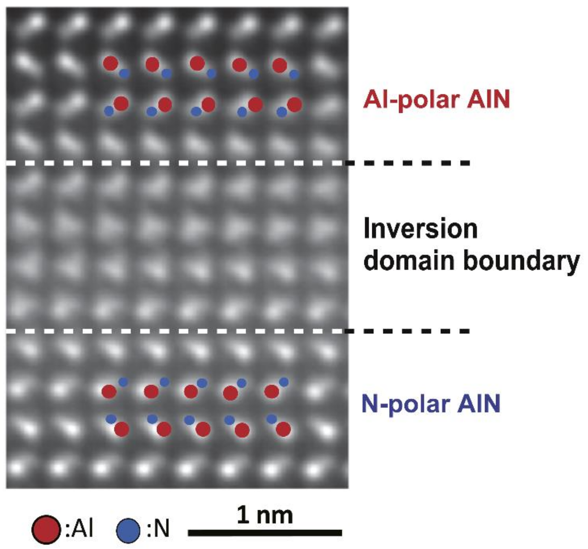
In addition to the improvement of crystalline quality, there is another common phenomenon. Inversion domains were found within tens of nanometers above the AlN/sapphire interface after HTA, in which polarity changes from N-polar to Al-polar along c-axis direction [80], as shown in Figure 17. DFT calculations indicate that polarity inversion is attributed to the formation of Al-vacancies, Al-Al bonds and Al-O bonds in the inversion region during HTA process. O impurity plays a very important role in this process. Inspired by this, Z. Liu et al. demonstrated the polarity of HTA AlN can be tuned by introducing trace oxygen in the initial sputtering process [81]. Pure N-polar AlN films were achieved by sputtering in pure N2 ambient and HTA afterwards, while the polarity would transmit to pure Al-polar when the supply time of trace oxygen exceeded 150 s. The FWHM values for (0002)/(10−12) directions reached 41.3/132.5 arcsec for N-polar and 38.2/158.7 arcsec for Al-polar. It provides a very useful method to obtain high-crystalline-quality N-polar AlN, which is very difficult for the in situ epitaxial growth techniques.
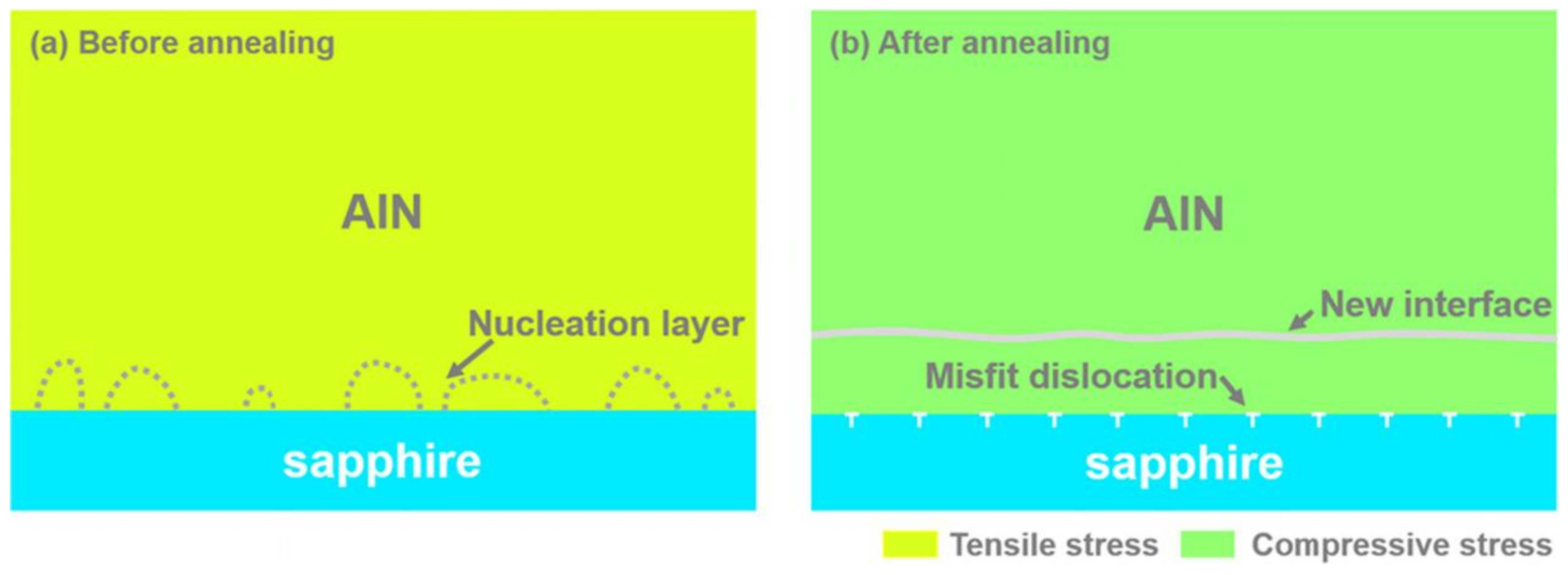
Although great progress has been achieved using the HTA technique, there are some existing problems that need to be solved such as strong residual stress, severe C impurity contamination and high-concentration point defects. The stress state of AlN epilayer achieved by HTA technique is quite different from that of the conventional AlN epilayer. As we know, AlN grown on sapphire substrate usually presents tensile stress, which originates from grain boundaries during the coalescence process. After the HTA process, the grain boundaries disappear due to the lattice rearrangement, meaning that the tensile stress is accordingly eliminated. The mismatch stress is completely released by generating periodic misfit dislocations lying in the AlN/sapphire interface, as shown in Figure 18. Therefore, the AlN epilayer is nearly stress-free at an annealing temperature such as 1700 °C. However, when the AlN/sapphire template is cooled down from the annealing temperature to room temperature/MOCVD growth temperature, the large thermal mismatch between AlN and sapphire results in strong residual compressive stress [82]. The compressive stress is as large as 1.3–1.5 GPa, which can be calculated based on the Raman spectra and thermal expansion coefficient [82,83]. The excess compressive stress may cause the deterioration of surface morphology, unwanted wafer bowing, and severe composition pulling effects, which should be controlled in a proper range [84,85,86,87,88]. Additionally, impurities from the graphite susceptor and chamber are easily incorporated into the AlN epilayer at the annealing temperature. At the same time, the high temperature also facilitates the formation of point defects. Therefore, regrowth is usually needed to reduce the concentrations of impurities and point defects. Despite this, the effect of impurities and point defects on the light absorption still exists, which may have an influence on the performance of optical and optoelectronic devices [89].
3.5. Quasi-Van der Waals Epitaxy (QvdWE)
Van der Waals epitaxy (vdWE) refers to epitaxial growth on layered or two-dimensional (2D) materials, wherein there is only weak Van der Waals interaction between epilayers and layered/2D materials. This character facilitates the exfoliation of epilayer from layered/2D material-coated substrate, thus providing great promise for the flexible and wearable electronic devices [90,91,92]. Due to the lack of dangling bonds on the top surfaces of h-BN and graphene, however, direct growth of AlN on perfect h-boron nitride (BN)/graphene results in porous surface and poor crystalline quality. To realize better surface morphology and crystalline quality, we need to destroy the perfect characteristics of h-BN/graphene and introduce a small amount of extra force in addition to Van der Waals interaction. Therefore, strictly speaking, epitaxial growth of AlN on h-BN/graphene should be defined as quasi-vdWE (QvdWE).
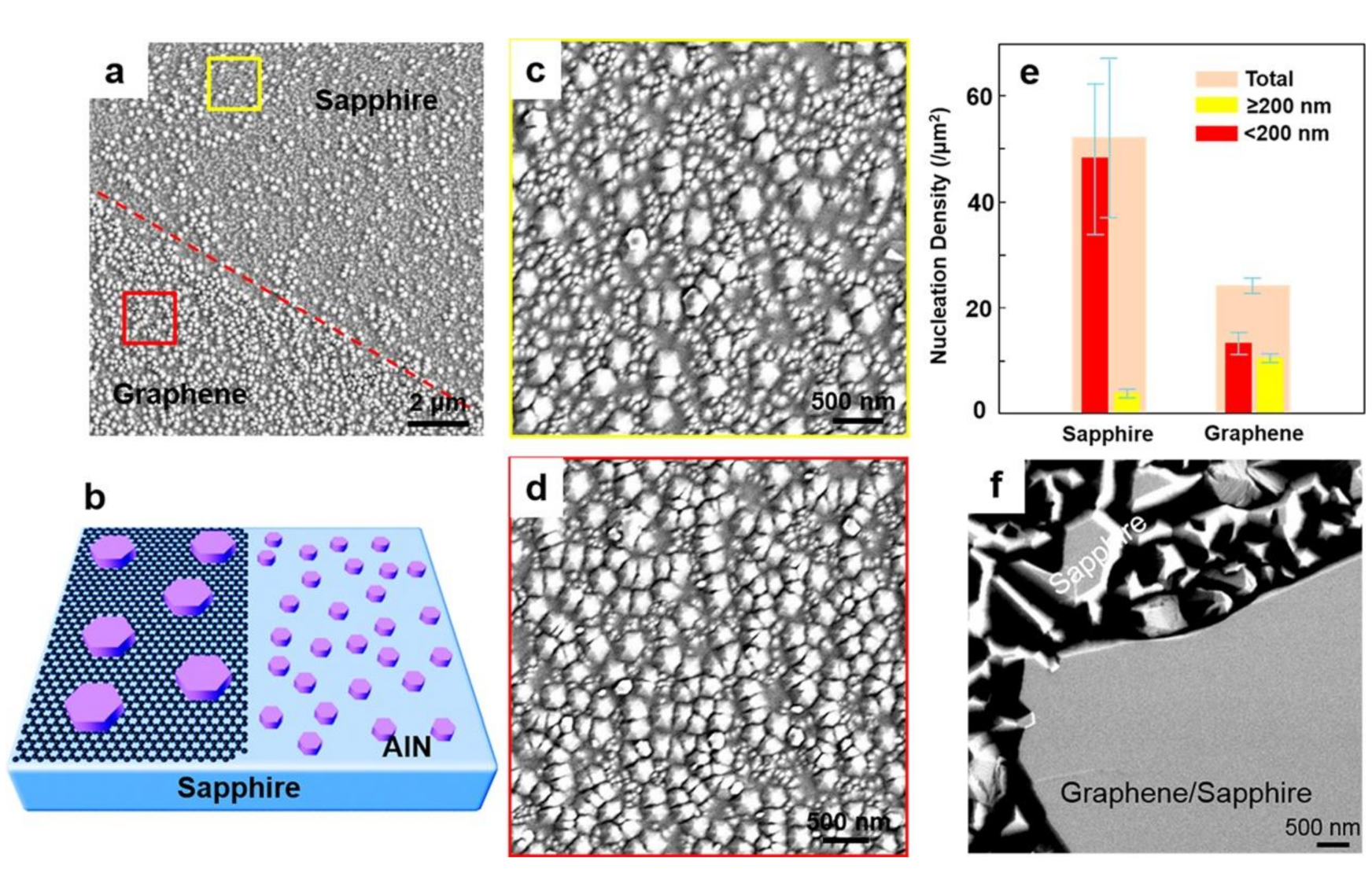
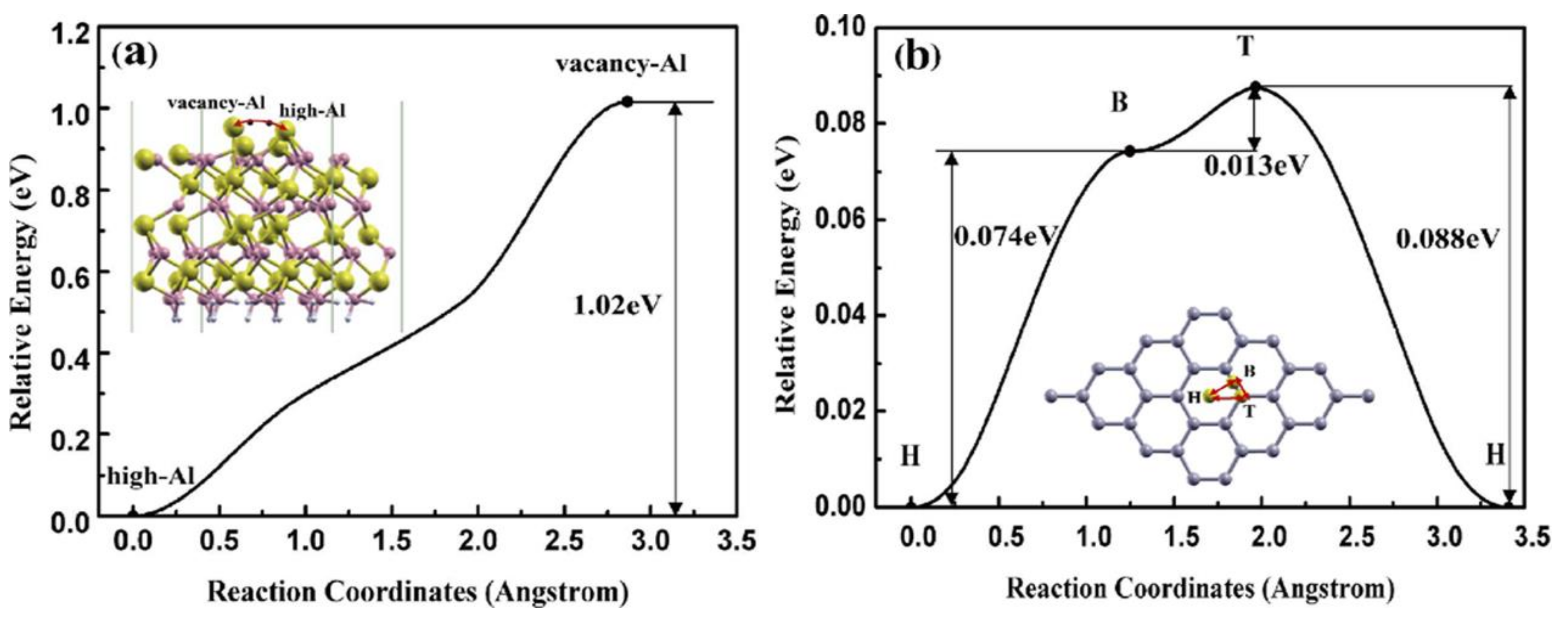
Generally, the transferred graphene sheet on sapphire substrate is not continuous and perfect. There are also rich dangling bonds at the graphene domain boundaries, and the graphene wrinkles can also increase the reactivity between graphene and the AlN epilayer. These imperfections can act as nucleation sites for AlN, although the nucleation sites are still sparse. It has been reported that the nucleation density of AlN on sapphire substrate is 41 μm−1, while that on graphene/sapphire hybrid substrate is only 23 μm−1, as shown in Figure 19 [93]. The lower nucleation density reduces the density of threading dislocations, which mainly formed at the coalescence boundaries of AlN islands. In the aspect of migration barrier, there is also a big difference. Figure 20 shows that the migration barrier of Al adatoms on the bare sapphire substrate is as high as 1.02 eV, while those between different sites (H, B, and T) of graphene are less than 0.1 eV [94]. It means that Al adatoms are very hard to migrate on bare sapphire surface even at a high growth temperature of 1200 °C, but they can migrate on the graphene surface nearly without obstacles. The better migration ability of Al adatoms on graphene surface enables the faster coalescence of AlN surface. In addition to the above advantages, the h-BN/graphene buffer can even screen the interaction between AlN and sapphire substrate, which significantly decreases the mismatch stress in the AlN epilayer.
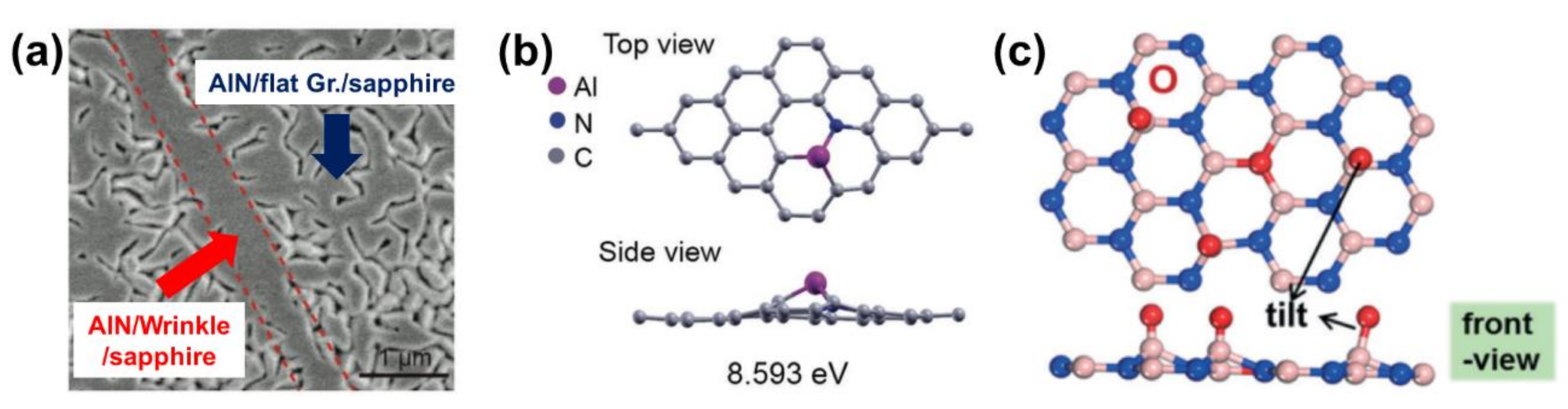
In some cases, more nucleation sites of AlN on graphene are needed. To realize this goal, we can intentionally introduce more imperfections. It has been reported that periodical graphene wrinkle arrays can be transferred onto sapphire substrate. The wrinkle density is as high as 10 μm−2, which effectively increases the nucleation sites of AlN. The increased nucleation sites and excellent lateral migration ability lead to a faster lateral coalescence rate, as shown in Figure 21a. As a result, the coalescence ratio of AlN significantly increases from 2.8% (flat graphene region) to 99.8% (graphene wrinkle region) after 6 min growth. In addition to introducing imperfections, N2/O2 plasma treatment is also adopted to realize N/O doping in h-BN/graphene, forming C-N/C-O/N-B-O bonding configurations that serve as nucleation sites for AlN epilayer [95,96]. At the nucleation sites, there is covalent bonding between AlN epilayer and impurity atoms, as shown in Figure 21b,c. These approaches enable the free control of nucleation site density.
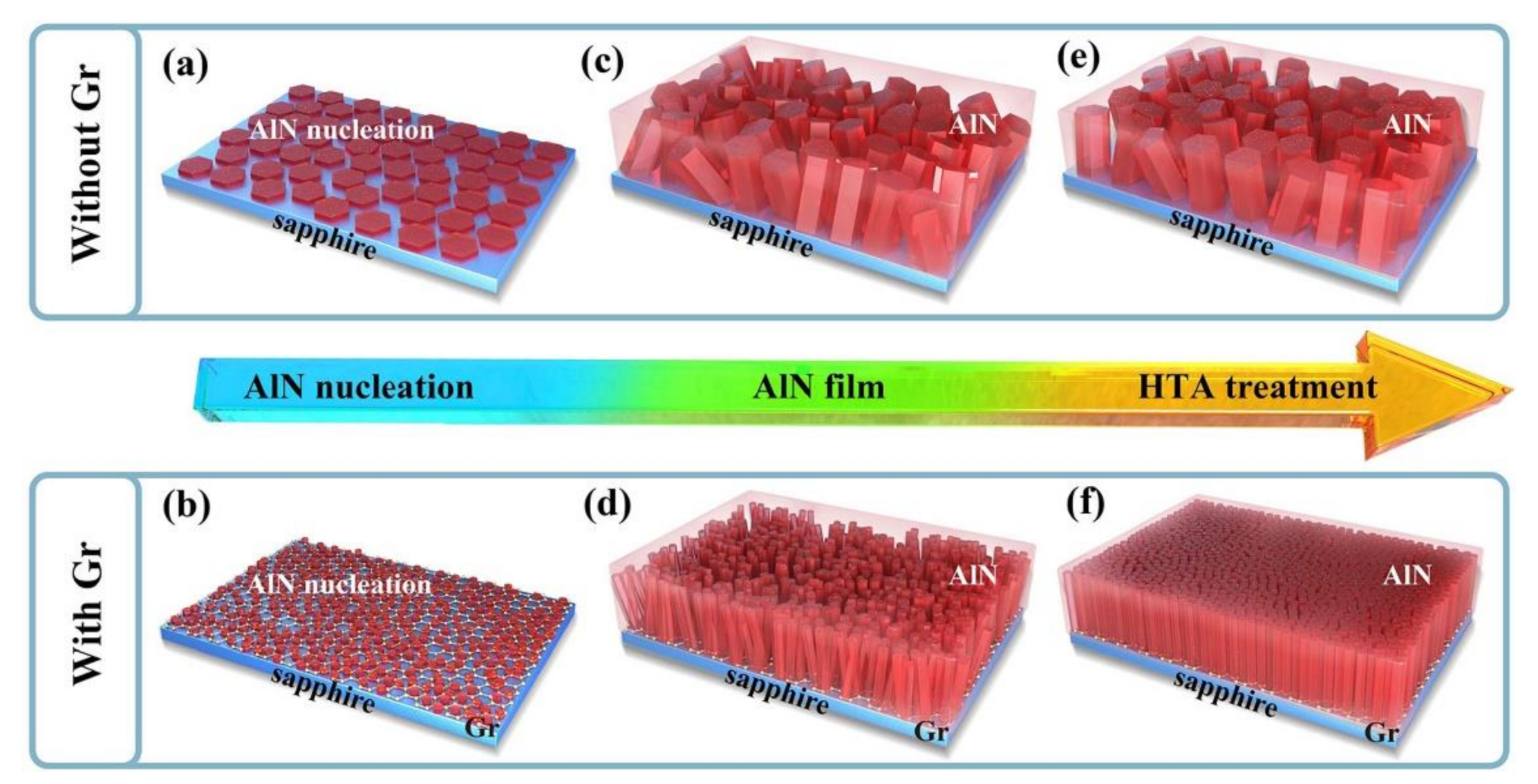
The QvdWE technique can also be combined with other growth techniques. It has been demonstrated that graphene facilitates the lateral coalescence of AlN grown on nano-patterned sapphire substrate (NPSS), which is always a tricky issue for ELOG technique. The fast lateral coalescence benefits from the excellent lateral migration ability of Al adatoms on graphene. For example, AlN grown on a 700 nm-wide and 400 nm-deep sapphire-inverted cone needs a thickness of 2.4 μm to realize the entire coalescence. By inserting a graphene buffer, however, the coalescence thickness is decreased to <1 μm, significantly reducing material and time cost. In addition, QvdWE technique is found to be good for the HTA [98]. By employing N2 plasma pretreatment on graphene/sapphire hybrid substrate, high-density and small-size AlN nucleation islands can be obtained. During the recrystallization process of HTA, those small-diameter AlN columns are easily rearranged, reducing the tilt and twist between different AlN columns, as shown in Figure 22. Therefore, the screw, edge, and mixed type threading dislocations are all decreased. Importantly, the graphene sheet can destroy the coherence between sapphire substrate and AlN epilayer, which usually results in strong biaxial compressive stress during the cooling down process of HTA. Thus, the AlN epilayer is nearly stress-free.
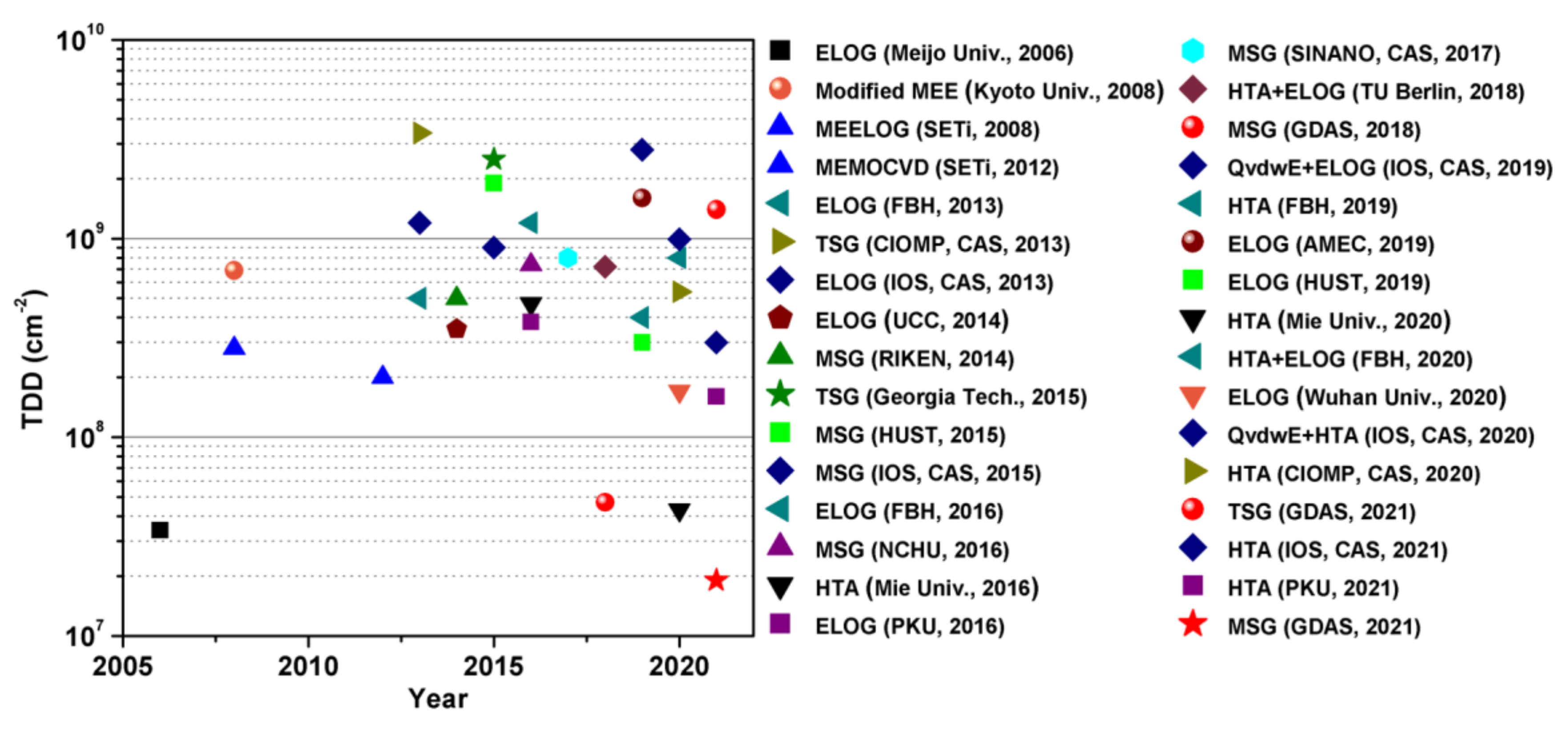
4. The TDD Compilation of AlN Films Grown by Different Techniques
Figure 23 summarizes the reported TDD values (2005–2021) of AlN films grown by different techniques. The laboratory level of TDD can be decreased to <5 × 107 cm−2 by using ELOG, HTA, and MSG growth techniques, and the industrialization level of TDD is decreased to 108–109 cm−2.
It is noted that there has been no unified standard for the evaluation of TDD. X-ray rocking curve (XRC) scan is the most common method to evaluate TDD. However, X-ray has a large penetration depth in AlN material, meaning that the measurement result containing the information of the whole AlN epilayer rather than that of the top AlN epilayer [110]. Thus, the TDD of the top AlN epilayer extracted from XRC scan is usually overestimated, especially when the TDD is low. Cross-sectional TEM and plan-view TEM results can give the TDD of the top AlN layer, as shown in Figure 24. Nevertheless, they have certain degrees of randomness, since the measurement area is usually <50 μm2 [17,53,74]. Plan-view cathodoluminescence (CL) spectroscopy, which is frequently used to count the TDD of GaN epilayer, is no longer applicable to AlN because of the poor conductivity of AlN and the weak responsivity of the detector at ~200 nm. The TDD evaluated by etch pit density is also inaccurate when the AlN surface is under etched or over etched [111]. Additionally, even if the measurement method is the same, different equipment may obtain different results. Therefore, strictly speaking, the TDD results from different groups or evaluated by different methods should not be directly compared. Here, we list some representative TDD values to see the general development trend.
5. Thermal Conductivity Control of AlN
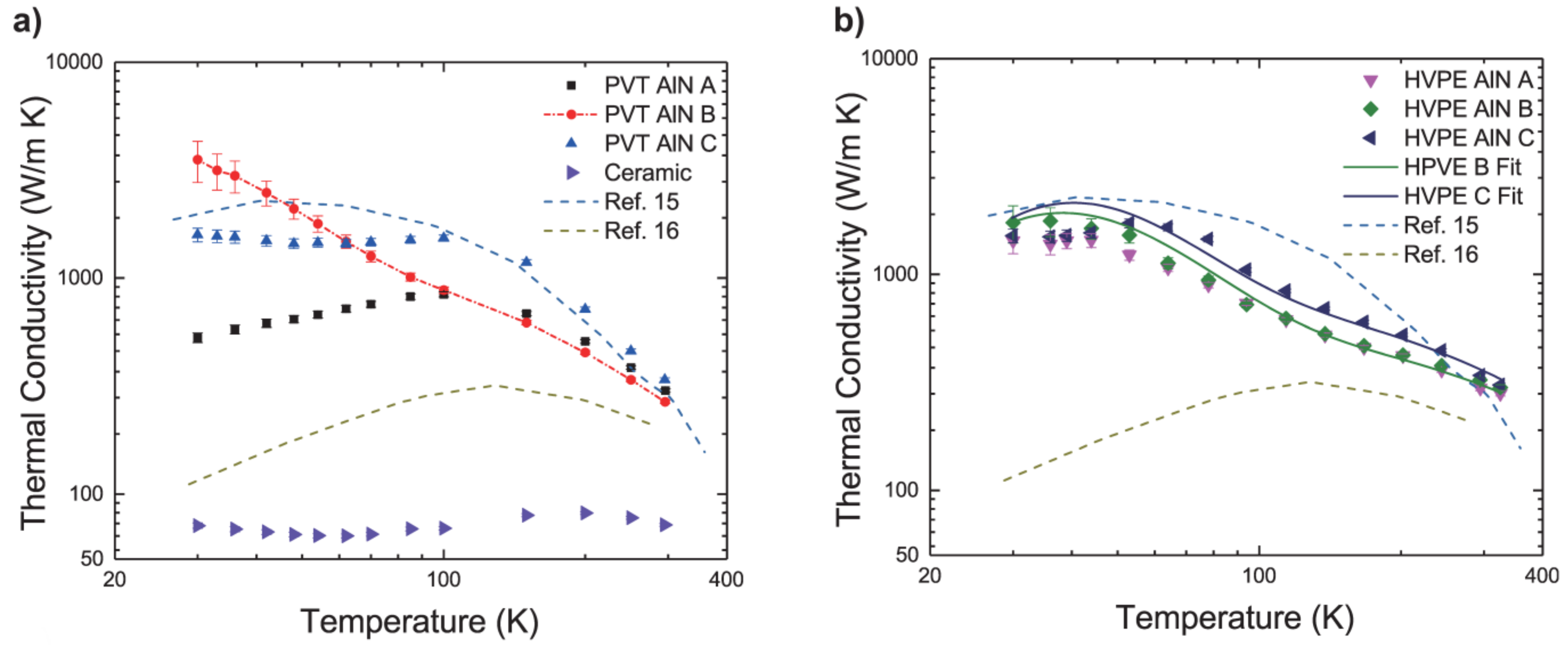
As a substrate/template, AlN has superior thermal conductivity in theory (320 W/m·K), which is favored by next-generation optoelectronic and electronic devices such as high-power UV LEDs, LDs, PDs, and HEMTs. In most cases, however, the measured thermal conductivities of AlN are far less than the calculated intrinsic thermal conductivity. Point defects, stacking faults, misfit and threading dislocations, grain boundaries, impurities, and their complexes are responsible for this. As we know, thermal conductivity in non-metallic solids is affected by the intrinsic and extrinsic phonon scattering rates. The intrinsic normal and Umklapp scattering processes depend on the crystal system, while the extrinsic scattering is related to defects, impurities, and their complexes. Due to the ultralow TDD values and the absence of grain boundaries, bulk AlN wafers generally have higher thermal conductivities. However, R. Rounds et al. found that the bulk thermal conductivity of PVT single-crystal AlN showed significant variation from 268 to 339 W/m·K at 325 K, depending on the impurity and point defect concentrations, as shown in Figure 25 [112]. At low temperature, the difference was even magnified to one order of magnitude because phonon scattering by point defects dominated at this time. This means point defects play a very important role in determining the thermal conductivity of AlN.
As for AlN films grown on sapphire substrates, achieving high thermal conductivity is more difficult because of the poor crystalline quality. Until 2020, Z. Cheng et al. reported high cross-plane thermal conductivity observed in AlN/sapphire template [113]. They improved the crystalline quality of AlN/sapphire by introducing air-voids near the AlN/sapphire interface, which allowed for the growth of high-quality and crack-free AlN films with a thickness >15 μm. The physical thought is similar to that which we mentioned in the MSG growth technique section [114,115]. Meanwhile, the high growth temperature and high-purity precursors effectively suppressed the incorporation of impurities such as O and C. As a result, the TDD values were estimated to be ~(1–3) × 108 cm−2 by counting etching pit densities. Although the TDD values of the thick AlN/sapphire templates were several orders of magnitude higher than those of the commercial PVT bulk AlN, the TDD level of (1–3) × 108 cm−2 were thought to have a weak influence on the thermal conductivity, especially for cross-plane thermal conductivity. Secondary-ion mass spectrometry (SIMS) results showed that the impurity concentrations in the thick AlN/sapphire templates were 1–2 orders of magnitude lower than those in the commercial PVT bulk AlN. By fitting temperature-dependent thermal conductivity data, the vacancy concentrations in the thick AlN/sapphire templates were considered negligible, while those in the commercial PVT bulk AlN reached 1019–1020 cm−3. Therefore, the low impurity and vacancy concentrations in the thick AlN/sapphire templates led to a high thermal conductivity of 321 W/m·K at 300 K, which is consistent with the density functional theory (DFT) calculation results of perfect bulk AlN. In comparison, those of the commercial PVT bulk AlN were only 216 and 278 W/m·K at 300 K.
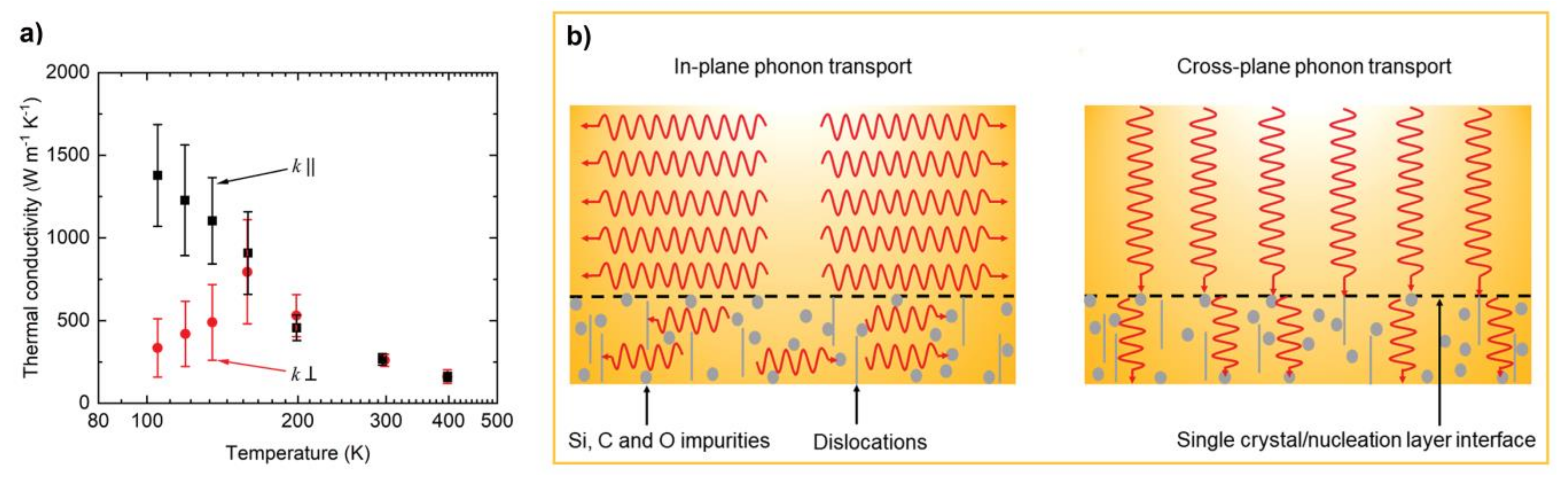
In 2021, they also reported AlN/sapphire templates with high in-plane thermal conductivity of (260 ± 40) W/m·K at 300 K, despite the fact that the thickness of the AlN films was only 3–6 μm [116]. By comparing the in-plane (k‖) and cross-plane (k⊥) thermal conductivities at different temperatures, they found that there was anisotropy in the thermal conductivity of AlN/sapphire templates below 160 K, as shown in Figure 26a. They proposed a simplified physical model, assuming that there was a single crystal/nucleation layer interface. Figure 26b shows that in-plane phonon travels nearly freely given that the vertical threading dislocations are relatively rare, while the cross-plane phonon suffers from severe interface scattering. At high temperature, the phonon–phonon scattering was more prominent compared with phonon–interface scattering, so the in-plane (k‖) and cross-plane (k⊥) thermal conductivities were nearly the same. At low temperature, the phonon–phonon scattering effect was weakened and the phonon–interface scattering dominated, resulting in the severe thermal conductivity anisotropy.
6. Future Challenges
The above review focuses on the recent advances in AlN as templates. In the near future, AlN may act as a real semiconductor if efficient n-type and p-type doping with good reproducibility are achieved. For n-type doping, silicon (Si) is a commonly used donor in III-nitrides. However, unlike Si impurity in GaN and Ga-rich AlGaN, it is no longer a shallow donor in Al-rich AlGaN and AlN. The activation energies of Si donors range from 78 to 345 meV [117]. Moreover, the carrier concentration decreases with the increase in Si doping concentration in the high doping regime, i.e., the compensation knee. It is considered to be related to DX transition, cation vacancies, SiN, and VAl-SiN complexes, preventing the achievement of high carrier concentration [117]. In addition, since the efficient p-type doping still remains an obstacle in Al-rich AlGaN nowadays, p-type doping of AlN is definitely more challenging. It suffers from larger acceptor activation energy (~500–780 meV) [118,119,120], lower solid solubility of dopants [121], high-level compensation by defects and impurities [122].
Recently, there has been some new progress on the n-type and p-type doping of AlN. M. H. Breckenridge et al. achieved a high n-type conductivity (>1 Ω−1 cm−1) and carrier concentration (5 × 1018 cm−3) at room temperature. They realized Si doping of homoepitaxial AlN by combining ion implantation and non-equilibrium annealing process at relatively low temperature (1200 °C). A defect Quasi Fermi Level (dQFL) control method was adopted to suppress self-compensation [123]. H. Ahmad et al. reported a record-high bulk hole concentration of 3.1 × 1018 cm−3 in a beryllium-doped AlN/sapphire via metal modulated epitaxy (MME) in an MBE system [124]. Despite this progress, more research work about n-type and p-type doping of AlN is needed to make it a really useful semiconductor.
In the short term, AlN films grown on sapphire substrates still have obvious advantages over bulk AlN such as large size, low cost, and excellent UV transparency. In the future, however, the size, cost, and transparency problems of bulk AlN are expected to be gradually alleviated. To maintain their advantages in industrial application, AlN films grown on sapphire substrate must further improve its crystalline quality and reduce its cost. Therefore, characteristics including low TDD, controllable doping, low impurity concentration, low point defect concentration, weak residual stress, thin layer, and a simple fabricating process need to be simultaneously satisfied. At present, all the AlN/sapphire growth techniques still have various problems. It is hard to determine which technique will be the mainstream in the future. We believe the ultimate growth technology should be integrated the advantages of various existing technologies.
7. Conclusions
Wurtzite AlN has many excellent properties including high electron mobility, high breakdown voltage, high piezoelectric coefficient, high thermal conductivity, high hardness, high corrosion resistance, high chemical and thermal stability, high bulk acoustic wave velocity, prominent second-order optical nonlinearity, as well as excellent UV transparency. Therefore, they are suitable for fabricating high-performance electronic, optoelectronic, optical, and acoustic devices. This article reviews the recent advances in fabricating wurtzite AlN film on (0001)-plane sapphire substrate. Benefiting from the fast development of growth technique and equipment, the crystalline quality of AlN has been significantly improved. The laboratory level of TDD can be decreased to <5 × 107 cm−2 by using ELOG, HTA, and MSG growth techniques. However, this is not enough to meet the demands of large-scale industrial applications. In the future, AlN/sapphire template must further improve its crystalline quality and reduce its cost to maintain its advantages over bulk AlN.
Author Contributions
Conceptualization, H.W., C.H. and W.Z. and Z.C.; methodology, H.W., L.H. and Q.W.; software, H.W., L.H. and Q.W.; validation, C.H., W.Z. and Z.C.; formal analysis, H.W., L.H. and Q.W.; investigation, H.W., L.H. and Q.W.; resources, H.W., L.H. and Q.W.; data curation, H.W., L.H. and Q.W.; writing—original draft preparation, H.W., C.H. and Z.C.; writing—review and editing, H.W., K.Z., C.H., L.H., Q.W., W.Z. and Z.C.; visualization, H.W., L.H. and Q.W.; supervision, C.H. and Z.C.; project administration, C.H. and Z.C.; funding acquisition, H.W., K.Z., C.H., L.H., Q.W., W.Z. and Z.C. All authors have read and agreed to the published version of the manuscript.
Funding
This work is supported by National Natural Science Foundation of China (Nos. 61804034, 62104048 and 62175043), Key-Area Research and Development Project of Guangdong Province (No. 2020B010172001), Key Area R&D Program of Guangzhou (No. 202103030002), Guangdong Basic and Applied Basic Research Foundation (Nos. 2021A1515012188 and 2019A1515110257), GDAS’ Project of Science and Technology Development (Nos. 2020GDASYL-20200104031 and 2018GDASCX-0112), Guangzhou Basic and Applied Basic Research Foundation (No. 202002030163).
Institutional Review Board Statement
Not applicable.
Informed Consent Statement
Not applicable.
Data Availability Statement
The data presented in this study are available on request from the corresponding author.
Conflicts of Interest
The authors declare no conflict of interest.
References
- Kneissl, M.; Rass, J. III-Nitride Ultraviolet Emitters; Springer: Berlin/Heidelberg, Germany, 2016. [Google Scholar]
- Yu, R.; Liu, G.; Wang, G.; Chen, C.; Xu, M.; Zhou, H.; Wang, T.; Yu, J.; Zhao, G.; Zhang, L. Ultrawide-bandgap semiconductor AlN crystals: Growth and applications. J. Mater. Chem. C 2021, 9, 1852–1873. [Google Scholar] [CrossRef]
- Tsao, J.; Chowdhury, S.; Hollis, M.; Jena, D.; Johnson, N.; Jones, K.; Kaplar, R.; Rajan, S.; Van de Walle, C.; Bellotti, E. Ultrawide-bandgap semiconductors: Research opportunities and challenges. Adv. Electron. Mater. 2018, 4, 1600501. [Google Scholar] [CrossRef] [Green Version]
- Fei, C.; Liu, X.; Zhu, B.; Li, D.; Yang, X.; Yang, Y.; Zhou, Q. AlN piezoelectric thin films for energy harvesting and acoustic devices. Nano Energy 2018, 51, 146–161. [Google Scholar] [CrossRef]
- Ni, X.; Fan, Q.; Hua, B.; Sun, P.; Cai, Z.; Wang, H.-C.; Huang, C.; Gu, X. Improvement of AlN Material Quality by High-Temperature Annealing Toward Power Diodes. IEEE T. Electron. Dev. 2020, 67, 3988–3991. [Google Scholar] [CrossRef]
- Chu, Y.; Kharel, P.; Yoon, T.; Frunzio, L.; Rakich, P.T.; Schoelkopf, R.J. Creation and control of multi-phonon Fock states in a bulk acoustic-wave resonator. Nature 2018, 563, 666–670. [Google Scholar] [CrossRef] [PubMed]
- Wang, W.; Mayrhofer, P.M.; He, X.; Gillinger, M.; Ye, Z.; Wang, X.; Bittner, A.; Schmid, U.; Luo, J. High performance AlScN thin film based surface acoustic wave devices with large electromechanical coupling coefficient. Appl. Phys. Lett. 2014, 105, 133502. [Google Scholar] [CrossRef]
- Jung, H.; Xiong, C.; Fong, K.Y.; Zhang, X.; Tang, H.X. Optical frequency comb generation from aluminum nitride microring resonator. Opt. Lett. 2013, 38, 2810–2813. [Google Scholar] [CrossRef] [Green Version]
- Liu, X.; Bruch, A.W.; Gong, Z.; Lu, J.; Surya, J.B.; Zhang, L.; Wang, J.; Yan, J.; Tang, H.X. Ultra-high-Q UV microring resonators based on a single-crystalline AlN platform. Optica 2018, 5, 1279–1282. [Google Scholar] [CrossRef] [Green Version]
- Kneissl, M.; Seong, T.-Y.; Han, J.; Amano, H. The emergence and prospects of deep-ultraviolet light-emitting diode technologies. Nat. Photonics 2019, 13, 233–244. [Google Scholar] [CrossRef]
- Wu, H.; Wu, W.; Zhang, H.; Chen, Y.; Wu, Z.; Wang, G.; Jiang, H. All AlGaN epitaxial structure solar-blind avalanche photodiodes with high efficiency and high gain. Appl. Phys. Express 2016, 9, 52103. [Google Scholar] [CrossRef]
- Zhang, Z.; Kushimoto, M.; Sakai, T.; Sugiyama, N.; Schowalter, L.J.; Sasaoka, C.; Amano, H. A 271.8 nm deep-ultraviolet laser diode for room temperature operation. Appl. Phys. Express 2019, 12, 124003. [Google Scholar] [CrossRef]
- Mackey, T.K.; Contreras, J.T.; Liang, B.A. The Minamata Convention on Mercury: Attempting to address the global controversy of dental amalgam use and mercury waste disposal. Sci. Total Environ. 2014, 472, 125–129. [Google Scholar] [CrossRef] [PubMed]
- Liu, S.; Luo, W.; Li, D.; Yuan, Y.; Tong, W.; Kang, J.; Wang, Y.; Li, D.; Rong, X.; Wang, T. Sec-Eliminating the SARS-CoV-2 by AlGaN Based High Power Deep Ultraviolet Light Source. Adv. Funct. Mater. 2021, 31, 2008452. [Google Scholar] [CrossRef] [PubMed]
- Li, D.; Jiang, K.; Sun, X.; Guo, C. AlGaN photonics: Recent advances in materials and ultraviolet devices. Adv. Opt. Photonics 2018, 10, 43–110. [Google Scholar] [CrossRef]
- Wang, Q.; Lei, D.; He, G.; Gong, J.; Huang, J.; Wu, J. Characterization of 60 mm AlN Single Crystal Wafers Grown by the Physical Vapor Transport Method. Phys. Status Solidi A 2019, 216, 1900118. [Google Scholar] [CrossRef]
- He, C.; Zhao, W.; Wu, H.; Zhang, S.; Zhang, K.; He, L.; Liu, N.; Chen, Z.; Shen, B. High-quality AlN film grown on sputtered AlN/sapphire via growth-mode modification. Cryst. Growth Des. 2018, 18, 6816–6823. [Google Scholar] [CrossRef]
- Shen, J.; Yang, X.; Liu, D.; Cai, Z.; Wei, L.; Xie, N.; Xu, F.; Tang, N.; Wang, X.; Ge, W. High quality AlN film grown on a nano-concave-circle patterned Si substrate with an AlN seed layer. Appl. Phys. Lett. 2020, 117, 22103. [Google Scholar] [CrossRef]
- Zollner, C.J.; Almogbel, A.; Yao, Y.; SaifAddin, B.K.; Wu, F.; Iza, M.; DenBaars, S.P.; Speck, J.S.; Nakamura, S. Reduced dislocation density and residual tension in AlN grown on SiC by metalorganic chemical vapor deposition. Appl. Phys. Lett. 2019, 115, 161101. [Google Scholar] [CrossRef]
- Ambacher, O.; Smart, J.; Shealy, J.; Weimann, N.; Chu, K.; Murphy, M.; Schaff, W.; Eastman, L.; Dimitrov, R.; Wittmer, L. Two-dimensional electron gases induced by spontaneous and piezoelectric polarization charges in N-and Ga-face AlGaN/GaN heterostructures. J. Appl. Phys. 1999, 85, 3222–3233. [Google Scholar] [CrossRef] [Green Version]
- Guo, W.; Sun, H.; Torre, B.; Li, J.; Sheikhi, M.; Jiang, J.; Li, H.; Guo, S.; Li, K.H.; Lin, R. Lateral-polarity structure of AlGaN quantum wells: A promising approach to enhancing the ultraviolet luminescence. Adv. Funct. Mater. 2018, 28, 1802395. [Google Scholar] [CrossRef]
- Ito, T.; Sakamoto, R.; Isono, T.; Yao, Y.; Ishikawa, Y.; Okada, N.; Tadatomo, K. Growth and Characterization of Nitrogen-Polar AlGaN/AlN Heterostructure for High-Electron-Mobility Transistor. Phys. Status Solidi. B 2020, 257, 1900589. [Google Scholar] [CrossRef]
- Kirste, R.; Mita, S.; Hussey, L.; Hoffmann, M.P.; Guo, W.; Bryan, I.; Bryan, Z.; Tweedie, J.; Xie, J.; Gerhold, M. Polarity control and growth of lateral polarity structures in AlN. Appl. Phys. Lett. 2013, 102, 181913. [Google Scholar] [CrossRef]
- Lemettinen, J.; Okumura, H.; Kim, I.; Rudzinski, M.; Grzonka, J.; Palacios, T.; Suihkonen, S. MOVPE growth of nitrogen-and aluminum-polar AlN on 4H-SiC. J. Cryst. Growth 2018, 487, 50–56. [Google Scholar] [CrossRef] [Green Version]
- Eom, D.; Kim, J.; Lee, K.; Jeon, M.; Heo, C.; Pyeon, J.; Nam, O. AlN nanostructures fabricated on a vicinal sapphire (0001) substrate. Cryst. Growth Des. 2015, 15, 1242–1248. [Google Scholar] [CrossRef]
- Akiyama, T.; Saito, Y.; Nakamura, K.; Ito, T. Nitridation of Al2O3 surfaces: Chemical and structural change triggered by oxygen desorption. Phys. Rev. Lett. 2013, 110, 26101. [Google Scholar] [CrossRef] [PubMed]
- McCauley, J.W.; Patel, P.; Chen, M.; Gilde, G.; Strassburger, E.; Paliwal, B.; Ramesh, K.; Dandekar, D.P. AlON: A brief history of its emergence and evolution. J. Eur. Ceram. Soc. 2009, 29, 223–236. [Google Scholar] [CrossRef]
- Sun, H.; Wu, F.; Park, Y.J.; Al Tahtamouni, T.; Li, K.-H.; Alfaraj, N.; Detchprohm, T.; Dupuis, R.D.; Li, X. Influence of TMAl preflow on AlN epitaxy on sapphire. Appl. Phys. Lett. 2017, 110, 192106. [Google Scholar] [CrossRef] [Green Version]
- Wang, J.; Xu, F.; He, C.; Zhang, L.; Lu, L.; Wang, X.; Qin, Z.; Shen, B. High quality AlN epilayers grown on nitrided sapphire by metal organic chemical vapor deposition. Sci. Rep. 2017, 7, 42747. [Google Scholar] [CrossRef] [Green Version]
- Miyagawa, R.; Yang, S.; Miyake, H.; Hiramatsu, K.; Kuwahara, T.; Mitsuhara, M.; Kuwano, N. Microstructure of AlN grown on a nucleation layer on a sapphire substrate. Appl. Phys. Express 2012, 5, 25501. [Google Scholar] [CrossRef]
- Mohn, S.; Stolyarchuk, N.; Markurt, T.; Kirste, R.; Hoffmann, M.P.; Collazo, R.; Courville, A.; Di Felice, R.; Sitar, Z.; Vennéguès, P. Polarity control in group-III nitrides beyond pragmatism. Phys. Rev. Appl. 2016, 5, 54004. [Google Scholar] [CrossRef] [Green Version]
- Funato, M.; Shibaoka, M.; Kawakami, Y. Heteroepitaxy mechanisms of AlN on nitridated c-and a-plane sapphire substrates. J. Appl. Phys. 2017, 121, 85304. [Google Scholar] [CrossRef]
- Ban, K.; Yamamoto, J.-I.; Takeda, K.; Ide, K.; Iwaya, M.; Takeuchi, T.; Kamiyama, S.; Akasaki, I.; Amano, H. Internal quantum efficiency of whole-composition-range AlGaN multiquantum wells. Appl. Phys. Express 2011, 4, 52101. [Google Scholar] [CrossRef]
- Reddy, P.; Hayden Breckenridge, M.; Guo, Q.; Klump, A.; Khachariya, D.; Pavlidis, S.; Mecouch, W.; Mita, S.; Moody, B.; Tweedie, J. High gain, large area, and solar blind avalanche photodiodes based on Al-rich AlGaN grown on AlN substrates. Appl. Phys. Lett. 2020, 116, 81101. [Google Scholar] [CrossRef]
- Zhang, J.; Wang, H.; Sun, W.; Adivarahan, V.; Wu, S.; Chitnis, A.; Chen, C.; Shatalov, M.; Kuokstis, E.; Yang, J. High-quality AlGaN layers over pulsed atomic-layer epitaxially grown AlN templates for deep ultraviolet light-emitting diodes. J. Electron. Mater. 2003, 32, 364–370. [Google Scholar] [CrossRef]
- Banal, R.G.; Funato, M.; Kawakami, Y. Initial nucleation of AlN grown directly on sapphire substrates by metal-organic vapor phase epitaxy. Appl. Phys. Lett. 2008, 92, 241905. [Google Scholar] [CrossRef] [Green Version]
- Zhang, J.; Hu, X.; Lunev, A.; Deng, J.; Bilenko, Y.; Katona, T.M.; Shur, M.S.; Gaska, R.; Khan, M.A. AlGaN deep-ultraviolet light-emitting diodes. Jpn. J. Appl. Phys. 2005, 44, 7250. [Google Scholar] [CrossRef]
- Tian, W.; Yan, W.; Dai, J.; Li, S.; Tian, Y.; Hui, X.; Zhang, J.; Fang, Y.; Wu, Z.; Chen, C. Effect of growth temperature of an AlN intermediate layer on the growth mode of AlN grown by MOCVD. J. Phys. D Appl. Phys. 2013, 46, 65303. [Google Scholar] [CrossRef]
- Wu, H.; Wang, H.; Chen, Y.; Zhang, L.; Chen, Z.; Wu, Z.; Wang, G.; Jiang, H. Improved crystalline quality of AlN epitaxial layer on sapphire by introducing TMGa pulse flow into the nucleation stage. J. Cryst. Growth 2018, 490, 56–60. [Google Scholar] [CrossRef]
- Shatalov, M.; Sun, W.; Lunev, A.; Hu, X.; Dobrinsky, A.; Bilenko, Y.; Yang, J.; Shur, M.; Gaska, R.; Moe, C. AlGaN deep-ultraviolet light-emitting diodes with external quantum efficiency above 10%. Appl. Phys. Express 2012, 5, 82101. [Google Scholar] [CrossRef]
- Lorenz, K.; Gonsalves, M.; Kim, W.; Narayanan, V.; Mahajan, S. Comparative study of GaN and AlN nucleation layers and their role in growth of GaN on sapphire by metalorganic chemical vapor deposition. Appl. Phys. Lett. 2000, 77, 3391–3393. [Google Scholar] [CrossRef]
- He, C.; Wu, H.; Jia, C.; Zhang, K.; He, L.; Wang, Q.; Li, J.; Liu, N.; Zhang, S.; Zhao, W. Low-Defect-Density Aluminum Nitride (AlN) Thin Films Realized by Zigzag Macrostep-Induced Dislocation Redirection. Cryst. Growth Des. 2021, 21, 3394–3400. [Google Scholar] [CrossRef]
- Hirayama, H.; Maeda, N.; Fujikawa, S.; Toyoda, S.; Kamata, N. Recent progress and future prospects of AlGaN-based high-efficiency deep-ultraviolet light-emitting diodes. Jpn. J. Appl. Phys. 2014, 53, 100209. [Google Scholar] [CrossRef]
- Zhang, X.; Xu, F.; Wang, J.; He, C.; Zhang, L.; Huang, J.; Cheng, J.; Qin, Z.; Yang, X.; Tang, N. Epitaxial growth of AlN films on sapphire via a multilayer structure adopting a low-and high-temperature alternation technique. CrystEngComm 2015, 17, 7496–7499. [Google Scholar] [CrossRef]
- Chen, Y.; Zhang, Z.; Jiang, H.; Li, Z.; Miao, G.; Song, H. The optimized growth of AlN templates for back-illuminated AlGaN-based solar-blind ultraviolet photodetectors by MOCVD. J. Mater. Chem. C 2018, 6, 4936–4942. [Google Scholar] [CrossRef]
- Yan, J.; Wang, J.; Zhang, Y.; Cong, P.; Sun, L.; Tian, Y.; Zhao, C.; Li, J. AlGaN-based deep-ultraviolet light-emitting diodes grown on high-quality AlN template using MOVPE. J. Cryst. Growth 2015, 414, 254–257. [Google Scholar] [CrossRef]
- He, C.; Zhao, W.; Zhang, K.; He, L.; Wu, H.; Liu, N.; Zhang, S.; Liu, X.; Chen, Z. High-quality GaN epilayers achieved by facet-controlled epitaxial lateral overgrowth on sputtered AlN/PSS templates. ACS Appl. Mater. Interfaces 2017, 9, 43386–43392. [Google Scholar] [CrossRef] [PubMed]
- Zhang, L.; Xu, F.; Wang, M.; Sun, Y.; Xie, N.; Wang, T.; Dong, B.; Qin, Z.; Wang, X.; Shen, B. High-quality AlN epitaxy on sapphire substrates with sputtered buffer layers. Superlattices Microstruct. 2017, 105, 34–38. [Google Scholar] [CrossRef]
- Wu, H.; Zhao, W.; He, C.; Zhang, K.; He, L.; Chen, Z. Growth of high quality AlN/sapphire templates with high growth rate using a medium-temperature layer. Superlattices Microstruct. 2019, 125, 343–347. [Google Scholar] [CrossRef]
- Bai, J.; Wang, T.; Parbrook, P.; Cullis, A. Mechanisms of dislocation reduction in an Al 0.98 Ga 0.02 N layer grown using a porous AlN buffer. Appl. Phys. Lett. 2006, 89, 131925. [Google Scholar] [CrossRef]
- Wang, T.; Bai, J.; Parbrook, P.; Cullis, A. Air-bridged lateral growth of an Al 0.98 Ga 0.02 N layer by introduction of porosity in an AlN buffer. Appl. Phys. Lett. 2005, 87, 151906. [Google Scholar] [CrossRef]
- He, C.; Zhao, W.; Wu, H.; Liu, N.; Zhang, S.; Li, J.; Jia, C.; Zhang, K.; He, L.; Chen, Z. Fast growth of crack-free thick AlN film on sputtered AlN/sapphire by introducing high-density nano-voids. J. Phys. D Appl. Phys. 2020, 53, 405303. [Google Scholar] [CrossRef]
- Imura, M.; Nakano, K.; Kitano, T.; Fujimoto, N.; Narita, G.; Okada, N.; Balakrishnan, K.; Iwaya, M.; Kamiyama, S.; Amano, H. Microstructure of epitaxial lateral overgrown AlN on trench-patterned AlN template by high-temperature metal-organic vapor phase epitaxy. Appl. Phys. Lett. 2006, 89, 221901. [Google Scholar] [CrossRef]
- Imura, M.; Nakano, K.; Narita, G.; Fujimoto, N.; Okada, N.; Balakrishnan, K.; Iwaya, M.; Kamiyama, S.; Amano, H.; Akasaki, I.; et al. Epitaxial lateral overgrowth of AlN on trench-patterned AlN layers. J. Cryst. Growth 2007, 298, 257–260. [Google Scholar] [CrossRef]
- Nakano, K.; Imura, M.; Narita, G.; Kitano, T.; Hirose, Y.; Fujimoto, N.; Okada, N.; Kawashima, T.; Iida, K.; Balakrishnan, K.; et al. Epitaxial lateral overgrowth of AlN layers on patterned sapphire substrates. Phys. Status Solidi A 2006, 203, 1632–1635. [Google Scholar] [CrossRef]
- Long, H.; Dai, J.; Zhang, Y.; Wang, S.; Tan, B.; Zhang, S.; Xu, L.; Shan, M.; Feng, Z.C.; Kuo, H.-c. High quality 10.6 μ m AlN grown on pyramidal patterned sapphire substrate by MOCVD. Appl. Phys. Lett. 2019, 114, 42101. [Google Scholar] [CrossRef]
- Hirayama, H.; Fujikawa, S.; Norimatsu, J.; Takano, T.; Tsubaki, K.; Kamata, N. Fabrication of a low threading dislocation density ELO-AlN template for application to deep-UV LEDs. Phys. Status Solidi C 2009, 6, S356–S359. [Google Scholar] [CrossRef]
- Zeimer, U.; Kueller, V.; Knauer, A.; Mogilatenko, A.; Weyers, M.; Kneissl, M. High quality AlGaN grown on ELO AlN/sapphire templates. J. Cryst. Growth 2013, 377, 32–36. [Google Scholar] [CrossRef]
- Dong, P.; Yan, J.; Wang, J.; Zhang, Y.; Geng, C.; Wei, T.; Cong, P.; Zhang, Y.; Zeng, J.; Tian, Y.; et al. 282-nm AlGaN-based deep ultraviolet light-emitting diodes with improved performance on nano-patterned sapphire substrates. Appl. Phys. Lett. 2013, 102, 241113. [Google Scholar] [CrossRef]
- Conroy, M.; Zubialevich, V.Z.; Li, H.; Petkov, N.; Holmes, J.D.; Parbrook, P.J. Epitaxial lateral overgrowth of AlN on self-assembled patterned nanorods. J. Mater. Chem. C 2015, 3, 431–437. [Google Scholar] [CrossRef] [Green Version]
- Lee, D.; Lee, J.W.; Jang, J.; Shin, I.-S.; Jin, L.; Park, J.H.; Kim, J.; Lee, J.; Noh, H.-S.; Kim, Y.-I.; et al. Improved performance of AlGaN-based deep ultraviolet light-emitting diodes with nano-patterned AlN/sapphire substrates. Appl. Phys. Lett. 2017, 110, 191103. [Google Scholar] [CrossRef]
- Zhang, L.; Xu, F.; Wang, J.; He, C.; Guo, W.; Wang, M.; Sheng, B.; Lu, L.; Qin, Z.; Wang, X. High-quality AlN epitaxy on nano-patterned sapphire substrates prepared by nano-imprint lithography. Sci. Rep. 2016, 6, 35934. [Google Scholar] [CrossRef] [Green Version]
- Xu, F.; Zhang, L.; Xie, N.; Wang, M.; Sun, Y.; Liu, B.; Ge, W.; Wang, X.; Shen, B. Realization of low dislocation density AlN on a small-coalescence-area nano-patterned sapphire substrate. CrystEngComm 2019, 21, 2490–2494. [Google Scholar] [CrossRef]
- Xie, N.; Xu, F.; Zhang, N.; Lang, J.; Wang, J.; Wang, M.; Sun, Y.; Liu, B.; Ge, W.; Qin, Z.; et al. Period size effect induced crystalline quality improvement of AlN on a nano-patterned sapphire substrate. Jpn. J. Appl. Phys. 2019, 58, 100912. [Google Scholar] [CrossRef]
- Nagamatsu, K.; Okada, N.; Sugimura, H.; Tsuzuki, H.; Mori, F.; Iida, K.; Bando, A.; Iwaya, M.; Kamiyama, S.; Amano, H.; et al. High-efficiency AlGaN-based UV light-emitting diode on laterally overgrown AlN. J. Cryst. Growth 2008, 310, 2326–2329. [Google Scholar] [CrossRef]
- Hirayama, H.; Norimatsu, J.; Noguchi, N.; Fujikawa, S.; Takano, T.; Tsubaki, K.; Kamata, N. Milliwatt power 270 nm-band AlGaN deep-UV LEDs fabricated on ELO-AlN templates. Phys. Status Sodili. C 2009, 6, S474–S477. [Google Scholar] [CrossRef]
- Susilo, N.; Ziffer, E.; Hagedorn, S.; Cancellara, L.; Netzel, C.; Ploch, N.L.; Wu, S.; Rass, J.; Walde, S.; Sulmoni, L.; et al. Improved performance of UVC-LEDs by combination of high-temperature annealing and epitaxially laterally overgrown AlN/sapphire. Photonics Res. 2020, 8, 589. [Google Scholar] [CrossRef]
- Kar, J.P.; Bose, G.; Tuli, S. Influence of rapid thermal annealing on morphological and electrical properties of RF sputtered AlN films. Mat. Sci. Semicon. Proc. 2005, 8, 646–651. [Google Scholar] [CrossRef]
- Miyake, H.; Nishio, G.; Suzuki, S.; Hiramatsu, K.; Fukuyama, H.; Kaur, J.; Kuwano, N. Annealing of an AlN buffer layer in N2–CO for growth of a high-quality AlN film on sapphire. Appl. Phys. Express 2016, 9, 25501. [Google Scholar] [CrossRef] [Green Version]
- Miyake, H.; Lin, C.-H.; Tokoro, K.; Hiramatsu, K. Preparation of high-quality AlN on sapphire by high-temperature face-to-face annealing. J. Cryst. Growth 2016, 456, 155–159. [Google Scholar] [CrossRef] [Green Version]
- Huang, C.-Y.; Wu, P.-Y.; Chang, K.-S.; Lin, Y.-H.; Peng, W.-C.; Chang, Y.-Y.; Li, J.-P.; Yen, H.-W.; Wu, Y.S.; Miyake, H.; et al. High-quality and highly-transparent AlN template on annealed sputter-deposited AlN buffer layer for deep ultra-violet light-emitting diodes. AIP Adv. 2017, 7, 55110. [Google Scholar] [CrossRef] [Green Version]
- Uesugi, K.; Hayashi, Y.; Shojiki, K.; Miyake, H. Reduction of threading dislocation density and suppression of cracking in sputter-deposited AlN templates annealed at high temperatures. Appl. Phys. Express 2019, 12, 65501. [Google Scholar] [CrossRef]
- Ben, J.; Shi, Z.; Zang, H.; Sun, X.; Liu, X.; Lü, W.; Li, D. The formation mechanism of voids in physical vapor deposited AlN epilayer during high temperature annealing. Appl. Phys. Lett. 2020, 116, 251601. [Google Scholar] [CrossRef]
- Wang, D.; Uesugi, K.; Xiao, S.; Norimatsu, K.; Miyake, H. Low dislocation density AlN on sapphire prepared by double sputtering and annealing. Appl. Phys. Express 2020, 13, 95501. [Google Scholar] [CrossRef]
- Wang, D.; Uesugi, K.; Xiao, S.; Norimatsu, K.; Miyake, H. High-quality AlN/sapphire templates prepared by thermal cycle annealing for high-performance ultraviolet light-emitting diodes. Appl. Phys. Express 2021, 14, 35505. [Google Scholar] [CrossRef]
- Susilo, N.; Hagedorn, S.; Jaeger, D.; Miyake, H.; Zeimer, U.; Reich, C.; Neuschulz, B.; Sulmoni, L.; Guttmann, M.; Mehnke, F.; et al. AlGaN-based deep UV LEDs grown on sputtered and high temperature annealed AlN/sapphire. Appl. Phys. Lett. 2018, 112, 41110. [Google Scholar] [CrossRef]
- Wang, M.X.; Xu, F.J.; Xie, N.; Sun, Y.H.; Liu, B.Y.; Qin, Z.X.; Wang, X.Q.; Shen, B. Crystal quality evolution of AlN films via high-temperature annealing under ambient N2 conditions. CrystEngComm 2018, 20, 6613–6617. [Google Scholar] [CrossRef]
- Wang, M.X.; Xu, F.J.; Wang, J.M.; Xie, N.; Sun, Y.H.; Liu, B.Y.; Lang, J.; Zhang, N.; Ge, W.K.; Kang, X.N.; et al. The sapphire substrate pretreatment effects on high-temperature annealed AlN templates in deep ultraviolet light emitting diodes. CrystEngComm 2019, 21, 4632–4636. [Google Scholar] [CrossRef]
- Wang, J.; Xu, F.; Liu, B.; Lang, J.; Zhang, N.; Kang, X.; Qin, Z.; Yang, X.; Wang, X.; Ge, W.; et al. Control of dislocations in heteroepitaxial AlN films by extrinsic supersaturated vacancies introduced through thermal desorption of heteroatoms. Appl. Phys. Lett. 2021, 118, 162103. [Google Scholar] [CrossRef]
- Akiyma, T.; Uchino, M.; Nakamura, K.; Ito, T.; Xiao, S.; Miyake, H. Structural analysis of polarity inversion boundary in sputtered AlN films annealed under high temperatures. Jpn. J. Appl. Phys. 2019, 58, SCCB30. [Google Scholar] [CrossRef]
- Liu, Z.; Guo, Y.; Yan, J.; Zeng, Y.; Wang, J.; Li, J. Polarity tuning of crystalline AlN films utilizing trace oxygen involved sputtering and post-high-temperature annealing. Appl. Phys. Express 2021, 14, 85501. [Google Scholar] [CrossRef]
- Wang, M.; Xu, F.; Xie, N.; Sun, Y.; Liu, B.; Ge, W.; Kang, X.; Qin, Z.; Yang, X.; Wang, X. High-temperature annealing induced evolution of strain in AlN epitaxial films grown on sapphire substrates. Appl. Phys. Lett. 2019, 114, 112105. [Google Scholar] [CrossRef]
- Ben, J.; Sun, X.; Jia, Y.; Jiang, K.; Shi, Z.; Liu, H.; Wang, Y.; Kai, C.; Wu, Y.; Li, D. Defect evolution in AlN templates on PVD-AlN/sapphire substrates by thermal annealing. CrystEngComm 2018, 20, 4623–4629. [Google Scholar] [CrossRef]
- Won, D.; Weng, X.; Al Balushi, Z.Y.; Redwing, J.M. Influence of growth stress on the surface morphology of N-polar GaN films grown on vicinal C-face SiC substrates. Appl. Phys. Lett. 2013, 103, 241908. [Google Scholar] [CrossRef]
- Nilsson, D.; Janzén, E.; Kakanakova-Georgieva, A. Strain and morphology compliance during the intentional doping of high-Al-content AlGaN layers. Appl. Phys. Lett. 2014, 105, 82106. [Google Scholar] [CrossRef] [Green Version]
- Zhang, L.; Yu, J.; Hao, X.; Wu, Y.; Dai, Y.; Shao, Y.; Zhang, H.; Tian, Y. Influence of stress in GaN crystals grown by HVPE on MOCVD-GaN/6H-SiC substrate. Sci. Rep. 2015, 4, 4179. [Google Scholar] [CrossRef] [PubMed] [Green Version]
- He, C.; Qin, Z.; Xu, F.; Zhang, L.; Wang, J.; Hou, M.; Zhang, S.; Wang, X.; Ge, W.; Shen, B. Effect of stress on the Al composition evolution in AlGaN grown using metal organic vapor phase epitaxy. Appl. Phys. Express 2016, 9, 051001. [Google Scholar] [CrossRef]
- He, C.; Qin, Z.; Xu, F.; Zhang, L.; Wang, J.; Hou, M.; Zhang, S.; Wang, X.; Ge, W.; Shen, B. Mechanism of stress-driven composition evolution during hetero-epitaxy in a ternary AlGaN system. Sci. Rep. 2016, 6, 25124. [Google Scholar] [CrossRef] [PubMed]
- Liu, N.; Wang, Q.; Li, B.; Wang, J.; Zhang, K.; He, C.; Wang, L.; Song, L.; Cao, X.; Wang, B. Point-defect distribution and transformation near the surfaces of AlGaN films grown by MOCVD. J. Phys. Chem. C 2019, 123, 8865–8870. [Google Scholar] [CrossRef]
- Kim, Y.; Cruz, S.S.; Lee, K.; Alawode, B.O.; Choi, C.; Song, Y.; Johnson, J.M.; Heidelberger, C.; Kong, W.; Choi, S. Remote epitaxy through graphene enables two-dimensional material-based layer transfer. Nature 2017, 544, 340–343. [Google Scholar] [CrossRef]
- Kobayashi, Y.; Kumakura, K.; Akasaka, T.; Makimoto, T. Layered boron nitride as a release layer for mechanical transfer of GaN-based devices. Nature 2012, 484, 223–227. [Google Scholar] [CrossRef] [PubMed]
- Wang, Q.H.; Kalantar-Zadeh, K.; Kis, A.; Coleman, J.N.; Strano, M.S. Electronics and optoelectronics of two-dimensional transition metal dichalcogenides. Nat. Nanotechnol. 2012, 7, 699–712. [Google Scholar] [CrossRef]
- Qi, Y.; Wang, Y.; Pang, Z.; Dou, Z.; Wei, T.; Gao, P.; Zhang, S.; Xu, X.; Chang, Z.; Deng, B. Fast growth of strain-free AlN on graphene-buffered sapphire. J. Am. Chem. Soc. 2018, 140, 11935–11941. [Google Scholar] [CrossRef] [PubMed]
- Chang, H.; Chen, Z.; Li, W.; Yan, J.; Hou, R.; Yang, S.; Liu, Z.; Yuan, G.; Wang, J.; Li, J. Graphene-assisted quasi-van der Waals epitaxy of AlN film for ultraviolet light emitting diodes on nano-patterned sapphire substrate. Appl. Phys. Lett. 2019, 114, 91107. [Google Scholar] [CrossRef] [Green Version]
- Wu, Q.; Yan, J.; Zhang, L.; Chen, X.; Wei, T.; Li, Y.; Liu, Z.; Wei, X.; Zhang, Y.; Wang, J. Growth mechanism of AlN on hexagonal BN/sapphire substrate by metal–organic chemical vapor deposition. CrystEngComm 2017, 19, 5849–5856. [Google Scholar] [CrossRef]
- Chen, Z.; Liu, Z.; Wei, T.; Yang, S.; Dou, Z.; Wang, Y.; Ci, H.; Chang, H.; Qi, Y.; Yan, J. Improved epitaxy of AlN film for deep-ultraviolet light-emitting diodes enabled by graphene. Adv. Mater. 2019, 31, 1807345. [Google Scholar] [CrossRef]
- Song, Y.; Gao, Y.; Liu, X.; Ma, J.; Chen, B.; Xie, Q.; Gao, X.; Zheng, L.; Zhang, Y.; Ding, Q. Transfer-Enabled Fabrication of Graphene Wrinkle Arrays for Epitaxial Growth of AlN Films. Adv. Mater. 2021, 2105851. [Google Scholar] [CrossRef]
- Chang, H.; Liu, B.; Liang, D.; Gao, Y.; Yan, J.; Liu, Z.; Liu, Z.; Wang, J.; Li, J.; Gao, P. Graphene-induced crystal-healing of AlN film by thermal annealing for deep ultraviolet light-emitting diodes. Appl. Phys. Lett. 2020, 117, 181103. [Google Scholar] [CrossRef]
- Jain, R.; Sun, W.; Yang, J.; Shatalov, M.; Hu, X.; Sattu, A.; Lunev, A.; Deng, J.; Shturm, I.; Bilenko, Y. Migration enhanced lateral epitaxial overgrowth of AlN and AlGaN for high reliability deep ultraviolet light emitting diodes. Appl. Phys. Lett. 2008, 93, 51113. [Google Scholar] [CrossRef]
- Sun, X.; Li, D.; Chen, Y.; Song, H.; Jiang, H.; Li, Z.; Miao, G.; Zhang, Z. In situ observation of two-step growth of AlN on sapphire using high-temperature metal–organic chemical vapour deposition. CrystEngComm 2013, 15, 6066–6073. [Google Scholar] [CrossRef]
- Li, X.H.; Wang, S.; Xie, H.; Wei, Y.O.; Kao, T.T.; Satter, M.M.; Shen, S.C.; Douglas Yoder, P.; Detchprohm, T.; Dupuis, R.D. Growth of high-quality AlN layers on sapphire substrates at relatively low temperatures by metalorganic chemical vapor deposition. Phys. Status Solidi B 2015, 252, 1089–1095. [Google Scholar] [CrossRef]
- Chen, S.; Li, Y.; Ding, Y.; Li, S.; Zhang, M.; Wu, Z.; Fang, Y.; Dai, J.; Chen, C. Defect reduction in AlN epilayers grown by MOCVD via intermediate-temperature interlayers. J. Electron. Mater. 2015, 44, 217–221. [Google Scholar] [CrossRef]
- Hagedorn, S.; Knauer, A.; Mogilatenko, A.; Richter, E.; Weyers, M. AlN growth on nano-patterned sapphire: A route for cost efficient pseudo substrates for deep UV LEDs. Phys. Status Solidi A 2016, 213, 3178–3185. [Google Scholar] [CrossRef]
- Wang, T.Y.; Liang, J.H.; Fu, G.W.; Wuu, D.S. Defect annihilation mechanism of AlN buffer structures with alternating high and low V/III ratios grown by MOCVD. CrystEngComm 2016, 18, 9152–9159. [Google Scholar] [CrossRef]
- Su, X.; Zhang, J.; Huang, J.; Zhang, J.; Wang, J.; Xu, K. Defect structure of high temperature hydride vapor phase epitaxy-grown epitaxial (0001) AlN/sapphire using growth mode modification process. J. Cryst. Growth 2017, 467, 82–87. [Google Scholar] [CrossRef]
- Hagedorn, S.; Walde, S.; Mogilatenko, A.; Weyers, M.; Cancellara, L.; Albrecht, M.; Jaeger, D. Stabilization of sputtered AlN/sapphire templates during high temperature annealing. J. Cryst. Growth 2019, 512, 142–146. [Google Scholar] [CrossRef]
- Chen, Z.; Hoo, J.; Chen, Y.; Wang, V.; Guo, S. Study of AlN based materials grown on nano-patterned sapphire substrates for deep ultraviolet LED applications. Jpn. J. Appl. Phys. 2019, 58, SC1007. [Google Scholar] [CrossRef]
- Ruschel, J.; Glaab, J.; Susilo, N.; Hagedorn, S.; Walde, S.; Ziffer, E.; Cho, H.K.; Ploch, N.L.; Wernicke, T.; Weyers, M. Reliability of UVC LEDs fabricated on AlN/sapphire templates with different threading dislocation densities. Appl. Phys. Lett. 2020, 117, 241104. [Google Scholar] [CrossRef]
- Tang, B.; Hu, H.; Wan, H.; Zhao, J.; Gong, L.; Lei, Y.; Zhao, Q.; Zhou, S. Growth of high-quality AlN films on sapphire substrate by introducing voids through growth-mode modification. Appl. Surf. Sci. 2020, 518, 146218. [Google Scholar] [CrossRef]
- Moram, M.; Vickers, M. X-ray diffraction of III-nitrides. Rep. Prog. Phys. 2009, 72, 36502. [Google Scholar] [CrossRef]
- Koleske, D.; Figiel, J.; Alliman, D.; Gunning, B.; Kempisty, J.; Creighton, J.; Mishima, A.; Ikenaga, K. Metalorganic vapor phase epitaxy of AlN on sapphire with low etch pit density. Appl. Phys. Lett. 2017, 110, 232102. [Google Scholar] [CrossRef]
- Rounds, R.; Sarkar, B.; Alden, D.; Guo, Q.; Klump, A.; Hartmann, C.; Nagashima, T.; Kirste, R.; Franke, A.; Bickermann, M. The influence of point defects on the thermal conductivity of AlN crystals. J. Appl. Phys. 2018, 123, 185107. [Google Scholar] [CrossRef]
- Cheng, Z.; Koh, Y.R.; Mamun, A.; Shi, J.; Bai, T.; Huynh, K.; Yates, L.; Liu, Z.; Li, R.; Lee, E. Experimental observation of high intrinsic thermal conductivity of AlN. Phys. Rev. Mater. 2020, 4, 44602. [Google Scholar] [CrossRef]
- Koh, Y.R.; Cheng, Z.; Mamun, A.; Bin Hoque, M.S.; Liu, Z.; Bai, T.; Hussain, K.; Liao, M.E.; Li, R.; Gaskins, J.T. Bulk-like Intrinsic Phonon Thermal Conductivity of Micrometer-Thick AlN Films. ACS Appl. Mater. Interfaces 2020, 12, 29443–29450. [Google Scholar] [CrossRef] [PubMed]
- Mamun, A.; Hussain, K.; Jewel, M.U.; Mollah, S.; Huynh, K.; Liao, M.E.; Bai, T.; Koh, Y.R.; Cheng, Z.; Hoque, M.S.B. Thick AlN Templates by MOCVD for the Thermal Management of III-N Electronics. ECS Meet. Abstr. 2021, 33, 1075. [Google Scholar] [CrossRef]
- Hoque, M.S.B.; Koh, Y.R.; Braun, J.L.; Mamun, A.; Liu, Z.; Huynh, K.; Liao, M.E.; Hussain, K.; Cheng, Z.; Hoglund, E.R. High in-plane thermal conductivity of aluminum nitride thin films. ACS Nano 2021, 15, 9588–9599. [Google Scholar] [CrossRef]
- Harris, J.S.; Baker, J.N.; Gaddy, B.E.; Bryan, I.; Bryan, Z.; Mirrielees, K.J.; Reddy, P.; Collazo, R.; Sitar, Z.; Irving, D.L. On compensation in Si-doped AlN. Appl. Phys. Lett. 2018, 112, 152101. [Google Scholar] [CrossRef]
- Lyons, J.L.; Janotti, A.; Van de Walle, C.G. Shallow versus deep nature of Mg acceptors in nitride semiconductors. Phys. Rev. Lett. 2012, 108, 156403. [Google Scholar] [CrossRef] [Green Version]
- Szabo, A.; Son, N.T.; Janzén, E.; Gali, A. Group-II acceptors in wurtzite AlN: A screened hybrid density functional study. Appl. Phys. Lett. 2010, 96, 192110. [Google Scholar] [CrossRef] [Green Version]
- Nam, K.; Nakarmi, M.; Li, J.; Lin, J.; Jiang, H. Mg acceptor level in AlN probed by deep ultraviolet photoluminescence. Appl. Phys. Lett. 2003, 83, 878–880. [Google Scholar] [CrossRef]
- Wu, R.; Shen, L.; Yang, M.; Sha, Z.-D.; Cai, Y.; Feng, Y.P.; Huang, Z.; Wu, Q.Y. Possible efficient p-type doping of AlN using Be: An ab initio study. Appl. Phys. Lett. 2007, 91, 152110. [Google Scholar] [CrossRef]
- Lyons, J.L.; Krishnaswamy, K.; Gordon, L.; Janotti, A.; Van de Walle, C.G. Identification of microscopic hole-trapping mechanisms in nitride semiconductors. IEEE Electron Device Lett. 2015, 37, 154–156. [Google Scholar] [CrossRef]
- Breckenridge, M.H.; Bagheri, P.; Guo, Q.; Sarkar, B.; Khachariya, D.; Pavlidis, S.; Tweedie, J.; Kirste, R.; Mita, S.; Reddy, P. High n-type conductivity and carrier concentration in Si-implanted homoepitaxial AlN. Appl. Phys. Lett. 2021, 118, 112104. [Google Scholar] [CrossRef]
- Ahmad, H.; Lindemuth, J.; Engel, Z.; Matthews, C.M.; McCrone, T.M.; Doolittle, W.A. Substantial P-Type Conductivity of AlN Achieved via Beryllium Doping. Adv. Mater. 2021, 33, 2104497. [Google Scholar] [CrossRef] [PubMed]
Figure 1.
Morphology difference between N-polar and Al-polar AlN on the same wafer. Reprinted from [23], with the permission of AIP Publishing.
Figure 1.
Morphology difference between N-polar and Al-polar AlN on the same wafer. Reprinted from [23], with the permission of AIP Publishing.

Figure 2.
(a–i) Plan-view scanning electron microscope (SEM) images of KOH-etched AlN/sapphire templates, which were grown on different conditions (Temperatures = 1250, 1300, and 1350 °C; TMAl flows = 0, 170, and 340 sccm). Reprinted with permission from [25]. Copyright {2015} American Chemical Society.

Figure 3.
Cross-sectional HRTEM image of AlN/sapphire template. The polarity of AlN epilayer evolved from N-polar to Al-polar within 3 nm above the AlN/sapphire interface. Reprinted from [31] under the terms of the Creative Commons Attribution 3.0 License.
Figure 3.
Cross-sectional HRTEM image of AlN/sapphire template. The polarity of AlN epilayer evolved from N-polar to Al-polar within 3 nm above the AlN/sapphire interface. Reprinted from [31] under the terms of the Creative Commons Attribution 3.0 License.

Figure 4.
Schematic diagrams of the lateral burying process of N-polar AlN by Al-polar AlN: (a) the initial nucleation stage; (b) 3D growth stage; (c) coalescence and 2D growth stage; (d) cross-sectional TEM image of the lateral burying process of N-polar AlN by Al-polar AlN. Lots of voids formed above the N-polar AlN after the entire burying of N-polar AlN; (e) cross-sectional TEM dark field (DF) images taken at the same position using two-beam conditions. Lots of columnar structures with a width of tens of nanometers can be observed, indicating the co-existence of Al-polar AlN and N-polar AlN. Reprinted from [32], with the permission of AIP Publishing.

Figure 5.
Cross-sectional TEM images of (a) GaN nucleation layer (NL); (b) AlN NL; (c) annealed GaN NL; (d) annealed AlN NL. For GaN NL, GaN 3D facet islands can be clearly observed before and after annealing. For AlN NL, however, no obvious AlN 3D islands can be observed. Reprinted from [41], with the permission of AIP Publishing.

Figure 6.
(a–c) Bird’s-eye-view and (d–f) plan-view schematic diagram of dislocation evolution for TSG-AlN with monoatomic step, straight macro-step, and zigzag macro-step morphologies. Reprinted with permission from [42]. Copyright {2021} American Chemical Society.
Figure 6.
(a–c) Bird’s-eye-view and (d–f) plan-view schematic diagram of dislocation evolution for TSG-AlN with monoatomic step, straight macro-step, and zigzag macro-step morphologies. Reprinted with permission from [42]. Copyright {2021} American Chemical Society.

Figure 7.
Schematic diagram of morphology and dislocation evolution for MSG-AlN. Reprinted from [43]. Copyright (2014) The Japan Society of Applied Physics.
Figure 7.
Schematic diagram of morphology and dislocation evolution for MSG-AlN. Reprinted from [43]. Copyright (2014) The Japan Society of Applied Physics.

Figure 8.
Plan-view AFM images (3 × 3 μm2) of MSG-AlN at different growth stages from (1–7). (1), (3), (5) and (7) correspond to the high temperature growth stages (1220 °C) and (2), (4) and (6) correspond to the low temperature growth stages (1080 °C). The surface morphology experienced multiple “rough-to-smooth” processes, and finally an atomically smooth surface was obtained. Reprinted from [44] with copyright permission.

Figure 9.
Reflectance (405 nm) transients for MSG-AlN grown on (a) MOCVD AlN buffer and (b) sputtered AlN buffer. Final optical microscope images for MSG-AlN grown on (c) MOCVD AlN buffer and (d) sputtered AlN buffer. Reprinted with permission from [17]. Copyright {2018} American Chemical Society.
Figure 9.
Reflectance (405 nm) transients for MSG-AlN grown on (a) MOCVD AlN buffer and (b) sputtered AlN buffer. Final optical microscope images for MSG-AlN grown on (c) MOCVD AlN buffer and (d) sputtered AlN buffer. Reprinted with permission from [17]. Copyright {2018} American Chemical Society.

Figure 10.
Cross-sectional bright-field (BF) STEM images of MSG-AlN grown on (a–c) MOCVD AlN buffer and (d–f) sputtered AlN buffer. The air voids provide sufficient free surfaces for dislocation termination. However, for the MSG-AlN grown on the MOCVD AlN buffer, lots of new dislocations are also generated on the coalescence boundaries, which is hardly observed in the MSG-AlN grown on the sputtered AlN buffer. Reprinted with permission from [17]. Copyright {2018} American Chemical Society.

Figure 11.
(a) Cross-sectional schematic diagram of the fabrication process for AlN nanorods; (b) cross-sectional SEM image of the ELOG-AlN on nanorods and the corresponding schematic diagram; (c) cross-sectional SEM image of the entire AlN/sapphire template. Reprinted from [60] with copyright permission.

Figure 12.
(a) Cross-sectional schematic diagram of the NPSS fabrication process flow by nano-imprint lithography; (b) dislocation behaviors in ELOG-AlN epilayer. Reprinted from [62] under a Creative Commons Attribution 4.0 International License.
Figure 12.
(a) Cross-sectional schematic diagram of the NPSS fabrication process flow by nano-imprint lithography; (b) dislocation behaviors in ELOG-AlN epilayer. Reprinted from [62] under a Creative Commons Attribution 4.0 International License.

Figure 13.
Plan-view SEM images of (a) hole-type and (b) pillar-type NPSS. Plan-view AFM images of ELOG-AlN grown on (c) hole-type and (d) pillar-type NPSS. Cross-sectional STEM images of ELOG-AlN grown on (e) hole-type and (f) pillar-type NPSS. Plan-view schematic diagram of dislocation distribution near the coalescence boundaries for ELOG-AlN grown on (g) hole-type and (h) pillar-type NPSS. Reprinted from [63] with copyright permission.

Figure 14.
The evolution of HTA framework: the annealing atmosphere changes from the initial N2 + CO mixture to the present pure N2, and the placement way changes from one wafer to multiple face-to-face wafers.
Figure 14.
The evolution of HTA framework: the annealing atmosphere changes from the initial N2 + CO mixture to the present pure N2, and the placement way changes from one wafer to multiple face-to-face wafers.

Figure 15.
(a) Schematic diagrams of the double sputtering and annealing process. (b–e) Plan-view AFM images of AlN/sapphire template at different stages. Reprinted from [74]. Copyright (2020) The Japan Society of Applied Physics.
Figure 15.
(a) Schematic diagrams of the double sputtering and annealing process. (b–e) Plan-view AFM images of AlN/sapphire template at different stages. Reprinted from [74]. Copyright (2020) The Japan Society of Applied Physics.

Figure 16.
Schematic desorption mechanism of Ga atoms and dislocation evolution mechanism under the assistance of VGa. Reprinted from [79], with the permission of AIP Publishing.
Figure 16.
Schematic desorption mechanism of Ga atoms and dislocation evolution mechanism under the assistance of VGa. Reprinted from [79], with the permission of AIP Publishing.

Figure 17.
Cross-sectional TEM microscopy image along [11,12,13,14,15,16,17,18,19,20,21,22] direction of AlN films after HTA process, showing the polarity inversion region. Reprinted from [80]. Copyright (2019) The Japan Society of Applied Physics.

Figure 18.
Cross-sectional schematic diagrams of AlN/sapphire template (a) before and (b) after HTA. After annealing, the grain boundaries disappear, and periodic misfit dislocations are generated on the AlN/sapphire interface. Reprinted from [82], with the permission of AIP Publishing.
Figure 18.
Cross-sectional schematic diagrams of AlN/sapphire template (a) before and (b) after HTA. After annealing, the grain boundaries disappear, and periodic misfit dislocations are generated on the AlN/sapphire interface. Reprinted from [82], with the permission of AIP Publishing.

Figure 19.
(a) SEM image of AlN nucleation on bare sapphire and graphene-buffered sapphire; (b) Schematic diagram of AlN nucleation on bare sapphire and graphene-buffered sapphire. Enlarged SEM images of AlN nucleation on (c) bare sapphire and (d) graphene-buffered sapphire; (e) comparison of the density and size of AlN nucleus on bare sapphire and graphene-buffered sapphire; (f) SEM morphology of AlN grown on bare sapphire and graphene-buffered sapphire. Reprinted with permission from [93]. Copyright {2018} American Chemical Society.

Figure 20.
(a) The migration barrier of Al adatom on bare (0001) sapphire surface from the high-Al position to vacancy-Al position. (b) The migration barrier of Al adatom on graphene-buffered sapphire between three different positions. Reprinted from [94], with the permission of AIP Publishing.
Figure 20.
(a) The migration barrier of Al adatom on bare (0001) sapphire surface from the high-Al position to vacancy-Al position. (b) The migration barrier of Al adatom on graphene-buffered sapphire between three different positions. Reprinted from [94], with the permission of AIP Publishing.

Figure 21.
(a) SEM image of AlN grown on graphene wrinkle arrays. Due to the increased nucleation sites caused by graphene wrinkles, AlN grown on the wrinkles (red region) demonstrates faster lateral coalescence. Reprinted from [97] with copyright permission. (b) Schematic diagrams of atom connective structure of graphene after N2 plasma treatment. The purple, blue, and gray solid balls represent Al, N, and C atoms, respectively. Reprinted from [96] with copyright permission. (c) Schematic diagrams of atom connective structure of h-BN after O2 plasma treatment. The pink, blue, and red solid balls represent B, N, and O atoms, respectively. Reprinted from [95] with copyright permission.

Figure 22.
Mosaic models of AlN grown on bare sapphire substrate and graphene-buffered sapphire substrate: (a,b) AlN nucleation stage; (c,d) AlN growth stage; (e,f) after HTA. Due to the increased nucleation sites caused by N2 plasma pretreatment, AlN grown on graphene-buffered sapphire demonstrates higher nucleation density with smaller size. During the recrystallization process of HTA, those small-diameter AlN columns on graphene-buffered sapphire are easily rearranged, reducing the tilt and twist between different AlN columns. Reprinted from [98], with the permission of AIP Publishing.

Figure 23.
Selected AlN/sapphire TDD by year of publication [17,36,40,42,43,46,53,56,58,59,60,62,69,73,74,76,79,81,94,98,99,100,101,102,103,104,105,106,107,108,109]. The ultralow TDD value of 3.4 × 107 cm−2 has been achieved by ELOG growth technique in 2006. Since 2018, MSG and HTA growth techniques have also achieved ultralow TDD values below 5 × 107 cm−2.

Figure 24.
(a) Plan-view TEM image of ELOG-AlN grown by Meijo University. Reprinted from J. Cryst. Growth, 298, Masataka Imura et al., “Epitaxial lateral overgrowth of AlN on trench-patterned AlN layers”, 257–260, Copyright (2007), with permission from Elsevier. (b,c) Cross-sectional TEM images of HTA-AlN grown by Mie University. Reprinted from [74]. Copyright (2020) The Japan Society of Applied Physics. (d) Plan-view TEM image of 5.6 μm-thick MSG-AlN grown by Guangdong Academy of Sciences (GDAS). Reprinted with permission from [17]. Copyright {2018} American Chemical Society. (e,f) Plan-view TEM images of 11 μm-thick MSG-AlN grown by GDAS.

Figure 25.
Temperature-dependent (30–325 K) thermal conductivities of (a) PVT and (b) HVPE bulk AlN with different impurity concentrations. Reprinted from [112], with the permission of AIP Publishing.
Figure 25.
Temperature-dependent (30–325 K) thermal conductivities of (a) PVT and (b) HVPE bulk AlN with different impurity concentrations. Reprinted from [112], with the permission of AIP Publishing.

Figure 26.
(a) Temperature-dependent (100–400 K) in-plane (k‖) and cross-plane (k⊥) thermal conductivities of a 3 μm-thick AlN thin film grown on sapphire substrate; (b) schematic diagrams of the heat transport mechanism along the in-plane and cross-plane directions. Below the single crystal/nucleation layer interface, there exist lots of impurities and defects that can scatter cross-plane phonons. Reprinted with permission from [116]. Copyright {2018} American Chemical Society.

Publisher’s Note: MDPI stays neutral with regard to jurisdictional claims in published maps and institutional affiliations. |
© 2021 by the authors. Licensee MDPI, Basel, Switzerland. This article is an open access article distributed under the terms and conditions of the Creative Commons Attribution (CC BY) license (https://creativecommons.org/licenses/by/4.0/).
Share and Cite
MDPI and ACS Style
Wu, H.; Zhang, K.; He, C.; He, L.; Wang, Q.; Zhao, W.; Chen, Z. Recent Advances in Fabricating Wurtzite AlN Film on (0001)-Plane Sapphire Substrate. Crystals 2022, 12, 38. https://0-doi-org.brum.beds.ac.uk/10.3390/cryst12010038
AMA Style
Wu H, Zhang K, He C, He L, Wang Q, Zhao W, Chen Z. Recent Advances in Fabricating Wurtzite AlN Film on (0001)-Plane Sapphire Substrate. Crystals. 2022; 12(1):38. https://0-doi-org.brum.beds.ac.uk/10.3390/cryst12010038
Chicago/Turabian StyleWu, Hualong, Kang Zhang, Chenguang He, Longfei He, Qiao Wang, Wei Zhao, and Zhitao Chen. 2022. "Recent Advances in Fabricating Wurtzite AlN Film on (0001)-Plane Sapphire Substrate" Crystals 12, no. 1: 38. https://0-doi-org.brum.beds.ac.uk/10.3390/cryst12010038
Note that from the first issue of 2016, this journal uses article numbers instead of page numbers. See further details here.