
Characterization of the Micro-Structural Properties of InAlN/GaN Epilayer Grown by MOCVD
by
 and
and
Youhua Zhu
1,*, 
Tao Hu
1,
Meiyu Wang
1,
Yi Li
1,
Mei Ge
1,
Xinglong Guo
1,
Honghai Deng
1 and
Zhitao Chen
2 1
School of Information Science and Technology, Nantong University, Nantong 226019, China
2
Institute of Semiconductors, Guangdong Academy of Sciences, Guangzhou 510650, China
*
Author to whom correspondence should be addressed.
Crystals 2022, 12(2), 203; https://0-doi-org.brum.beds.ac.uk/10.3390/cryst12020203
Submission received: 29 December 2021
/
Revised: 27 January 2022
/
Accepted: 28 January 2022
/
Published: 29 January 2022
(This article belongs to the Special Issue Wide Bandgap Semiconductor Materials and Devices)
Abstract
:An InAlN/GaN heterostructure has been successfully grown on GaN/sapphire and AlN/sapphire substrate by metal organic chemical vapor deposition. The whole epitaxial quality has been confirmed through X-ray diffraction, while some corresponding micro-structural propagation defects have been characterized by means of transmission electron microscopy. It can be concluded that these defects have been originating from the extended threading dislocation in GaN layer. In addition, with the increasing of acceleration voltage, a series of the cathodoluminescence peak shifting can be clearly observed, and the interesting phenomenon has been attributed to the several complex factors, such as inhomogeneous composition, internal absorption, and so on. Nevertheless, with further optimization of the structural parameters of the epilayers, it can be expected that these experimental results would promote a better epitaxy quality and the optoelectronic device design.
1. Introduction
As one of the third-generation wide bandgap semiconductor materials, InxAl1–xN l has the largest variable bandgap (0.7~6.2 eV) with the constant lattice (0.311~0.352 nm) and spontaneous polarization (−0.09~−0.042 C/m2) strength among III-nitride alloy system. Comparing with the traditional AlGaN/GaN heterostructure, the barrier layer of lattice-matched InAlN/GaN has no piezoelectric polarization effect. Therefore, it is much more suitable for devices operating in high frequency and high temperature environments [1]. It is also applicable in the ultraviolet and deep ultraviolet light-emitting devices [2,3]. In addition, a significantly important feature of InxAl1−xN alloy is that it can be smoothly grown on GaN with In content of about 18% lattice-matched epitaxial layer. Moreover, does not easily form cracks and dislocations, because the lattice-matched In0.18Al0.82N/GaN hetero-structure interface has the minimum stress [4]. However, it is unfortunate that the lattice-matched InAlN/GaN epilayer structure has a higher density of threading dislocations (TDs), which might have resulted in seriously reducing the electrical reliability of the device. Furthermore, it is difficult to grow high-quality InAlN materials, because InAlN materials are composed of two binary materials (AlN and InN), and the characteristics of these alloys are different. The epitaxial growth window is small and the phase separation occurs easily [5]. Moreover, the research groups including ours have paid less attention to the epitaxial growth and characterization of InAlN rather than to the GaN epilayer, and the related research on the characterization of InAlN materials by cathodoluminescence (CL) technology is remarkably rare [6,7]. Nevertheless, it is significant that the degradation of InAlN materials should be further studied and solved urgently.
In this study, several InAlN/GaN hetero-structure samples with different thicknesses were prepared by metal organic chemical vapor deposition (MOCVD), and the structure of these samples was characterized. High-resolution X-ray diffraction (HRXRD) has been employed to study the epilayer quality of InAlN, and to reveal the characteristics of the defects in the InAlN films with the transmission electron microscope (TEM) and scanning electron microscopy (SEM). At the same time, the root causes of the degradation of the crystal quality were also explored. In addition, the samples were further analyzed by CL. Some reasons for the degradation of InAlN epitaxial layer were pointed out.
2. Experiment
Six InAlN samples with different thicknesses were grown on GaN/sapphire and AlN/sapphire template substrate at around 800 °C by MOCVD using a Taiyo Nippon Sanso SR2000 system. Trimethylindium (TMA: In (CH3)3), trimethylaluminum (TMA: Al(CH3)3), ammonia (NH3), and trimethylgallium (TMG: Ga(CH3)3) were used as sources of indium, aluminum, nitrogen, gallium, respectively. Firstly, the substrate was heated to 1170 °C in a hydrogen environment for 10 min to clean the surface, then a 30 nm-thick GaN buffer layer was deposited at 500 °C, and then the substrate temperature was increased to 1160 °C to grow 2 µm-thick GaN. Finally, with a lower the substrate temperature and deposited InxAl1−xN epitaxial layer. The growth rate was 1.5 nm/min, and V/III was about 8000. Details of MOCVD growth can be found elsewhere [8]. HRXRD measurements were carried out with X-ray diffraction system (Philips X’Pert MRD, Philips, CA, USA). Regarding the TDs, some observation results were obtained at 200 KV on JEM-2010F TEM and energy dispersive X-ray (EDX) in a FEI Titan Themis 300. TEM specimens were prepared by a completely mechanical polishing and ion milling. The characterization and analysis of InAlN film surface were evaluated by SEM. CL spectra were obtained through a Gatan MonoCL4 system at room temperature.
3. Results and Discussion
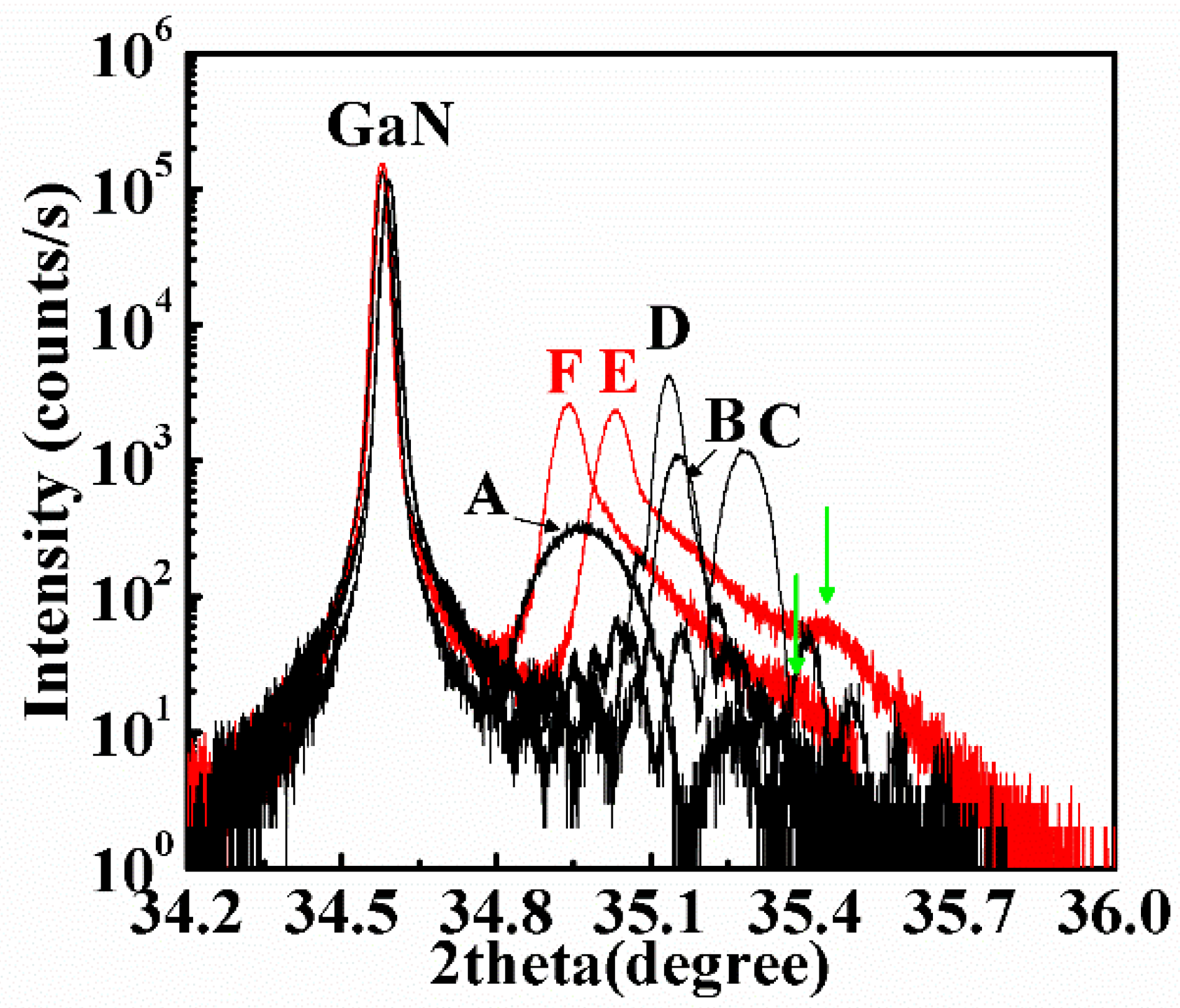
HRXRD (0002) 2θ/ω scanning results of the six typical InAlN samples are shown in Figure 1. Samples A, B, E, and F, InAlN films have been grown on GaN/sapphire substrate, while samples C and D on AlN/sapphire substrate. Clear stripes around the InAlN peak have indicated that the interface between the InAlN and GaN has a good epitaxial quality, from which the thicknesses are determined to be 48 nm for sample A, 136 nm for B, 138 nm for C, and 142 nm for D. The data in Table 1 show their full width at half maximum (FWHM) between 232 and 284 arcsec, which is a good result reported to date. The data in Table 1 also show that the thicknesses of sample E and sample F are 450 nm and 610 nm, respectively. The In content is higher than that of the aforementioned four samples. In samples E and F, two InAlN peaks appear at the right tail of InAlN during 2θ/ω scanning, as shown by the green arrows, revealing the degradation of InAlN crystal quality. Herein, the appearance of the tail peak is caused by the relatively uniform composition of the material and/or the phase separation. Actually, because the length and energy of the bond between AlN and InN are quite different, the AlN and InN are almost insoluble. The growth conditions of AlN and InN materials are two opposites, resulting in a narrow growth window of AlInN and proneness to phase separation. In addition, another possible reason is the existence of a composition gradient in the growth direction of the epitaxial layer, a result of the traction effect, the partial and/or complete relaxation in the epitaxial layer [9]. Through contour fitting, for samples E and F, it is estimated that the inclination angle of the degraded parts is 516 and 543 arcsec, respectively.
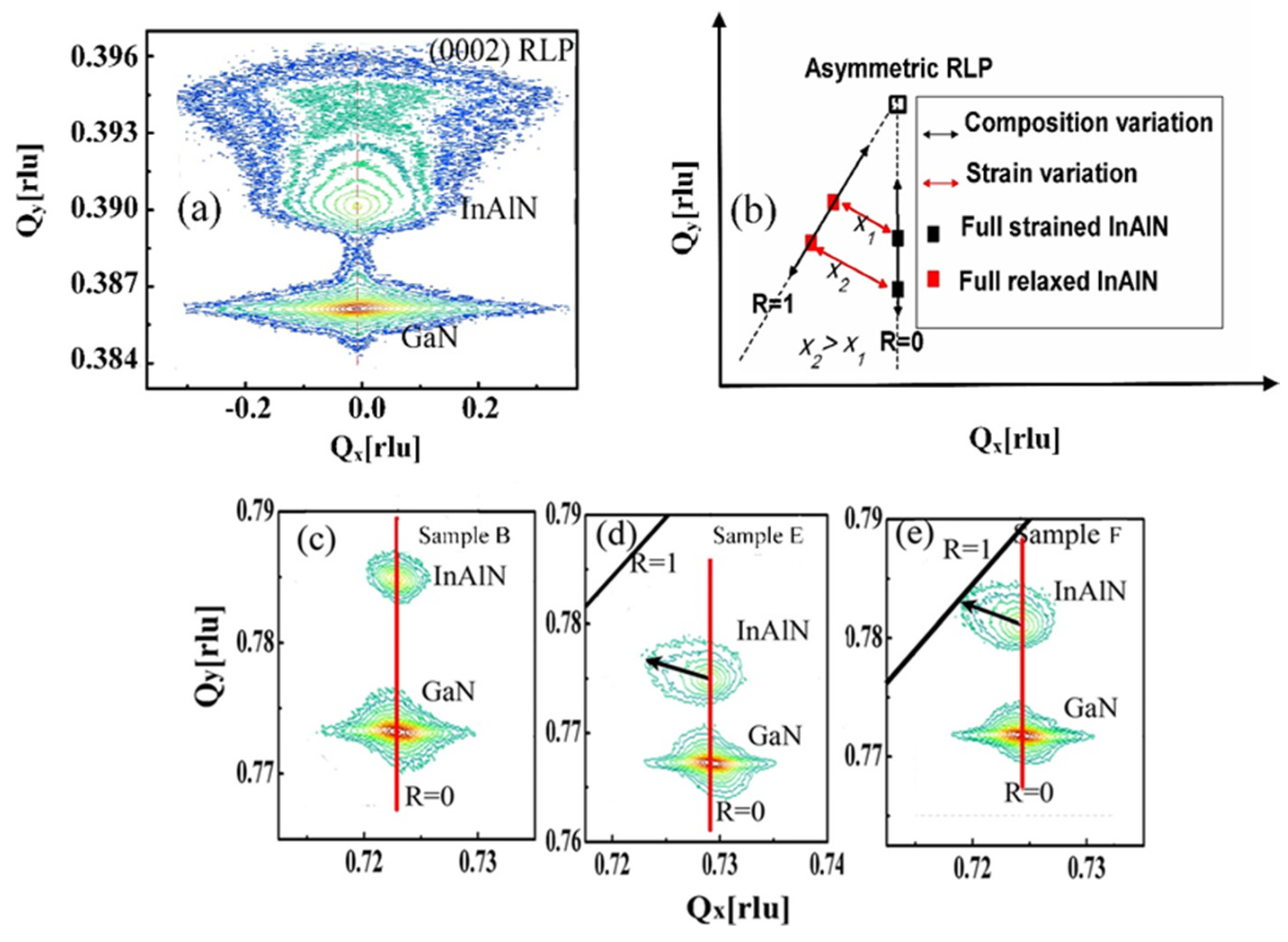
Figure 2 shows the symmetric reciprocal space maps (RSM) around GaN (0002) reciprocal lattice point (RLP) of the sample B, and RSMs around (204) RLP of sample B, E, and F. As shown by the vertical red line (Figure 2a), the transverse position of the diffraction from InxAl1−xN is the same as that from the GaN layer, indicating the pseudomorphic growth of InxAl1−xN with almost none of strain state or the in-plane lattice constants with a full matching between the GaN and InAlN. Figure 2b shows the RSM stress analysis schematic, the marked lines with R = 0 correspond to the full strained InAlN, and the R = 1 marked line corresponds to the full relaxed InAlN. Moreover, basing on the RSM’s results, it can be implied that, with the increase of thickness, the growth of InAlN has changed from the complete coherence of the sample B to GaN, and partial relaxations of the samples E and F as clearly indicated by the black arrows are shown in Figure 2d,e [9]. These above XRD and RSM results have shown that the thick InAlN layers in samples E and F are composed of two sublayers, one of which is coherent to the GaN, and the other one is degraded. It will also be further confirmed by the following characterization of TEM measurement. The InxAl1−xN layers with In composition between x = 0.128 and x = 0.158 exhibit some deviation from the coherent growth in the direction of larger in-plane lattice parameters indicating the compressive strain relaxation [10]. The films with a higher In composition have deviated from the coherent growth in the direction of smaller in-plane lattice parameters revealing the tensile strain relaxation. Therefore, for the specific GaN buffer layer during the epitaxial growth, the lattice matching should occur between x = 0.158 and x = 0.180. However, the lattice matching component (x = 0.180) of the epitaxial layer grown by MOCVD in the InAlN/GaN hetero-structure sometimes shows a component instability [11]. In addition, almost no tilt between the buffer layers and InAlN can be observed in the Figure 2a, which might be directly related to the density of screw-type TDs [12].
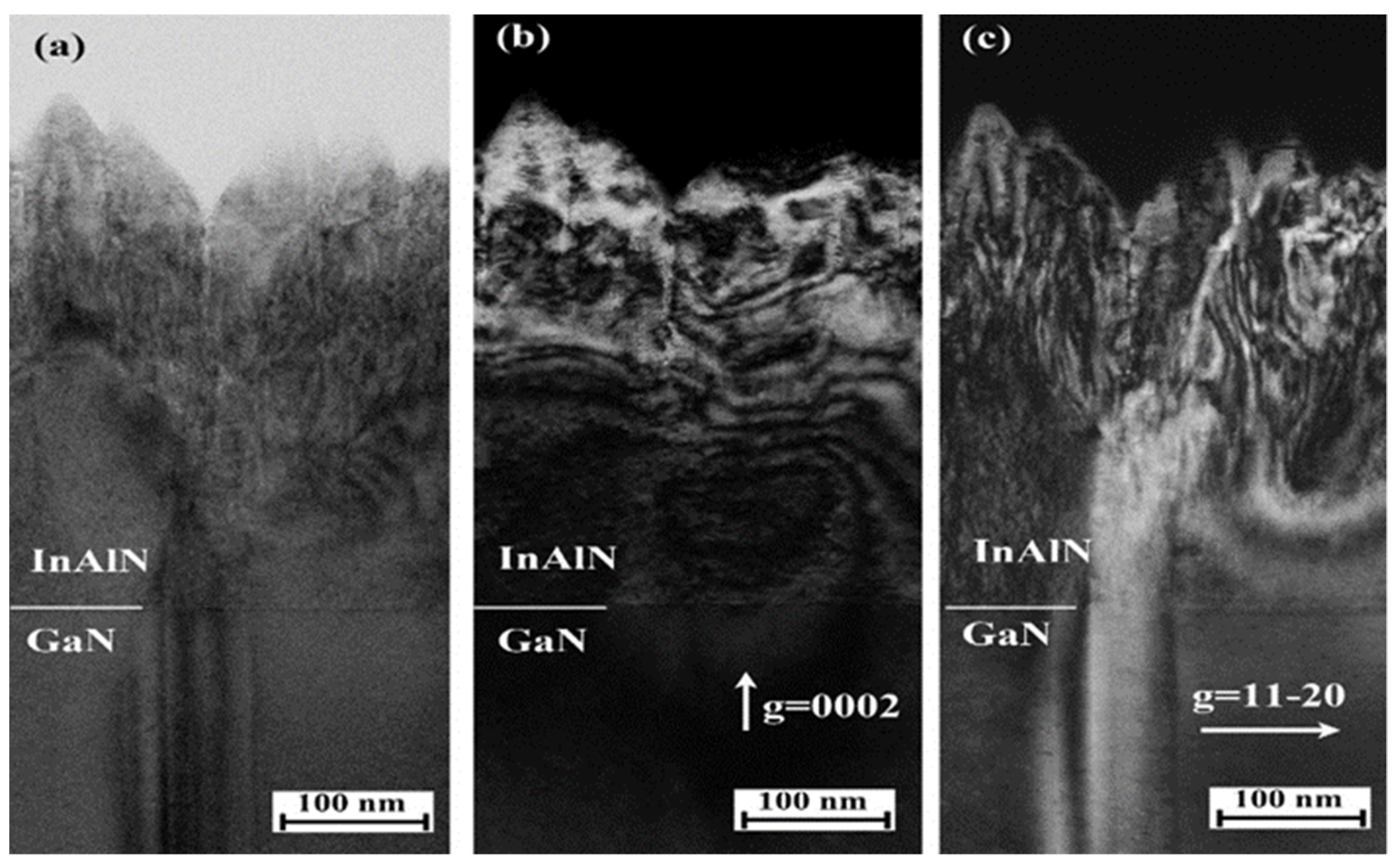
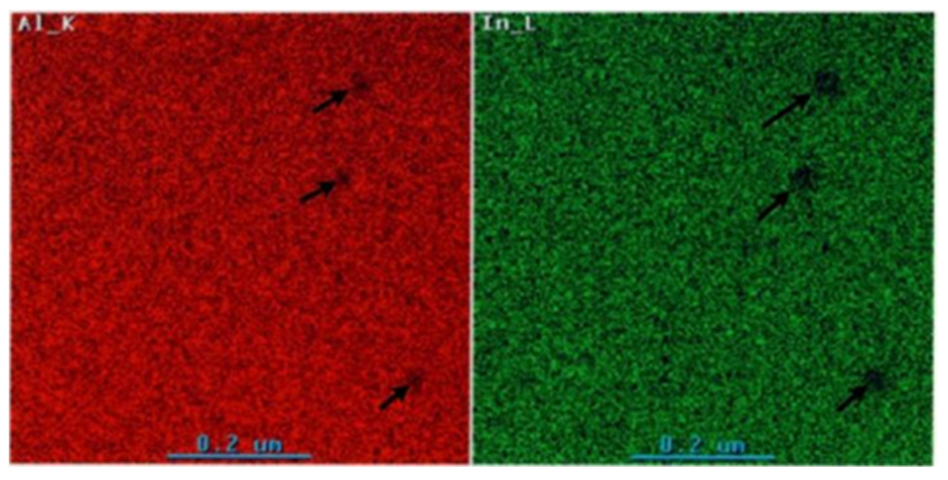
The essential causes of the crystal quality degradation of thick InAlN layer can be evaluated by means of the cross-sectional TEM. Figure 3 shows the micro-structure of 450 nm-thick InAlN sample E. It can be clearly observed that V-type defects have been originating from the TDs in GaN layer, because TDs in the below epitaxial layers have directly altered the nucleation conditions of InAlN, finally resulting in the preferential nucleation near dislocations. Based on a standard diffraction contrast, most of the dislocations are visible, indicating that screw and mixed dislocations are dominant, with Burgers vectors c and c + a, respectively, where a and c are the unit cell vectors in the hexagonal lattice [13]. It is also found in Figure 3a that the defects of InAlN layer have been increasing rapidly as the thickness exceeds 180 nm. The destruction of the composition uniformity has resulted from the propagation of TDs from GaN substrate. These dislocations have begun to transversely bend in an area of the first 100 nm above the InAlN/GaN interface, forming a V-groove with a divergent angle of approximately 36°, which is really approaching the {101} plane. With the strain energy related to the large Burger vector, the TDs continuously expand to form the {101} facets [14,15]. In Figure 3b,c, a significantly thin TEM foil (estimated cross-section thickness of 80 nm) is fused at 200 nm of the InAlN/GaN interface in the fan-shaped region, which derives from the other nearby dislocations, but does not include thin TEM foil and these fan-shaped regions are filled with materials that have a significant decrease in indium content and an expected wide luminescence peak. The stable opening of screw dislocations can be attributed to the local strain generated by random alloy fluctuations. In fact, during the subsequent growth, the crystallites with about 10% indium content form heterogeneous nucleation on the leaned planes of the open-core dislocations. A further explanation is that the 450 nm-thick epitaxial layer is composed of a uniform In0.18Al0.82N layer with a certain thickness, and then the composition decreases linearly to ~ In0.10Al0.90N during the subsequent growth. Consequently, TEM observations have revealed that the structural damages are attributed to the heterogeneous nucleation and growth of it on the V-grooves surface. In addition, the InAlN/GaN hetero-junction interface in the TEM image is clear, however, it can be observed that there is a change in the light and dark contrast, indicating the In segregation phenomenon. From the aforementioned analyses, it can be revealed that GaN/sapphire template with a high crystalline quality has played an important role in the growth of InAlN epilayer. On the other hand, the distribution of indium composition is clear from the EDX maps in Figure 4. In the map of Al and In elements, the InAlN layer has three V-type defects, and has been formed by some dislocation points (shown by black arrows). The outside area of the V-type defects has indicated that when the mass of InAlN has been degraded, no uniform distribution of the In component can be observed in the EDX resolution range, also no phase separations have occurred [16,17]. It is believed that the decrease of indium content is related to the growth on the inclined crystal plane. Specifically, in the growth process of c plane, the drag of components has led to the gas phase rich in Al. The existence of the inclined crystal plane has increased the incorporation of Al and the growth rate. The crystallites have been grown on the V-grooves, which is resemble a columnar structure with a diameter of 15 nm, corresponding to a TD density of 5 × 10¹¹/cm2. The sample’s top surface has reflected the V-groove morphology of the open-core TDs. In fact, these interpretations and descriptions are consistent with the TEM results.
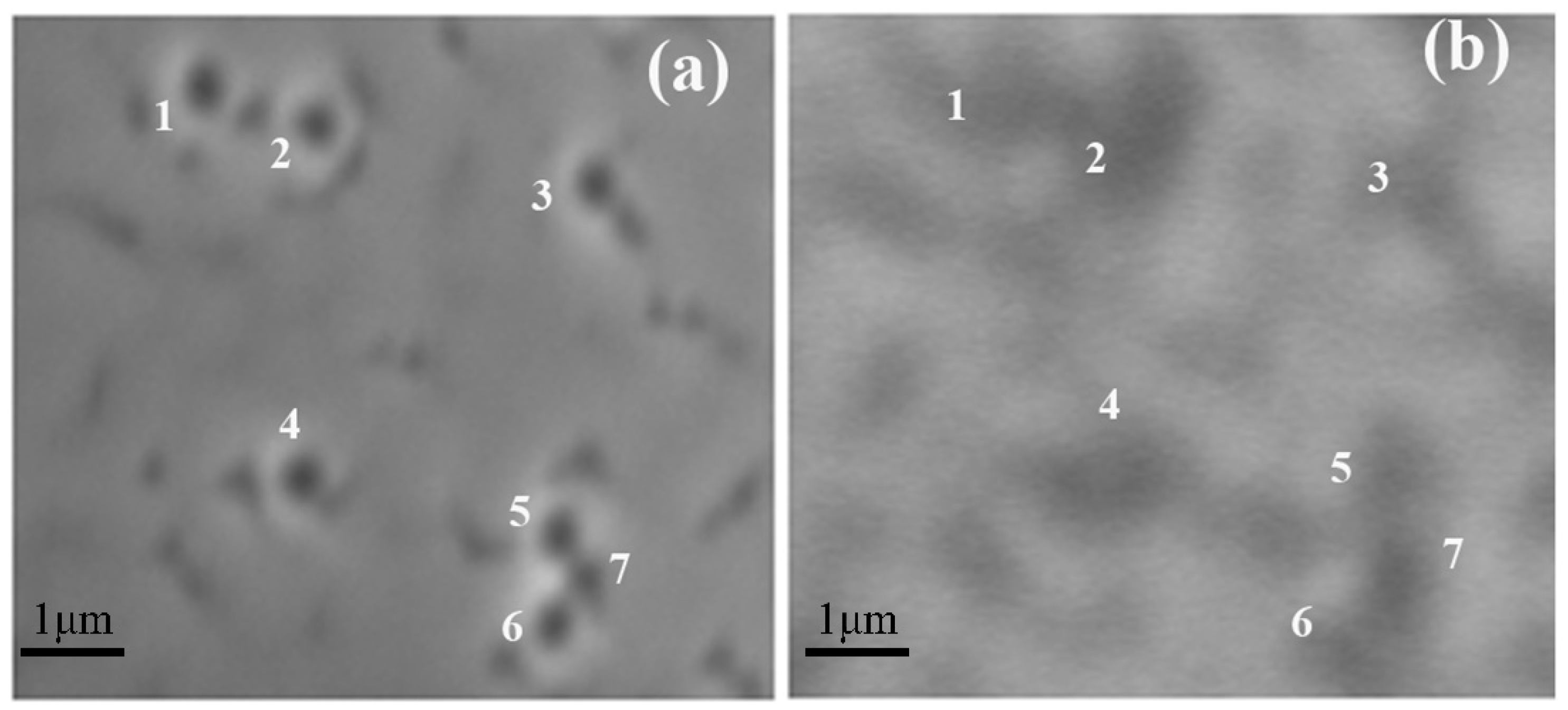
Optical properties of InAlN layer can be evaluated by SEM as shown in the Figure 5. Figure 5a shows the surface morphology of InAlN, whose lattices have matched with the GaN. It can be seen that in the InAlN layer, V-type defects (as shown by the numbers 1 to 7) have formed on the sample’s surface. This is due to that with the growth of InAlN, the distribution of In component is not uniform, more and more In atoms have gathered around TDs by aggregation in a local strained field, resulting in In-rich regions. These In-rich regions always appear as masks when reaching critical sizes [18], which often form V-shaped pits. It should be worth noting that the V-shaped pits have originated from the top of mixed dislocation, it is unrelated to a pure edge dislocation. While in thicker InAlN layers, such as those in sample E and F, these TDs from the underlying GaN layer would have led to the degradation of the crystal quality. The density of the TDs has been estimated to be 2 × 10⁹/cm2. Figure 5b exhibits the monochromatic CL mapping of 136 nm InAlN layer, the excitation energy is 2 KV, and the light detection has been set in the range of InAlN luminescence. It can be found that there are seven dark luminescence regions, while the other regions are bright. Actually, the substrate material would be contributed to the luminescence, depending on the energy released by the electrons from the conduction band to the valence band with generating optical signals. When defects occur in the materials, the defect energy level might be introduced into the energy band. The optical signals are also different, since the energy level gaps are different, which have been relating with the electrons recombination from the defect energy level to the valence band and those from the conduction band to the valence band. As a result, the contrast has appeared, resulting in the defect morphology, which has been shown in Figure 5b, its results have also coincided with the above V-pits TDs in the TEM measurement.
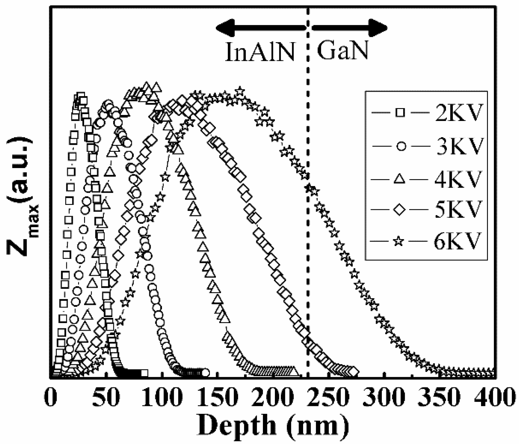
Most of semiconductor devices are composed of layers with different thicknesses in the multilayer structures. As we all know, it is difficult to study the defects of InAlN/GaN hetero-junction by utilizing electron beam (EB), because the penetration depth of the light is limited by the absorption coefficient, and the depths of the deepest layer are often unreachable by the EB. However, these defects can be well imaged by the CL. In addition, the morphology of non-luminous region can be observed by its spectral ability for a better understanding the physical mechanism of degradation. In fact, when the electrons in a form of the EB enter into the sample, they will lose the corresponding energy because of the continuous collision, as a result of which EB has propagated inside the full sample. Figure 6 shows the electron excitation spectra of the InAlN/GaN hetero-junction with the depth in the low EB voltage range based on Monte Carlo simulation [19]. Based on the set of the incident electrons, its simulation of the secondary electron random collisions can more accurately simulate the variation of the electron-hole pairs generation rate with the depth. The higher EB energy it is, the deeper penetration of the electrons would occur in the corresponding sample. As the EB penetrates, the electrons will begin to propagate laterally. The larger the EB energy, the larger the lateral expansion, which often results in reducing the lateral resolution, the same trend as shown in Figure 6. Thus, the highest spatial resolution can be achieved by employing the low-energy EB. However, regarding the multilayer structure, the highest spatial resolution can only lie in the closest layer to the surface, and the deepest layer requires a higher EB energy to excite its luminescence [20].
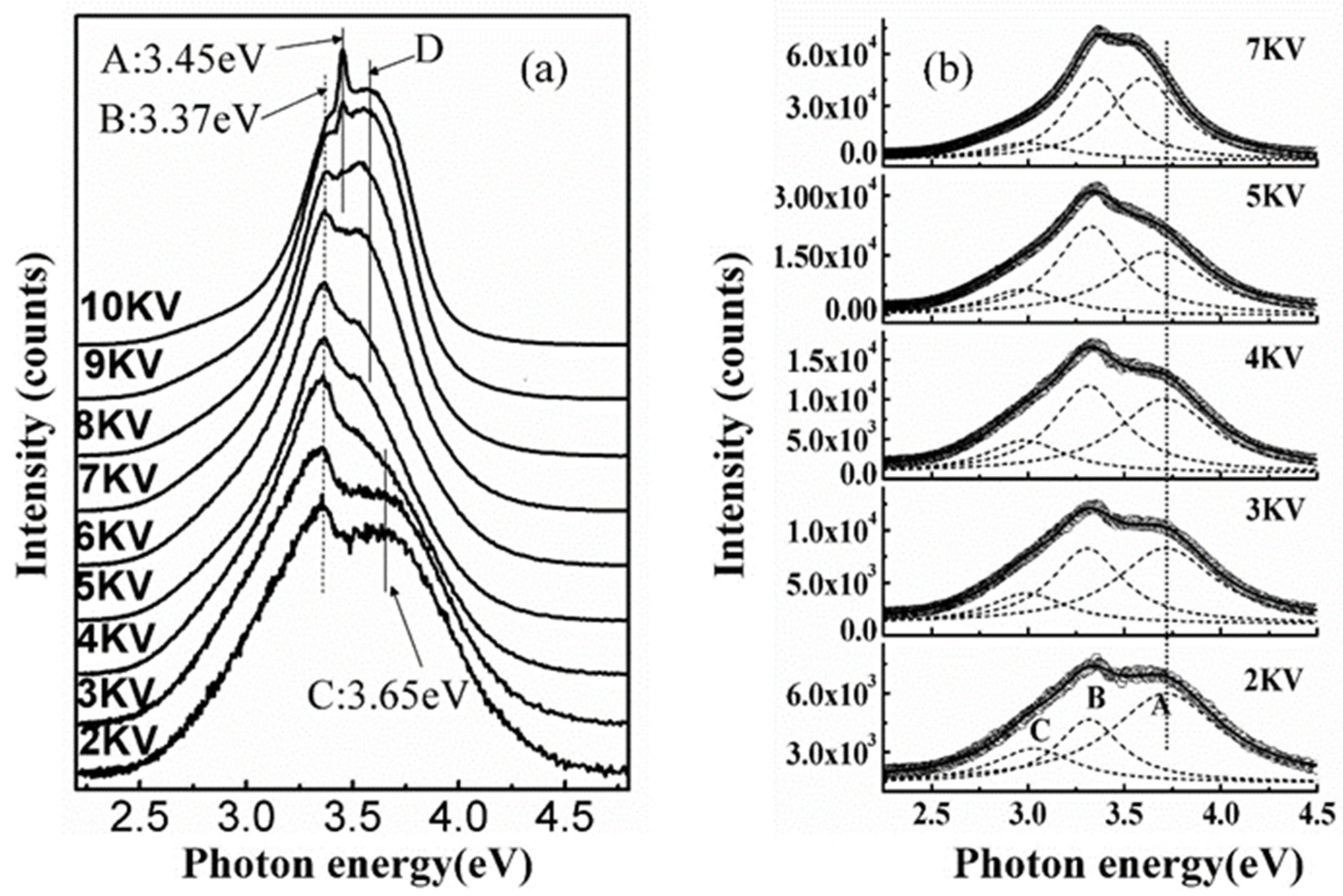
Figure 7 shows the CL spectra under some different acceleration voltages for the 450 nm-thick InAlN sample E. The variation of the InAlN emission peak intensity is an important judgment for its epilayer quality as indicated in the following discussions. CL spectra are corresponding to the acceleration voltage from 2 to 10 KV as shown in Figure 7a. When the acceleration voltage range is between 2 and 8 KV, GaN emission show a characteristic emission peak centered at 3.37 eV (as virtual line B showing). The measurement depth of CL signal can be estimated by Monte Carlo simulation results about 260 nm, therefore its emission peak might have been originating from the GaN dislocations. When the acceleration voltage is further increased to 9 KV and 10 KV, the GaN emission changes to 3.45 eV (shown as line A), which is due to the CL signal reaching the GaN layer, and the emission peak source changes from the TDs in the InAlN layer to the basal-plane stacking fault in the GaN layer [21]. For the InAlN emission, only 3.65 eV of the central emission peak (shown as line C) exists with low acceleration voltage in the range of 2–5 KV. At this time, the CL signal measurement depth is approximate to 100 nm, which is the InAlN crystal quality degradation layer as discussed in TEM. In this layer, due to the serious nonuniform distribution of In components in the V-type defect and more deep energy levels in the InAlN in this region [22], the near-surface CL emission peak has the variation of the peak position and the broadening of spectrum while comparing with the emission peaks at a higher acceleration voltage. It is worth noting that when the acceleration voltage exceeds 5 KV, the resolution of the CL signal increases, and the detected defects in the InAlN layer would be gradually increasing. The low crystal quality in the degradation layer makes it difficult to accurately measure the emission peak energy of InAlN (shown as line D), which often requires much higher precision CL research. In order to explore further reasons for InAlN emission peak shifting, the Gaussian fitting has been carried out to analyze the deconvolution integral peaks of the defect emission in CL spectra (Figure 7b). It can be clearly found that the CL curve is composed of the three fitting peaks (denoted with peaks A, B, and C). With the acceleration voltage range of 2–5 KV, the centered emission peak energy of A, B, C is 3.65 eV, 3.37eV, 3.06 eV, respectively. Peak A has shown a slight red-shifting at an accelerating voltage of 7 KV because the In content in the top InAlN layer is lower than that in the bottom one, resulting in much more InN in the bottom [23]. On the other hand, the sample itself has internal absorption capacity for the CL signal generated by the EB excitation, and the absorption coefficient is related to the EB energy, resulting in the red shift of the emission peak with the increase of the acceleration voltage [24]. Peak B, as the intrinsic peak, has no obvious displacement under the acceleration voltage changes, while peak C has an obvious appearance at some low acceleration voltages, which has resulted from the non-radiative recombination center luminescence in the V-type defects on the surface of InAlN layer [25]. In addition, the emission broadening of peak A in the low accelerating voltage range is due to the degradation of InAlN crystal near the surface. It has also agreed with the previous micro-structural results of XRD, TEM, and EDX characterizations.
4. Conclusions
In summary, the micro-structural properties of InAlN/GaN grown by MOCVD have been systematically characterized through the traditional measurements of HRXRD, TEM, SEM, and CL. Basing on the TEM results, it can be concluded that the thicker InAlN epitaxial layer has exhibited the surface inhomogeneity resulting from the In composition fluctuation. V-type defects have originated from the TDs in the below GaN layer, especially for the beginning area of InAlN layer, and no phase separation can be confirmed in EDX. In addition, the formation of V-type defects and some absence of phase separation has been evaluated and emphasized. Some significant CL spectra with emission peak variations have been further explored and discussed through the Monte Carlo Simulation and Gaussian fitting. Consequently, it can be expected that these characterization results would inspire the researcher to improve the crystalline quality, and even bring about some reasonable structural designs for significant improvements in semiconductor device properties.
Author Contributions
Conceptualization, Y.L. and H.D.; Formal analysis, M.G., M.W. and X.G.; Resources, methodology, data curation, Z.C.; Writing—original draft preparation, T.H.; Writing—review and editing, Y.Z. All authors have read and agreed to the published version of the manuscript.
Funding
This work was supported by the National Natural Science Foundation of China (grant nos. 61874168, 62004109, 62074086, and 62175043) and financial support from the Industry-University-Research Cooperation Project of Jiangsu Province (no. 21ZH626).
Data Availability Statement
Not applicable.
Acknowledgments
The authors would like to gratefully acknowledge the support from the National Natural Science Foundation of China.
Conflicts of Interest
The authors have no conflict to disclose.
References
- Cui, P.; Zeng, Y. Technology of sub-100 nm InAlN/GaN HEMTs on silicon with suppressed leakage current. Solid-State Electron 2021, 185, 108137. [Google Scholar] [CrossRef]
- Alvi, P.A. Enhanced optical gain characteristics of InAlN/δ-GaN/InAlN nanoscale-heterostructure for D-UV applications. Superlattices Microstruct. 2020, 140, 106436. [Google Scholar] [CrossRef]
- Jamil, T.; Usman, M.; Jamal, H.; Khan, S.; Rasheed, S.; Ali, S. High radiative recombination rate of AlGaN-Based deep ultraviolet light-emitting diodes with AlInGaN/AlInN/AlInGaN tunnel electron blocking layer. J. Electron. Mater. 2021, 50, 5612–5617. [Google Scholar] [CrossRef]
- Kuzmik, J. InAlN/(In) GaN high electron mobility transistors: Some aspects of the quantum well heterostructure proposal. Semicond. Sci. Technol. 2002, 17, 540. [Google Scholar] [CrossRef]
- Yakovlev, E.V.; Lobanova, A.V.; Talalaev, R.A.; Watson, I.M.; Lorenz, K.; Alves, E. Mechanisms of AlInN growth by MOVPE: Modeling and experimental study. Phys. Status Solidi C 2008, 5, 1688–1690. [Google Scholar] [CrossRef]
- Kotani, J.; Yamada, A.; Ishiguro, T.; Tomabechi, S.; Nakamura, N. Low dislocation density InAlN/AlN/GaN heterostructures grown on GaN substrates and the effects on gate leakage characteristics. Appl. Phys. Lett. 2016, 108, 152109. [Google Scholar] [CrossRef]
- Bohnen, T.; Yazdi, G.R.; Yakimova, R.; van Dreumel, G.W.G.; Hageman, P.R.; Vlieg, E.; Algra, R.E.; Edgar, J.H. ScAlN nanowires: A cathodoluminescence study. J. Cryst. Growth 2009, 311, 3147–3151. [Google Scholar] [CrossRef]
- Chen, Z.T.; Tan, S.X.; Sakai, Y.; Egawa, T. Improved performance of InAlN-based Schottky solar-blind photodiodes. Appl. Phys. Lett. 2009, 94, 213504. [Google Scholar] [CrossRef]
- Chen, Z.T.; Fujita, K.; Ichikawa, J.; Egawa, T. Threading dislocation-governed degradation in crystal quality of heteroepitaxial materials: The case of InAlN nearly lattice-matched to GaN. J. Appl. Phys. 2012, 111, 053535. [Google Scholar] [CrossRef]
- Darakchieva, V.; Beckers, M.; Xie, M.Y.; Hultman, L.; Monemar, B.; Carlin, J.F.; Gonschorek, M.; Grandjean, N. Effects of strain and composition on the lattice parameters and applicability of Vegard’s rule in Al-rich Al1−xInxN films grown on sapphire. J. Appl. Phys. 2008, 103, 103513. [Google Scholar] [CrossRef]
- Wei, Q.Y.; Li, T.; Huang, Y.; Huang, J.Y.; Chen, Z.T.; Egawa, T.; Ponce, F.A. Compositional instability in InAlN/GaN lattice-matched epitaxy. Appl. Phys. Lett. 2012, 100, 092101. [Google Scholar] [CrossRef]
- Chen, Z.T.; Xu, K.; Guo, L.P.; Yang, Z.J.; Su, Y.Y.; Yang, X.L.; Pan, Y.B.; Shen, B.; Zhang, H.; Zhang, G.Y. Effect of long anneals on the densities of threading dislocations in GaN films grown by metal-organic chemical vapor deposition. J. Cryst. Growth 2006, 294, 156–161. [Google Scholar] [CrossRef]
- Ponce, F.A.; Cherns, D.; Young, W.T.; Steeds, J.W. Characterization of dislocations in GaN by transmission electron diffraction and microscopy techniques. Appl. Phys. Lett. 1996, 69, 770–772. [Google Scholar] [CrossRef]
- Cherns, D.; Young, W.T.; Sanders, M.; Steeds, J.W.; Ponce, F.A.; Nakamura, S. Determination of the atomic structure of inversion domain boundaries in α-GaN by transmission electron microscopy. Philos. Mag. A 1998, 77, 273–286. [Google Scholar] [CrossRef]
- Cherns, D.; Young, W.T.; Steeds, J.W.; Ponce, F.A.; Nakamura, S. Observation of coreless dislocations in α-GaN. J. Cryst. Growth 1997, 178, 201–206. [Google Scholar] [CrossRef]
- Horenburg, P.; Bremers, H.; Imlau, R.; Rossow, U.; Hangleiter, A. Microscopic analysis of interface composition dynamics in m-plane AlInN. Jpn. J. Appl. Phys. 2019, 58, SC1008. [Google Scholar] [CrossRef]
- Rodríguez, R.; Correcher, V.; Gómez-Ros, J.M.; Plaza, J.L.; García-Guinea, J. Cathodoluminescence, SEM and EDX analysis of CaF2 and Tm2O3 pellets for radiation dosimetry applications. Radiat. Phys. Chem. 2021, 188, 109621. [Google Scholar] [CrossRef]
- Watanabe, K.; Yang, J.R.; Huang, S.Y.; Inoke, K.; Hsu, J.T.; Tu, R.C.; Yamazaki, T.; Nakanishi, N.; Shiojiri, M. Formation and structure of inverted hexagonal pyramid defects in multiple quantum wells InGaN/GaN. Appl. Phys. Lett. 2003, 82, 718–720. [Google Scholar] [CrossRef]
- Wong, H.S.; Buenfeld, N.R. Monte Carlo simulation of electron-solid interactions in cement-based materials. Cem. Concr. Res. 2006, 36, 1076–1082. [Google Scholar] [CrossRef] [Green Version]
- Dadgostar, S.; Souto, J.; Jiménez, J. CL as a tool for device characterisation: The case of laser diode degradation. Nano Express 2021, 2, 014001. [Google Scholar] [CrossRef]
- Chen, J.; Yi, W.; Ito, S.; Sekiguchi, T. Cathodoluminescence investigation of stacking faults and dislocations in the edge part of seed grown m-Plane GaN Substrate. Phys. Status Solidi A 2021, 218, 14. [Google Scholar] [CrossRef]
- Chichibu, S.F.; Uedono, A.; Onuma, T.; DenBaars, S.P.; Mishra, U.K.; Speck, J.S.; Nakamura, S. Impact of point defects on the luminescence properties of (Al, Ga) N. Mater. Sci. Forum 2008, 590, 233–248. [Google Scholar] [CrossRef]
- Taylor, E.; Smith, M.D.; Sadler, T.C.; Lorenz, K.; Li, H.N.; Alves, E.; Parbrook, P.J.; Martin, R.W. Structural and optical properties of Ga auto-incorporated InAlN epilayers. J. Cryst. Growth 2014, 408, 97–101. [Google Scholar] [CrossRef] [Green Version]
- Knobloch, K.; Perlin, P.; Krueger, J.; Weber, E.R.; Kisielowski, C. Effect of internal absorption on cathodoluminescence from GaN. Mater. Res. Soc. Internet J. Nitride Semicond. Res. 1998, 3, e4. [Google Scholar] [CrossRef] [Green Version]
- Mohamad, R.; Ruterana, P. Indium segregation mechanism and V-defect formation at the [0001] InAlN surface: An ab-initio investigation. J. Phys. D Appl. Phys. 2020, 54, 015305. [Google Scholar] [CrossRef]
Figure 1.
HRXRD (0002) 2θ/ω scans of the six samples.

Figure 2.
(a) RSM around the GaN (0002) RLP of sample B; (b) RSM stress analysis schematic; (c–e) RSMs around (204) reciprocal lattice point of sample B, E, and F.
Figure 2.
(a) RSM around the GaN (0002) RLP of sample B; (b) RSM stress analysis schematic; (c–e) RSMs around (204) reciprocal lattice point of sample B, E, and F.

Figure 3.
Cross-section TEM dark-field images of the 450 nm-thick InAlN epilayer with (a) bright-field images with g = [110], (b) g = [2], and (c) g = [110].
Figure 3.
Cross-section TEM dark-field images of the 450 nm-thick InAlN epilayer with (a) bright-field images with g = [110], (b) g = [2], and (c) g = [110].

Figure 4.
EDX maps of the sample E with a 450 nm-thick InAlN.

Figure 5.
SEM images of the sample B: (a) Surface morphology of the InAlN; (b) Monochromatic CL mapping of the InAlN.
Figure 5.
SEM images of the sample B: (a) Surface morphology of the InAlN; (b) Monochromatic CL mapping of the InAlN.

Figure 6.
CL Monte Carlo simulation curve.

Figure 7.
CL characterization of the sample E: (a) CL spectra with some different acceleration voltages; (b) Gaussian fitting of the CL spectra.
Figure 7.
CL characterization of the sample E: (a) CL spectra with some different acceleration voltages; (b) Gaussian fitting of the CL spectra.


Table 1.
Some of the structural parameters for the six samples in this study, including the thickness of InAlN (d), the FWHMs of (0002), ω-scanrocking curves, the In contents and template type.
Table 1.
Some of the structural parameters for the six samples in this study, including the thickness of InAlN (d), the FWHMs of (0002), ω-scanrocking curves, the In contents and template type.
| Sample | d (nm) | (0002)FWHM (arc sec) | In Content (%) | Template |
|---|---|---|---|---|
| A | 48 | 256 | 18.1 | GaN/sapphire |
| B | 136 | 232 | 18.4 | GaN/sapphire |
| C | 138 | 263 | 17.5 | AlN/sapphire |
| D | 142 | 284 | 18.7 | AlN/sapphire |
| E | 450 | 258 | 19.0 | GaN/sapphire |
| F | 610 | 275 | 20.7 | GaN/sapphire |
Publisher’s Note: MDPI stays neutral with regard to jurisdictional claims in published maps and institutional affiliations. |
© 2022 by the authors. Licensee MDPI, Basel, Switzerland. This article is an open access article distributed under the terms and conditions of the Creative Commons Attribution (CC BY) license (https://creativecommons.org/licenses/by/4.0/).
Share and Cite
MDPI and ACS Style
Zhu, Y.; Hu, T.; Wang, M.; Li, Y.; Ge, M.; Guo, X.; Deng, H.; Chen, Z. Characterization of the Micro-Structural Properties of InAlN/GaN Epilayer Grown by MOCVD. Crystals 2022, 12, 203. https://0-doi-org.brum.beds.ac.uk/10.3390/cryst12020203
AMA Style
Zhu Y, Hu T, Wang M, Li Y, Ge M, Guo X, Deng H, Chen Z. Characterization of the Micro-Structural Properties of InAlN/GaN Epilayer Grown by MOCVD. Crystals. 2022; 12(2):203. https://0-doi-org.brum.beds.ac.uk/10.3390/cryst12020203
Chicago/Turabian StyleZhu, Youhua, Tao Hu, Meiyu Wang, Yi Li, Mei Ge, Xinglong Guo, Honghai Deng, and Zhitao Chen. 2022. "Characterization of the Micro-Structural Properties of InAlN/GaN Epilayer Grown by MOCVD" Crystals 12, no. 2: 203. https://0-doi-org.brum.beds.ac.uk/10.3390/cryst12020203
Note that from the first issue of 2016, this journal uses article numbers instead of page numbers. See further details here.