1. Introduction
For many decades, solid-state physics research has relied on nuclear measurement techniques, such as perturbed angular correlations (PAC) or Mössbauer spectroscopy (MS), that introduce radioactive isotopes into samples and record their decay, in order to obtain unique information on the local electric and magnetic fields, which in turn reveal a myriad of crucial material properties [
1]. As research moves towards ever smaller and ever more complex nanosystems, these techniques remain a unique source of invaluable information. However, the demands for precision and efficiency of incorporating the right radioactive isotopes becomes more stringent. To meet those challenges, the
apparatus for surface physics and interfaces at CERN (ASPIC) was developed. Since the 1980’s, the ASPIC has performed several experiments in ISOLDE, CERN, which have successfully brought insight into various nanostructures, such as the magnetic hyperfine field at different surface sites of metal films, or magnetic polarization at the interface between ferromagnetic and paramagnetic layers [
2,
3]. However, due to lack of financial support, the experimental setup became unused for more than a decade. Thanks to recent funding by the German agency
Bundesministerium für Bildung und Forschung (BMBF), the ASPIC setup is being refurbished, and upgraded by the incorporation of ultra-low energy (ULE) ion implantation, vastly expanding its ability to extract information on nanostructures in the sub-nanometer range [
4]. To this end, a new chamber is developed that will operate alongside the refurbished ASPIC: the
ASPIC’s ion implantation (ASCII) chamber.
In this article, we present some of the scientific interests that will be pursued using the ASPIC and its new companion chamber, a brief overview of the experimental techniques that will be used in future operation of the chamber, how ultra-low energy ion implantation of radioactive isotopes can enhance these experiments, and finally, we present both chambers and their design.
4. Ultra-Low Energy (ULE) Ion Implantation
In recent decades, ultra-low energy (ULE) or
soft landing ion implantation has enabled the precise modification of surfaces across a wide range of research fields [
16,
17]. The use of ULE energy implantation for 2D materials or thin multiferroic films offers two advantages over conventional ion implantation using energies of several keV. By decelerating ions to energies as low as 10 eV before impinging onto the samples, the implanted ions come to rest in the first (few) monolayer(s), negating the need for additional sample preparation steps, such as post-implantation annealing to activate diffusion of the ions towards the surface. Additionally, a lower amount of energy is deposited in the 2D film, resulting in less defect formation, leaving the structures to be investigated relatively pristine. As such, ULE ion implantation opens up many new ways of studying and modifying surfaces or 2D materials. Indeed, the potential of this technique was recently demonstrated by magnetically doping graphene using Mn ions [
18], or by gaining insight into the behavior of nanometer-sized nanobubbles of noble gas ions [
19].
ULE Ion Implantation of Radioactive Isotopes
Up to now, the application of ULE ion implantation has mostly served as a means of modifying the surfaces and interfaces of nanosystems. However, ULE ion implantation also holds great potential to characterize said surfaces and interfaces by the use of radioactive isotopes as probes. Earlier setups have shown the feasibility of incorporation of radioisotopes at the crystal surface and interfaces [
20], including the ASPIC setup itself (
Section 5) [
2]. A major advantage of this experimental approach is the resolution obtained: as the unstable PAC or Mössbauer isotopes are sensitive only to their local, sub-nm environment (
Section 3), so is the information inferred from recording their decay, rather than laterally or volumetrically averaged as is the case in many other surface science techniques. This does not only allow for atomic depth resolution—a prerequisite for studying 2D materials and their interfaces—, it is crucial for complex crystallographic and magnetic structures with high local anisotropy of electric and magnetic fields, for example in the case of anti-ferromagnetic phases of multiferroics.
Another advantage of using radioactive isotopes is the limited number of ions needed. Since the implanted probes emit radiation themselves—rather than scatter incoming radiation—, the amount of ions needed for sufficient signal collection is low: typically, less than 1 × In/cm are required to perform a PAC measurement with sufficient statistical significance, meaning that even for the atomically thin graphene layer, far less than 1% of atoms is replaced by a foreign species in the most extreme case. Hence, the probes remain dilute in concentration, and do not significantly influence the crystalline structure or composition of the surface or interface.
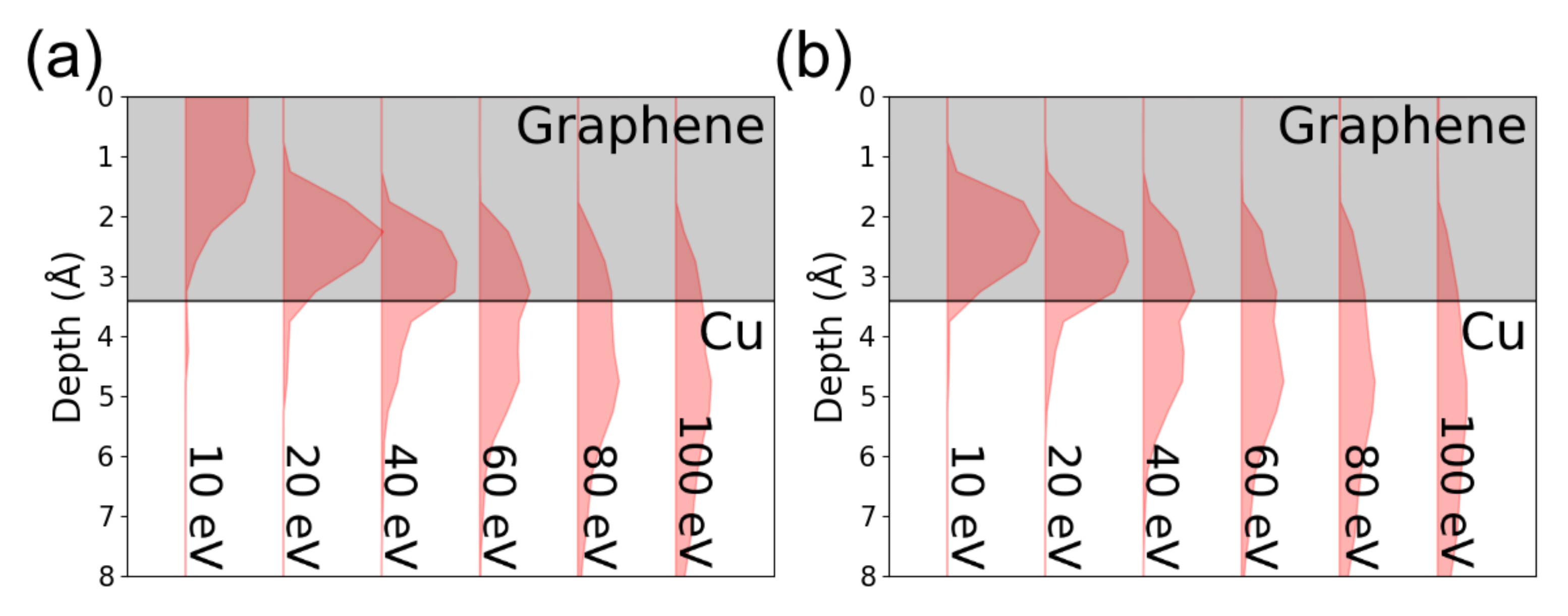
The ability to select the implantation energy freely from 10 to >100 eV in ULE ion implantation setups enables precise control of the depth incorporation of the probes. This can be shown using the IMINTDYN (Ion Matter Interaction -Dynamic) code [
21], an upgraded version of SDTrimSP, itself an upgraded of the SRIM code. This
Monte Carlo simulation code provides detailed cascade information on ions interacting with (amorphous) matter. By modelling a single graphene monolayer on a Cu substrate and varying the implantation energy of the incoming ions, the depth at with different PAC ions (
In and
Pb) come to rest in the system is calculated (
Figure 1). These simulations indeed show that, by tuning the implantation energy accordingly, the radioactive probes can be incorporated at different relevant depths in the nanosystem: the top layer, the interface or deeper into the substrate.
5. Surface Modification and Characterization: Aspic
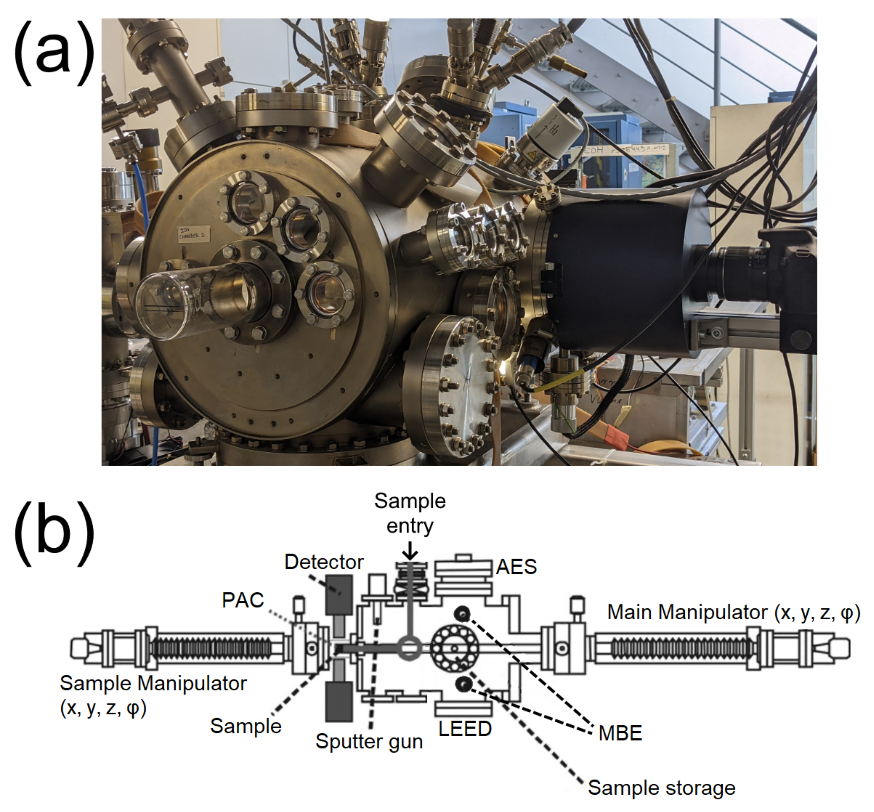
As our scientific interest is focused on atomically thin layers and interfaces, control of the surface and interface state of the sample is crucial. To this end, the ASPIC chamber, shown in
Figure 2, is a powerful tool. In this UHV chamber (≤1 × 10
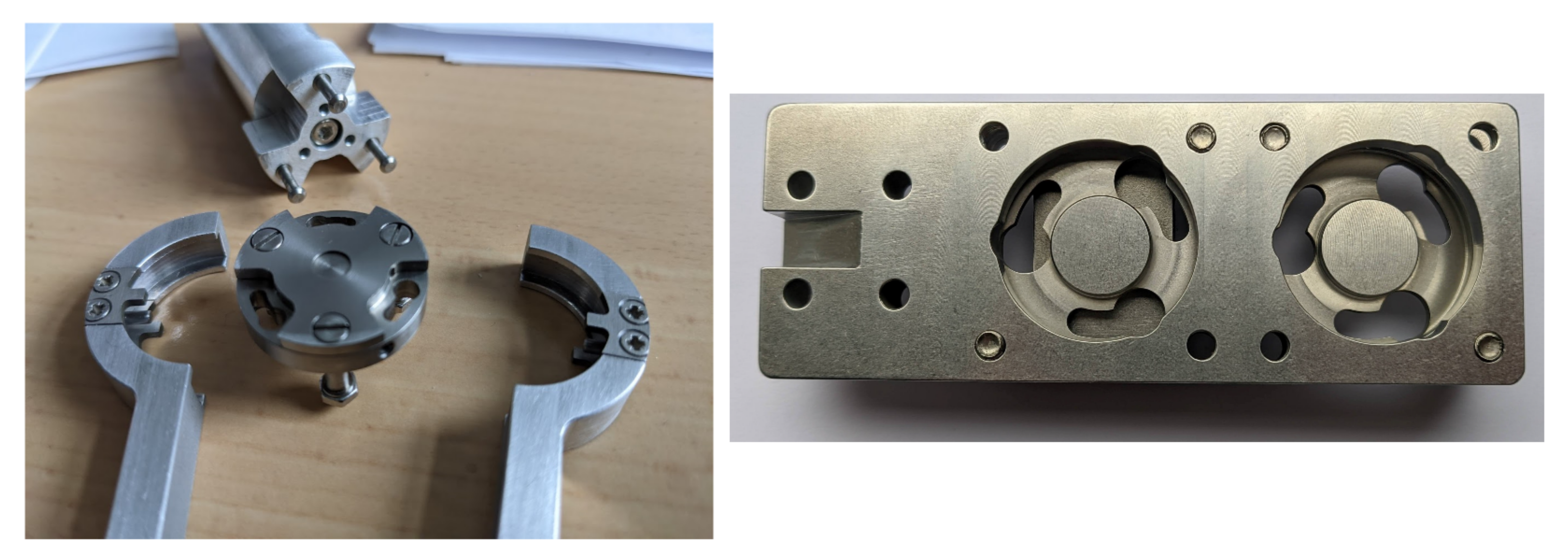
mbar), samples can be prepared and characterized. Before inserting a sample into vacuum, it is mounted into a small sample holder, which in turn can be locked into the custom-made manipulator, using a bayonet system keeping it in place (
Figure 3). This main manipulator arm can rotate around its axis, and can transport the sample to different positions in the chamber along its long dimension. By fully extending the manipulator, the sample is positioned in a half-closed glass tube, around which PAC or Mössbauer detectors can be placed. This allows for the sample to be prepared, characterized (see below) and the radioactive decay of the implanted radioisotopes to be recorded in situ, without breaking the vacuum. This would be crucial for systems sensitive to air exposure, or for experiments involving short-lived isotopes that need to be measured immediately upon implantation. A second, optional sample manipulator arm can also be installed, dedicated to in situ experiments, freeing up the main manipulator for a second sample, whose surface can be already be prepared during the recording of the first sample, using the surface modification and characterization techniques described below, making more efficient use of limited beam time. These manipulators provide a broad temperature range at which experiments can be conducted, as they can be heated to high temperatures (>600
C) or cooled down to cryogenic temperatures using liquid nitrogen: they are equipped with a ceramic heater, a reservoir for liquid nitrogen and the appropriate thermocouple sensors (type K and T) for precise control of the sample temperature.
The other capacities of the ASPIC chamber are divided into two categories: surface modification and surface characterization techniques. The surface modification capabilities of the ASPIC chamber include the following: An ion sputter gun is available to remove impurities and surface layers of samples, using accelerated Ar
ions impinging on the sample at a large angle to the surface normal (60–80
), to increase sputter yield. Often, this sputtering amorphizes the otherwise crystalline surface of the sample. To overcome this, the sample holder can be heated to high temperature, allowing most crystal surfaces to recrystallize. Two molecular beam epitaxy (MBE) evaporators are installed in the chamber, enabling thin films to be deposited onto the sample surface. The choice of material can be adjusted to specific experimental needs, by installing a rod of the appropriate material in the MBE crucible prior to the chamber evacuation. This material could be transition metals of interest, such as ferromagnetic elements like Ni and Fe, or carbon rods, which would aid the preparation or repair of graphene layers. As mentioned above, the sample holder can be heated during deposition, facilitating the deposition of epitaxial layers or surface reconstruction. The deposition of new films is crucial for the study of interfaces: after implanting radioactive probes at or very near the surface of the sample substrate (
Section 4), a thin film can be deposited on said surface, resulting in probe atoms residing now at the interface [
2].
The surface characterization techniques in the ASPIC chamber consists of Auger electron spectroscopy (AES) and low-energy electron diffraction (LEED). Both techniques impinge an electron beam perpendicularly onto the sample surface, and measure the electrons emerging. In the case of LEED, the low-energy electrons (0–800 eV) are diffracted by a crystalline surface, and the diffracted electron form a diffraction pattern of a fluorescent screen. This way, the crystallinity (or lack thereof) of the sample surface can be monitored and recorded, using a camera mounted onto the chamber. In the case of AES spectroscopy, the higher energy electron beam (3–5 keV) knock out inner-shell electrons of the sample atoms, leaving a vacancy that is quickly filled by an electron from a higher-lying shell. The energy released during this vacancy filling is transferred to an “Auger-electron”, emerging from the sample surface with a characteristic kinetic energy. By recording these electrons, a compositional fingerprint of the surface is obtained. The information provided by these two techniques allows experimenters to assess the general state of a sample’s surface, including such information as to whether the sputtering of the surface has removed all contaminants, whether the deposited films cover the entire surface, or whether the sample surfaces have recrystallized due to the sample heating. Finally, the measuring axes of the two devices lie in the same plane perpendicular to the sample holder axis of transportation, as do the MBE evaporators (see
Figure 2b). This does not only allow fast characterization, but enables use of the electron beam for real-time monitoring during film growth. By impinging the AES electron beam onto a sample that the MBE evaporators are depositing upon at a small grazing angle, the reflected particles hit the fluorescent LEED screen, and the growth of the film can be monitored by means of medium-energy electron diffraction (MEED).
In the earlier decades of the ASPIC setup, a custom “catcher” system was used to incorporate the radioactive ions at the surface on the sample. This catcher system consisted of a foil onto which the high-energy ion beam (≤60 keV) was impinged. By heating this foil to high temperature, the ions diffused to the surface, and were subsequently evaporated onto another transfer foil, or directly deposited onto the sample surface. In this way, the ions are deposited onto the sample surface with thermal energy (i.e., E ≤ 10 eV). Although this method successfully incorporated PAC isotopes at the surface or interface [
2,
3], it had a number of drawbacks, most noticeably the inability to carefully control the energy of the deposited ions. Indeed, to place the probes at an interface, this system relied on the post-implantation growth of films in the ASPIC chamber. Not only does this step cost valuable time—decreasing the probe signal and lowering the overall sample throughput during beamtimes—, not every nanostructure is easily grown using MBE evaporators, e.g. a Mn-doped graphene layer [
18]. ULE ion implantation offers a faster, more reproducible and more tunable incorporation of radioactive isotopes (
Section 4). To upgrade the experimental capabilities of the ASPIC to include ULE ion implantation, a brand-new chamber is introduced: the ASPIC’s ion implantation (ASCII) chamber.
6. ASPIC’s Ion Implantation Chamber: ASCII
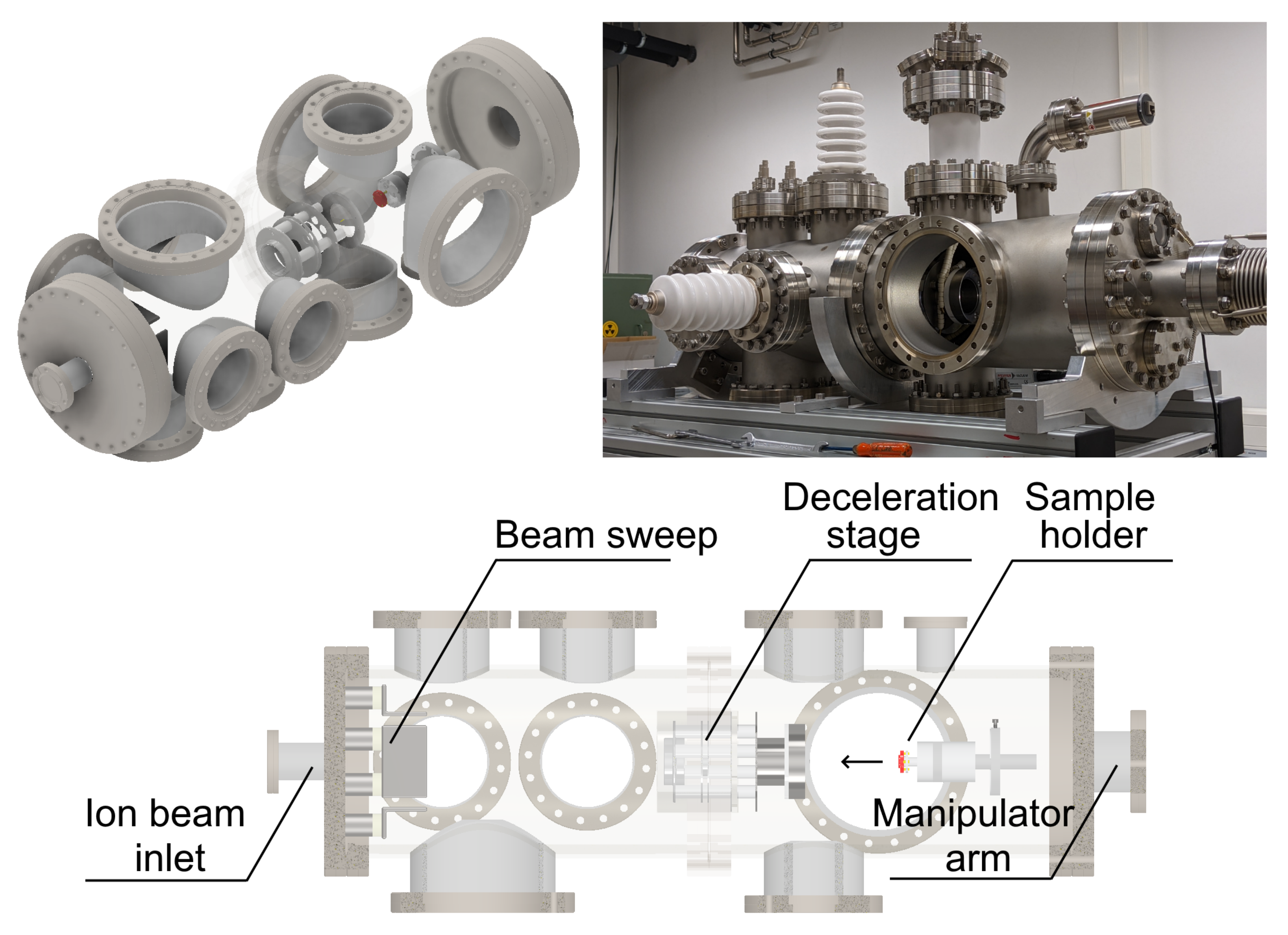
The new ASCII vacuum chamber is shown in
Figure 4. Just like the ASPIC chamber, it is kept at ultra-high vacuum, i.e., ≤
mbar. The three main components of the chamber are the deflector plates near the ion beam inlet, the deceleration stage and the sample manipulator. The deflector plates, each with its own bipolar power supply of ≤3 kV, are used to steer the ion beam onto the entry of the deceleration stage, and/or to sweep it over a small angle (at most 1.5
). The sweeping pattern used is a Fermat’s spiral [
22], assuring the ions are distributed uniformly over the entire solid angle, allowing a conform coverage of the desired irradiated area (see below).
The sample manipulator is equipped with a bayonet system, similar to the one found in the ASPIC chamber, that can lock and hold the small sample holder. Its arm can be moved backwards, to exchange the sample, or forward into the deceleration stage, to position it for ion implantation. Additionally, the manipulator contains a heating element and a K-type thermocouple sensor, allowing implantation to be done at precisely controlled elevated temperature (≤300 C). This readily reduces the implantation-induced defects, or increases the diffusion of the probe atoms into substitutional positions in the crystal.
The design of the deceleration stage draws inspiration from another ULE ion implantation device that has proven itself as a valuable tool for the modification of 2D materials [
18,
19]: the ADONIS (
Anlage zur Deposition niederenergetischer Ionen auf Substrate) setup of the Georg-August-University Göttingen [
23]. The ADONIS setup accelerates (stable) ions using a voltage of 30 KV, and directs them onto the sample, which is held at the same voltage that was used to accelerate the ions initially, minus a small bias voltage (typically 10–100 V). As a result, the ions come to rest with an energy proportional to the tunable bias voltage, e.g. a bias voltage of 20 V results in singly-charged ions impinging with an energy of 20 eV. The ASCII operates on the same principle: by precisely tuning the voltage at which the sample is held, the radioactive ions provided by ISOLDE can be implanted at ultra-low energies. As the sample voltage is freely chosen, any ion energy between 0 eV and 60 keV is technically possible, a capability that could be exploited to study nanostructures at different depths over several nm. In what follows however, we will focus on ULE ion implantation (≤100 eV).
A cross-section of the deceleration stage is shown in
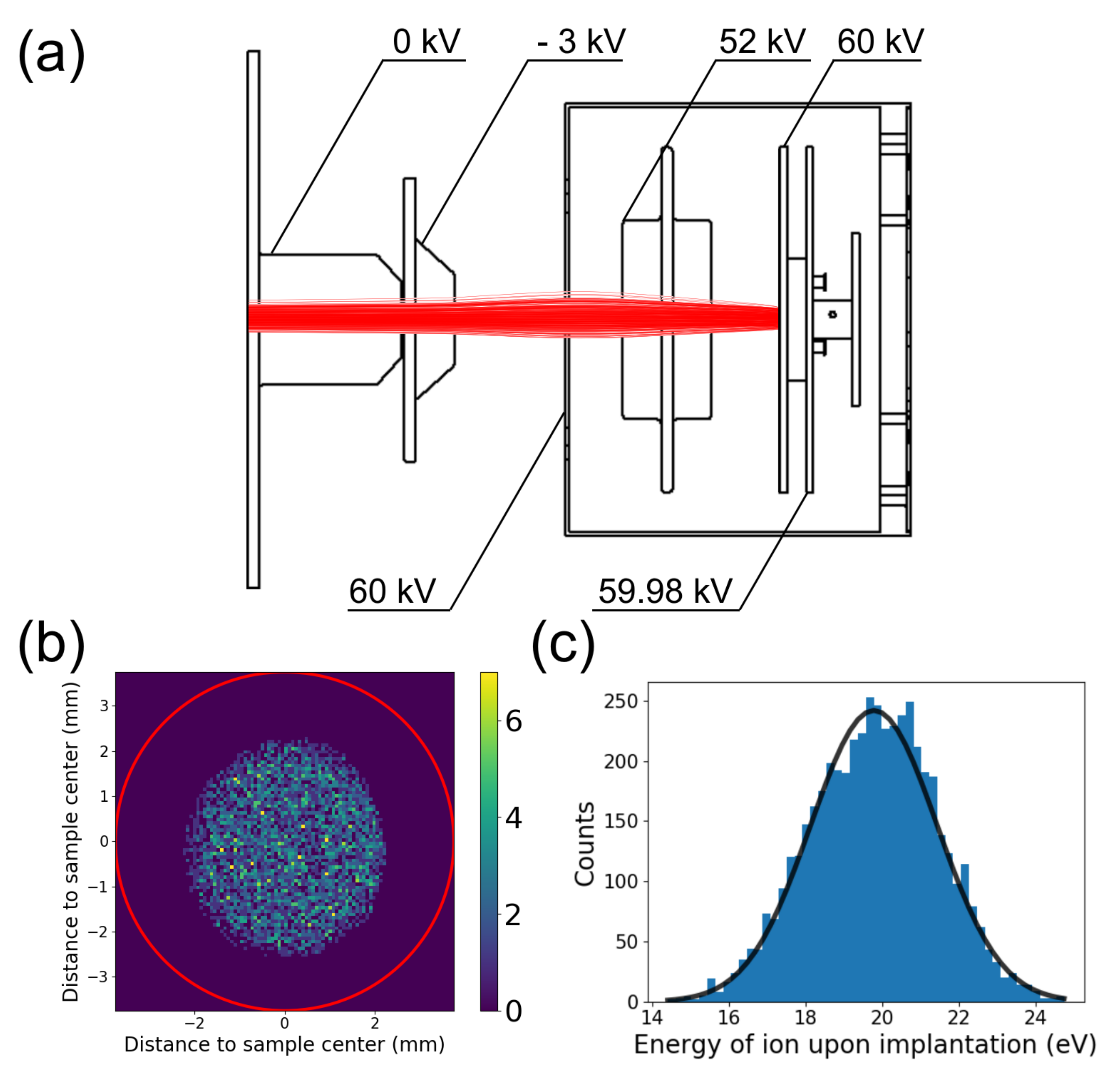
Figure 5, alongside some exemplary voltages that one might use during implantation, as informed by ion beam optics simulations (see below). Its three main components are (left to right) the
electron lens, the
focusing lens and the
sample plates. The electron lens, kept at negative voltages, serves as a way of removing the unwanted electrons—generated by ions colliding with the rest gas—from the positively charged ion beam. Without this step, the amount of implanted ion, deduced from the implanted charge measured at the sample holder, would be significantly underestimated. The focusing lens, kept at 52 kV in this example, determines the area that is irradiated by bending the ions toward the center of the deceleration stage. Finally, the sample plates, one of which is connected to the sample holder and held at the ion acceleration voltage minus the desired bias voltage i.e., 60 kV − 0.02 kV = 59.98 kV, determine the energy with which the ions are implanted into the sample.
Modelling the deceleration stage in the SIMION simulation code [
24], one can investigate the behavior of the ion beam, and optimize the electrostatic voltages of the components to achieve the desired implantation of ions. Such simulations provide complementary insight to the experimental tests of the physical setup, which are currently ongoing. Amongst the most important parameters are the energy distribution of the implanted ions and the percentage of ions that do not hit the sample and are lost; both parameters are ideally as low as possible. By varying the voltages of the different electrostatic components and simulating the ion beam, one can find suitable voltage configurations. The simulation results of one such voltage configuration is shown in
Figure 5. In these simulations, a 60 keV
In beam enters the chamber, is swept over a small angle (≤1.5
), (de)focused and decelerated by the deceleration stage. This beam is modeled on realistic estimates of the ion beams available at ISOLDE: although the beam profile and current differ from ion to ion, typical values are a diameter of around 2 mm, and a current of around 50 pA. In this simulation, a total of 5000 particles were released at the ion beam inlet towards the sample holder, at various times to include the effects of the beam sweep. Whether, where and with what energy these ions impinge onto the sample is recorded. The simulations indicate that all ions reach the sample holder, are uniformly distributed over a ∼6 mm
irradiated area of the sample, and—assuming a Gaussian energy distribution of 2 eV upon entry into the chamber, which the ISOLDE facility can provide—have an energy of 19.8 ± 3.3 eV upon implantation. These simulations show the feasibility of implanting PAC or Mössbauer probes in an efficient way, allowing the experimenter to select both the irradiated area and the implantation energy of the ions, enabling precise control over the depth of the radioactive probes (
Section 4).
7. The Combination of the ASPIC and ASCII Chambers in the Isolde Experimental Hall: Present and Future
Above, the capabilities of the ASPIC and ASCII chambers were discussed separately. However, their strengths will be combined by connecting the two chambers, allowing samples to move quickly from one chamber to the next in a shared ultra-high vacuum. The connecting vacuum tube, in which samples are transported from one chamber to the next using a conveyor belt system, is currently being designed. Such a connection would enable short-lived isotopes to be implanted in the ASCII chamber, quickly transferred to the ASPIC sample manipulator, and measured in situ without ever breaking vacuum. Operating both chambers in this way would enable higher sample throughput, higher amounts of decays recorded, and open up possibilities of using shorter-lived isotopes than those typically used during experiment campaigns (elements with a half-life of 40 min–1.5 h).
The exact installation location of the two chambers in the current ISOLDE experimental hall has not yet been decided. In the 1990’s, the ASPIC chamber was originally connected to the VITO beam line [
25], a setup now dedicated to nuclear and biophysics. However, due to other, newly installed components at this beam line, the ASPIC can no longer be installed there. At the time of writing, the final tests of the chambers’ functionality are being performed, and their installation at the ISOLDE is expected for the end of 2022, beginning of 2023.


