Article

Fully Relaxed, Crack-Free AlGaN with upto 50% Al Composition Grown on Porous GaN Pseudo-Substrate

1
Department of Electrical and Computer Engineering, University of California, Santa Barbara, CA 93106, USA
2
Department of Electrical and Computer Engineering, University of Wisconsin-Madison, Madison, WI 53706, USA
*
Author to whom correspondence should be addressed.
Crystals 2022, 12(7), 989; https://doi.org/10.3390/cryst12070989
Submission received: 20 June 2022 / Revised: 11 July 2022 / Accepted: 12 July 2022 / Published: 16 July 2022

Abstract

:
Fully relaxed, crack free, smooth AlxGa1−xN layers with up to 50% Al composition were demonstrated on pseudo-substrates composed of dense arrays of 10 × 10 µm2 compliant porous GaN-on-porous-GaN tiles. The AlGaN layers were grown in steps for a total of 1.3 µm. The growth conditions necessary to demonstrate high quality films at higher Al compositions also suppressed any sidewall growth.
Keywords:
AlGaN; Porous GaN

1. Introduction

The wide bandgap tunability range of (Al,Ga)N from 3.4 eV for GaN to 6.1 eV for AlN allows for its use in deep ultraviolet (UV) light emitting diodes (LEDs) in fields such as medical disinfection, water purification, biochemical detection and UV curing [1,2,3,4,5,6]. In addition, high power UV laser diodes (LDs) are needed for solar-blind non-line-of-sight communications, UV spectroscopy, laser lithography, and optical data storage [7,8,9,10,11]. Recently, photonics integrated circuits have been of interest for developing self-powered UV photonics systems that can work sustainably and independently with a reduced size and power consumption for future on-chip optical communication [12,13,14,15,16,17,18]. For all these applications, high quality, large area AlGaN substrates are needed. Bulk AlN substrates with a low dislocation density are the ideal candidate [19,20,21,22,23,24]; however, they are currently very expensive and only available in small sizes [25,26]. When AlGaN is grown on foreign substrates such as silicon, sapphire, and silicon carbide, the lattice mismatch usually leads to films with a relatively high density of threading dislocations [27,28]. This is the main cause for non-radiative recombination, leading to the deterioration of the optical and electrical performance of AlGaN UV optoelectronic devices [1,4,27]. When grown hetero-epitaxially on GaN, the lower lattice constant of AlGaN leads to tensile strain and cracking with epilayers thicker than the critical thickness [29,30]. Using lateral overgrowth of buried cracks, relaxed Al0.2Ga0.8N layers on GaN templates were formed using plastic relaxation [31]. Lateral growth of AlGaN on porous GaN or AlN base layers has also been pursued in an effort to reduce the dislocation density [32,33]. Several research groups have also attempted to use a sacrificial layer for flip chip UV LEDs [34].
Recently, 10 × 10 µm2 patterned compliant porous GaN pseudo-substrates (PSs) were formed [35]. Due to its high surface-to-volume ratio, porous GaN exhibits reduced mechanical stiffness with increased porosity [36], similar to porous silicon [37], facilitating the elastic relaxation of InGaN grown on porous GaN PSs [38,39]. On these patterned compliant pseudo-substrates, the growth of 1.3 µm thick crack free, elastically relaxed AlGaN with a low Al composition was also demonstrated [40]. In this work, we performed the deposition of fully relaxed AlGaN with an Al composition of up to 50% on similar GaN-on-porous-GaN PSs.

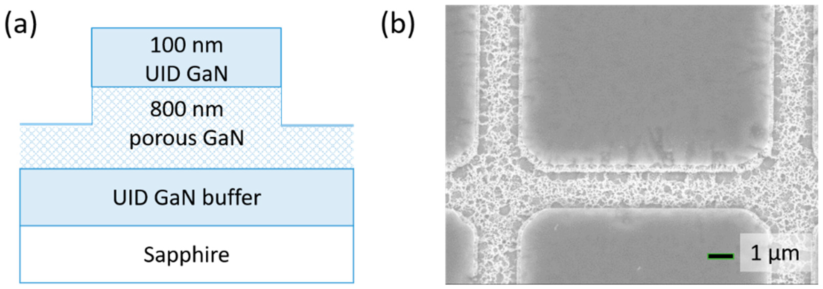
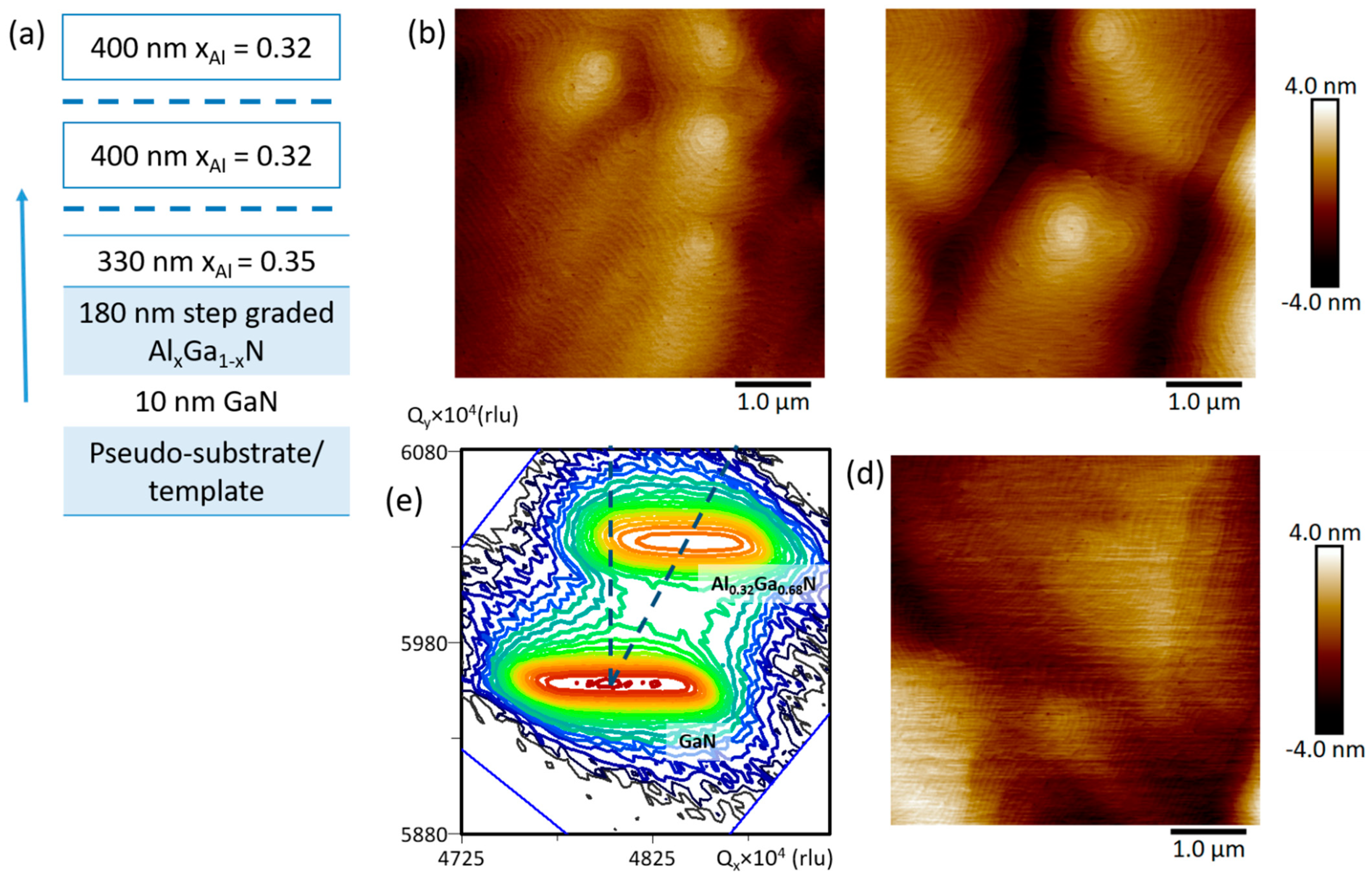
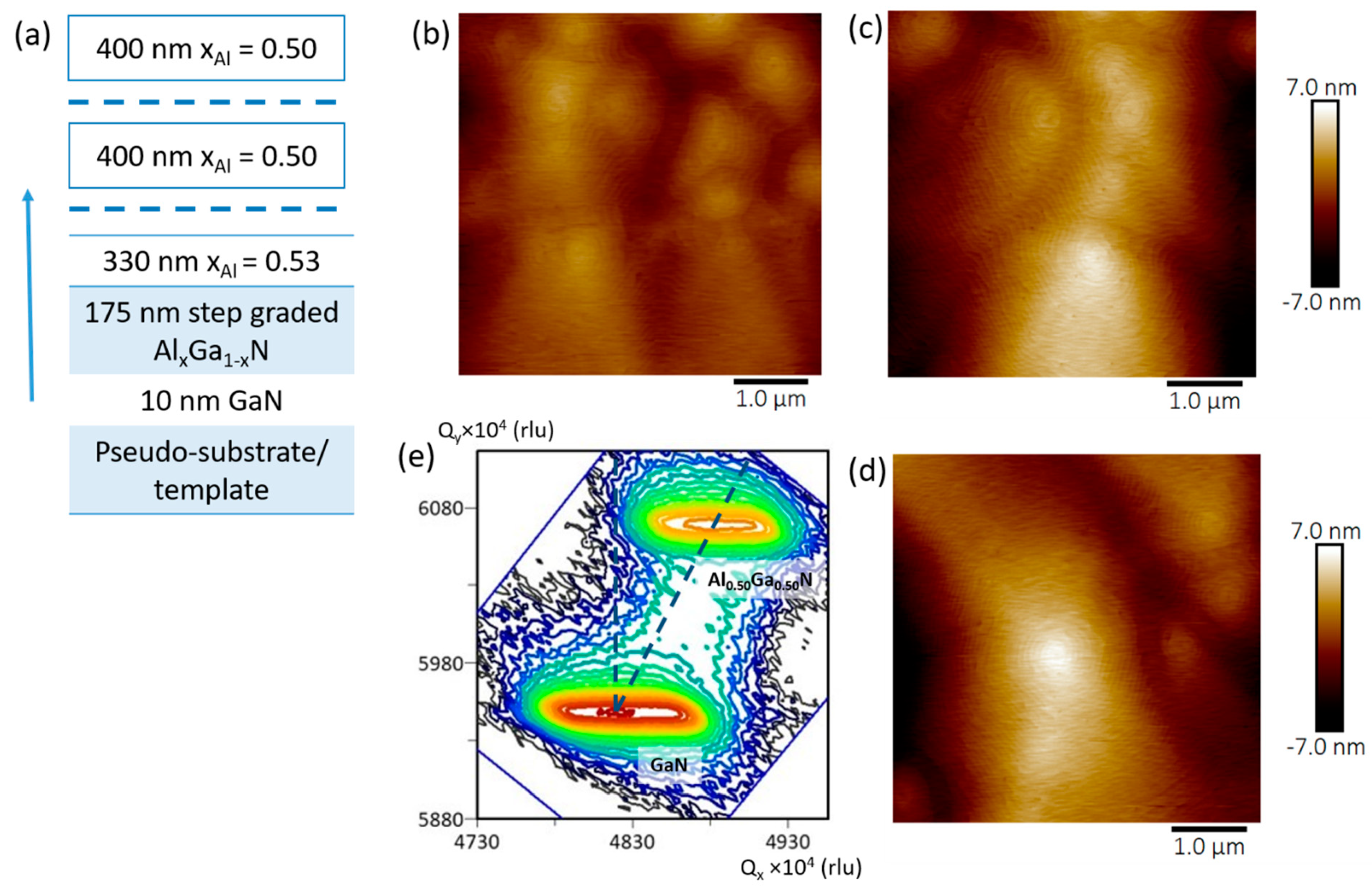
2. Materials and Methods

The layer structure used for porosification as the pseudo-substrate consisted of a 2.8 µm thick unintentionally doped (UID) GaN on c-plane sapphire followed by 800 nm Si doped GaN with a doping of 5 × 1018 cm−3 which was capped with 100 nm of UID GaN. The sample was patterned and dry etched with a 100 W BCl3/Cl2 etch, forming 10 × 10 µm2 square tiles 2 µm apart and with an etch depth of 600 nm. The sidewalls of the tiles were aligned parallel to the orthogonal GaN [1 1 ¯ 00] and GaN [11 2 ¯ 0] planes, respectively. The GaN:Si layers were then porosified with a doping selective electrochemical (EC) etch in 0.3 M oxalic acid with metal contact to the sample with anode and Pt wire acting as the cathode [41]. The current flowing through the sample caused a redox reaction resulting in GaN:Si etching, which formed GaN tiles with embedded porous GaN as depicted in the schematic in Figure 1a and as reported previously [35].
The epitaxial layers in this study were grown by metal organic vapor phase epitaxy (MOVPE) in a close coupled showerhead reactor using the precursors trimethylgallium (TMGa), trimethylaluminum (TMAl), and ammonia (NH3) on the c-plane porous GaN pseudo-substrates at a pressure of 100 Torr. In our previous work, a total of 1.3 µm thick elastically relaxed AlGaN with xAl = 0.18 was demonstrated using a growth temperature of 1080 °C and a mixture of hydrogen and nitrogen as the carrier gas [40]. To obtain good quality AlGaN films with a higher Al composition, the deposition temperature was increased to 1155 °C [42,43], and the NH3 flow was decreased to 45 mmol/min from 178 mmol/min [40]. The molar flow of TMGa varied at 8.8–14.6 µmol/min and TMAl was in the range of 0.98–2.4 µmol/min, respectively. However, growth under these conditions on the GaN-on-porous-GaN PSs resulted in the formation of circular islands on the sample surface (Figure 2a). While the higher growth temperature of 1155 °C was necessary to achieve high quality AlGaN at the targeted composition, it was not suitable for deposition on the GaN-on-porous-GaN PSs. In order to achieve smooth layers, a two-step process was implemented, where the initial 120–130 nm of AlGaN was grown at 1080 °C in a nitrogen ambient atmosphere, after which the temperature was increased to 1155 °C for the rest of the run and the subsequent AlGaN growth was performed in a hydrogen ambient atmosphere.
The 1.3 µm thick AlGaN layers were grown in steps, and before every regrowth the sample was solvent cleaned with acetone and isopropanol which was followed by a buffered HF dip and rinsing with deionized water to remove contaminants and the oxide layer introduced during characterization. The surface morphology was characterized using an optical microscope and atomic force microscope (AFM). High resolution x-ray diffraction (XRD) was used for rocking curve measurements to evaluate the film quality. Reciprocal space maps (RSMs) were taken using XRD around the GaN ( 1 ¯ 1 ¯ 24) reflection. Composition and relaxation were determined from these RSMs using X-Pert Epitaxy software [44,45].

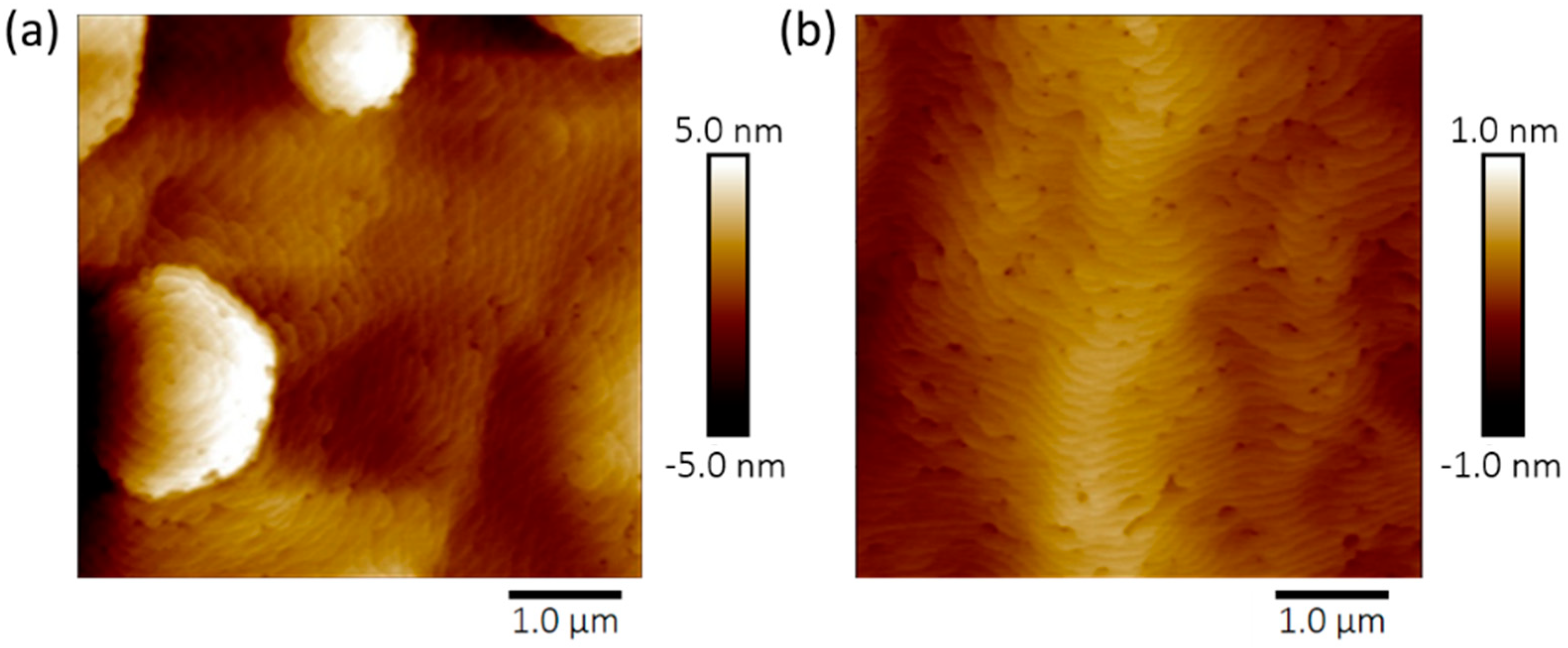
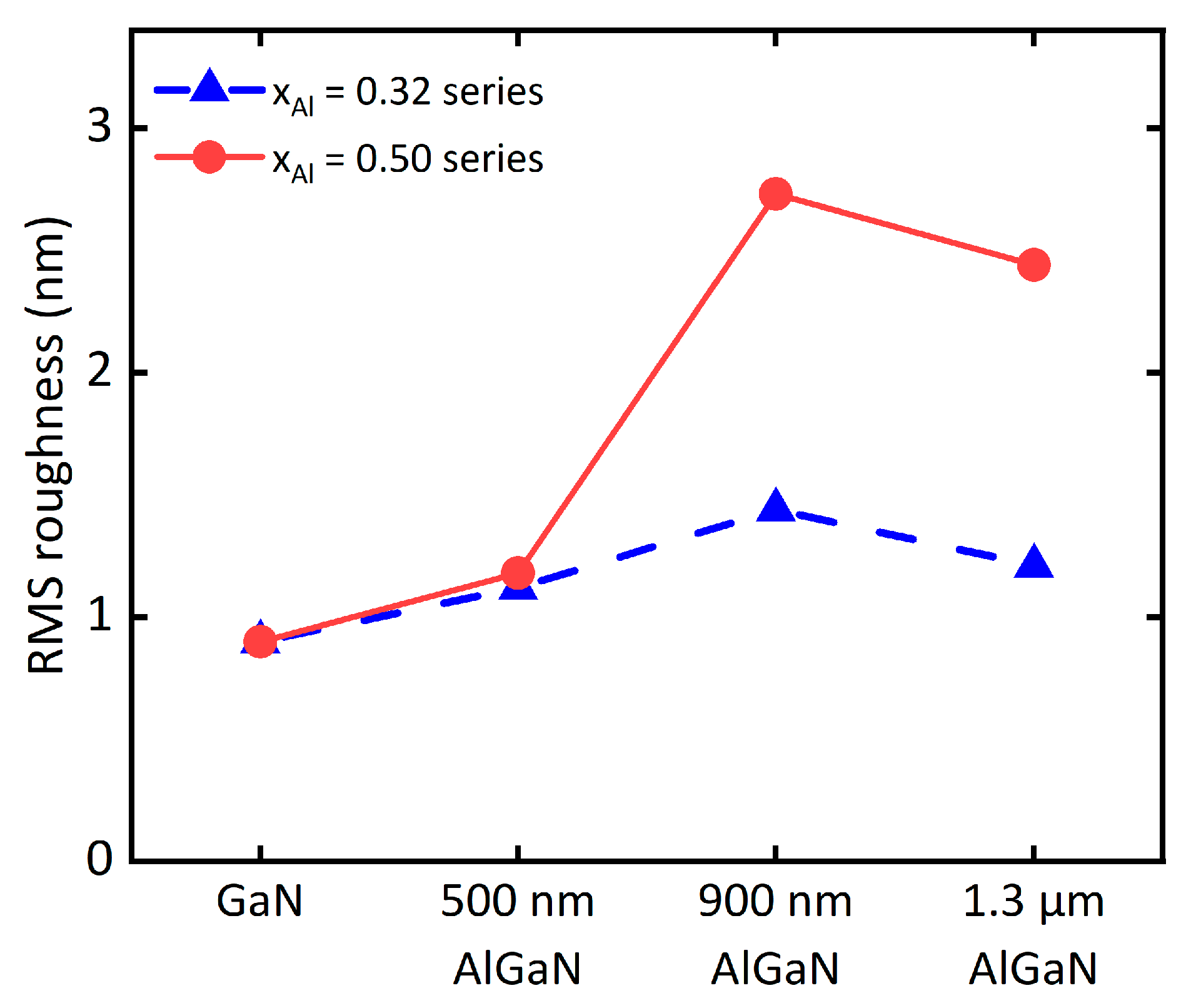
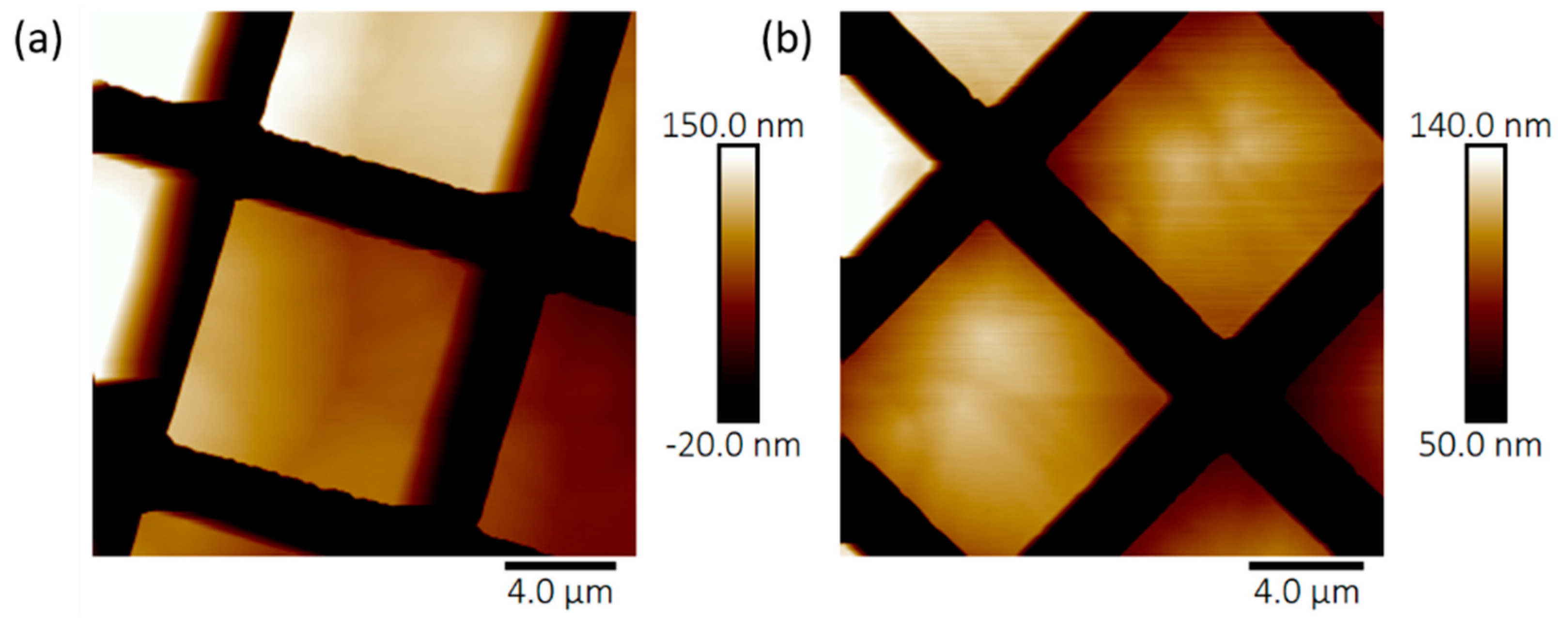
3. Experiment and Results

In the first experiment, the growth was initiated with 10 nm of GaN, which acted as a transition layer before introducing any strain in the structure, followed by 30 nm thick AlGaN layers where the composition was increased in steps with target al. composition (xAl) = 0.05, 0.09, 0.13 and 0.17 at 1080 °C. Afterwards, the temperature was increased to 1155 °C and 30 nm each of AlGaN with target xAl = 0.21 and 0.25 was grown followed by 330 nm of AlGaN with a target al. mole fraction of 0.30. The target xAl was obtained from fully strained AlGaN on GaN calibration samples. The sample was characterized and a further 400 nm of AlGaN was regrown with adjusted TMAl and TMGa flows, so as to decrease xAl and match the lattice constant to the existing epilayer. An additional regrowth was then performed for another 400 nm of AlGaN to bring the total thickness of the AlGaN layer to 1.3 µm. The schematic of the full epitaxial layer structure grown on the pseudo-substrate is shown in Figure 3a.
Evaluation of the initial ~500 nm thick AlGaN structure revealed smooth, crack free layers (Figure 3b) with xAl = 0.35 and a relaxation of ~85%. The increase in measured Al composition over the targeted composition was expected due to the composition pulling effect [40,46,47,48,49,50]. The surface morphology remained smooth after the first and second regrowth (Figure 3c,d respectively). After the first regrowth (which brought the total thickness to ~900 nm), the AlGaN peak corresponded to xAl = 0.32 with ~96% relaxation. The final structure with ~1.3 µm thick AlGaN was fully relaxed and showed xAl = 0.32 (Figure 3e).
With encouraging results having been obtained so far, a second porous PS sample was used to grow AlGaN with a higher xAl, following the structure depicted in the schematic in Figure 4a. A 10 nm GaN transition layer was again grown followed by a step-graded AlGaN layer composed of 25 nm AlGaN layers with target xAl = 0.05. 0.11, 0.17, 0.23, and 0.29 at 1080 °C under nitrogen. As before, the temperature was then increased to 1155 °C and 25 nm AlGaN each with target xAl = 0.35, and 0.41 were grown followed by 325 nm of AlGaN with a target xAl of 0.47 in hydrogen. AFM images demonstrated a smooth surface morphology, and RSM showed an AlGaN peak at xAl = 0.53 with 89% relaxation (Figure 4b). After the solvent was clean and buffered in an HF dip, an additional 400 nm of AlGaN was grown with a slightly reduced TMAl flow to lattice match with the already grown AlGaN layer. The aluminum composition was 50% with 90% relaxation (Figure 4c). A further 400 nm regrowth increased the relaxation to 97% while maintaining the same aluminum content (Figure 4d,e).

4. Discussion

Both the 1.3 µm thick AlGaN samples with xAl = 0.32 and 0.50 showed no signs of any cracking, and were fully relaxed. For the sample with xAl = 0.32, AFM images showed a slight increase in roughness, presented as the root mean square (RMS) value in Figure 5 after the individual regrowth steps. The RMS roughness values increased slightly from 1.1 nm for the first ~500 nm stack to 1.4 nm after the first regrowth and decreased to 1.2 nm after the second regrowth, which is likely due to the AlGaN layer being already fully relaxed. The sample with xAl = 0.50 showed an appreciable increase in roughness with the RMS value rising from 1.2 nm for the initial AlGaN stack to 2.7 nm after the first regrowth (with a total of ~900 nm AlGaN). The second regrowth stage showed no further increase in roughness. While the increase in surface roughness after the first regrowth step was unclear, the circumstance that the roughness did not further increase during the second regrowth suggests that the relaxed underlying AlGaN layer (after the first regrowth) prevented any stress-driven increase in surface roughness in this study, which is often observed when growing strained AlGaN layers.
Further XRD characterization to determine the ω-FWHM of the (002) and ( 2 ¯ 01) reflexes for the sample with xAl = 0.32 showed 418 and 544 arc seconds, respectively, on par with good quality hetero-epitaxial growth [51,52]. Nevertheless, these values were higher than the underlying GaN layer for which ω-FWHM values of ~280 and 386 arc seconds for the (002) and ( 2 ¯ 01) reflexes, respectively, had been recorded. While the somewhat higher FWHM values could be the result of partial plastic relaxation, they could also be caused by local variations in relaxation and in the Al composition, between the edge and center region of an individual tile, or tile to tile variations in the array. In addition, the elastic relaxation process could have led to tile tilt causing an increase in the ω-FWHM values.
For the sample with xAl = 0.50, the (002) ω-FWHM amounted to 385 arc seconds, which was narrower than the value measured for the sample with xAl = 0.32. In contrast, the ( 2 ¯ 01) ω-FWHM increased to 677 arc seconds. This is a much more significant increase compared to the value of 386 arc seconds measured for the GaN base layer and the 544 arc seconds measured for the sample with xAl = 0.32, which may be due to partial plastic relaxation under the formation of edge dislocations. Further investigations are currently underway to clarify the origin of the increase in FWHM, as well as to develop strategies to suppress it.
There was little evidence of growth on the tile sidewalls (Figure 6) which was observed previously when the AlGaN layers were grown with a higher NH3 flow of 178 mmol/min of NH3 [38]. Lower NH3 flow rates are known to suppress lateral growth [53] and could have been the cause for the lack of sidewall growth in this work. Further studies are planned to investigate this aspect, as sidewall growth may allow for tile coalescence to create large-area planar relaxed AlGaN templates.

5. Conclusions

Fully relaxed, crack-free 1.3 µm thick AlGaN layers with xAl = 0.32 and 0.50 were formed on pseudo-substrates composed of 10 × 10 µm2 compliant GaN-on-porous GaN tile arrays. The epilayers were smooth for xAl = 0.32, while an increase in surface roughness and potential onset of partial plastic relaxation were observed for the sample with xAl = 0.50. Further optimization of the step-graded layer and lateral growth can open up a pathway to obtain high quality, large area AlGaN substrates as well as obtain fully relaxed AlGaN with even higher values of xAl.

Author Contributions

Investigation, N.H.; pseudo-substrate processing, H.C., S.S.P. and W.L.; atomic force microscopy, E.K., H.C. and N.H.; writing—original draft preparation, N.H.; writing—review and editing, S.K.; supervision, S.K. and U.K.M.; funding acquisition, U.K.M. All authors have read and agreed to the published version of the manuscript.

Funding

This work was supported by the Office of Naval Research (monitored by Dr. Paul Maki).

Data Availability Statement

The data that support the findings of this study are available within the article. More detailed findings of this study are available from the corresponding author upon reasonable request.

Conflicts of Interest

The authors declare no conflict of interest.

References

  1. Kneissl, M.; Seong, T.Y.; Han, J.; Amano, H. The emergence and prospects of deep-ultraviolet light-emitting diode technologies. Nat. Photon. 2019, 13, 233–244. [Google Scholar] [CrossRef]
  2. Moustakas, T.D.; Paiella, R. Optoelectronic device physics and technology of nitride semiconductors from the UV to the terahertz. Rep. Prog. Phys. 2017, 80, 106501. [Google Scholar] [CrossRef]
  3. Ren, Z.; Yu, H.; Liu, Z.; Wang, D.; Xing, C.; Zhang, H.; Huang, C.; Long, S.; Sun, H. Band engineering of Ⅲ-nitride-based deep-ultraviolet light-emitting diodes: A review. J. Phys. D Appl. Phys. 2019, 53, 073002. [Google Scholar] [CrossRef]
  4. Li, D.; Jiang, K.; Sun, X.; Guo, C. AlGaN photonics: Recent advances in materials and ultraviolet devices. Adv. Optic. Photon. 2018, 10, 43–110. [Google Scholar] [CrossRef]
  5. Song, K.; Mohseni, M.; Taghipour, F. Application of ultraviolet light-emitting diodes (UV-LEDs) for water disinfection: A review. Water Res. 2016, 94, 341–349. [Google Scholar] [CrossRef]
  6. Nagasawa, Y.; Hirano, A. A Review of AlGaN-Based Deep-Ultraviolet Light-Emitting Diodes on Sapphire. Appl. Sci. 2018, 8, 1264. [Google Scholar] [CrossRef] [Green Version]
  7. Sakai, T.; Kushimoto, M.; Zhang, Z.; Sugiyama, N.; Schowalter, L.J.; Honda, Y.; Sasaoka, C.; Amano, H. On-wafer fabrication of etched-mirror UV-C laser diodes with the ALD-deposited DBR. Appl. Phys. Lett. 2020, 116, 122101. [Google Scholar] [CrossRef] [Green Version]
  8. Alkhazragi, O.; Hu, F.; Zou, P.; Ha, Y.; Kang, C.H.; Mao, Y.; Ng, T.K.; Chi, N.; Ooi, B.S. Gbit/s ultraviolet-C diffuse-line-of-sight communication based on probabilistically shaped DMT and diversity reception. Optic Express 2020, 28, 9111–9122. [Google Scholar] [CrossRef] [Green Version]
  9. Vavoulas, A.; Sandalidis, H.G.; Chatzidiamantis, N.D.; Xu, Z.; Karagiannidis, G.K. A survey on ultraviolet C-band (UV-C) communications. IEEE Commun. Surv. Tutor. 2019, 21, 2111–2133. [Google Scholar] [CrossRef]
  10. Zhang, Z.; Kushimoto, M.; Sakai, T.; Sugiyama, N.; Schowalter, L.J.; Sasaoka, C.; Amano, H. A 271.8 nm deep-ultraviolet laser diode for room temperature operation. Appl. Phys. Expr. 2019, 12, 124003. [Google Scholar] [CrossRef]
  11. Drost, R.J.; Sadler, B.M. Survey of ultraviolet non-line-of-sight communications. Semicond. Sci. Technol. 2014, 29, 084006. [Google Scholar] [CrossRef]
  12. Floyd, R.; Hussain, K.; Mamun, A.; Gaevski, M.; Simin, G.; Chandrashekhar, M.V.S.; Khan, A. An initial study of ultraviolet C optical losses for monolithically integrated AlGaN heterojunction optoelectronic devices. Phys. Status Solidi A 2020, 217, 1900801. [Google Scholar] [CrossRef]
  13. Floyd, R.; Hussain, K.; Mamun, A.; Gaevski, M.; Simin, G.; Chandrashekhar, M.V.S.; Khan, A. Photonics integrated circuits using AlxGa1-xN based UVC light-emitting diodes, photodetectors and waveguides. Appl. Phys. Expr. 2020, 13, 022003. [Google Scholar] [CrossRef]
  14. Li, K.H.; Fu, W.Y.; Cheung, Y.F.; Wong, K.K.Y.; Wang, Y.; Lau, K.M.; Choi, H.W. Monolithically integrated InGaN/GaN light-emitting diodes, photodetectors, and waveguides on Si substrate. Optica 2018, 5, 564–569. [Google Scholar] [CrossRef]
  15. Li, K.H.; Cheung, Y.F.; Fu, W.Y.; Wong, K.K.Y.; Choi, H.W. Monolithic integration of GaN-on-Sapphire light-emitting diodes, photodetectors, and waveguides. IEEE J. Sel. Top. Quant. Electron. 2018, 24, 3801706. [Google Scholar] [CrossRef]
  16. Lu, X.; Liu, C.; Jiang, H.; Zou, X.; Zhang, A.; Lau, K.M. Monolithic integration of enhancement mode vertical driving transistors on a standard InGaN/GaN light emitting diode structure. Appl. Phys. Lett. 2016, 109, 053504. [Google Scholar] [CrossRef]
  17. Liu, C.; Cai, Y.; Jiang, H.; Lau, K.M. Monolithic integration of Ⅲ-nitride voltage controlled light emitters with dual-wavelength photodiodes by selective-area epitaxy. Opt. Lett. 2018, 43, 3401–3404. [Google Scholar] [CrossRef] [PubMed] [Green Version]
  18. Chen, D.; Liu, Z.; Lu, X.; Wan, L.; Li, R.; Yang, Z.; Li, G. Efficiency improved by monolithic integration of HEMT with vertical-structure LEDs and Mg doping on dry etched GaN. J. Mater. Chem. C 2019, 7, 2823–2828. [Google Scholar] [CrossRef]
  19. Liu, D.; Cho, S.J.; Park, J.; Seo, J.H.; Dalmau, R.; Zhao, D.; Kim, K.; Gong, J.; Kim, M.; Lee, I.K.; et al. 229 nm UV LEDs on aluminum nitride single crystal substrates using p-type silicon for increased hole injection. Appl. Phys. Lett. 2018, 112, 081101. [Google Scholar] [CrossRef]
  20. Inoue, S.; Tamari, N.; Taniguchi, M. 150 mW deep-ultraviolet light-emitting diodes with large-area AlN nanophotonic light-extraction structure emitting at 265 nm. Appl. Phys. Lett. 2017, 110, 141106. [Google Scholar] [CrossRef] [Green Version]
  21. Bryan, Z.; Bryan, I.; Xie, J.; Mita, S.; Sitar, Z.; Collazo, R. High internal quantum efficiency in AlGaN multiple quantum wells grown on bulk AlN substrates. Appl. Phys. Lett. 2015, 106, 142107. [Google Scholar] [CrossRef]
  22. Lochner, Z.; Kao, T.T.; Liu, Y.S.; Li, X.H.; Satter, M.M.; Shen, S.C.; Yoder, P.D.; Ryou, J.H.; Dupuis, R.D.; Wei, Y.; et al. Deep-ultraviolet lasing at 243 nm from photo-pumped AlGaN/AlN heterostructure on AlN substrate. Appl. Phys. Lett. 2013, 102, 101110. [Google Scholar] [CrossRef] [Green Version]
  23. Xie, J.; Mita, S.; Bryan, Z.; Guo, W.; Hussey, L.; Moody, B.; Schlesser, R.; Kirste, R.; Gerhold, M.; Collazo, R.; et al. Lasing and longitudinal cavity modes in photo-pumped deep ultraviolet AlGaN heterostructures. Appl. Phys. Lett. 2013, 102, 171102. [Google Scholar] [CrossRef] [Green Version]
  24. Martens, M.; Mehnke, F.; Kuhn, C.; Reich, C.; Küller, V.; Knauer, A.; Netzel, C.; Hartmann, C.; Wollweber, J.; Rass, J.; et al. Performance characteristics of UV-C AlGaN-based lasers grown on sapphire and bulk AlN substrates. IEEE Photon. Technol. Lett. 2013, 26, 342–345. [Google Scholar] [CrossRef]
  25. Bondokov, R.T.; Mueller, S.G.; Morgan, K.E.; Slack, G.A.; Schujman, S.; Wood, M.C.; Smart, J.A.; Schowalter, L.J. Large area AlN substrates for electronic applications: An industrial perspective. J. Cryst. Growth 2008, 310, 4020–4026. [Google Scholar] [CrossRef]
  26. Sumathi, R.R.; Gille, P. Development and progress in bulk c-plane AlN single-crystalline template growth for large-area native seeds. Jpn. J. Appl. Phys. 2013, 52, 08JA02. [Google Scholar] [CrossRef]
  27. Ban, K.; Yamamoto, J.; Takeda, K.; Ide, K.; Iwaya, M.; Takeuchi, T.; Kamiyama, S.; Akasaki, I.; Amano, H. Internal quantum efficiency of whole-composition-range AlGaN multiquantum wells. Appl. Phys. Express 2011, 4, 052101. [Google Scholar] [CrossRef]
  28. Reentilä, O.; Brunner, F.; Knauer, A.; Mogilatenko, A.; Neumann, W.; Protzmann, H.; Heuken, M.; Kneissl, M.; Weyers, M.; Tränkle, G. Effect of the AlN nucleation layer growth on AlN material quality. J. Cryst. Growth 2008, 310, 4932–4934. [Google Scholar] [CrossRef]
  29. Ito, K.; Hiramatsu, K.; Amano, H.; Akasaki, I. Preparation of AlxGa1-xN/GaN heterostructure by MOVPE. J. Cryst. Growth 1990, 104, 533–538. [Google Scholar] [CrossRef]
  30. Lee, S.R.; Koleske, D.D.; Cross, K.C.; Floro, J.A.; Waldrip, K.E.; Wise, A.T.; Mahajan, S. In situ measurements of the critical thickness for strain relaxation in AlGaN/GaN heterostructures. Appl. Phys. Lett. 2004, 85, 6164. [Google Scholar] [CrossRef]
  31. Bethoux, J.-M.; Vennéguès, P.; Natali, F.; Feltin, E.; Tottereau, O.; Nataf, G.; De Mierry, P.; Semond, F. Growth of high quality crack-free AlGaN films on GaN templates using plastic relaxation through buried cracks. J. Appl. Phys. 2003, 94, 6499. [Google Scholar] [CrossRef]
  32. Wang, T.; Bai, J.; Parbrook, P.J.; Cullis, A.G. Air-bridged lateral growth of an Al0.98Ga0.02N layer by introduction of porosity in an AlN buffer. Appl. Phys. Lett. 2005, 87, 151906. [Google Scholar] [CrossRef]
  33. Qhalid Fareed, R.S.; Adivarahan, V.; Chen, C.Q.; Rai, S.; Kuokstis, E.; Yang, J.W.; Khan, M.A.; Caissie, J.; Molnar, R.J. Air-bridged lateral growth of crack-free Al0.24Ga0.76N on highly relaxed porous GaN. Appl. Phys. Lett. 2004, 84, 696. [Google Scholar] [CrossRef]
  34. Bergmann, M.A.; Enslin, J.; Yapparov, R.; Hjort, F.; Wickman, B.; Mercinkevičius, S.; Wernicke, T.; Kneissl, M.; Haglund, Å. Electrochemical etching of AlGaN for the realization of thin-film devices. Appl. Phys. Lett. 2019, 115, 182103. [Google Scholar] [CrossRef] [Green Version]
  35. Pasayat, S.S.; Gupta, C.; Wong, M.S.; Wang, Y.; Nakamura, S.; DenBaars, S.P.; Keller, S.; Mishra, U.K. Growth of strain-relaxed InGaN on micrometer-sized patterned compliant GaN pseudo-substrates. Appl. Phys. Lett. 2020, 116, 111101. [Google Scholar]
  36. Huang, S.; Zhang, Y.; Leung, B.; Yuan, G.; Wang, G.; Jiang, H.; Fan, Y.; Sun, Q.; Wang, J.; Xu, K.; et al. Mechanical properties of nanoporous GaN and its application for separation and transfer of GaN thin films. ACS Appl. Mater. Interfaces 2013, 5, 11074. [Google Scholar] [CrossRef]
  37. Fakir, S.; Montagne, A.; Rahmoun, K.; Iost, A.; Ziouche, K. Mechanical properties of porous silicon and oxidized porous silicon by nanoindentation technique. Mater. Sci. Eng. A 2018, 711, 470. [Google Scholar] [CrossRef]
  38. Pasayat, S.S.; Wu, F.; Gupta, C.; DenBaars, S.P.; Nakamura, S.; Keller, S.; Mishra, U.K. Study of pore geometry and dislocations in porous GaN based pseudo-substrates using TEM. IEEE J. Quant. Electron. 2022. [Google Scholar] [CrossRef]
  39. Keller, S.; Pasayat, S.S.; Gupta, C.; DenBaars, S.P.; Nakamura, S.; Mishra, U.K. Patterned III-Nitrides on Porous GaN: Extending Elastic Relaxation from the Nano- to the Micrometer Scale. Phys. Status Solidi RRL 2021, 15, 2100234. [Google Scholar] [CrossRef]
  40. Pasayat, S.S.; Hatui, N.; Li, W.; Gupta, C.; Nakamura, S.; DenBaars, S.P.; Keller, S.; Mishra, U.K. Method of growing elastically relaxed crack-free AlGaN on GaN as substrates for ultra-wide bandgap devices using porous GaN. Appl. Phys. Lett. 2020, 117, 062102. [Google Scholar] [CrossRef]
  41. Zhang, Y.; Ryu, S.W.; Yerino, C.; Leung, B.; Sun, Q.; Song, Q.; Cao, H.; Han, J.A. Conductivity-based selective etching for next generation GaN devices. Phys. Status Solidi B 2010, 247, 1713–1716. [Google Scholar] [CrossRef]
  42. Hatui, N.; Rahman, A.A.; Maliakkal, C.B.; Bhattacharya, A. Direct MOVPE growth of semipolar (11 2 ¯ 2) AlxGa1−xN across the alloy composition range. J. Cryst. Growth 2015, 437, 1–5. [Google Scholar] [CrossRef]
  43. Tang, L.; Tang, B.; Zhang, H.; Yuan, Y. Review—Review of Research on AlGaN MOCVD Growth. ECS J. Solid State Sci. Technol. 2020, 9, 024009. [Google Scholar] [CrossRef]
  44. Pereira, S.; Correia, M.R.; Pereira, E.; O’Donnell, K.P.; Alves, E.; Sequeira, A.D.; Franco, N.; Watson, I.M.; Deatcher, C.J. Strain and composition distributions in wurtzite InGaN/GaN layers extracted from X-ray reciprocal space mapping. Appl. Phys. Lett. 2002, 80, 3913. [Google Scholar] [CrossRef]
  45. Wurm, C.; Collins, H.; Hatui, N.; Li, W.; Pasayat, S.; Hamwey, R.; Sun, K.; Sayed, I.; Khan, K.; Ahmadi, E.; et al. Demonstration of device-quality 60% relaxed In0.2Ga0.8N on porous GaN pseudo-substrates grown by PAMBE. J. Appl. Phys. 2022, 131, 015701. [Google Scholar] [CrossRef]
  46. Kobayashi, A.; Ohta, J.; Fujioka, H. Low temperature epitaxial growth of In0. 25Ga0.75N on lattice-matched ZnO by pulsed laser deposition, J. Appl. Phys. 2006, 99, 123513. [Google Scholar]
  47. Even, A.; Laval, G.; Ledoux, O.; Ferret, P.; Sotta, D.; Guiot, E.; Levy, F.; Robin, I.C.; Dussaigne, A. Enhanced In incorporation in full InGaN heterostructure grown on relaxed InGaN pseudo-substrate. Appl. Phys. Lett. 2017, 110, 262103. [Google Scholar] [CrossRef]
  48. Däubler, J.; Passow, T.; Aidam, R.; Köhler, K.; Kirste, L.; Kunzer, M.; Wagner, J. Long wavelength emitting GaInN quantum wells on metamorphic GaInN buffer layers with enlarged in-plane lattice parameter. Appl. Phys. Lett. 2014, 105, 111111. [Google Scholar] [CrossRef]
  49. Chen, Z.; Pei, Y.; Newman, S.; Brown, D.; Chung, R.; Keller, S.; DenBaars, S.P.; Nakamura, S.; Mishra, U.K. Growth of AlGaN/GaN/AlGaN double heterojunction field-effect transistors and the observation of a compositional pulling effect. Appl. Phys. Lett. 2009, 94, 171117. [Google Scholar] [CrossRef]
  50. Lund, C.; Hestroffer, K.; Hatui, N.; Nakamura, S.; DenBaars, S.P.; Mishra, U.K.; Keller, S. Digital growth of thick N-polar InGaN films on relaxed InGaN pseudosubstrates. Appl. Phys. Express 2017, 10, 111001. [Google Scholar] [CrossRef]
  51. Zhang, Y.; Xing, Z.; Ma, Z.; Chen, Y.; Ding, G.; Xu, P.; Dong, C.; Chen, H.; Le, X. Threading dislocation density comparison between GaN grown on the patterned and conventional sapphire substrate by high resolution X-ray diffraction. Sci. China Phys. Mech. Astron. 2010, 53, 465–468. [Google Scholar] [CrossRef]
  52. Zollner, C.J.; Almogbel, A.; Yao, Y.; SaifAddin, B.K.; Wu, F.; Iza, M.; DenBaars, S.P.; Speck, J.S.; Nakamura, S. Reduced dislocation density and residual tension in AlN grown on SiC by metalorganic chemical vapor deposition. Appl. Phys. Lett. 2019, 115, 161101. [Google Scholar] [CrossRef]
  53. Kapolnek, D.; Keller, S.; Vetury, R.; Underwood, R.D.; Kozodoy, P.; DenBaars, S.P.; Mishra, U.K. Anisotropic epitaxial lateral growth in GaN selective area epitaxy. Appl. Phys. Lett. 1997, 71, 1204. [Google Scholar] [CrossRef] [Green Version]
Figure 1. (a) Schematic structure of the GaN-on-porous-GaN pseudo-substrate. (b) Top view scanning electron microscopy image showing the tiles.
Crystals 12 00989 g001
Figure 2. 5 × 5 µm2 AFM images of AlGaN grown at 1155 °C (a) on 10 × 10 µm2 tiles of compliant pseudo-substrate; (b) on planar GaN, with image taken in the region in between cracks which developed due to strain.
Crystals 12 00989 g002
Figure 3. (a) Schematic of the first structure grown on porous GaN. The xAl is obtained from RSM, and the dashed lines indicate regrowth interfaces. 5 × 5 µm2 AFM height images of (b) initial ~500 nm AlGaN; (c) after first regrowth (corresponding to dtotal ~900 nm AlGaN); (d) after second regrowth (dtotal ~1.3 µm AlGaN) showing good surface morphology. (e) RSM obtained from XRD with the GaN and 1.3 µm AlGaN peaks marked shows that Al0.32Ga0.68N is fully relaxed. The vertical dashed line running up each scan from the GaN peak shows the strain line while the other dashed line is the fully relaxed line.
Crystals 12 00989 g003
Figure 4. (a) Schematic of the second structure grown on porous GaN. The xAl is obtained from RSM, and the dashed lines indicate regrowth interfaces. 5 × 5 µm2 AFM height images of (b) initial ~500 nm AlGaN; (c) after first regrowth (corresponding to dtotal ~900 nm AlGaN); (d) after second regrowth (dtotal ~1.3 µm AlGaN) showing good surface morphology. (e) RSM obtained from XRD with the GaN and 1.3 µm AlGaN peaks marked shows that Al0.50Ga0.50N is fully relaxed. The vertical dashed line running up each scan from the GaN peak shows the strain line while the other dashed line is the fully relaxed line.
Crystals 12 00989 g004
Figure 5. Graph showing the RMS surface roughness for the pseudo-substrate as well as after each AlGaN growth for both xAl = 0.32 and 0.50 samples. For the xAl = 0.32 sample, the roughness remained generally flat, however, it increases after first regrowth for the xAl = 0.50 sample.
Crystals 12 00989 g005
Figure 6. 20 × 20 µm2 AFM height images of 1.3 µm AlGaN grown on 10 × 10 µm2 tiles of compliant pseudo-substrate; with (a) xAl = 0.32 and (b) xAl = 0.50. The 2 µm spacing between the tiles was preserved.
Crystals 12 00989 g006
Publisher’s Note: MDPI stays neutral with regard to jurisdictional claims in published maps and institutional affiliations.

