
Review of Radiation-Induced Effects on β-Ga2O3 Materials and Devices


1
Department of Physics, Indian Institute of Technology Delhi, New Delhi 110016, India
2
Department of Electrical Engineering, Indian Institute of Technology Delhi, New Delhi 110016, India
*
Author to whom correspondence should be addressed.
Crystals 2022, 12(7), 1009; https://0-doi-org.brum.beds.ac.uk/10.3390/cryst12071009
Submission received: 29 January 2022
/
Revised: 5 May 2022
/
Accepted: 19 July 2022
/
Published: 21 July 2022
(This article belongs to the Special Issue Defects in Wide Bandgap Semiconductors)
Abstract
:β-Ga2O3 has become an ultimate choice of emerging new-generation material for its wide range of compelling applications in power electronics. In this review, we have explored the available radiations in the atmosphere and the effects of radiation on the β-Ga2O3 material and devices. The focus in this review summarizes various studies covering different radiation such as swift heavy ions, protons, neutrons, electrons, Gamma, and X-rays to understand the radiation-induced effects on the structure and their reliable performance in harsh environments. In addition, we focused on the various pre-existing defects in β-Ga2O3 and the emergence of radiation-induced defects that provoke a severe concern, especially from the device performance point of view. This review presents the irradiation-induced effects on the devices such as high-power devices such as Schottky barrier diodes (SBDs), field-effect transistors (FETs), metal-oxide-semiconductor (MOS) devices, and photodetectors. Some key studies including the changes in carrier concentration with a removal rate, Schottky barrier height (SBH), ideality factor, defect dynamics dielectric damage, interface charge trapping, a thermally activated recovery mechanism for charge carriers at elevated temperature, and diffusion length of minority charge carriers. These reports show that β-Ga2O3-based devices could be deployable for space or high-radiation terrestrial applications. These results provide/suggest a better device design based on the radiation degradation studies in the state-of-the-art β-Ga2O3 devices.
1. Introduction
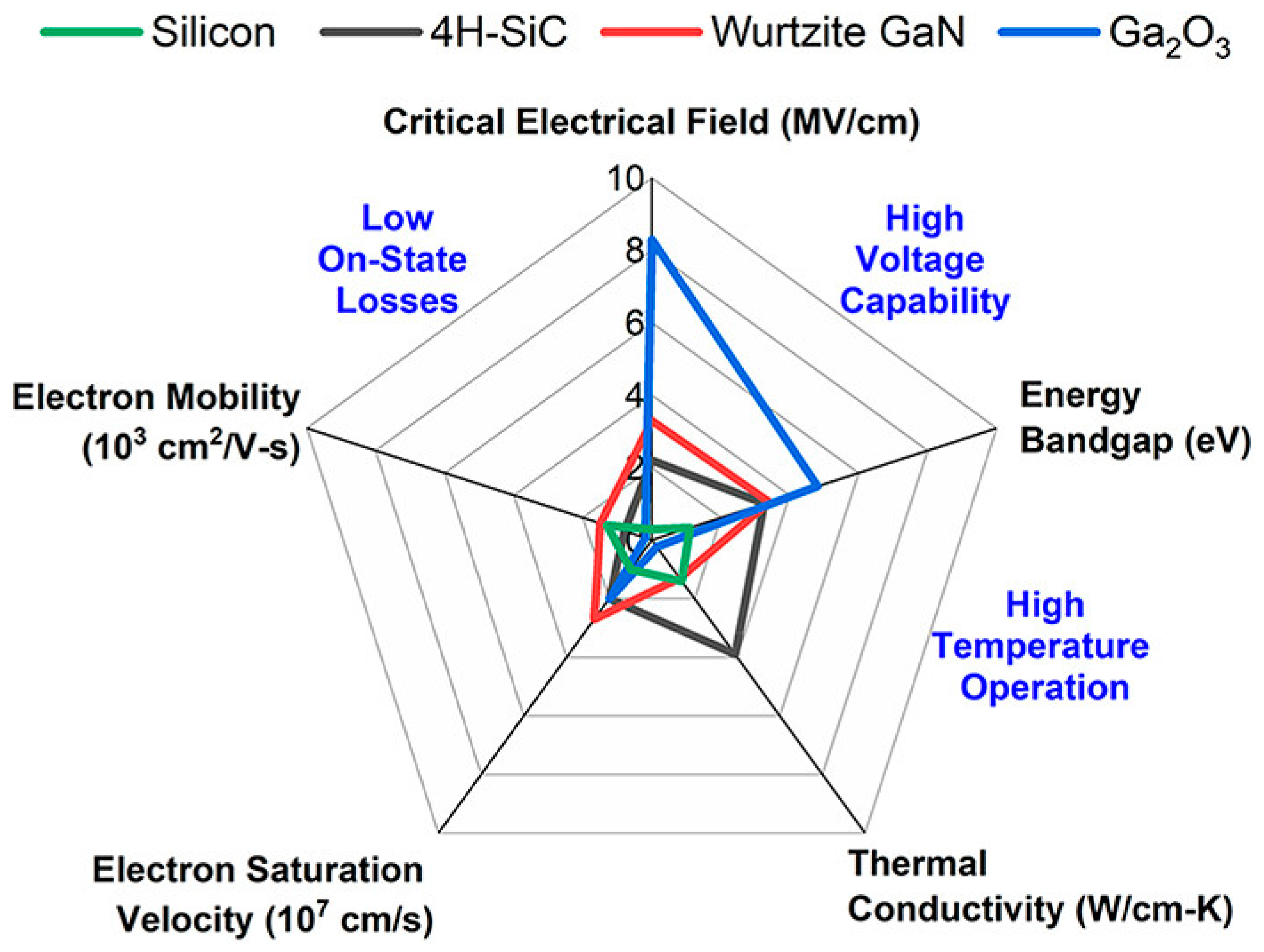
In recent years in the semiconductor industry, substantial advancements in state-of-the-art power devices have yielded a new generation of high-power electronics [1,2]. The Si-based traditional power devices are confronted by high power and high performance [3,4]. In such a scenario, wide bandgap (WBG) semiconductors (bandgap > 3 eV), including SiC and GaN, have garnered significant interest in the recent past [5,6,7,8]. Recently, the focus on Ga2O3 has increased quite significantly. It is treated as one of the most promising WBG semiconductors with adequate mass manufacturing as another successful option due to its conventional melt growth [9,10]. Ga2O3 has phases of α, β, γ, δ, ε, and κ, and amongst these, β-Ga2O3 is the most stable phase. It has a WBG of 4.8–4.9 eV with a high breakdown field of 8 MV/cm, exceeding traditional WBG materials such as SiC (3.3 eV) and GaN (3.4 eV) with a high predicted Baliga’s merit value (BFOM) (see Figure 1) [11,12]. BFOM is a crucial metric for assessing semiconductor materials that can be used in power devices [13,14]. It is about ~3444 for β-Ga2O3, which is much higher than SiC and GaN [15]. With a high 8 MV/cm breakdown field, β-Ga2O3 aim to hold the ultra-high-power device market (>1 MW), surpassing the traditional power electronics [16]. Table 1 summarizes various intrinsic characteristics of β-Ga2O3 and other power device semiconductors.
Over the past two decades, SiC and GaN have started dominating the era of power devices in industrial power markets [5,18,19,20]. However, the technological adoption into space and terrestrial applications is a matter of seeking consistency [21,22]. GaN and SiC-based transistors have shown failure susceptibility at ∼50% of their nominal rated voltage as per the conclusions of space simulations [6,23,24,25,26]. For both SiC and GaN devices, operation in a space environment demonstrated that radiation-induced damage or failure occurs with high and unacceptable leakage currents [23,27,28,29]. In particular, with GaN, there are problems with induced radioactivity with neutron irradiation [30] and the formation of disordered regions [31]. In contrast, with high-energy neutrons, there is an increase in the defect states, which are most probably interstitials [32,33]. High doses of Gamma radiation have also shown significant changes in the device characteristics [30]. In defect test investigations aiming at identifying fundamental material properties, electron irradiation was frequently employed but was not so popular in the deterioration of the devices [34]. Proton irradiation mainly reduces the carrier’s level in GaN owing to the trapping of radiation-induced defect levels and carrier mobility [35]. In addition, high-energy heavy-ion irradiation leads to complex defect formation at the interface and GaN layer [36,37]. Coming to SiC, a high threshold displacement energy of the material results in a high level of radiation hardness compared to other semiconductor materials [38,39]. Photons can produce ionization, generally affecting SiC electronics minimally [40]. In the 4H-SiC Schottky diode exposed to 60Co Gamma rays even up to 100 Mrad (Si), no apparent change was seen in leakage current or signal-to-noise ratio [41]. The experimental results of high-energy protons, neutrons, and electrons effectively lead to displacement damage by creating vacancies, interstitials, and associated defects at high doses [42,43].
Like the extent of SiC and GaN in power electronics, β-Ga2O3 is also becoming a promising candidate [12,44]. So, one needs to understand this newly emerging technology to the extent of SiC and GaN to use this potential material to the full extent, as the development device perspective is at a preliminary stage [45]. Despite significant advances in material development, its unique applications are found in the fabrication of various devices such as high-power Schottky, metal-oxide-semiconductor (MOS) devices, and deep-UV photodetectors [46,47,48,49].
Simple M-S Schottky barrier diodes (SBDs) became the fundamental building block for electronic devices. To advance technological breakthroughs, β-Ga2O3 has been used in certain power devices. Because the Schottky metal and the β-Ga2O3 substrate have different work functions, the substrate is depleted in the β-Ga2O3 SBD rectification process. Thermionic emission (TE) theory governs SBD devices to understand and extract parameters such as SBH and ideality factor [50].
In this equation, J is the current density, is the reverse saturation current density VD = V − IRs corresponds to the voltage drop across the Schottky junction (V denotes the bias voltage and Rs stands for the series resistance), is the ideality factor (a measure of how closely the diode follows the ideal diode equation), q is the electron charge (1.6 × 10⁻¹⁹ C), is the Boltzmann constant (1.38 × 10⁻²³ J/K), T is the temperature, is the SBH (barrier height between the metal electrode and semiconductor), is the Richardson constant, and is the effective mass of the β-Ga2O3 material.
In addition to being an essential application of β-Ga2O3, metal-oxide-semiconductor-field-effect-transistors (MOSFETs) are also a key component of β-Ga2O3 technology. The heart of the MOSFET is the MOS capacitor. Understanding the interface properties between the gate dielectrics and the β-Ga2O3 system is critical to designing and fabricating advanced β-Ga2O3-based MOS devices. In the operation of β-Ga2O3 MOS devices, by applying a positive bias to a gate metal, electrons from the β-Ga2O3 substrate are drawn to the dielectric/β-Ga2O3 interface. Minority carriers (holes) are attracted to the gate dielectric by applying a negative bias. This causes the gate dielectric to change the amount of leakage current that flows through it. The gate tunneling mechanisms such as direct tunneling, Poole–Frenkel (PF) emission, Schottky emission (SE), and Fowler–Nordheim (FN) tunneling processes can be explored. Electrode-limited conduction mechanisms work because of the electrical properties of the metal-dielectric interface.
where, is the current density under direct tunneling, E is the electric field across the oxide, m** is the effective electron mass in the oxide, is the barrier height between conduction bands at the β-Ga2O3-oxide interface, ħ is the reduced Planck constant, and V is the voltage across the oxide.
where JPF is the current density under PF emission, the trap energy level (=), (constant), ε0, and εr represent standard symbols defined as the Boltzmann’s constant, temperature, the permittivity in the vacuum, and the dynamic dielectric constant.
where JSE is the current density under SE, A∗ is the effective Richardson constant.
with, and are known as pre-exponential and exponential factors and have their usual definitions in all other terms.
One of the most important things about these conduction mechanisms, like SE or thermionic emission and FN tunneling, is the height of the metal-dielectric interface barrier (BH). On the other hand, the bulk-limited conduction methods use the dielectric’s electrical properties to help them work. Dielectric films are essential for this conduction process, like PF emission. Therefore, the trap energy level in these films is essential. These methods can be used to obtain information about the trap energy level from dielectric films.
The high critical electric field of β-Ga2O3 enables these devices to function with minimal leakage current at elevated voltages [51]. Understanding irradiation effects on β-Ga2O3 is vital to appraise the device performance and reliability in radiation environments by considering the potential space application of β-Ga2O3-based devices [52,53]. Subsequently, if exposed to space radiation, the performance of devices may deteriorate or even fail; it is imperative to study exploration with a wide range of space radiation. Hence, in this review, we have discussed the radiation-induced effects of radiation in β-Ga2O3 materials and devices, such as swift heavy ions, protons, neutrons, electrons, Gamma, and X-rays [52,53].
2. Defects and Radiation-Induced Defects
Defects in semiconductors play a crucial role and significantly affect the material properties and device characteristics [48]. Most defects are generated during the growth of materials, and some others are induced due to external exposure such as irradiation, ion implantation, etc. [52]. Therefore, an in-depth understanding of β-Ga2O3 defects chemistry and their possible origins is crucial in the single crystal or epitaxial growth scenario to utilize its excellent properties for power device applications.
β-Ga2O3, with a monoclinic crystal structure, has two Ga and three kinds of O lattice sites [44]. The issues of self-compensation, solubility, and defects make it hard todoping in Ga2O3. Experimentally, oxygen vacancies are the deep donors and are not responsible for intrinsic n-type doping in β-Ga2O3 [54]. It has been observed that annealing in an oxygen environment decreases the free-electron density. In contrast, annealing in a nitrogen environment increases the free electron density and improves the n-type conductivity [1]. Hydrogen impurities in interstitial or substitutional oxygen sites are observed as donors and are trapped by acceptor impurities [55]. Theoretically and experimentally, Si, Ge, Sn on the Ga site and F, Cl on the oxygen site are potential shallow donors responsible for intrinsic n-type conductivity [55]. The Sn, Si, and Ge are the widespread dopants for β-Ga2O3 in molecular beam epitaxy (MBE), metal organic chemical vapor phase deposition (MOCVD), and hydride vapor phase epitaxy (HVPE) growth techniques [15,56].
Holes in β-Ga2O3 are self-trapped [54,55]. Theoretically, Zn, Cu, N, and Mg are predicated as acceptors, but they do not increase the p-type conductivity because they are deep defects and do not increase the free holes [57]. Ga vacancies compensate for the n-type conductivity of β-Ga2O3. It has also been observed that O vacancies and Ga vacancies are also responsible for Fermi-level pinning and tuning the work function of β-Ga2O3 in oxygen-deficient and oxygen-rich conditions [58].
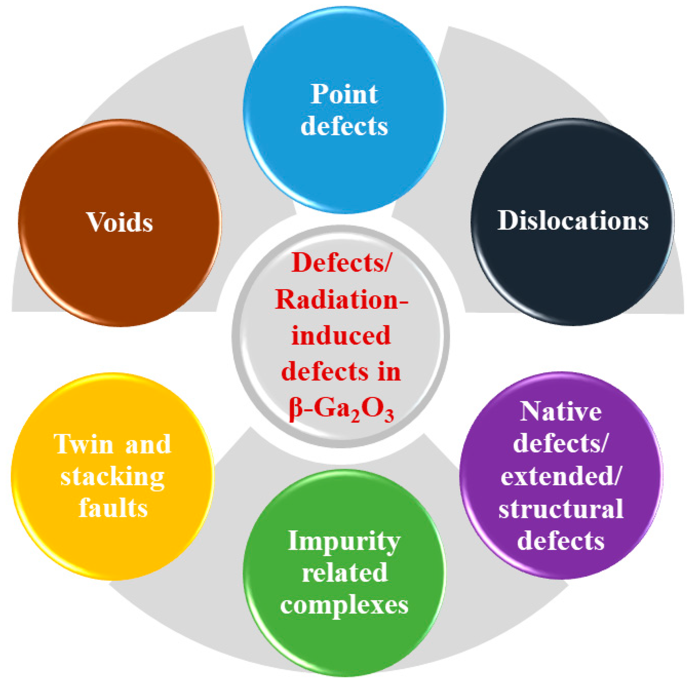
The point defects (impurities, doping, impurity-related complexes), native defects (Ga and O vacancies), and extended structural defects (dislocations, voids, defects originating from voids such as hollow nano-pipes, line-shaped grooves, twin and stacking faults, etc.) are related to the poor device performance [54]. The point defects, impurities, dislocations, and complexes are accountable for poor responsivity, large dark current, noise, and decreases in the efficacy which ultimately shorten the operational lifetime of the UV photodetector devices [59]. In addition, in Schottky barrier diodes (SBDs), it has been found that dislocations and their surroundings are the reason for the undesirable leakage currents [44].
Screw dislocations on the (010) plane and edge dislocation on the (-201) plane of β-Ga2O3 have been reported [60]. The dislocations further produced minor defects, such as arrow-shaped etch pits and gourd-shaped etch pits [61]. The void defects have been observed, including hollow nano-pipes, platelike nano-pipes, nanometer-sized grooves, and line-shaped grooves on different crystal planes of β-Ga2O3 [62].
The point defects, native defects, extended structural defects, and related deep-level defects were investigated by various characterization techniques such as thermally stimulated currents (TSC), deep-level transient spectroscopy (DLTS), and deep-level optical spectroscopy (DLOS). The physical origin of these defects was identified by secondary ion mass spectrometry (SIMS), photoluminescence (PL) and cathodoluminescence (CL), and electron paramagnetic resonance (EPR). In the n-type β-Ga2O3 bulk single crystals grown by Czochralski (CZ), film-fed growth (FEG), etc., various deep-level defects were observed with different concentrations [63]. Their origins were attributed to FeGa, CoGa, and VO and varied impurity incorporation during the growth process. Similar to single bulk crystals, deep-level defects were also observed in epilayers grown by plasma-assisted molecular beam epitaxy (PAMBE), MBE, MOCVD, and HVPE [64]. Their physical origin is attributed to intrinsic defects, vacancies, self-interstitials, and complexes [60]. Various defects and/or radiation-induced defects are shown in Figure 2.
3. Space Radiation
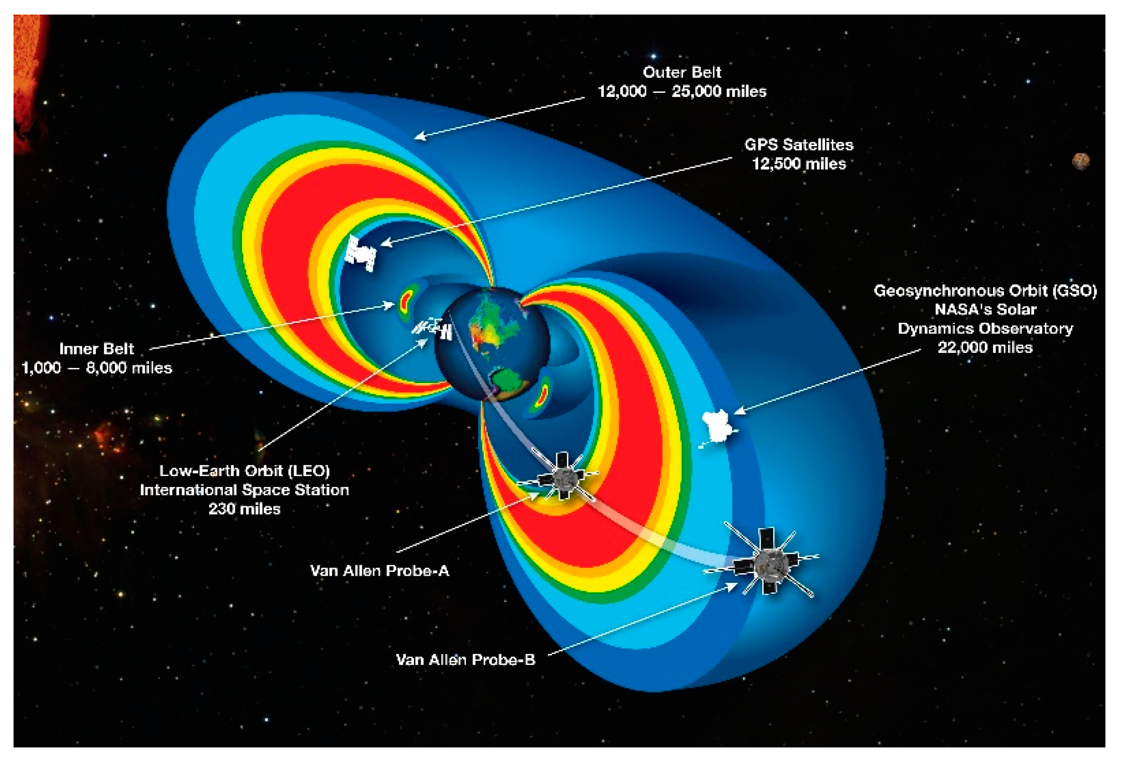
Space radiation is prevalent in the universe exterior to the defensive casing of the Earth’s atmosphere. The radiation we undergo here on Earth is not identical to the radiation in space [65]. Cosmic radiation is composed of particles trapped in the Earth’s magnetic field, and solar flares launched into space and galactic cosmic rays, protons of high energy and heavy ions outside our solar system, which the Earth has captured, as shown in Figure 3 [53]. These sorts of space radiation address ionizing radiation. Inside massive spacecraft constructions, for example, the International Space Station, the primary cosmic beam of around 85% protons and 15% heavy nuclei is partly changed over into secondary neutrons by collisions with the several-grams-each square centimeter of material areal density [53,65]. These secondary neutrons can introduce an extra hazard through electronic materials’ single-event effects (SEEs).
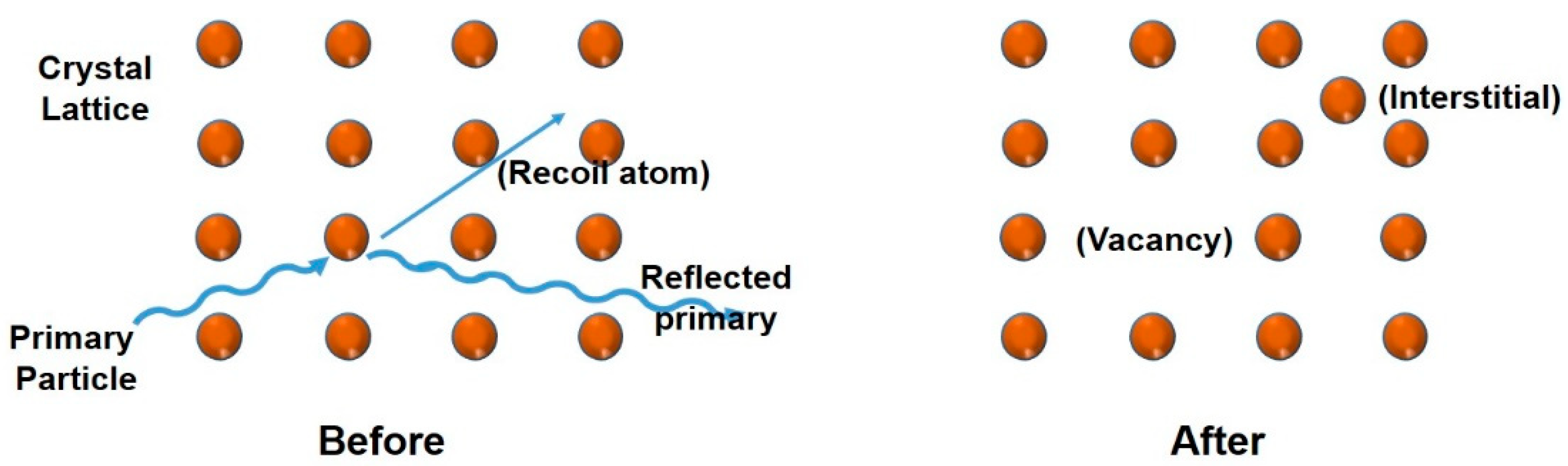
Although the Sun generates various types of electromagnetic radiation, the more significant one encompasses visible, infrared, and UV radiation. Incidentally, massive explosions termed solar flares happen outside the Sun and deliver an enormous amount of energy out into space as X-rays, Gamma rays, and surges of protons and electrons. Such highly intense solar flares can severely affect space travellers and their gear. Usually, the dose rate in the space environment ranges from ~10−4 to 10−2 rad/s (1 gray = 1 J/kg = 100 rad), which is low compared to the dose rates considered on the lab scale. However, the materials exposed to such a space environment for years may cause total ionizing dose (TID) levels in 105 rad. The ionizing doses absorbed by the semiconductor materials such as Si, GaAs, and Ga2O3 are measured in rad or gray (Gy). The radiation particles primarily consist of neutrons, protons, and electrons, which cause the atoms or ions displacement from the crystal lattice of the materials [66], as shown in Figure 4.
4. Radiation Damage in Ga2O3
4.1. Heavy Ions (Protons and SHI)
4.1.1. Heavy Ions
The literature is relatively sparse about the irradiation effects on β-Ga2O3 using swift heavy ions (SHIs) [67,68]. The SHI irradiation-induced effects are pertinently different from electrons, protons, neutrons, X-rays, and γ-rays [69,70,71]. Tracy et al. investigated radiation response through in situ X-ray diffraction of β-Ga2O3 using 946 MeV Au ions up to 1 × 10¹³ ions/cm2 with the latent track cross-sectional area estimated as 54 ± 5 nm2 [72]. The energy loss mechanisms are quite important to understand the interaction of the energetic ion when traversed through any target substance. The electronic (Se) and nuclear energy (Sn) loss mechanisms are liable for the irradiation-induced effects. In these two mechanisms, Se governs when the energy of the ion is >1 MeV/u, whereas Sn leads at <1 keV/u [73]. Ion-solid interactions generate defects predominantly via atomic displacement within any material because of atomic excitation and ionization [74]. Nevertheless, the following relaxation of these atomic displacements happens in picoseconds time [36]. With an increase in the fluence of the ion, the enhancement in the creation of defects leads to increasing the number of trapping centers, ultimately resulting in variation of electrical parameters.
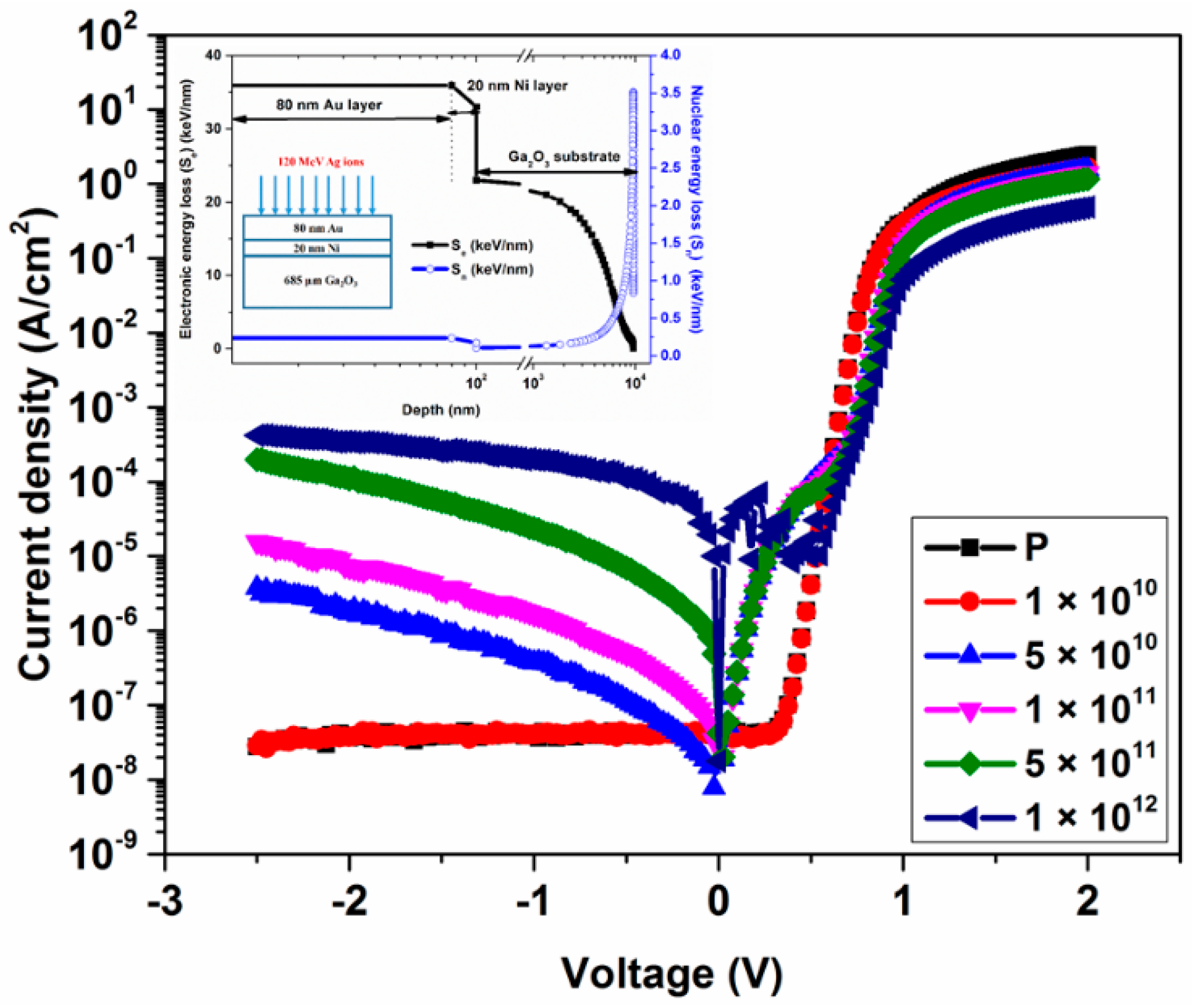
Recently, Manikanthababu et al. reported in situ 120 MeV Ag7+ SHI irradiation on Ni/β-Ga2O3 vertical SBDs [75] (as shown in Figure 5). The stopping and range of ions in matter (SRIM) simulations show that the Se value dominated the Sn value by two orders (see Figure 5 (inset)). The irradiation-induced degradation at the ion fluences ranges from 1 × 10¹⁰ ions/cm2 to 1 × 10¹² ions/cm2, as was observed. The leakage current density is four orders higher between the pristine and highest fluence at −1 V, whereas the series resistance value increased from 3.38 × 10³ to 1.15 × 10⁴ Ω. The estimated ΦB decreases from 1.11 to 0.93 eV, and the η rises from 1.16 to 2.06. XPS measurements of Ga 3d core levels revealed that Ga3+ and Ga2+ peak positions are at around 20.2 eV and 19.9 eV, which remain the same before and after ion irradiation, except there was a variation in the intensity and width. Conversely, the changes observed in the intensity and peak width of O(II) are substantial at the highest fluence. These results show that the surface adsorbed or lattice oxygen increases, which leads to the formation of GaO.
4.1.2. Protons
M. E. Ingebrigtsen et al. studied proton irradiation on β-Ga2O3 with energies 0.6 and 1.9 MeV at 5 × 10⁹ ions/cm2 to 6 × 10¹⁴ ions/cm2 ion fluences to understand the effect on carrier concentration and defects dynamics [76]. At 2 × 10¹³ ions/cm2 and above fluences, there was a comprehensive elimination of free charge carriers, while less or no impact was found under 6 × 10¹² ions/cm2 fluence. Studies at higher temperatures showed a thermally activated recovery mechanism for charge carriers. The recovery energy activation takes place in second order at ~1.2 eV. Experimental observations and theoretical calculations suggested that Ga interstitial, vacancy, and antisite may explain the removal from the charge carrier of Fermi-level pinning from the conduction band minimum (CBM). Migration can, however, be owing to subsequent VGa passivation using H-derived or VO defects accountable for recovery. The DLTS indicated that two deep levels are generated at energy locations of approximately 0.75 and 1.4 eV below the CBM. The latter vanishes from these two levels following the initial DLTS measurements, whereas the former rises in concentration. These findings concluded that these levels’ formation is more probable because of a defect complex.
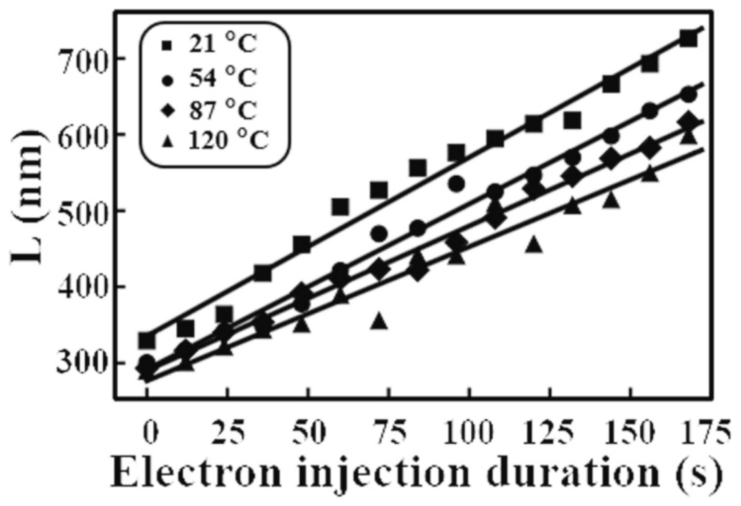
Sushrut Modak et al. reported the impact of protons with an energy of 10 MeV Si-doped β-Ga2O3 Schottky diodes at a fluence of 1 × 10¹⁴ ions/cm2 [77]. The diffusion length (L) of minority charge carriers decreases from 330 nm at 21 °C to 289 nm at 120 °C within a range of ~26 meV activation energies corresponding to a low Si trap level (see Figure 6). A more extended electron beam exposure period improves L at room temperature from 330 nm to 726 nm. L’s rise is reduced with an activated energy of ~43 meV at higher temperatures.
4.2. Neutrons
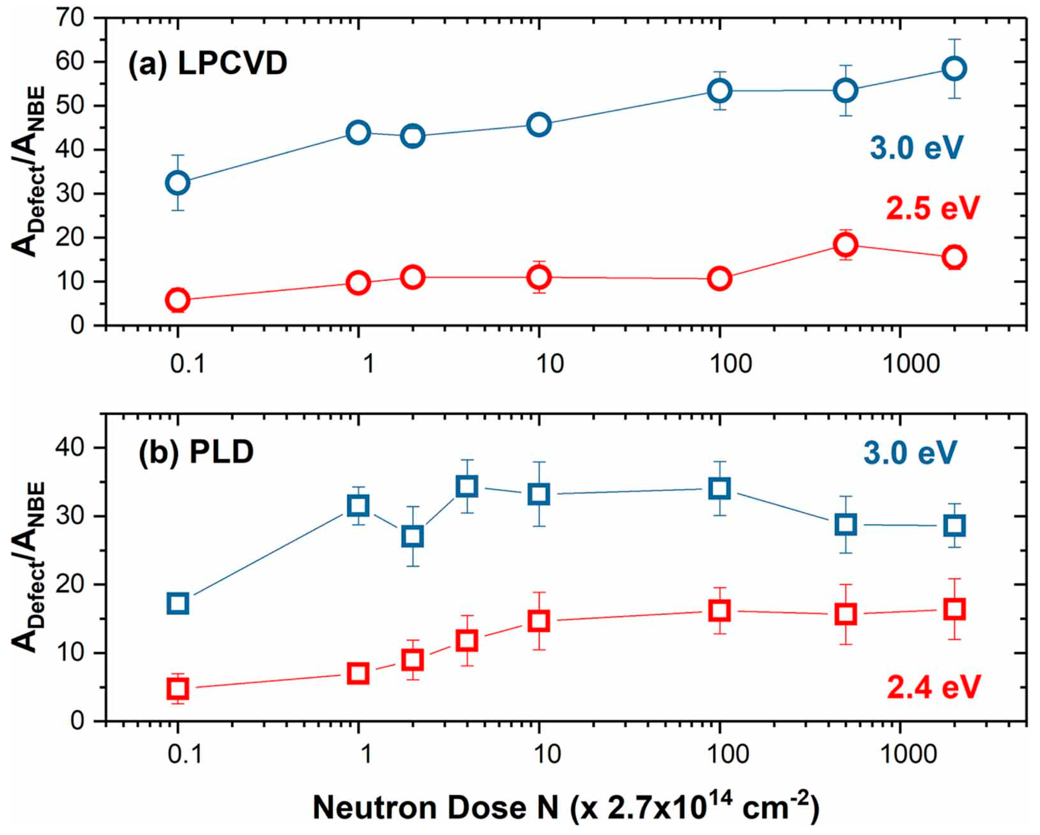
A recent report investigated the impact of near-surface plasma processing and neutron irradiation on the defects present at the surface of low-pressure chemical vapor deposition (LPCVD)-grown β-Ga2O3 samples. These samples were analyzed using depth-resolved cathodoluminescence spectroscopy (DRCLS) and surface photovoltage spectroscopy [78]. The studies from the aforementioned optical techniques facilitated the analysis of spectral changes correlated with the removal or creation of defects due to O and Ga vacancies associated with energy levels in β-Ga2O3. In addition, various doses of neutrons at different temperatures in forming gas atmospheres were also studied on pulsed laser deposition (PLD) and LPCVD-grown β-Ga2O3. The spectral changes at three deep level defects, such as 3.5 to 2.5 eV, were observed by DRCLS and correlated with electrical properties measured using the temperature-dependent Hall system. FG anneal studies revealed that the VGa defect passivation can be conducted without dissociating VGa-H complexes at higher temperatures, which furnished an approach to recover the induced damage. In Figure 7, the peaks 2.4 to 3.0 eV are highlighted for both LPCVD- and PLD-grown Ga2O3 samples [79].
An investigation was reported on the effects of neutron irradiation on β-Ga2O3 SBDs [80]. Using DLOS and DLTS analysis, a decrease was found in the carrier concentration due to irradiation, which formed the defects in the bandgap. The pulsed neutron irradiation effect on HVPE-grown Si-doped n-type β-Ga2O3 films on bulk Sn-doped n+ β-Ga2O3 substrates resulted in linear increment with neutron fluence and the trap concentration. The density of deep electron traps was as follows: E2* (Ec—0.74 eV), E3 (Ec—1.05 eV), and E4 (Ec—1.2 eV), with an acquaintance rate close to 0.4—0.6 cm−1, while the density of the E2 traps (Ec—0.8 eV) identified with Fe was essentially unaltered. There was a decrement in diffusion length from 0.16 μm to 0.12 μm due to irradiation-induced recombination-active electron and hole traps. This was not very effective in β-Ga2O3 when compared to GaN. The E2* and E3 centers are associated with O or Ga vacancies [80].
4.3. Electrons
The impact of electron injection on Si-doped MOCVD-grown β-Ga2O3 and Si-doped HVPE-grown β-Ga2O3 epilayers was studied using electron beam irradiation in a scanning electron microscope (SEM) [78]. The Si-doped MOCVD-grown β-Ga2O3 epilayer was irradiated upon electron injection using a 30 kV electron beam of SEM. The near band emission (NBE) was observed using variable temperature CL characteristics attributed to non-equilibrium carrier recombination. In the case of electron beam irradiation on Si-doped HVPE-grown β-Ga2O3 epilayer, using 10 kV electron of SEM and in situ electron beam-induced current (EBIC) and cathodoluminescence (CL) techniques revealed non-equilibrium electron-hole pair generation in β-Ga2O3. An increment in minority carrier diffusion length and minority carrier transport was observed and attributed to increased non-equilibrium hole lifetimes in the valence band of n-type Ga2O3.
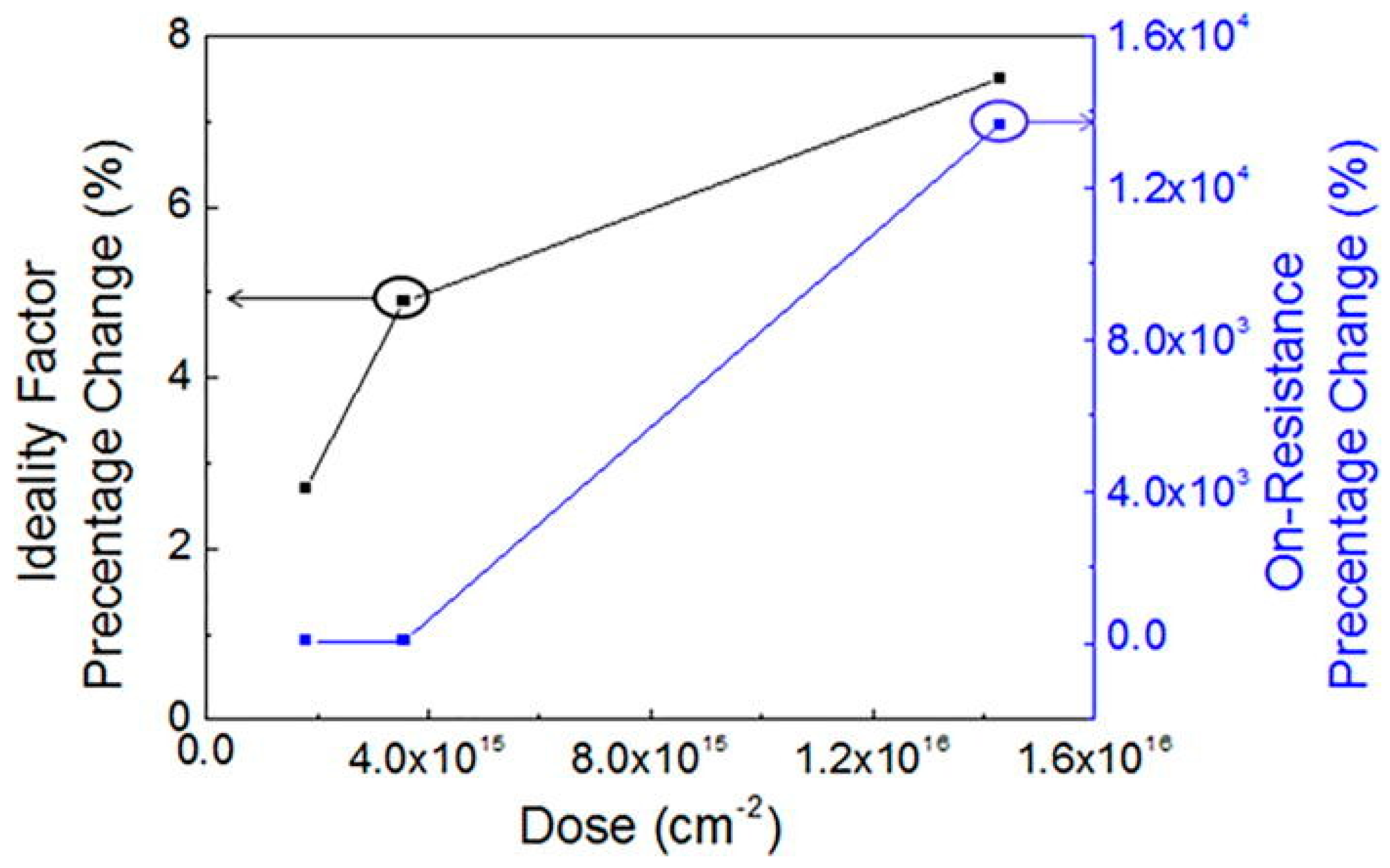
The diodes were fabricated using Si-doped n-type Ga2O3 grown on β-phase Ga2O3 single crystal substrate by HVPE [81]. The fabricated Ga2O3-based diodes underwent electron irradiation for different fluence, and the beam current was maintained close to 10−3 A. The electrical properties were studied, which showed a decrease in carrier concentration with a removal rate of 4.9 cm−1. An increment in the η of ~8% at the highest fluence is observed when carrying out the 2 kT region of the forward I-V data, whereas a decrement for reverse bias current with respect to electron fluence is observed. The increment in ideality factor of the diode and Ron with ascending electron fluence is observed (see Figure 8). There is little change in the reverse recovery characteristics even at the highest fluences, whereas the on/off ratio is diminished [81].
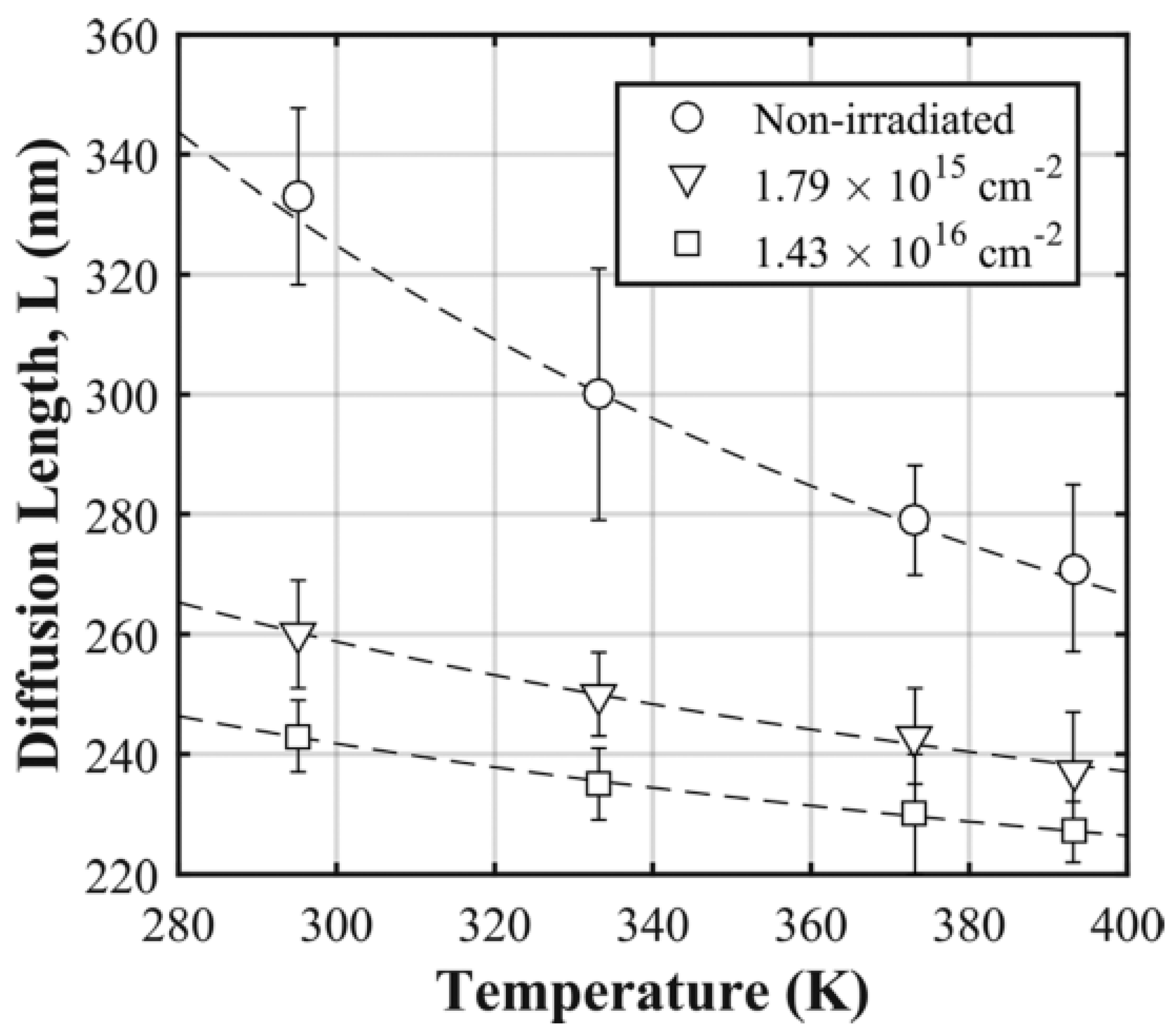
J. Lee et al. reported on a vertical Schottky rectifier irradiated with 1.5 MeV electrons at various fluences [82]. As a function of temperature, the minority hole diffusion was found by utilizing the electron-beam-induced current technique for each irradiation dose. The results for diffusion length vs. temperature according to fluences are shown in Figure 9. The activation energy (Ea) is reduced by 18.1 meV and is reduced further to 13.6 meV for higher irradiation doses, whereas for non-irradiated samples, the Ea is 40.9 meV. In response to the irradiation, there is a rise in recombination rate, and it is also confirmed by the decay lifetime of the sample using time-resolved cathodoluminescence. The decay lifetime for non-irradiated samples is 210 ps, which is reduced for irradiated samples to 151 and 138 ps [82].
4.4. Gamma and X-rays
4.4.1. Gamma
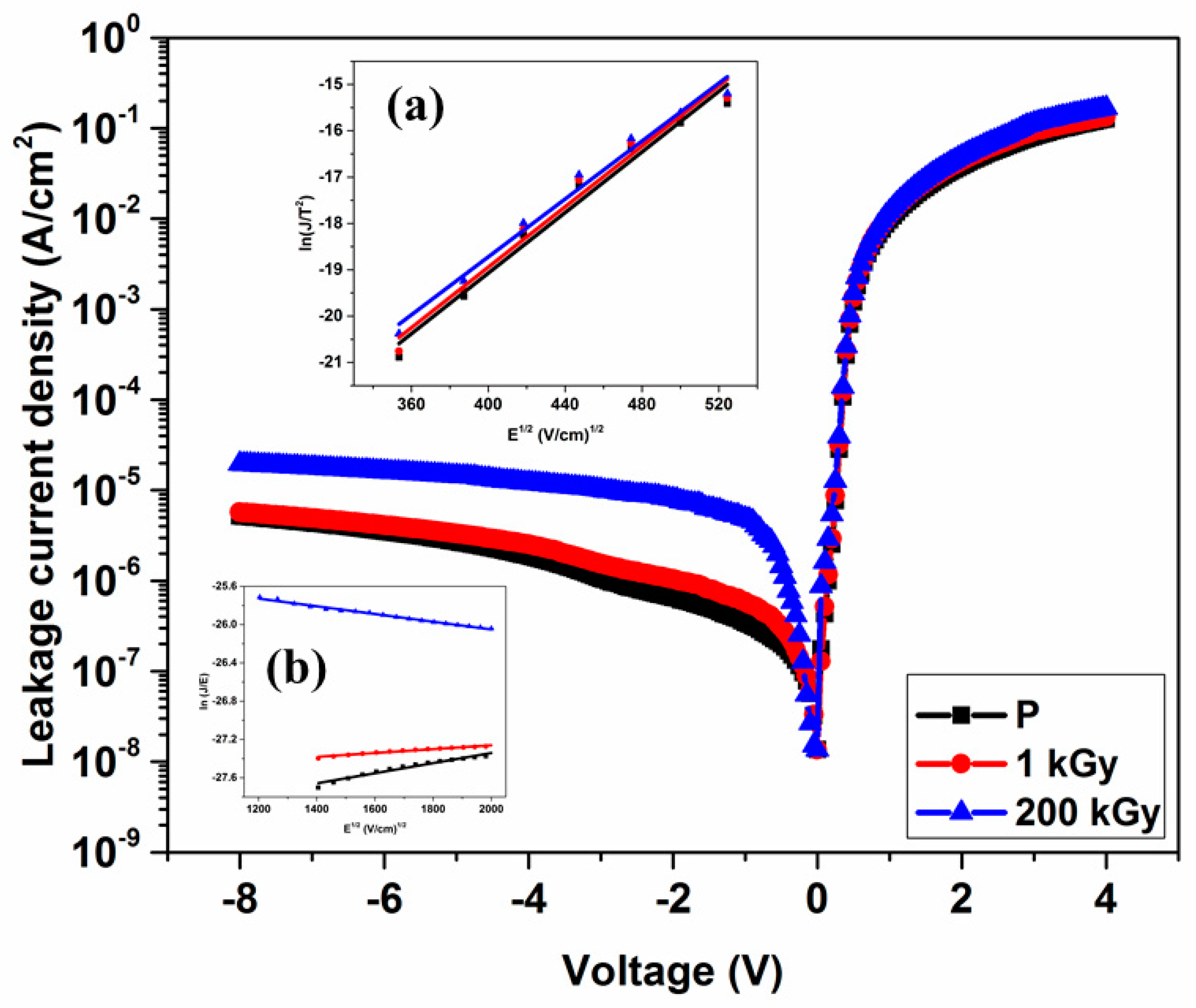
A few authors examined the Gamma-ray tolerance of β-Ga2O3 devices, including solar-blind photodetector, MOSCAP, MOSFET, and Schottky barrier diodes [53]. Yang et al. observed minimal changes in Schottky barrier diode parameters on exposure of 100 kGy (Si) dose of Gamma-ray irradiation on Schottky barrier diodes fabricated on HVPE-grown Ga2O3 epilayer [83]. The changes in carrier concentration at the doses employed are small enough that the rectifier properties do not degrade very much. These experimental evidences were found to be in line with fabricated Ga2O3 MOSFETs [83]. In 2018, Wong et al. reported that epitaxial Ga2O3 MOSFET exhibited little change in output current and threshold voltage and high radiation tolerance to bulk defect generation at a very high dose of 1.6 MGy (SiO2) [84]. These changes were attributed to dielectric damage and interface charge trapping rather than any difference in intrinsic radiation hardness of the Ga2O3 epilayer [84]. Tak et al. studied the Gamma-ray irradiation on a solar-blind photodetector fabricated on PLD-grown β-Ga2O3 thin film on the sapphire substrate [85]. The dark current was found to be increased with the increase of exposure up to 100 kGy. In contrast, the photo-to-dark current ratio and Schottky barrier height (SBH) were raised with exposure up to 100 kGy. In 2020, Manikanthababu et al. studied the Gamma-ray exposure on HfO2/β-Ga2O3 MOSCAPs fabricated on HVPE-grown β-Ga2O3 to reveal the effect on HfO2-based gate dielectrics in MOS devices [86]. It was observed that SBH decreased and leakage current increased upon exposure up to 200 kGy as shown in Figure 10. Schottky emission may be caused by the charging trapping in HfO2. The calculated SBH values were estimated as 0.95 eV, 0.86 eV, and 0.83 eV for the pristine, 1 kGy, and 200 kGy, respectively (see Figure 10a). The increase in leakage current ascribed to an increase in oxide traps and interface traps caused the charge-trapping and the trap-assisted Poole–Frenkel (PF) tunneling mechanism (see Fitted ln(J/E) vs. E1/2 plot in Figure 10(inset 10b)). So, the changes that occurred in β-Ga2O3-based devices are owing to a process dependent on fabricating devices and the quality of the dielectrics, which implies high radiation hardness of single crystal β-Ga2O3.
4.4.2. X-rays
X. Lu et al. demonstrated the SBDs-based X-ray detector fabricated on (100) EFG-grown β-Ga2O3 single crystal [4]. The X-ray detector exhibited a high photo-to-dark current ratio of 800 at the reverse bias of -15 V and a dose rate of 1.5 Gy/s at a 1 cm distance from the source. It was attributed to the low leakage current of the SBD. The detector showed an excellent transient response with different X-ray dose rates. Due to the significant penetration depth of X-ray in β-Ga2O3 over 100 µm, two other mechanisms, photovoltaic in the space charge region and photoconductive in the natural region, were attributed to the fast and slow response of the X-ray detection at a reverse bias of −15 V. However, at zero bias, the detector showed perfect photovoltaic characteristics. Bhuiyan et al. explored the effect of X-ray irradiation in Al2O3/β-Ga2O3-based MOS capacitors [87]. Increased hole traps were observed under positive bias conditions for devices irradiated with 10 kV X-rays at a dose rate of 31.5 krad min−1 (SiO2). A shift in flat-band voltage under 10 kV X-ray irradiation was attributed to the oxygen vacancies in Al2O3. The annealing in N2 ambient was extremely useful in reducing defect density and improving device reliability and radiation response. The influence of high-energy X-rays radiation on mechanically exfoliated quasi-2D β-Ga2O3 nanoflake FETs was investigated [88]. It was observed that at low ionizing doses (<240 krad), the photo-effect affected the device’s performance, and the subsequent persistent photocurrent effect was attributed to the pre-existing electron traps in the oxides far away from the SiO2/β-Ga2O3 interface. At higher doses of more than 240 krad, the X-ray irradiation-induced structural or compositional deterioration, and newly generated electron traps exist at the interface of SiO2/β-Ga2O3.
5. Future Perspectives
Since β-Ga2O3-based power electronics are still in the infancy stage, a thorough investigation is further essential to tune the material properties to use the full extent of this material, which aids the effective device design in harsh environments. A reasonable amount of work on the radiation hardness of β-phase Ga2O3 is reported. As a result, many efforts may be devoted to the other stable phases such as α, γ, δ, ε, and κ. Therefore, the device perspective of these phases is essential to begin with, and later must be devoted to the radiation hardness of these Ga2O3 phases. A more in-depth study of these phases is required in order to investigate the physical, electrical, and thermal properties of Ga2O3 since there is still a great deal of potential remaining in Ga2O3.
p-type doping in Ga2O3 has been deemed difficult, due to its wide bandgap even though some reports are available in the literature. Only deep acceptors (activation energies more than 1 eV) have been reported for undoped and doped materials where acceptor ionization has been significantly low at room temperature. In such a consequence, monoatomic H with low formation energy looks to be promising, as it has the capability of occupying both the interstitial and substitutional sites to be had as a donor. On the other hand, Cu and N impurities that were predicted to cause defect levels deep in the Ga2O3 bandgap act like p-type dopants. A thorough and experimental realization of these theoretical predictions is necessary to explore the maximum potential of Ga2O3.
Heavy ion irradiation, especially dealing with a few MeV to hundreds of MeV on the β-Ga2O3 devices, needs to be greatly explored. There are very few reports investigating the device perspective. Moreover, the well-known Ni/Au Schottky contacts were used so far. However, these contacts degraded, and the barrier height was tremendously lowered. So, these contacts can be replaced with other contacts with a larger barrier height. This step increases the barrier heights and limits the reverse leakage currents. In addition, low-energy (few keV) ions can also be used to tune the material properties without changing the phase of the Ga2O3. More investigations are required with different ion species, and induced defect dynamics can be explored.
The proton-irradiation-induced vacancies, point defects, and interstitials significantly impact the structural and electrical characteristics of the Ga2O3 devices. The M-S interface is confronted with the problem of Fermi level pinning in such a process. To control such kinds of effects is a challenge. It requires some investigation to learn how to manage such an impact so that the consequences of pure proton irradiation can be investigated. To properly identify the numerous individual defect levels or defect complex levels caused by proton irradiation, rigorous theoretical estimates and experimental confirmation must be followed by further investigation.
Neutron irradiation causes substantial carrier reduction due to defects within the Ga2O3 conduction band. Neutron-irradiation-induced defect annealing is also possible in the Ga2O3-based devices. Exploring this effect with low fluences or low energy irradiation in optimized conditions enables the essential step of lowering the pre-existing defect states. This may improve the device’s performance.
The limited literature on electron irradiation of Ga2O3 devices can be extended with various dopants. The existence of shallow donor levels with traditional Si dopants should be minimized. These shallow donor levels definitely aid the leakage current and reduction of the efficient device properties. This can be achieved by optimizing the growth techniques with certain dopants to properly tune the activation energies and minimize the carrier reduction. Similar to neutron irradiation, the irradiation-induced annealing may be carefully investigated to understand the repair process of irradiation-induced defect dynamics.
Gamma-ray irradiation on various β-Ga2O3 devices was explored. The Gamma doses of a few Mega gray could not degrade the performance of β-Ga2O3 devices. However, the Gamma-irradiation-induced defects within the β-Ga2O3-based MOS devices have pertinent effects, as the dielectric was greatly affected. The gate dielectric with more efficient radiation resistance than SiO2 may be used to obtain more radiation tolerance.
The critical doses can be tested and optimized with various X-ray energies. It helps to find out the X-ray-irradiation-induced structural effects and emerging traps. The newly generated defects may affect mobility. These traps at the β-Ga2O3/gate dielectric interface can increase coulomb scattering and thus lower mobility. Such degradation can significantly impact the device/circuit performance and therefore needs to be minimized through the optimization process in the future. So, it is quite necessary to reduce the coulomb scattering so that the mobility of the conduction electrons can be increased. Consequently, a discontinuity of the conduction band is needed to create a thin channel where the high-density electrons can exist, and the electrons in the channel can be separated from their donor atoms, which reduces coulomb scattering and increases the mobility of the conducting electrons. Therefore, many electrons can accumulate within a thin channel with high mobility.
Finally, understanding the effects of radiation on Ga2O3 materials and devices is very important from the technological and fundamental study point of view. The response of Ga2O3 devices towards different types of radiation will govern the application of these devices in radiation environments such as outer space, nuclear reactors, and accelerator laboratories. So, in the future, more detailed investigations need to be carried out in this direction so that the radiation hardness of Ga2O3 materials and devices can be ascertained and established. Using theoretical and experimental approaches, it will also be helpful to understand various defects created in Ga2O3 due to irradiation and their electronic, optical, and structural properties. So, studying the effect of irradiation on Ga2O3 materials and devices will be a vibrant and dynamic area of research in the coming years and holds a lot of potential from the application standpoint.
6. Conclusions
In this review, we have presented a brief account of recent studies related to radiation effects such as swift heavy ions, protons, neutrons, electrons, Gamma, and X-rays on β-Ga2O3-based devices. SHI-irradiation-induced degradation reflects four significant orders of increased leakage current density, SBH decrease, and the ideality factor rise in Ni/ β-Ga2O3 vertical Schottky diodes. XPS measurements of Ga 3d and O 1s core levels revealed that there is an increase in the Ga and O defects after SHI ion irradiation. Proton irradiation on both bulk and epitaxial layers of β-Ga2O3 above a fluence of 2 × 10¹³ ions/cm2 exhibited a complete removal of free charge carriers, and there was less impact on the lower fluences. Coming to neutron irradiation, there was a decrease in diffusion length from 0.16 μm to 0.12 μm due to irradiation-induced recombination-active electron. SBD and MOSFET devices on exposure to 100 kGy (Si) dose of Gamma-ray irradiation showed small carrier concentration changes, and the device degradation was not very significant. The X-ray detector with a high photo-to-dark current ratio of 800 at the reverse bias −15 V and low leakage currents implies an excellent transient response. In Al2O3/β-Ga2O3 MOS devices, a shift in flat band voltage under 10 kV X-ray irradiation was credited to the O vacancies in Al2O3. Reduced defect density and improved device durability and radiation response were enhanced by annealing in N2 ambient.
Author Contributions
Writing—original draft, N.M., H.S. and P.S.; writing—review and editing, R.S. All authors have read and agreed to the published version of the manuscript.
Funding
This research was funded by the Department of Science and Technology (DST), India; partial financial support for this work was provided under BRICS Cooperation scheme (DST/IMRCD/BRICS/Pilot Call 3/GaO-Nitrides/2019) with grant number RP04000G.
Institutional Review Board Statement
Not applicable.
Informed Consent Statement
Not applicable.
Data Availability Statement
Data can be shared upon direct request.
Acknowledgments
R.S. acknowledges the Department of Science and Technology (DST), India, for partial financial support for this work under BRICS Cooperation scheme (DST/IMRCD/BRICS/Pilot Call 3/GaO-Nitrides/2019). NMB is grateful to DST, India, for the financial support from the BRICS project. H.S acknowledges the Council of Scientific and Industrial Research (CSIR) for providing research fellowship.
Conflicts of Interest
The authors declare no conflict of interest.
References
- Pearton, S.J.; Yang, J.; Cary, P.H.; Ren, F.; Kim, J.; Tadjer, M.J.; Mastro, M.A. A review of Ga2O3 materials, processing, and devices. Appl. Phys. Rev. 2018, 5, 011301. [Google Scholar] [CrossRef] [Green Version]
- Jones, E.A.; Wang, F.F.; Costinett, D. Review of Commercial GaN Power Devices and GaN-Based Converter Design Challenges. IEEE J. Emerg. Sel. Top. Power Electron. 2016, 4, 707–719. [Google Scholar] [CrossRef]
- Chen, K.J.; Haberlen, O.; Lidow, A.; Tsai, C.L.; Ueda, T.; Uemoto, Y.; Wu, Y. GaN-on-Si Power Technology: Devices and Applications. IEEE Trans. Electron Devices 2017, 64, 779–795. [Google Scholar] [CrossRef]
- Chow, T.P.; Tyagi, R. Wide bandgap compound semiconductors for superior high-voltage power devices. In Proceedings of the 5th International Symposium on Power Semiconductor Devices and ICs, Monterey, CA, USA, 18–20 May 1993; pp. 84–88. [Google Scholar]
- Weitzel, C.E.; Palmour, J.W.; Carter, C.H.; Moore, K.; Nordquist, K.K.; Allen, S.; Thero, C.; Bhatnagar, M. Silicon carbide high-power devices. IEEE Trans. Electron Devices 1996, 43, 1732–1741. [Google Scholar] [CrossRef]
- Pearton, S.J.; Aitkaliyeva, A.; Xian, M.; Ren, F.; Khachatrian, A.; Ildefonso, A.; Islam, Z.; Jafar Rasel, M.A.; Haque, A.; Polyakov, A.Y.; et al. Review—Radiation Damage in Wide and Ultra-Wide Bandgap Semiconductors. ECS J. Solid State Sci. Technol. 2021, 10, 055008. [Google Scholar] [CrossRef]
- Kim, M.; Seo, J.-H.; Singisetti, U.; Ma, Z. Recent advances in free-standing single crystalline wide bandgap semiconductors and their applications: GaN, SiC, ZnO, β-Ga2O3, and diamond. J. Mater. Chem. C 2017, 5, 8338–8354. [Google Scholar] [CrossRef]
- Millan, J.; Godignon, P.; Perpina, X.; Perez-Tomas, A.; Rebollo, J. A Survey of Wide Bandgap Power Semiconductor Devices. IEEE Trans. Power Electron. 2014, 29, 2155–2163. [Google Scholar] [CrossRef]
- Higashiwaki, M.; Jessen, G.H. Guest Editorial: The dawn of gallium oxide microelectronics. Appl. Phys. Lett. 2018, 112, 060401. [Google Scholar] [CrossRef] [Green Version]
- Zhang, J.; Shi, J.; Qi, D.-C.; Chen, L.; Zhang, K.H.L. Recent progress on the electronic structure, defect, and doping properties of Ga2O3. APL Mater. 2020, 8, 020906. [Google Scholar] [CrossRef] [Green Version]
- Bosi, M.; Mazzolini, P.; Seravalli, L.; Fornari, R. Ga2O3 polymorphs: Tailoring the epitaxial growth conditions. J. Mater. Chem. C 2020, 8, 10975–10992. [Google Scholar] [CrossRef]
- Galazka, Z. β-Ga2O3 for wide-bandgap electronics and optoelectronics. Semicond. Sci. Technol. 2018, 33, 113001. [Google Scholar] [CrossRef]
- Baliga, B.J. Semiconductors for high-voltage, vertical channel field-effect transistors. J. Appl. Phys. 1982, 53, 1759–1764. [Google Scholar] [CrossRef]
- Baliga, B.J. Power semiconductor device figure of merit for high-frequency applications. IEEE Electron Device Lett. 1989, 10, 455–457. [Google Scholar] [CrossRef]
- Higashiwaki, M.; Sasaki, K.; Murakami, H.; Kumagai, Y.; Koukitu, A.; Kuramata, A.; Masui, T.; Yamakoshi, S. Recent progress in Ga2O3 power devices. Semicond. Sci. Technol. 2016, 31, 034001. [Google Scholar] [CrossRef]
- Zhang, H.; Yuan, L.; Tang, X.; Hu, J.; Sun, J.; Zhang, Y.; Zhang, Y.; Jia, R. Progress of Ultra-Wide Bandgap Ga2O3 Semiconductor Materials in Power MOSFETs. IEEE Trans. Power Electron. 2020, 35, 5157–5179. [Google Scholar] [CrossRef]
- Pearton, S.J.; Ren, F.; Tadjer, M.; Kim, J. Perspective: Ga2O3 for ultra-high power rectifiers and MOSFETS. J. Appl. Phys. 2018, 124, 220901. [Google Scholar] [CrossRef] [Green Version]
- del Alamo, J.A.; Joh, J. GaN HEMT reliability. Microelectron. Reliab. 2009, 49, 1200–1206. [Google Scholar] [CrossRef]
- Amano, H.; Baines, Y.; Beam, E.; Borga, M.; Bouchet, T.; Chalker, P.R.; Charles, M.; Chen, K.J.; Chowdhury, N.; Chu, R.; et al. The 2018 GaN power electronics roadmap. J. Phys. D Appl. Phys. 2018, 51, 163001. [Google Scholar] [CrossRef]
- Zhang, Y.; Dadgar, A.; Palacios, T. Gallium nitride vertical power devices on foreign substrates: A review and outlook. J. Phys. D Appl. Phys. 2018, 51, 273001. [Google Scholar] [CrossRef]
- Luo, Z.; Chen, T.; Sheridan, D.C.; Cressler, J.D. 4H-SiC Power-Switching Devices for Extreme-Environment Applications. In SiC Power Materials; Springer: Berlin/Heidelberg, Germany, 2004; pp. 375–409. [Google Scholar]
- Wang, J.; Mulligan, P.; Brillson, L.; Cao, L.R. Review of using gallium nitride for ionizing radiation detection. Appl. Phys. Rev. 2015, 2, 031102. [Google Scholar] [CrossRef] [Green Version]
- Pearton, S.J.; Hwang, Y.-S.; Ren, F. Radiation Effects in GaN-Based High Electron Mobility Transistors. JOM 2015, 67, 1601–1611. [Google Scholar] [CrossRef]
- Scozzie, C.J.; McGarrity, J.M.; Blackburn, J.; DeLancey, W.M. Silicon carbide FETs for high temperature nuclear environments. IEEE Trans. Nucl. Sci. 1996, 43, 1642–1648. [Google Scholar] [CrossRef] [Green Version]
- Lee, K.K.; Ohshima, T.; Itoh, H. Performance of Gamma irradiated P-channel 6H SiC MOSFETs: High total dose. IEEE Trans. Nucl. Sci. 2003, 50, 194–200. [Google Scholar] [CrossRef]
- Javanainen, A.; Galloway, K.F.; Nicklaw, C.; Bosser, A.L.; Ferlet-Cavrois, V.; Lauenstein, J.-M.; Pintacuda, F.; Reed, R.A.; Schrimpf, R.D.; Weller, R.A.; et al. Heavy Ion Induced Degradation in SiC Schottky Diodes: Bias and Energy Deposition Dependence. IEEE Trans. Nucl. Sci. 2017, 64, 415–420. [Google Scholar] [CrossRef] [Green Version]
- Bayu Aji, L.B.; Wallace, J.B.; Kucheyev, S.O. Effects of collision cascade density on radiation defect dynamics in 3C-SiC. Sci. Rep. 2017, 7, 44703. [Google Scholar] [CrossRef] [Green Version]
- Sall, M.; Monnet, I.; Moisy, F.; Grygiel, C.; Jublot-Leclerc, S.; Della–Negra, S.; Toulemonde, M.; Balanzat, E. Track formation in III-N semiconductors irradiated by swift heavy ions and fullerene and re-evaluation of the inelastic thermal spike model. J. Mater. Sci. 2015, 50, 5214–5227. [Google Scholar] [CrossRef]
- Polyakov, A.Y.; Pearton, S.J.; Frenzer, P.; Ren, F.; Liu, L.; Kim, J. Radiation effects in GaN materials and devices. J. Mater. Chem. C 2013, 1, 877–887. [Google Scholar] [CrossRef]
- Pearton, S.J.; Ren, F.; Patrick, E.; Law, M.E.; Polyakov, A.Y. Review—Ionizing Radiation Damage Effects on GaN Devices. ECS J. Solid State Sci. Technol. 2016, 5, Q35–Q60. [Google Scholar] [CrossRef] [Green Version]
- Polyakov, A.Y.; Smirnov, N.B.; Govorkov, A.V.; Markov, A.V.; Pearton, S.J.; Kolin, N.G.; Merkurisov, D.I.; Boiko, V.M.; Lee, C.-R.; Lee, I.-H. Fast neutron irradiation effects in n-GaN. J. Vac. Sci. Technol. B Microelectron. Nanom. Struct. 2007, 25, 436. [Google Scholar] [CrossRef]
- Polyakov, A.Y.; Smirnov, N.B.; Govorkov, A.V.; Markov, A.V.; Kolin, N.G.; Merkurisov, D.I.; Boiko, V.M.; Shcherbatchev, K.D.; Bublik, V.T.; Voronova, M.I.; et al. Neutron irradiation effects in p-GaN. J. Vac. Sci. Technol. B Microelectron. Nanom. Struct. 2006, 24, 2256. [Google Scholar] [CrossRef]
- Polyakov, A.Y.; Smirnov, N.B.; Govorkov, A.V.; Markov, A.V.; Kolin, N.G.; Merkurisov, D.I.; Boiko, V.M.; Shcherbatchev, K.D.; Bublik, V.T.; Voronova, M.I.; et al. Fermi level pinning in heavily neutron-irradiated GaN. J. Appl. Phys. 2006, 100, 093715. [Google Scholar] [CrossRef]
- Ionascut-Nedelcescu, A.; Carlone, C.; Houdayer, A.; von Bardeleben, H.J.; Cantin, J.-L.; Raymond, S. Radiation hardness of gallium nitride. IEEE Trans. Nucl. Sci. 2002, 49, 2733–2738. [Google Scholar] [CrossRef]
- Polyakov, A.; Usikov, A.; Theys, B.; Smirnov, N.; Govorkov, A.; Jomard, F.; Shmidt, N.; Lundin, W. Effects of proton implantation on electrical and recombination properties of n-GaN. Solid. State. Electron. 2000, 44, 1971–1983. [Google Scholar] [CrossRef]
- Kumar, A.; Kumar, T.; Hähnel, A.; Kanjilal, D.; Singh, R. Dynamics of modification of Ni/n-GaN Schottky barrier diodes irradiated at low temperature by 200 MeV Ag14+ ions. Appl. Phys. Lett. 2014, 104, 033507. [Google Scholar] [CrossRef]
- Kumar, A.; Hähnel, A.; Kanjilal, D.; Singh, R. Electrical and microstructural analyses of 200 MeV Ag14+ ion irradiated Ni/GaN Schottky barrier diode. Appl. Phys. Lett. 2012, 101, 153508. [Google Scholar] [CrossRef] [Green Version]
- Harris, R.D.; Frasca, A.J.; Patton, M.O. Displacement damage effects on the forward bias characteristics of SiC Schottky barrier power diodes. IEEE Trans. Nucl. Sci. 2005, 52, 2408–2412. [Google Scholar] [CrossRef]
- Mizuta, E.; Kuboyama, S.; Abe, H.; Iwata, Y.; Tamura, T. Investigation of Single-Event Damages on Silicon Carbide (SiC) Power MOSFETs. IEEE Trans. Nucl. Sci. 2014, 61, 1924–1928. [Google Scholar] [CrossRef]
- Bernat, R.; Capan, I.; Bakrač, L.; Brodar, T.; Makino, T.; Ohshima, T.; Pastuović, Ž.; Sarbutt, A. Response of 4H-SiC Detectors to Ionizing Particles. Crystals 2020, 11, 10. [Google Scholar] [CrossRef]
- Metzger, S.; Henschel, H.; Kohn, O.; Lennartz, W. Silicon carbide radiation detector for harsh environments. IEEE Trans. Nucl. Sci. 2002, 49, 1351–1355. [Google Scholar] [CrossRef]
- Lee, K.-M.; Park, B.-G. Estimation of Residual Radioactivity and Radiation Damage in SiC After Neutron Irradiation. IEEE Trans. Nucl. Sci. 2020, 67, 1374–1380. [Google Scholar] [CrossRef]
- La Via, F.; Tudisco, S.; Altana, C.; Boscardin, M.; Ciampi, C.; Cirrone, G.A.P.; Fazzi, A.; Giove, D.; Gorini, G.; Lanzalone, G.; et al. Silicon Carbide devices for radiation detection and measurements. J. Phys. Conf. Ser. 2020, 1561, 012013. [Google Scholar] [CrossRef]
- Fu, B.; Jia, Z.; Mu, W.; Yin, Y.; Zhang, J.; Tao, X. A review of β-Ga2O3 single crystal defects, their effects on device performance and their formation mechanism. J. Semicond. 2019, 40, 011804. [Google Scholar] [CrossRef]
- Xue, H.; He, Q.; Jian, G.; Long, S.; Pang, T.; Liu, M. An Overview of the Ultrawide Bandgap Ga2O3 Semiconductor-Based Schottky Barrier Diode for Power Electronics Application. Nanoscale Res. Lett. 2018, 13, 290. [Google Scholar] [CrossRef] [PubMed] [Green Version]
- Huan, Y.-W.; Sun, S.-M.; Gu, C.-J.; Liu, W.-J.; Ding, S.-J.; Yu, H.-Y.; Xia, C.-T.; Zhang, D.W. Recent Advances in β-Ga2O3–Metal Contacts. Nanoscale Res. Lett. 2018, 13, 246. [Google Scholar] [CrossRef] [PubMed]
- Chabak, K.D.; Leedy, K.D.; Green, A.J.; Mou, S.; Neal, A.T.; Asel, T.; Heller, E.R.; Hendricks, N.S.; Liddy, K.; Crespo, A.; et al. Lateral β-Ga2O3 field effect transistors. Semicond. Sci. Technol. 2020, 35, 013002. [Google Scholar] [CrossRef] [Green Version]
- Tadjer, M.J.; Lyons, J.L.; Nepal, N.; Freitas, J.A.; Koehler, A.D.; Foster, G.M. Editors’ Choice—Review—Theory and Characterization of Doping and Defects in β-Ga2O3. ECS J. Solid State Sci. Technol. 2019, 8, Q3187–Q3194. [Google Scholar] [CrossRef]
- Sheoran, H.; Tak, B.R.; Manikanthababu, N.; Singh, R. Temperature-Dependent Electrical Characteristics of Ni/Au Vertical Schottky Barrier Diodes on β-Ga2O3 Epilayers. ECS J. Solid State Sci. Technol. 2020, 9, 055004. [Google Scholar] [CrossRef]
- Sheoran, H.; Kumar, V.; Singh, R. A Comprehensive Review on Recent Developments in Ohmic and Schottky Contacts on Ga2O3 for Device Applications. ACS Appl. Electron. Mater. 2022, 4, 2589–2628. [Google Scholar] [CrossRef]
- Wong, M.H.; Higashiwaki, M. Vertical β -Ga₂O₃ Power Transistors: A Review. IEEE Trans. Electron Devices 2020, 67, 3925–3937. [Google Scholar] [CrossRef]
- Nikolskaya, A.; Okulich, E.; Korolev, D.; Stepanov, A.; Nikolichev, D.; Mikhaylov, A.; Tetelbaum, D.; Almaev, A.; Bolzan, C.A.; Buaczik, A.; et al. Ion implantation in β-Ga2O3: Physics and technology. J. Vac. Sci. Technol. A 2021, 39, 030802. [Google Scholar] [CrossRef]
- Kim, J.; Pearton, S.J.; Fares, C.; Yang, J.; Ren, F.; Kim, S.; Polyakov, A.Y. Radiation damage effects in Ga2O3 materials and devices. J. Mater. Chem. C 2019, 7, 10–24. [Google Scholar] [CrossRef]
- McCluskey, M.D. Point defects in Ga2O3. J. Appl. Phys. 2020, 127, 101101. [Google Scholar] [CrossRef] [Green Version]
- Varley, J.B.; Weber, J.R.; Janotti, A.; Van de Walle, C.G. Oxygen vacancies and donor impurities in β-Ga2O3. Appl. Phys. Lett. 2010, 97, 142106. [Google Scholar] [CrossRef]
- Ahmadi, E.; Koksaldi, O.S.; Kaun, S.W.; Oshima, Y.; Short, D.B.; Mishra, U.K.; Speck, J.S. Ge doping of β-Ga2O3 films grown by plasma-assisted molecular beam epitaxy. Appl. Phys. Express 2017, 10, 041102. [Google Scholar] [CrossRef]
- Lyons, J.L. A survey of acceptor dopants for β-Ga2O3. Semicond. Sci. Technol. 2018, 33, 05LT02. [Google Scholar] [CrossRef]
- Frodason, Y.K.; Johansen, K.M.; Vines, L.; Varley, J.B. Self-trapped hole and impurity-related broad luminescence in β -Ga2O3. J. Appl. Phys. 2020, 127, 075701. [Google Scholar] [CrossRef]
- Chen, X.; Ren, F.; Gu, S.; Ye, J. Review of gallium-oxide-based solar-blind ultraviolet photodetectors. Photonics Res. 2019, 7, 381. [Google Scholar] [CrossRef]
- Nakai, K.; Nagai, T.; Noami, K.; Futagi, T. Characterization of defects in β-Ga2O3 single crystals. Jpn. J. Appl. Phys. 2015, 54, 051103. [Google Scholar] [CrossRef]
- Ueda, O.; Ikenaga, N.; Koshi, K.; Iizuka, K.; Kuramata, A.; Hanada, K.; Moribayashi, T.; Yamakoshi, S.; Kasu, M. Structural evaluation of defects in β-Ga2O3 single crystals grown by edge-defined film-fed growth process. Jpn. J. Appl. Phys. 2016, 55, 1202BD. [Google Scholar] [CrossRef]
- Hanada, K.; Moribayashi, T.; Uematsu, T.; Masuya, S.; Koshi, K.; Sasaki, K.; Kuramata, A.; Ueda, O.; Kasu, M. Observation of nanometer-sized crystalline grooves in as-grown β-Ga2O3 single crystals. Jpn. J. Appl. Phys. 2016, 55, 030303. [Google Scholar] [CrossRef]
- Zhang, Z.; Farzana, E.; Arehart, A.R.; Ringel, S.A. Deep level defects throughout the bandgap of (010) β-Ga2O3 detected by optically and thermally stimulated defect spectroscopy. Appl. Phys. Lett. 2016, 108, 052105. [Google Scholar] [CrossRef]
- Ghadi, H.; McGlone, J.F.; Jackson, C.M.; Farzana, E.; Feng, Z.; Bhuiyan, A.F.M.A.U.; Zhao, H.; Arehart, A.R.; Ringel, S.A. Full bandgap defect state characterization of β-Ga2O3 grown by metal organic chemical vapor deposition. APL Mater. 2020, 8, 021111. [Google Scholar] [CrossRef] [Green Version]
- Cucinotta, F.A.; Hu, S.; Schwadron, N.A.; Kozarev, K.; Townsend, L.W.; Kim, M.-H.Y. Space radiation risk limits and Earth-Moon-Mars environmental models. Sp. Weather 2010, 8, S00E09. [Google Scholar] [CrossRef]
- Maurer, R.; Fraeman, M. RHarsh Environments: Space Radiation. Johns Hopkins APL 2008, 28, 17–29. [Google Scholar]
- Liu, C.; Berencén, Y.; Yang, J.; Wei, Y.; Wang, M.; Yuan, Y.; Xu, C.; Xie, Y.; Li, X.; Zhou, S. Irradiation effects on the structural and optical properties of single crystal β-Ga2O3. Semicond. Sci. Technol. 2018, 33, 095022. [Google Scholar] [CrossRef]
- Yadav, S.; Dash, S.; Patra, A.K.; Umapathy, G.R.; Ojha, S.; Patel, S.P.; Singh, R.; Katharria, Y.S. Effects of Energetic Ion Irradiation on β-Ga2O3 Thin Films. ECS J. Solid State Sci. Technol. 2020, 9, 045015. [Google Scholar] [CrossRef]
- Ai, W.; Xu, L.; Nan, S.; Zhai, P.; Li, W.; Li, Z.; Hu, P.; Zeng, J.; Zhang, S.; Liu, L.; et al. Radiation damage in β-Ga2O3 induced by swift heavy ions. Jpn. J. Appl. Phys. 2019, 58, 120914. [Google Scholar] [CrossRef]
- Manikanthababu, N.; Tak, B.R.; Prajna, K.; Sarkar, S.; Meena, R.C.; Asokan, K.; Barman, S.R.; Singh, R.; Panigrahi, B.K. Electronic excitation-induced tunneling and charge-trapping explored by in situ electrical characterization in Ni/HfO2/β-Ga2O3 metal–oxide–semiconductor capacitors. Mater. Sci. Eng. B Solid-State Mater. Adv. Technol. 2022, 281, 115716. [Google Scholar] [CrossRef]
- Manikanthababu, N.; Tak, B.R.; Sheoran, H.; Prajna, K.; Panigrahi, B.K.; Singh, R. Exploring current conduction mechanisms in 6 MeV Si3+ ion irradiated Au/SiO2/beta-Ga2O3 metal-oxide-semiconductor devices. In Proceedings of the 2020 5th IEEE International Conference on Emerging Electronics, ICEE 2020, New Delhi, India, 26–28 November 2020; pp. 1–4. [Google Scholar] [CrossRef]
- Tracy, C.L.; Lang, M.; Severin, D.; Bender, M.; Trautmann, C.; Ewing, R.C. Anisotropic expansion and amorphization of Ga2O3 irradiated with 946 MeV Au ions. Nucl. Instrum. Methods Phys. Res. Sect. B Beam Interact. Mater. Atoms 2016, 374, 40–44. [Google Scholar] [CrossRef] [Green Version]
- Manikanthababu, N.; Chan, T.K.; Vajandar, S.; Saikiran, V.; Pathak, A.P.; Osipowicz, T.; Rao, S.V.S.N. Ion induced intermixing and consequent effects on the leakage currents in HfO2/SiO2/Si systems. Appl. Phys. A 2017, 123, 303. [Google Scholar] [CrossRef]
- Manikanthababu, N.; Vajandar, S.; Arun, N.; Pathak, A.P.; Asokan, K.; Osipowicz, T.; Basu, T.; Nageswara Rao, S.V.S. Electronic excitation induced defect dynamics in HfO2 based MOS devices investigated by in-situ electrical measurements. Appl. Phys. Lett. 2018, 112, 131601. [Google Scholar] [CrossRef]
- Manikanthababu, N.; Tak, B.R.; Prajna, K.; Sarkar, S.; Asokan, K.; Kanjilal, D.; Barman, S.R.; Singh, R.; Panigrahi, B.K. Swift heavy ion irradiation-induced modifications in the electrical and surface properties of β-Ga2O3. Appl. Phys. Lett. 2020, 117, 142105. [Google Scholar] [CrossRef]
- Ingebrigtsen, M.E.; Kuznetsov, A.Y.; Svensson, B.G.; Alfieri, G.; Mihaila, A.; Badstübner, U.; Perron, A.; Vines, L.; Varley, J.B. Impact of proton irradiation on conductivity and deep level defects in β-Ga2O3. APL Mater. 2019, 7, 022510. [Google Scholar] [CrossRef] [Green Version]
- Modak, S.; Chernyak, L.; Khodorov, S.; Lubomirsky, I.; Ruzin, A.; Xian, M.; Ren, F.; Pearton, S.J. Effect of Electron Injection on Minority Carrier Transport in 10 MeV Proton Irradiated β-Ga2O3 Schottky Rectifiers. ECS J. Solid State Sci. Technol. 2020, 9, 045018. [Google Scholar] [CrossRef]
- Gao, H.; Muralidharan, S.; Pronin, N.; Karim, M.R.; White, S.M.; Asel, T.; Foster, G.; Krishnamoorthy, S.; Rajan, S.; Cao, L.R.; et al. Optical signatures of deep level defects in Ga2O3. Appl. Phys. Lett. 2018, 112, 242102. [Google Scholar] [CrossRef]
- Gao, H.; Muralidharan, S.; Karim, M.R.; White, S.M.; Cao, L.R.; Leedy, K.; Zhao, H.; Look, D.C.; Brillson, L.J. Neutron irradiation and forming gas anneal impact on β-Ga2O3 deep level defects. J. Phys. D Appl. Phys. 2020, 53, 465102. [Google Scholar] [CrossRef]
- Farzana, E.; Chaiken, M.F.; Blue, T.E.; Arehart, A.R.; Ringel, S.A. Impact of deep level defects induced by high energy neutron radiation in β-Ga2O3. APL Mater. 2019, 7, 022502. [Google Scholar] [CrossRef] [Green Version]
- Yang, J.; Ren, F.; Pearton, S.J.; Yang, G.; Kim, J.; Kuramata, A. 1.5 MeV electron irradiation damage in β-Ga2O3 vertical rectifiers. J. Vac. Sci. Technol. B Nanotechnol. Microelectron. Mater. Process. Meas. Phenom. 2017, 35, 031208. [Google Scholar] [CrossRef]
- Lee, J.; Flitsiyan, E.; Chernyak, L.; Yang, J.; Ren, F.; Pearton, S.J.; Meyler, B.; Salzman, Y.J. Effect of 1.5 MeV electron irradiation on β-Ga2O3 carrier lifetime and diffusion length. Appl. Phys. Lett. 2018, 112, 082104. [Google Scholar] [CrossRef] [Green Version]
- Yang, J.; Koller, G.J.; Fares, C.; Ren, F.; Pearton, S.J.; Bae, J.; Kim, J.; Smith, D.J. 60 Co Gamma Ray Damage in Homoepitaxial β-Ga2O3 Schottky Rectifiers. ECS J. Solid State Sci. Technol. 2019, 8, Q3041–Q3045. [Google Scholar] [CrossRef]
- Wong, M.H.; Takeyama, A.; Makino, T.; Ohshima, T.; Sasaki, K.; Kuramata, A.; Yamakoshi, S.; Higashiwaki, M. Radiation hardness of β-Ga2O3 metal-oxide-semiconductor field-effect transistors against gamma-ray irradiation. Appl. Phys. Lett. 2018, 112, 023503. [Google Scholar] [CrossRef]
- Tak, B.R.; Garg, M.; Kumar, A.; Gupta, V.; Singh, R. Gamma Irradiation Effect on Performance of β-Ga2O3 Metal-Semiconductor-Metal Solar-Blind Photodetectors for Space Applications. ECS J. Solid State Sci. Technol. 2019, 8, Q3149–Q3153. [Google Scholar] [CrossRef]
- Manikanthababu, N.; Tak, B.R.; Prajna, K.; Singh, R.; Panigrahi, B.K. Radiation sustenance of HfO2/β-Ga2O3 metal-oxide-semiconductor capacitors: Gamma irradiation study. Semicond. Sci. Technol. 2020, 35, 055024. [Google Scholar] [CrossRef]
- Bhuiyan, M.A.; Zhou, H.; Jiang, R.; Zhang, E.X.; Fleetwood, D.M.; Ye, P.D.; Ma, T.-P. Charge Trapping in Al2O3/β-Ga2O3-Based MOS Capacitors. IEEE Electron. Device Lett. 2018, 39, 1022–1025. [Google Scholar] [CrossRef]
- Chen, J.-X.; Li, X.-X.; Huang, W.; Ji, Z.-G.; Wu, S.-Z.; Xiao, Z.-Q.; Ou, X.; Zhang, D.W.; Lu, H.-L. High-energy X-ray radiation effects on the exfoliated quasi-two-dimensional β-Ga2O3 nanoflake field-effect transistors. Nanotechnology 2020, 31, 345206. [Google Scholar] [CrossRef]
Figure 1.
The pentagon diagram shows the essential material characteristics of semiconductor power devices. Reprinted with permission from Ref. [17], 2018, AIP Publishing..
Figure 1.
The pentagon diagram shows the essential material characteristics of semiconductor power devices. Reprinted with permission from Ref. [17], 2018, AIP Publishing..

Figure 2.
Summary of various intrinsic defects and/or radiation-induced defects.

Figure 3.
Pictorial of space radiation effects in the magnetosphere with a cut-away model. https://en.m.wikipedia.org/wiki/File:Van_Allen_Radiation_Belt_Model_shown_with_2_VA_Probes.jpg (accessed date 29 January 2022).
Figure 3.
Pictorial of space radiation effects in the magnetosphere with a cut-away model. https://en.m.wikipedia.org/wiki/File:Van_Allen_Radiation_Belt_Model_shown_with_2_VA_Probes.jpg (accessed date 29 January 2022).

Figure 4.
Schematic of atomic displacement damage in crystalline solid before and after exposure to radiation particles.
Figure 4.
Schematic of atomic displacement damage in crystalline solid before and after exposure to radiation particles.

Figure 5.
In situ current−voltage characteristics of Ni/β-Ga2O3 SBD; inset: variations of Se and Sn of 120 MeV Ag7+ ion beam with a function of depth. Reprinted/adapted with permission from Ref. [75], 2020, AIP Publishing.
Figure 5.
In situ current−voltage characteristics of Ni/β-Ga2O3 SBD; inset: variations of Se and Sn of 120 MeV Ag7+ ion beam with a function of depth. Reprinted/adapted with permission from Ref. [75], 2020, AIP Publishing.

Figure 6.
Changes in diffusion length vs. electron injection duration at various temperatures. © The Electrochemical Society. Reprinted/adapted with permission from Ref. [77], 2020, IOP Publishing Ltd.
Figure 6.
Changes in diffusion length vs. electron injection duration at various temperatures. © The Electrochemical Society. Reprinted/adapted with permission from Ref. [77], 2020, IOP Publishing Ltd.

Figure 7.
ADefect/ANBE vs. neutron dose for (a) LPCVD and (b) PLD. Reprinted/adapted with permission from Ref. [79], 2020, IOP Publishing Ltd.
Figure 7.
ADefect/ANBE vs. neutron dose for (a) LPCVD and (b) PLD. Reprinted/adapted with permission from Ref. [79], 2020, IOP Publishing Ltd.

Figure 8.
Ron and η as a function of electron fluence. Reprinted/adapted with permission from Ref. [81], 2017, American Vacuum Society.
Figure 8.
Ron and η as a function of electron fluence. Reprinted/adapted with permission from Ref. [81], 2017, American Vacuum Society.

Figure 9.
Diffusion length vs. temperature at various fluences (dotted lines indicate fittings). Reprinted/adapted with permission from Ref. [82], 2018, AIP Publishing.
Figure 9.
Diffusion length vs. temperature at various fluences (dotted lines indicate fittings). Reprinted/adapted with permission from Ref. [82], 2018, AIP Publishing.

Figure 10.
Current–Voltage characteristics of HfO2/β-Ga2O3 MOSCAPs at various doses. Inset (a): ln(J/T2) vs. E1/2 for 0.65 ≤ E ≤ 2.0 MV cm−1, and inset (b): ln(J/E) vs. E1/2. Reprinted/adapted with permission from Ref. [86], 2020, IOP Publishing.
Figure 10.
Current–Voltage characteristics of HfO2/β-Ga2O3 MOSCAPs at various doses. Inset (a): ln(J/T2) vs. E1/2 for 0.65 ≤ E ≤ 2.0 MV cm−1, and inset (b): ln(J/E) vs. E1/2. Reprinted/adapted with permission from Ref. [86], 2020, IOP Publishing.


Table 1.
Material properties of various WBG semiconductors and β-Ga2O3.
| Si | GaAs | 4H-SiC | GaN | β-Ga2O3 | |
|---|---|---|---|---|---|
| Bandgap Eg (eV) | 1.1 | 1.4 | 3.3 | 3.4 | 4.8–4.9 |
| Electron mobility μ (cm2V/s) | 1400 | 8000 | 1000 | 1200 | 300 |
| Breakdown field Ebr (MV/cm) | 0.3 | 0.4 | 2.5 | 3.3 | 8 |
| Relative dielectric constant ε | 11.8 | 12.9 | 9.7 | 9.0 | 10 |
| Baliga’s FOM, εμEbr3 | 1 | 15 | 340 | 870 | 3444 |
| Thermal conductivity (W/cmK) | 1.5 | 0.55 | 2.7 | 2.1 | 0.27 [10] |
Publisher’s Note: MDPI stays neutral with regard to jurisdictional claims in published maps and institutional affiliations. |
© 2022 by the authors. Licensee MDPI, Basel, Switzerland. This article is an open access article distributed under the terms and conditions of the Creative Commons Attribution (CC BY) license (https://creativecommons.org/licenses/by/4.0/).
Share and Cite
MDPI and ACS Style
Manikanthababu, N.; Sheoran, H.; Siddham, P.; Singh, R. Review of Radiation-Induced Effects on β-Ga2O3 Materials and Devices. Crystals 2022, 12, 1009. https://0-doi-org.brum.beds.ac.uk/10.3390/cryst12071009
AMA Style
Manikanthababu N, Sheoran H, Siddham P, Singh R. Review of Radiation-Induced Effects on β-Ga2O3 Materials and Devices. Crystals. 2022; 12(7):1009. https://0-doi-org.brum.beds.ac.uk/10.3390/cryst12071009
Chicago/Turabian StyleManikanthababu, Nethala, Hardhyan Sheoran, Pradeep Siddham, and Rajendra Singh. 2022. "Review of Radiation-Induced Effects on β-Ga2O3 Materials and Devices" Crystals 12, no. 7: 1009. https://0-doi-org.brum.beds.ac.uk/10.3390/cryst12071009
Note that from the first issue of 2016, this journal uses article numbers instead of page numbers. See further details here.