
Understanding the Semiconducting-to-Metallic Transition in the CF2Si Monolayer under Shear Tensile Strain

1
Laboratoire de Physique Théorique, Université de Tlemcen, Tlemcen 13000, Algeria
2
École Supérieure des Sciences Appliquées, B.P. 165, Tlemcen 13000, Algeria
*
Author to whom correspondence should be addressed.
Crystals 2022, 12(10), 1476; https://0-doi-org.brum.beds.ac.uk/10.3390/cryst12101476
Submission received: 17 September 2022
/
Revised: 10 October 2022
/
Accepted: 16 October 2022
/
Published: 18 October 2022
(This article belongs to the Special Issue Pressure-Induced Phase Transformations (Volume II))
Abstract
:With the ever-increasing interest in low-dimensional materials, it is urgent to understand the effect of strain on these kinds of structures. In this study, taking the CFSi monolayer as an example, a computational study was carried out to investigate the effect of tensile shear strain on this compound. The structure was dynamically and thermodynamically stable under ambient conditions. By applying tensile shear, the structure showed a strain-driven transition from a semiconducting to a metallic behavior. This electronic transition’s nature was studied by means of the electron localization function index and an analysis of the noncovalent interactions. The result showed that the elongation of covalent bonds was not responsible for this metallization but rather noncovalent interactions governing the nonbonded bonds of the structure. This strain-tuned behavior might be capable of developing new devices with multiple properties involving the change in the nature of chemical bonding in low-dimensional structures.
1. Introduction
Strain is ubiquitous in solid-state materials; it can be caused by the melt growth of the material [1], due to the quantum effect driven by the structure [2], or simply by an external application. One fundamental transformation induced by this strain is the change in bonding and structural pattern [3]. Strain applied to a versatile low-dimensional material and also a bulk counterpart could combine several intriguing mechanisms that are still in their infancy. For example, we could obtain the conjunction of metallic (a compound with a vanishing electronic band gap) and semiconducting regions on a monolithic catalytic MX nanosheet that could be used to make electronic devices [4,5]. Furthermore, as is the way with pressure, the application of external strains on such structures can become radically different from what they are at ambient pressure, as shown in recent examples with the giant piezoelectricity induced by the mean of pressure in monolayer tellurene [6] and the experimental study showing evidence of an electronic phase transition in molybdenum disulfide [7].
Two-dimensional silicon carbide, a famous member of the 2D family, has been studied extensively owing to its distinctive electronic, optical, and mechanical properties. This quality pushed an increase in the synthesis of new structures based on this material. For instance, graphitic SiC [8], planar SiC silagraphene with tetracoordinate Si [9], planar graphitic SiC [10], carbon-rich SiC [11], g-SiC [10], pt-SiC [9], SiC-SW, SiC-b, SiC-p [12], quasi-planar tetragonal SiC and SiC [13], penta-SiC [14], a series of silagraphyne [13], silicon-rich SiC [12], and the recently reported tetrahex SiC [15] have been experimentally synthesized. All these structures show covalent bonding with strong C–Si bonds. In this contribution, we are aiming to analyze the effect of strain on a buckled geometry, namely the CFSi structure. Its network also has fluorine atoms on its surface, which functionalizes the C–F bonds and improves structural integrity, surface activity, and processability, opening up new opportunities for catalytic applications. Such a functionalization not only inherits the C–F bonds but also brings about a promise to alter the planar SiC structure, transforming the hybridization from sp to sp, and enhancing dispersion, orientation, interaction, and electronic properties [16].
An in-depth understanding of the relationship between chemical structure and macroscopic behavior holds the key to rationalizing the design of new synthetic routes addressing a certain property [17,18,19]. One of the best possible strategies to unravel these transformations is to look at the bonding patterns, especially in the electronic population [20,21]. Such a link can be analyzed by the so-called localization index as the localization tensor (LT), the localized-electrons detector (LED) [22,23], and the electron localization function (ELF) [24]. With this in mind, in this paper, we look at how the bonding pattern changes from the ambient condition to the highly strained structure. The main goal is to see if the buckled structure of CFSi behaves like its planar or bulk SiC counterpart when subjected to no hydrostatic strain/stress deformations. In this manner, the band gap of the title structure can be effectively manipulated through various strategies, including mechanical strain application. The task requires, however, access to the more stable ambient structure. For this purpose, a brief analysis of dynamical, thermal, and thermodynamic stability is done by the density functional theory method. The effect of tensile strain is also analyzed within this strategy. The result gives us insight into whether the modulation vanishing of the electronic band gap is caused by the change in the structure or also a result of the change in the bonding trend.
2. Computational Details
The study of the bonding pattern of ground or strained material required first an analysis of its stability. This task was carried out by means of the density functional theory (DFT), as implemented in the Vienna ab initio simulation package (Vasp) [20,25,26]. The projector augmented-wave (PAW) [27] method was employed. Furthermore, the kinetic energy cutoff for the plane-wave basis was converged at 500 eV. We used the exchange potential of Perdew–Burke–Ernzerhof (PBE) [28] weighted by the DFT-D3/BJ approach of the Becke–Jonson damping [29,30], which simulates the van der Waals (vdW) interactions between the adjacent layers. Here, we used a 2 × 2 × 1 supercell with a 20 Å vacuum along the c-direction. A Monkhorst–Pack grid of 12 × 12 × 1 k-points was considered. Structural optimizations were deemed to be converged when all the forces reached their convergence below F = 10 eV/Å. The mechanical properties were estimated within the stress–strain methodology carried through the VaspKit toolkit [31].
For the calculations of the phonon dispersion of a system, we utilized the direct method as implemented in VASP and interfaced in the Phonopy open-source package [32]. The phonon frequencies were investigated in a 3 × 3 × 1 supercell within a self-consistent way by alternating between the DFT calculations of the Hellmann–Feynman forces acting on atoms displaced from their equilibrium positions and the calculations of improved phonon frequencies and atomic displacement vectors. To achieve calculation convergence, we selected displacements of 0.05 Åas appropriate values. All the topological analyses were carried out with the TopChem2 package [33] using very fine grids of size .
3. Results and Discussion
3.1. Optimized Structure and Its Stability
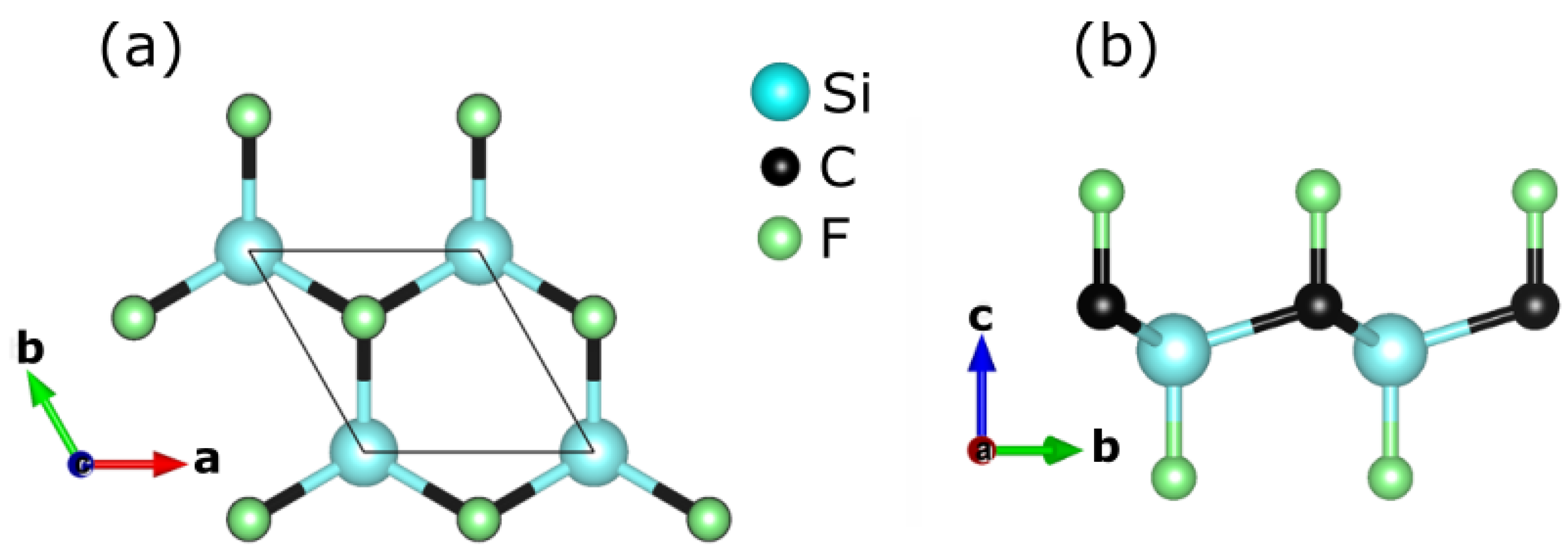
The structure under investigation has a space group P3m1 with a trigonal shape (T1), see Figure 1, which means that the lattice parameters a and b are equal. As a result, the optimized lattice parameter was limited to the a parameter, which was calculated to be 3.16 Å. Unfortunately, no experimental data were available to compare with it. As a result, it was necessary to examine the structure’s stability as well as its growth conditions. In terms of thermodynamic stability, the chemical potentials of the constituent atoms of the CFSi low-dimensional structure obeyed several restrictions based on the energetic equilibrium as follows:
where , , , , , , , and are the chemical potentials for the computing elements, and corresponds to the investigated low-dimensional structure
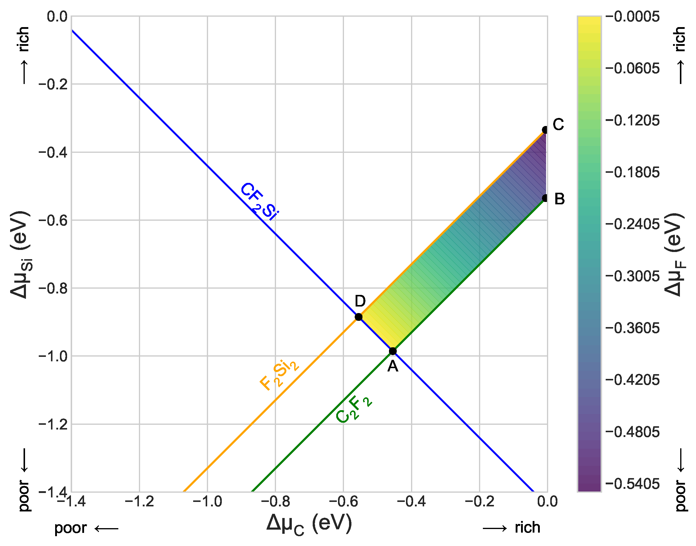
We present the resulting limiting conditions and the intersection points bounding the stability region in Table 1. Figure 2 shows its corresponding diagram. According to this diagram, the title structure competes mainly with the FSi and CF monolayers. We can stipulate this conclusion by taking a number of equations into consideration, considering the constraints to building this structure.
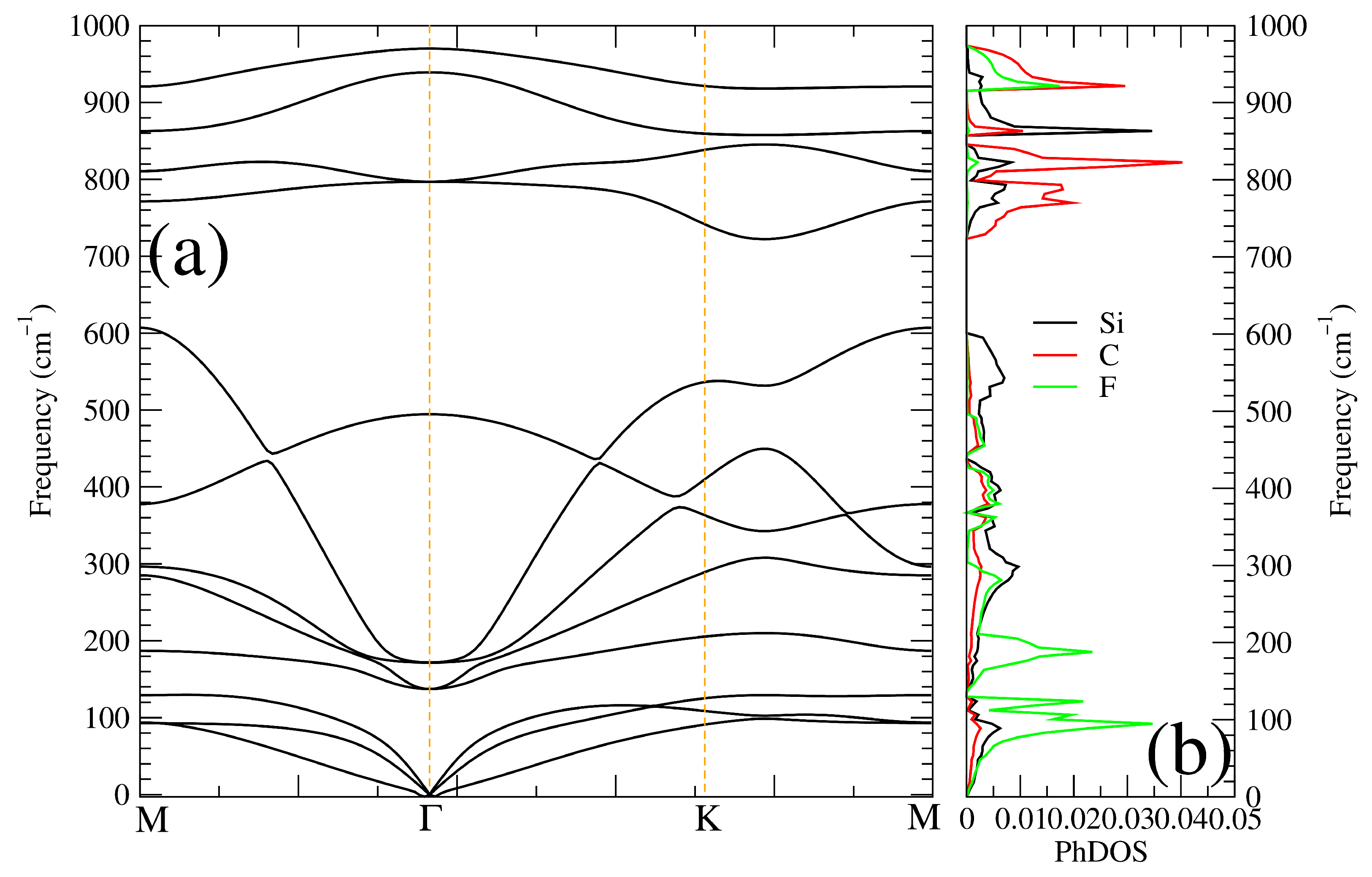
According to all of the above equations and the diagram in Figure 2, the CFSi growth is preferred for intersection points bounding along points A (Si-poor, C-rich, F-rich) where the CFSi competes. We also analyzed the dynamical stability of the low-dimensional structure in the title. This task was done via the calculation of the phonon dispersion spectrum displayed in Figure 3a. Due to the absence of an imaginary frequency, we can clearly see that the structure is mechanically stable. The shape of the plot seems to share the general scheme of 2D chalcogenide structures. We can note some anomalies in the form of longitudinal acoustic branches, the signature of weak interplanar interactions. According to [34], these acoustic modes have a linear dependence in the q-space near the point. The modes at the center of the point, according to the crystal point group, obey the formula , where and . The E mode denotes the double degenerated one. The analysis of the activity of each mode shows that they are both Raman and infrared ones. The calculated wavenumbers for each mode are gathered in Table 2.
At the same time, the phonon density of state gathered in Figure 3 shows that the acoustic branches were mainly formed from the lighter atoms, namely the F one, and the branches at high frequency originated from the carbon one. To assess more information on the mechanical properties of the studied structure, we also evaluated the elastic constants of CFSi. The results are shown in Table 3. The mechanical stability of the 2D CFSi monolayer can be examined by using the elastic constants C. For symmetry reasons, we had only two elastic stiffness components, C and C, the C = (C− C)/2. Because CFSi is bidimensional, the Born criteria of mechanical stability should satisfy the conditions C > 0 and C > 0 [35,36,37]. According to the calculated results of C, the mechanical stability was satisfied, implying that the investigated structure would eventually be mechanically stable in its low-dimensional structure.
According to the results of this table, and due to its buckled nature, the compound was rather rigid and had comparable properties to its SiC counterpart in the 2D honeycomb structure [21]. The application of strain on the 2D-SiC honeycomb structure showed a stable structure until 17% of compression. CFSi in fact manifested comparable dynamical properties as TH-SiC and TH-SiC structures. C (119.7 N/m) and C (26.5 N/m) had values that were close to TH-SiC ((T) and (H) stand, respectively, for tetragonal and hexagonal structures). The main small difference was mainly due to the F atom bonded in the out-plane direction of the Si–C bonds. As a result, the structure was less covalent than a TH-SiC, TH-SiC, or h-SiC monolayer and then more ductile along the shear direction. Furthermore, the shear modulus of CFSi was 17% lower than that of TH-SiC [38]. This allowed a precise application of strain along the shear direction.
3.2. Low-Dimensional CFSi Structure under Shear Tensile Strain
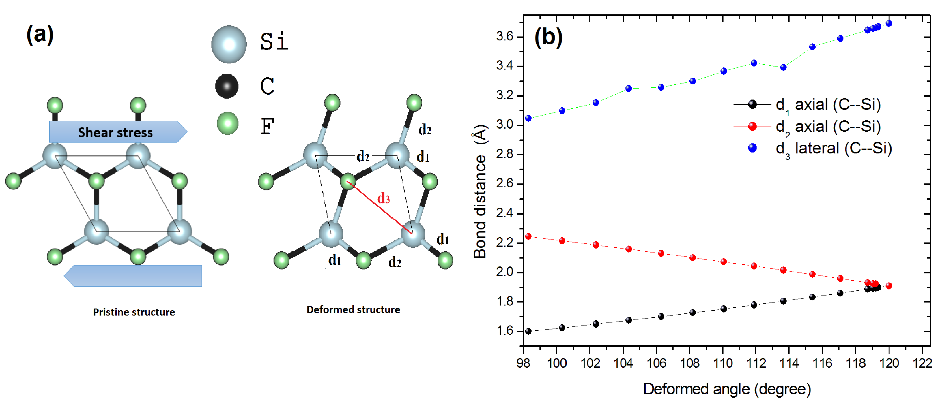
Starting with the fully relaxed 2D crystal structure CFSi, we simulated the shear tensile strain by decreasing the value of the angle from 120 to 98 (see Figure 4a,b). The tensile strain was defined as , where and are the lattice constants of the strained and relaxed structure, respectively. After the application of such a strain, the structure was fully relaxed, keeping the volume and lattice parameters constant, but allowing the relaxation of the internal atomic coordinates. The shear strain was applied step by step until reached a value of 98 of the initial = 120 angle.
To gain a better understanding of the structure’s trend under shear deformation, we plotted the evolution of the C–Si bonds as a function of in three directions in Figure 4b. The linear compressibility of the d and d axial bonds was correlated. They gave a value of GPa, where the lateral direction d had a linear compressibility of GPa. According to this result, we believe that the enlargement of the d C–Si bonds under shear compression was responsible for the increase of most high-frequency modes and was a consequence of the change in the band-gap nature. Qualitatively, under the harmonic approximation, the stretching mode was proportional to frequency [39]. Thus, according to our mode assignment, the strongest Raman active mode related to the carbon atoms, and located at a wavenumber of 970.1 cm, increased to 1354.86 cm under a shear deformation of 18%. This result implied that the structure was rather compressible under shear deformation.
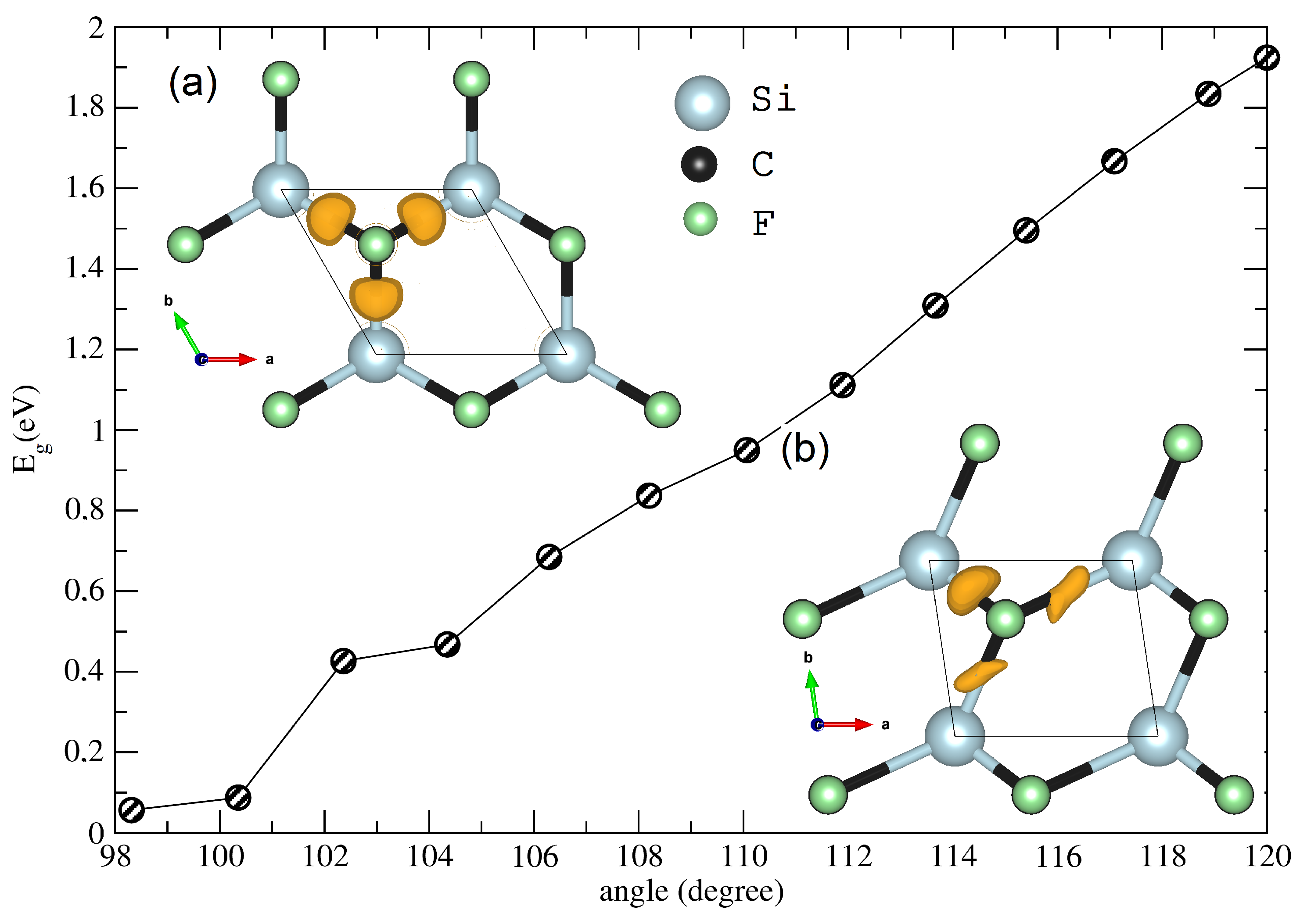
In a subsequent step, we analyzed the effect of an imposed strain on the electronic band gap of the investigated structure. The result is gathered in Figure 5. The calculation of the band gap of the unstrained structure within the Heyd–Scuseria–Ernzerhof hybrid density functional (HSE06) [40] gave a value of 3.31 eV, whereas the PBE gave a band gap of 1.94 eV. The plot shows that with the increase of tensile strain, the band gap decreased and vanished for a strain of 18% on the structure. The new Si–C–Si reached a value of 98, and this behavior (semiconductor-to-metal transition) was also shown in the application of a zigzag strain on the 2D–SiC [21]. As a result, we suspect a corresponding electronic transformation on the CFSi structure.
In order to understand this electronic transformation, we analyzed the nature of both Si–C and C–F bonds for strained and pristine structures. For this task, we performed the electron localization function (ELF) designed by Becke and Edgecombe [24] according to the method proposed by Savin et al. [41]. The ELF topology gives a partition into localized electronic domains known as basins. They are used to rationalize the bonding schemes. The synaptic order of a valence ELF basin is determined by the number of core basins with which they share a common boundary. The basins’ spatial locations are very close to the valence-shell electron-pair repulsion domains [42]. According to Savin et al. [41], in the DFT framework, the ELF can be understood as a local measure of the excess of local kinetic energy of electrons, . This quantity is computed by subtracting the bosonic contribution, , from the kinetic energy density of the system, . A rescaling of it with respect to the homogeneous electrons gas provides the core of the ELF, :
where is the Fermi constant. Accordingly, the regions of electron pairing would have a small value. In order to inverse this relationship and map it in a closed interval, the final function was defined as follows:
The ELF partition shown in the inset of Figure 5 depicts two cases: the top for pristine structure, which depicts three disynaptic basins ELF–V(Si, C) built at isosurface .
These basins had similar shapes and populations (see Table 4), while both basins V(Si,C) and V(C,Si) had and their population was approximately equal to two electrons, indicating their covalent nature. Table 4 also indicates the existence of a monosynaptic basin V(F) with an ionic nature (), plus a small disynaptic V(C, F) basin (), with a weak electronic population. This behavior was a result of the strong polarization between the in-plane Si–C and C–F bonds. While the charge density () in the covalent bonds was weak, the ionic one in V(F) was strong. On the other hand, the strained structure showed deformed electronic basins. In the strained structure, the covalent disynaptic V(C, Si) basins also appeared, as well as new monosynaptic ones, for instance, a V(Si) basin with a small , as well as three polarized ionic V(F) basins, where we could show an increase in the electron population. We could also show an increase in the metallicity of the bonds and an extension of the charge density. The asymmetry in the bond population and the electronic volume of the emerged basins were attributed to the strong distortion of the strained structure.
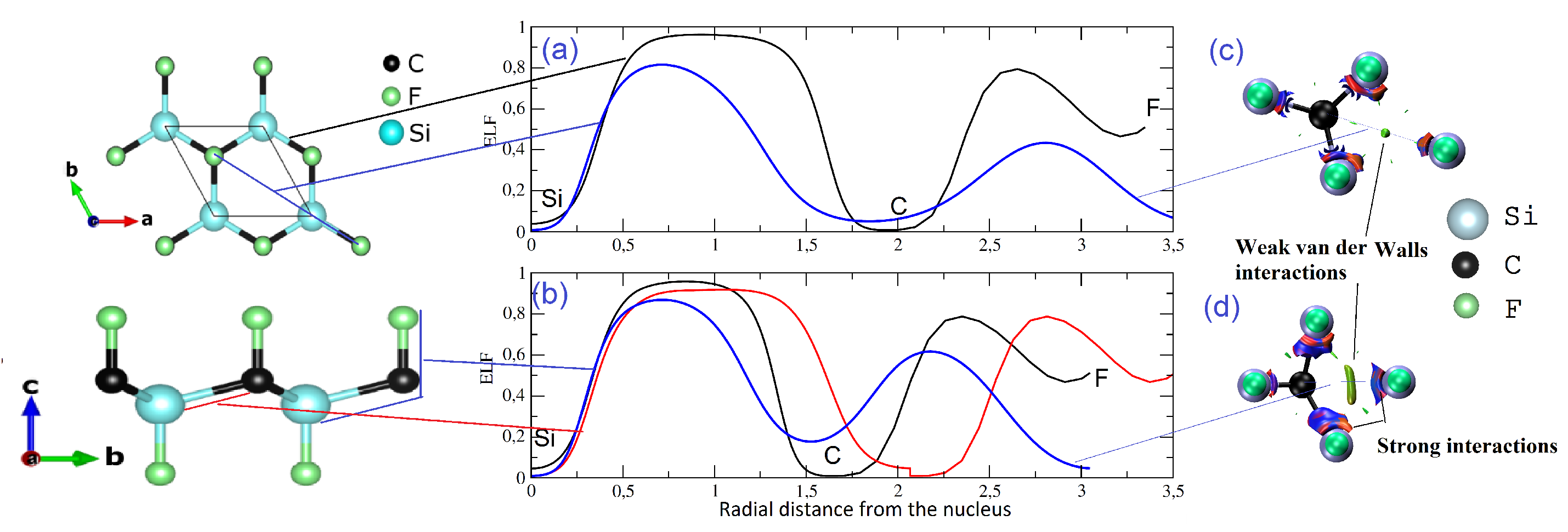
A deeper analysis can untangle this behavior with both the 1D ELF profile and the NCI index. In Figure 6a,b, we displayed the ELF profile of Si–C–F, of unstrained and strained structures in black, the deformed Si–C–F bond of a strained structure in red, and also the lateral direction of Si–C–F of both structures in blue. The 1D ELF profile confirmed that the Si–C bond was covalent and C–F ionic, but it also confirmed the existence of a metallic plateau in the lateral direction of Si–C–F showing a region of very low ELF values with a small hill around . The same trend was noticed whilst studying the bulk SiC under strain [20]. In fact, in the application of tensile strain, the Si–C bond length built from the unit cell of the CFSi structure became different. This distortion enhanced the noncovalent interactions in the nonbonded Si and C direction. Given the relevance of this result, we used the same tool as in [20]. The noncovalent interactions’ (NCI) isosurface is presented in Figure 6c,d. The noncovalent domain seemed to increase from the unstrained to the strained structure in the nonbonded Si–C–F direction. This region, in fact, did not play any meaningful role in the cohesion of low-dimensional CFSi, but rather in the stability and the enhancement of the polarization of bonds. This could be shown in the region of blue surrounding the distorted Si–C bonds of the strained structure, which explained the increase in ionicity and metallicity.
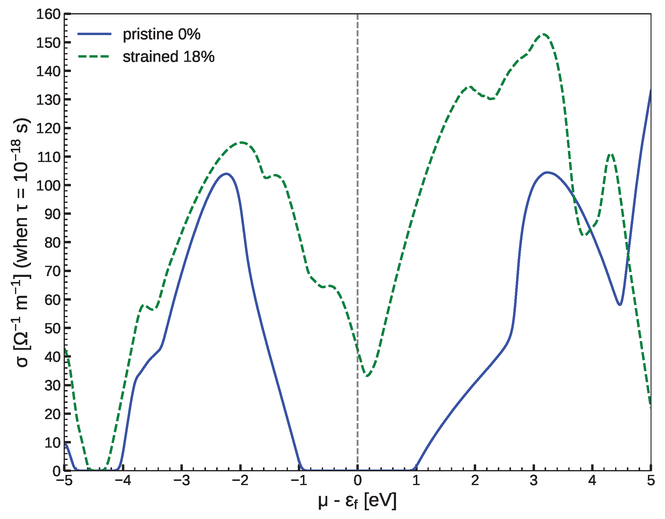
Finally, to investigate the relationship between conductivity and shear effect on the low-dimensional CFSi structure, we used the semiclassical Boltzmann transport theory with a fixed relaxation time approximation to predict the electrical conductivity (). This task was done by the use of the BoltzTraP code [43]. We note that, as the procedure was related to the band structure calculation, we took care to increase the grid of the calculation by the use of k-points. Figure 7 gives the ( being the relaxation time) at 300 K as a function of the carrier concentration for both pristine (0%) and strained (18%) structures. We can see that the tensile shear strain increased in both the p- and n-type doped systems. In fact, the increase in coincided with that of the band gap. Therefore, the electrical conductivity was efficiently tuned by the strain via band structure engineering. It was noted that the p-type doped region was more affected due to the closing of the band gap.
4. Summary
We showed in this contribution that when the CFSi low-dimensional structure was submitted to the application of tensile strain along the shear direction, an electronic transition occurred from the semiconducting phase with a wide electronic band gap to a metallic one with a vanishing band gap. A first attempt to understand this transformation was made within the density functional method calculation, by calculating the stability and mechanical properties of the investigated structure. Furthermore, to understand this mechanism, we used the inherent topological bonding. This task allowed us to understand that this transition was a response to the new repartition of the electronic population and an enhancement of weak noncovalent interactions along the nonbonded directions of the unit cell. Overall, such interactions could be responsible for the relative stability of the structure and also play an important role in controlling the nature of the electronic wave function describing the computed structure. The increase of electric conductivity as a function of strain stipulated the poor performance of the CFSi low-dimensional structure as a thermoelectric system.
Author Contributions
Conceptualization, methodology, validation, formal analysis, investigation, writing—original draft preparation, writing—review and editing, supervision, T.O.; DFT calculation, review and editing, R.M.B. All authors have read and agreed to the published version of the manuscript.
Funding
This research received no external funding.
Institutional Review Board Statement
Not applicable.
Informed Consent Statement
Not applicable.
Data Availability Statement
Data are available upon request from the corresponding author.
Acknowledgments
T.O. acknowledges the financial support given by the PRFU, no. B00L02EP13022-0230001.
Conflicts of Interest
The authors declare no conflict of interest.
References
- Barreteau, C.; Michon, B.; Besnard, C.; Giannini, E. High-pressure melt growth and transport properties of SiP, SiAs, GeP, and GeAs 2D layered semiconductors. J. Cryst. Growth 2016, 443, 75–80. [Google Scholar] [CrossRef] [Green Version]
- Schaack, S.; Depondt, P.; Huppert, S.; Finocc, H.F. Quantum driven proton diffusion in brucite-like minerals under high pressure. Sci. Rep. 2020, 10, 8123. [Google Scholar] [CrossRef] [PubMed]
- Li, W.; Qian, X.; Li, J. Phase transitions in 2D materials. Nat. Rev. Mater. 2021, 6, 829–846. [Google Scholar] [CrossRef]
- Voiry, D.; Yamaguchi, H.; Li, J.; Silva, R.; Alves, D.C.B.; Fujita, T.; Chen, M.; Asefa, T.; Shenoy, V.B.; Eda, G.; et al. Enhanced catalytic activity in strained chemically exfoliated WS2 nanosheets for hydrogen evolution. Nat. Mater. 2013, 12, 850–855. [Google Scholar] [CrossRef] [PubMed]
- Eda, G.; Fujita, T.; Yamaguchi, H.; Voiry, D.; Chen, M.; Chhowalla, M. Coherent atomic and electronic heterostructures of single-layer MoS2. ACS Nano 2012, 6, 7311–7317. [Google Scholar] [CrossRef]
- Cai, X.; Ren, Y.; Wu, M.; Xu, D.; Luo, X. Strain-induced phase transition and giant piezoelectricity in monolayer tellurene. Nanoscale 2020, 12, 167. [Google Scholar] [CrossRef]
- Nayak, A.P.; Bhattacharyya, S.; Zhu, J.; Liu, J.; Wu, X.; Pandey, T.N.; Jin, C.; Singh, A.K.; Akinwande, D.; Lin, J.-F. Pressure-induced semiconducting to metallic transition in multilayered molybdenum disulphide. Nat. Commun. 2014, 5, 3731. [Google Scholar] [CrossRef] [Green Version]
- Fleurence, A.; Friedlein, R.; Ozaki, T.; Kawai, H.; Wang, Y.; Yamada-Takamura, Y. Experimental evidence for epitaxial silicene on diboride thin films. Phys. Rev. Lett. 2012, 108, 245501. [Google Scholar] [CrossRef]
- Li, Y.; Li, F.; Zhou, Z.; Chen, Z. SiC2 silagraphene and its one-dimensional derivatives: Where planar tetracoordinate silicon happens. J. Am. Chem. Soc. 2011, 133, 900–908. [Google Scholar] [CrossRef]
- Zhou, L.J.; Zhang, Y.F.; Wu, L.M. SiC2 siligraphene and nanotubes: Novel donor materials in excitonic solar cells. Nano Lett. 2013, 13, 5431–5436. [Google Scholar] [CrossRef]
- Ding, Y.; Wang, Y. Geometric and electronic structures of two-dimensional SiC3 compound. J. Phys. Chem. C. 2014, 118, 4509–4515. [Google Scholar] [CrossRef]
- Borlido, P.; Huran, A.W.; Marques, M.A.L.; Botti, S. Novel two-dimensional silicon-carbon binaries by crystal structure prediction. Phys. Chem. Chem. Phys. 2020, 22, 8442–8449. [Google Scholar] [CrossRef] [PubMed]
- Fan, D.; Lu, S.; Guo, Y.; Hu, X. Novel bonding patterns and optoelectronic properties of the two-dimensional SixCy monolayers. J. Mater. Chem. C. 2017, 5, 3561–3567. [Google Scholar] [CrossRef] [Green Version]
- Xu, Y.; Ning, Z.; Zhang, H.; Ni, G.; Shao, H.; Peng, B.; Zhang, X.; He, X. Anisotropic ultrahigh hole mobility in two-dimensional penta-SiC2 by strain-engineering: Electronic structure and chemical bonding analysis. RSC Adv. 2017, 7, 45705–45713. [Google Scholar] [CrossRef] [Green Version]
- Kilic, M.E.; Lee, K.-R. Tetrahex Carbides: Two-Dimensional Group-IV Materials for Nanoelectronics and Photocatalytic Water Splitting. Carbon 2021, 174, 15. [Google Scholar] [CrossRef]
- Feng, W.; Long, P.; Feng, Y.; Li, Y. Two-Dimensional Fluorinated Graphene: Synthesis, Structures, Properties and Applications. Adv. Sci. 2016, 3, 1500413. [Google Scholar] [CrossRef]
- Glass, C.W.; Oganov, A.R.; Hansen, N. USPEX—Evolutionary crystal structure prediction. Comput. Phys. Commun. 2006, 175, 713. [Google Scholar] [CrossRef]
- Martonak, R.; Laio, A.; Bernasconi, M.; Ceriani, C.; Raiteri, P.; Parrinello, M. Simulation of structural phase transitions by metadynamics. Z. Krist. 2005, 220, 489. [Google Scholar]
- Ouahrani, T.; Merad-Boudia, I.; Baltache, H.; Khenata, R.; Bentalha, Z. Effect of pressure on the global and local properties of cubic perovskite crystals. Phys. Scr. 2011, 84, 025704. [Google Scholar] [CrossRef] [Green Version]
- Guedda, H.Z.; Ouahrani, T.; Morales-García, A.; Franco, R.; Salvado, M.A.; Pertierra, P.; Recio, J.M. Computer simulations of 3C-SiC under hydrostatic and non-hydrostatic stresses. Chem. Phys. Chem. Phys. 2016, 18, 8132–8139. [Google Scholar] [CrossRef]
- Belarouci, S.; Ouahrani, T.; Benabdallah, N.; Morales-García, A.; Belabbas, I. Two-dimensional silicon carbide structure under uniaxial strains, electronic and bonding analysis. Comp. Mater. Sci. 2018, 151, 288–295. [Google Scholar] [CrossRef]
- Bohorquez, H.; Boyd, R.J. A localized electrons detector for atomic and molecular systems. Theor. Chem. Acc. 2010, 127, 393. [Google Scholar] [CrossRef]
- Bohorquez, H.J.; Matta, C.F.; Boyd, R.J. The localized electrons detector as an ab initio representation of molecular structures. Int. J. Quantum Chem. 2010, 110, 2418. [Google Scholar] [CrossRef]
- Becke, A.D.; Edgecombe, K.E. A simple measure of electron localization in atomic and molecular systems. J. Chem. Phys. 1990, 92, 5397–5404. [Google Scholar] [CrossRef]
- Kresse, G.; Furthmüller, J. Efficiency of ab initio total energy calculations for metals and semiconductors using a plane-wave basis set. Comput. Mat. Sci. 1996, 6, 15–50. [Google Scholar] [CrossRef]
- Kresse, G.; Hafner, J. Ab initio molecular dynamics for liquid metals. Phys. Rev. B 1993, 47, 558–561. [Google Scholar] [CrossRef]
- Kresse, G.; Joubert, D. From ultrasoft pseudopotentials to the projector augmented-wave method. Phys. Rev. B 1999, 59, 1758–1775. [Google Scholar] [CrossRef]
- Perdew, J.P.; Burke, K.; Ernzerhof, M. Generalized Gradient Approximation Made Simple. Phys. Rev. Lett. 1996, 77, 3865–3868. [Google Scholar] [CrossRef] [Green Version]
- Grimme, S.; Antony, J.; Ehrlich, S.; Krieg, S. A consistent and accurate ab initio parametrization of density functional dispersion correction (DFT-D) for the 94 elements H-Pu. J. Chem. Phys. 2010, 132, 154104. [Google Scholar] [CrossRef] [Green Version]
- Grimme, S.; Ehrlich, S.; Goerigk, L. Effect of the damping function in dispersion corrected density functional theory. J. Comp. Chem. 2011, 32, 1456–1465. [Google Scholar] [CrossRef]
- Wang, V.; Xu, N.; Liu, J.C.; Tang, G.; Geng, W.T. VASPKIT: A User-Friendly Interface Facilitating High-Throughput Computing and Analysis Using VASP Code. Comput. Phys. Commun. 2021, 267, 108033. [Google Scholar] [CrossRef]
- Togo, A.; Tanaka, I. First principles phonon calculations in materials science. Scr. Mater. 2015, 108, 1–5. [Google Scholar] [CrossRef] [Green Version]
- Kozlowski, D.; Pilmé, J. New Insights in Quantum Chemical Topology Studies Using Numerical Grid-based Analyses. J. Comput. Chem. 2011, 32, 3207. [Google Scholar] [CrossRef] [PubMed]
- Ougherb, C.; Ouahrani, T.; Badawi, M.; Morales-García, A. Effect of the sulfur termination on the properties of Hf2CO2 MXene. Phys. Chem. Chem. Phys. 2022, 24, 7243–7252. [Google Scholar] [CrossRef] [PubMed]
- Born, M.; Huang, H. Dynamical Theory of Crystal Lattices; Oxford University Press: Clarendon, UK, 1954; 432p, ISBN 9780198503699. [Google Scholar]
- Mouhat, F.; Coudert, F.X. Necessary and sufficient elastic stability conditions in various crystal systems. Phys. Rev. B. 2014, 90, 224104. [Google Scholar] [CrossRef] [Green Version]
- Sekkal, A.; Benzair, A.; Ouahrani, T.; Faraoun, H.I.; Merad, G.; Aourag, H. Mechanical properties and bonding feature of the YAg, CeAg, HoCu, LaAg, LaZn, and LaMg rare-earth intermetallic compounds: An ab initio study. Intermetallics 2014, 45, 65–70. [Google Scholar] [CrossRef]
- Wei, Q.; Yang, Y.; Yang, G.; Peng, V. New stable two dimensional silicon carbide nanosheets. J. Alloys Compd. 2021, 868, 159201. [Google Scholar] [CrossRef]
- Chen, G.; Haire, R.G.; Peterson, J.R. Compressibilities of TbVO4 and DyVO4 Calculated from Spectroscopic Data. Appl. Spectrosc. 1992, 46, 1495–1497. [Google Scholar] [CrossRef]
- Heyd, J.; Scuseria, G.E.; Ernzerhof, M. Hybrid functionals based on a screened Coulomb potential. J. Chem. Phys. 2003, 118, 8207–8215. [Google Scholar] [CrossRef] [Green Version]
- Savin, A.; Jepsen, O.; Flad, J.; Anderson, L.K.; Preuss, H.; von Schnering, H.G. Electron localization in solid-state structures of the elements: The diamond structure. Angew. Chem. Int. Ed. Engl. 1992, 32, 187–188. [Google Scholar] [CrossRef]
- Gillespie, R.J.; Nyholm, R.S. Inorganic stereochemistry. Quart. Rev. 1957, 11, 339–380. [Google Scholar] [CrossRef]
- Madsen, G.K.H.; Singh, D.J. BoltzTraP. A code for calculating band-structure dependent quantities. Comput. Phys. Commun. 2006, 175, 67–71. [Google Scholar] [CrossRef]
Figure 1.
(a) The top and (b) the side views of CFSi in its low-dimensional structure.

Figure 2.
Chemical potential’s phase diagram, showing the region of stability of CFSi in terms of the excess chemical potentials. (Color online) Variation in formation enthalpy as a function of chemical potential, shown within the stability region for the formation of low dimensional CFSi. Points A, B, C, and D are shown only in order to delimit the zone of stability.

Figure 3.
(a) Phonon dispersion plot and its corresponding (b) phonon density of states of CFSi monolayer in cm.
Figure 3.
(a) Phonon dispersion plot and its corresponding (b) phonon density of states of CFSi monolayer in cm.

Figure 4.
(a) Schematic representation of the pristine and strained (deformed) structure of CFSi monolayer. (b) Calculated strain dependence of C–Si bond distances. d, d represent the axial bonds and d the lateral bonds.
Figure 4.
(a) Schematic representation of the pristine and strained (deformed) structure of CFSi monolayer. (b) Calculated strain dependence of C–Si bond distances. d, d represent the axial bonds and d the lateral bonds.

Figure 5.
Evolution of the band gap as a function of gamma angle. The inset shows the 3D-ELF isosurface of the structure at (a) (unstrained) 0% and (b) (strained) 18% of the tensile strain.
Figure 5.
Evolution of the band gap as a function of gamma angle. The inset shows the 3D-ELF isosurface of the structure at (a) (unstrained) 0% and (b) (strained) 18% of the tensile strain.

Figure 6.
Left, one-dimensional ELF profile of bonds for (a) pristine and (b) strained CFSi monolayer. The black, blue, and red correspond, respectively, to Si–C–F, deformed Si–C–Si for strained structure, and Si–C–F lateral direction. Right, the noncovalent interactions index NCI = 0.3 isosurface of (c) pristine and (d) strained structures.

Figure 7.
Calculated electrical conductivity of pristine (0%) and strained (18%) structures at ambient temperature. The electrical conductivity was calculated with respect to the relaxation time . The transporting directions are not distinguished here.
Figure 7.
Calculated electrical conductivity of pristine (0%) and strained (18%) structures at ambient temperature. The electrical conductivity was calculated with respect to the relaxation time . The transporting directions are not distinguished here.


Table 1.
The limiting inequalities applied to the independent variables and . The point column lists the intersection points bonding the stability region. The corresponding values of the dependent variable and the relevant competing phases are also given. All energies are in eV.
Table 1.
The limiting inequalities applied to the independent variables and . The point column lists the intersection points bonding the stability region. The corresponding values of the dependent variable and the relevant competing phases are also given. All energies are in eV.
| Limiting Inequalities | Point | Competing Phases |
|---|---|---|
| A(−0.4550, −0.9855, 0.0000) | CFSi, CF | |
| B(−0.0050, −0.5355, −0.4500) | CF | |
| C(−0.0050, −0.3345, −0.5505) | FSi | |
| D(−0.5555, −0.8850, 0.0000) | CFSi, FSi | |
Table 2.
Calculated modes of 2D CFSi. Raman (R) and infrared (IR) modes are indicated.
| Symmetry | (cm) | Activity |
|---|---|---|
| A | 494.5 | IR/R |
| A | 939.2 | IR/R |
| A | 970.0 | IR/R |
| E | 137.2 | IR/R |
| E | 171.7 | IR/R |
| E | 797.0 | IR/R |
Table 3.
Calculated lattice parameters, elastic components, and elastic modulus of CFSi monolayer.
| a (Å) | C (N/m) | C (N/m) | E (N/m) | G (N/m) | K (N/m) | |
|---|---|---|---|---|---|---|
| 3.16086 | 118.543 | 22.410 | 114.306 | 48.067 | 70.477 | 0.189 |
Table 4.
Electron localization analysis of a basin of bonding of the CFSi monolayer. V(), q, bond metallicity (), and stand, respectively, for basin volumes of disynaptic V(X,Y) and monosynaptic V(X) bonds, electronic charges of the bond, calculated bond metallicity and electronic density charge (), and ELF () basin.
| Basin | V() (Bohr) | q (Electrons) | ELF | Bond Metallicity () | (Atomic Units) |
|---|---|---|---|---|---|
| pristine | |||||
| V(C,Si) | 67.784 | −2.1654 | 0.9617 | −0.4906 | 0.12872651 |
| V(Si,C) | 71.167 | −2.2023 | 0.9617 | −0.4906 | 0.12872651 |
| V(F) | 57.249 | −2.4110 | 0.7945 | −1.2574 | 2.07097897 |
| V(F,C) | 3.137 | −0.7520 | 0.8466 | 0.2796 | 0.37723410 |
| strained | |||||
| V(C,Si) | 19.022 | −1.9622 | 0.9608 | −0.3428 | 0.23750961 |
| V(C,Si) | 35.711 | −0.6928 | 0.9252 | −0.5682 | 0.07178674 |
| V(Si,C) | 33.542 | −1.4756 | 0.9236 | −0.5340 | 0.09279469 |
| V(C,Si) | 33.642 | −1.4252 | 0.9175 | −2.4263 | 0.10376149 |
| V(Si) | 52.592 | −2.2627 | 0.4977 | −0.3529 | 2.07237211 |
| V(F) | 73.435 | −3.3421 | 0.8837 | −0.5505 | 0.06132580 |
| V(F) | 42.653 | −3.3972 | 0.8746 | −0.5486 | 0.05989116 |
| V(F) | 48.171 | −1.9589 | 0.8696 | 0.2769 | 0.37582815 |
| V(F,C) | 3.124 | −0.7088 | 0.8478 | 0.2791 | 0.37814979 |
Publisher’s Note: MDPI stays neutral with regard to jurisdictional claims in published maps and institutional affiliations. |
© 2022 by the authors. Licensee MDPI, Basel, Switzerland. This article is an open access article distributed under the terms and conditions of the Creative Commons Attribution (CC BY) license (https://creativecommons.org/licenses/by/4.0/).
Share and Cite
MDPI and ACS Style
Ouahrani, T.; Boufatah, R.M. Understanding the Semiconducting-to-Metallic Transition in the CF2Si Monolayer under Shear Tensile Strain. Crystals 2022, 12, 1476. https://0-doi-org.brum.beds.ac.uk/10.3390/cryst12101476
AMA Style
Ouahrani T, Boufatah RM. Understanding the Semiconducting-to-Metallic Transition in the CF2Si Monolayer under Shear Tensile Strain. Crystals. 2022; 12(10):1476. https://0-doi-org.brum.beds.ac.uk/10.3390/cryst12101476
Chicago/Turabian StyleOuahrani, Tarik, and Reda M. Boufatah. 2022. "Understanding the Semiconducting-to-Metallic Transition in the CF2Si Monolayer under Shear Tensile Strain" Crystals 12, no. 10: 1476. https://0-doi-org.brum.beds.ac.uk/10.3390/cryst12101476
Note that from the first issue of 2016, this journal uses article numbers instead of page numbers. See further details here.