
Many-Body Calculations of Excitons in Two-Dimensional GaN

Guizhou Provincial Key Laboratory of Computational Nano-Material Science, Guizhou Education University, Guiyang 550018, China
Crystals 2023, 13(7), 1048; https://0-doi-org.brum.beds.ac.uk/10.3390/cryst13071048
Submission received: 4 June 2023
/
Revised: 25 June 2023
/
Accepted: 30 June 2023
/
Published: 1 July 2023
(This article belongs to the Special Issue In Celebration of the 30th Anniversary of Shuji Nakamura’s Contribution to Blue Light-emitting Diodes)
Abstract
:We present an ab initio study on quasiparticle (QP) excitations and excitonic effects in two-dimensional (2D) GaN based on density-functional theory and many-body perturbation theory. We calculate the QP band structure using approximation, which generates an indirect band gap of eV () for 2D GaN, opening up eV with respect to its bulk counterpart. It is shown that the success of plasmon-pole approximation in treating the 2D material benefits considerably from error cancellation. On the other hand, much better gaps, comparable to ones, could be obtained by correcting the Kohn–Sham gap with a derivative discontinuity of the exchange–correlation functional at much lower computational cost. To evaluate excitonic effects, we solve the Bethe–Salpeter equation (BSE) starting from Kohn–Sham eigenvalues with a scissors operator to open the single-particle gap. This approach yields an exciton binding energy of eV in 2D GaN, which is in good agreement with the highly demanding -BSE results. The enhanced excitonic effects due to reduced dimensionality are discussed by comparing the optical spectra from BSE calculations with that by random-phase approximation (RPA) for both the monolayer and bulk GaN in wurtzite phase. Additionally, we find that the spin–orbit splitting of excitonic peaks is noticeable in 2D GaN but buried in the bulk crystal.
1. Introduction
The group III nitrides cover a wide range of band gaps (– eV) [1,2]. These semiconductors are of great interest for the fabrication of optoelectronic devices [3], which may enable us to access light emission over a broad-spectrum region from infrared to ultraviolet [4,5]. Among them, GaN has been by far the most widely explored material in solid-state lighting applications [6]. The most stable wurtzite-phase GaN is a direct band gap ( = eV) semiconductor, and the wide gap allows a high breakdown field that is critical in developing high-power electronic devices [7,8]. Despite extensive theoretical and experimental studies devoted to bulk GaN [9,10,11,12], relatively little is known about the atomically thin two-dimensional (2D) GaN [13].
The quantum confinement in 2D GaN considerably increases the band gap and represents a promising way to push the emission into the deep ultraviolet regime [14]. A recent study has shown that the electronic structure and magnetic properties of 2D GaN could be effectively tuned by doping with elements from groups III–VI [15]. More importantly, the monolayer semiconductor offers a good opportunity for stacking into van der Waals heterostructures (vdWHs) [16] that are flexible and hold great promise for ultra-thin nanodevice applications. Many of them, e.g., solar cells [17,18] and photodetectors [19,20,21], entail an efficient dissociation of the tightly bound electron–hole pairs (excitons) into free carriers. Unfortunately, due to reduced dimensionality, the Coulomb attractions between electrons and holes are normally enhanced as a result of weakened dielectric screening in typical 2D materials [22,23]. These effects highlight the need for a systematic study on excitons in 2D GaN, which would be essential for a rational design of device materials. An effective way to tackle excitonic effects in semiconductors is the Bethe–Salpeter equation (BSE) [24,25,26], which enables us to obtain optical absorption spectra well in agreement with experiment. The exciton binding energy can be evaluated from the difference between the direct band gap and the lowest excitonic level given by BSE as illustrated in Figure 1.
However, it has been established that both local and semi-local exchange–correlation (xc) functionals tend to underestimate band gaps of solids in density-functional theory (DFT) calculations [27]. In fact, the single-particle approximation within DFT fails to capture quasiparticle (QP) energies (the energy change upon removing or injecting an electron) even with exact xc functionals [28,29]. This issue has been demonstrated to be more severe in 2D materials due to reduced screening [30,31]. To overcome this problem, one needs to go beyond the mean-field picture and consider effectively the many-body effects for the description of QP excitations in 2D materials [32,33,34]. Though a number of studies have explored the excitonic effects in 2D GaN [35,36,37,38], these calculations rely heavily on the -BSE combination which is computationally demanding and probably unaffordable for extended materials such as vdWHs [39,40]. More recently, several frameworks have been developed toward reducing the cost by replacing the many-body approximation with Koopmans-compliant (KC) functionals [41] or localized orbital scaling correction (LOSC) [42]. Despite encouraging results, further simplification is still favorable for realistic materials simulations. Furthermore, previous studies on 2D GaN neglect the effect of spin–orbit coupling (SOC). While the SOC effect is small in bulk GaN [43], it plays a key role in quantum well structure [44] and radiative lifetimes [45]. It is still unclear whether this effect can be neglected when exploring the optical properties of 2D GaN. Therefore, further work is needed to address these issues.
In this work, we perform a detailed analysis on the electronic and excitonic properties of GaN, focusing on the difference between freestanding 2D GaN and bulk GaN in wurtzite phase. The excitonic effects are studied by solving the BSE on the basis of Kohn–Sham eigenstates and eigenvalues corrected with a scissors operator, which requires much lower computational cost compared to the state-of-the-art -BSE approach. We show that both the optical spectra and lowest exciton binding energy could be well reproduced. We have specified the influence of low dimensionality on quasiparticle excitations and excitonic effects, emphasizing the interplay of strict quantum confinement and reduced dielectric screening. In particular, we demonstrate through a simplified two-band model that the spin–orbit coupling generates a sizable splitting of excitonic peaks in the 2D GaN. These studies could provide a better understanding on the evolution of optical response properties in condensed materials upon transition from bulk to low-dimensional form, and might as well push forward experimental investigations on 2D GaN.
2. Computational Details
All calculations were carried out using the Gpaw package [46], which is implemented based on the projector augmented-wave (PAW) [47] electronic structure method. Plane waves basis sets were used to expand the valence electron wave functions with an energy cutoff of 600 eV. We adopted the residual minimization method—direct inversion in iterative subspace (RMM-DIIS)—as an eigensolver. Both local-density approximation (LDA) under Perdew–Wang (PW92) [48] parameterization and generalized gradient approximation (GGA) of Perdew–Burke–Ernzerhof (PBE) [49] type were employed as exchange–correlation (xc) functionals. In optimizing the lattice constant, a shifted (-centered) k-grid of was employed for Brillouin-zone sampling in wurtzite GaN, and k-points mesh was used for the 2D material.
The single-particle excitation energies can be evaluated by solving the QP equation based on the Green function theory [50],
where specifies the “external” potential due to nuclei, is the Hartree potential, and is the self-energy operator. This non-local, energy-dependent operator accounts for the many-body effects. A working way to calculate is offered by the approximation [50,51], which evaluates by means of a product in spacetime representation within many-body perturbation theory,
where G and W are, respectively, the dressed one-particle Green function and the screened Coulomb interaction.
In realistic materials calculations, the most widely used scheme is the one-shot formalism [52,53,54], in which both G and W are calculated in a straightforward way from Kohn–Sham states without further update. These single-particle states were produced in this study by LDA under denser k-points: for the bulk structure and for the monolayer. An analytic correction to the q = 0 contribution was applied to the 2D material. The plane wave cutoff energy for calculating the self-energy was set to 150 eV, and an extrapolation of the self-energy to infinite was carried out using points at 129, 139, and 150 eV. The number of bands included in the calculations was close to the number of plane waves that were determined from . In calculating the screened Coulomb potential in the GaN monolayer, we used a “2D” truncation scheme to avoid adding a large-size vacuum layer in the perpendicular direction [32,53]. The parameters controlling the frequency grid were specified by = and = .
The eigenvalues of excitons were calculated by diagonalizing the two-particle Hamiltonian [55] derived from the BSE [56],
where represents exciton weights. The Hamiltonian was represented on a transition space including the last four valence bands (VB) and first four conduction bands (CB),
where f refers to the occupation factor and the kernel K is defined by
Here, V and W are the exchange (unscreened) and direct (screened) electron–hole interactions, respectively. When the direct interaction W is neglected, Equation (5) reduces to the random-phase approximation (RPA). The Hamiltonian becomes hermitian under Tamm–Dancoff approximation (only accounting for VB to CB transitions).
The transition space and the resulting were constructed from LDA eigenvalues and eigenstates, and an ad hoc scissors operator was introduced to correct the single-particle levels [57]. Here, was determined by adjusting the Kohn–Sham gap to the QP one produced by . A plane wave cutoff energy of 200 eV was applied for these calculations. In calculating the screened interactions W, 100 bands were included, which were obtained by full diagonalization of the Kohn–Sham Hamiltonian. For comparison, the BSE spectrum was also calculated in a minimal transition space consisting of the highest valence band and lowest conduction band with and without spin–orbit coupling, which was taken into account in a non self-consistent way [58]. Due to the Coulomb truncation in 2D materials, the dimensionless absorbance (ABS) was calculated in optical limit () [24] on the basis of 2D polarizability (in atomic units) through
where represents the energy transfer in the excitation and c is the speed of light.
3. Results and Discussion
3.1. Atomic Structures
We calculate the equilibrium lattice constants of both the bulk GaN in wurtzite-phase and the freestanding 2D material (shown in Figure 2) through a minimization of the electronic energy E with respect to cell volume V. The E–V relationship is obtained according to the stabilized jellium equation of state (SJEOS) [59], which is a third-order inverse polynomial fit as displayed in Figure 3. In building the wurtzite structure, we use an ideal ratio . The internal parameter u is estimated by as implemented by default in the atomic simulation environment (ASE) [60], which is a python package needed to control materials simulation workflows in this study. The model of 2D GaN is set up on the basis of a graphene-like honeycomb monolayer with a 20 Å vacuum between neighboring layers. Both structures are hexagonal and can be characterized here by a single lattice constant a.
By performing a series of convergence tests regarding k-points sampling, we found that a is converged to within Å using a k-grid (in-plane k-mesh of ) for the bulk (2D) GaN. The results predicted by both LDA and PBE are presented in Table 1. For the wurtzite GaN where an X-ray crystal structure [61] is available, it is worthwhile to compare the results provided by different methods. We note that PBE overestimates the lattice constant by about 2%, while LDA could almost precisely reproduce the experimental value (see Figure 3). These results are consistent with previous DFT studies [62].
In the case of 2D GaN, the optimized a is shown to be a bit larger (by –%) than its bulk counterpart. The expansion of crystal lattice can be understood from their slightly different packing styles within each atomic layer, as shown in Figure 2. In the 2D material, the N atoms reside within the plane of Ga atoms. In contrast, both Ga and N atoms are tetrahedrally coordinated in bulk GaN, where the N atoms tend to leave the Ga layers for better coordination to Ga atoms from other layers. Due to the strong interactions between atomic layers, it would be a bit difficult to prepare the monolayer directly via the micromechanical cleavage approach from bulk samples. A promising way to fabricate 2D GaN has been provided by the technique of migration-enhanced encapsulated growth based on epitaxial graphene [13]. Another method of 2D GaN growth has been realized by using the low-temperature droplet epitaxy technique on the Si(111) surface [63].
Additionally, it is interesting to note that our LDA result is in close agreement with the literature value obtained via structural relaxations using the GGA+d method (including orbitals) [64]. Based on these findings, we chose LDA lattice parameters for the following calculations involving electronic excitations and excitonic effects.

Table 1.
Optimized lattice constant a (in Å) of both the bulk wurtzite structure and the monolayer 2D GaN by different exchange–correlation functionals. The results from another work and experiment are also shown for comparison.
Table 1.
Optimized lattice constant a (in Å) of both the bulk wurtzite structure and the monolayer 2D GaN by different exchange–correlation functionals. The results from another work and experiment are also shown for comparison.
| Material | LDA | PBE | Other Work | Expt. |
|---|---|---|---|---|
| Wurtzite GaN 1 | 3.195 | 3.254 | 3.196/3.252 (LDA/PBE) [62] | 3.190 [61] |
| 2D GaN | 3.218 | 3.272 | 3.21 (PBE) [64] | – |
1 ratio is fixed at , and the internal parameter u is set to by default.
3.2. Quasiparticle Bandstructures
We begin to explore the electronic excitations in GaN by calculating both the Kohn–Sham gap and the quasiparticle band gap. It is shown that the Kohn–Sham gap converges very fast with respect to the k-mesh. The LDA gap is converged to eV in bulk GaN at the k-grid, and to eV in 2D GaN with a k-points mesh of . In comparison, the quasiparticle gap by G0W0 based on LDA (denoted G0W0@LDA) converges somewhat slower, particularly in the 2D material (see Figure 4). The G0W0@LDA results are converged to within eV when reaching k-points grid for the wurtzite GaN. The QP gap is predicted to be eV under the extrapolation scheme of the plane wave (PW) cutoff energy [54]. In 2D GaN, however, a larger density of k-points () is needed to obtain converged results ( eV). The difficulty in convergence for 2D GaN arises mainly from the strong q dependence of the 2D dielectric function near q = 0 [32,65,66]. Thus, one needs a much more elaborate k-points sampling for 2D materials than that required for bulk solids. It is important to point out that another factor usually causing convergence issues is the artificial long-range interactions in supercell calculations. To circumvent this problem, we use a truncated Coulomb potential along the nonperiodic direction (c axis) [53] for the 2D GaN.
In addition, we see that the PW extrapolation is likely to increase the resulting QP gaps in both materials. The plasmon-pole approximation (PPA) [52] seems to underestimate the gap compared to results under full frequency integration in the bulk material (Figure 4a), while it tends to overestimate it in the 2D case (Figure 4b). It may be noted that due to error cancellation between the lack of full frequency integration and the cutoff of PW expansions, PPA could produce fairly accurate QP gaps that are in excellent agreement with results by PW extrapolation in the 2D GaN (Figure 4b). This may partially justify the use of PPA in calculations for 2D materials, which can reduce the computational cost to a certain degree.
The converged band gaps provided by different methods are summarized in Table 2. First, it shows that LDA and PBE result in almost identical band gaps, and not surprisingly, they severely underestimate the measured gaps in both bulk and 2D GaN, as already revealed by other works [62,67]. While the gaps appear to be slightly larger than previous theoretical results [38,68] due to the PW extrapolation, our results lie within the range of experimental band gaps for both materials [14,69,70]. Interestingly, we find that the improvement over Kohn–Sham gaps could be largely reproduced by including the derivative discontinuity of the xc functional , which has been implemented in the GLLBSC (modified Gritsenko–Leeuwen–Lenthe–Baerends potential for solids plus correlation) functional [71]. The resulting GLLBSC gaps are comparable to the gaps in both cases, while the computational effort remains at an LDA or GGA level. This method has been adopted to predict the band edges of MoS2 with the adsorption of water molecules, which are useful for studying its photocatalytic performance [72]. Second, we can see that when going from the bulk crystal to the monolayer, the QP band gap is increased by eV according to calculations. The increase in band gap should be ascribed to the quantum confinement of electronic states in 2D materials [73]. While the fabrication of the freestanding 2D GaN is rather challenging in experiment [74], ultra-thin films (1 and 2 monolayers of GaN) have been successfully integrated into GaN/AlN heterostructures, demonstrating a significant increase in the band gap (reaching – eV) [14].
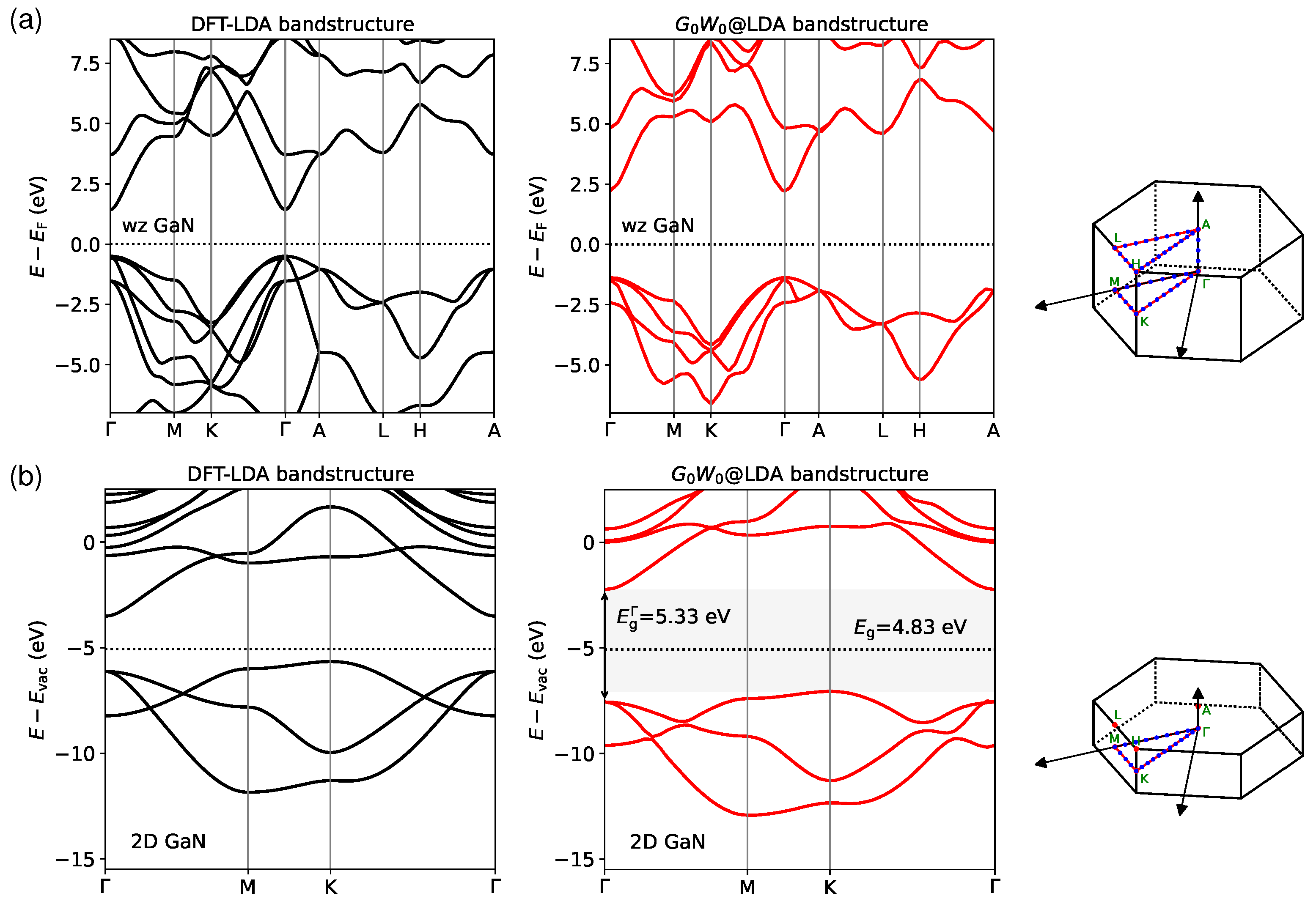
We present the bandstructures of both wurtzite and 2D GaN in Figure 5. It is shown that the bulk GaN has a clear direct band gap, both conduction band minimum (CBM) and valence band maximum (VBM) locating at the point (Figure 5a). This is consistent with previous studies [68,75,76]. In contrast, the 2D GaN appears to be an indirect band gap semiconductor according to our calculations. We note that the CBM occurs at , while the VBM locates at K (Figure 5b), which is in agreement with other calculations [36,37]. However, it may be noted that the direct gap at point () is not very far from the indirect gap (difference within eV), such that the 2D GaN has also been reported to exhibit a direct band gap in some other studies [38,77]. Additionally, it is worth mentioning that the 2D crystal undergoes a structural change from planar to buckled geometry due to H passivation [78]. The phase change could induce a transition from indirect to direct and an increased band gap [13,78].
The correction of over DFT can be simply interpreted as shifting the conduction bands upward while pushing the valence bands downward. Consequently, the size of the band gap is increased considerably, regardless of whether the band edges occur at the same k-point. On the other hand, does not alter the positions of the top of the valence band and the bottom of the conduction band in the Brillouin zone for both materials. We stress that the one-shot method has a disturbing starting point dependence, and the same issue also appears in the -BSE formalism. The good accuracy of @LDA should be partially attributed to a systematic underscreening due to the omission of vertex correction and an overscreening caused by the underestimation of the band gap by LDA, which tends to produce an error cancellation [79].
3.3. Excitons
The imaginary part of the dielectric function of the bulk GaN is shown in Figure 6. As it turns out, the BSE spectra (Figure 6a) with both in-plane () and out-of-plane polarization () are in general consistent with previous ab initio calculations [11]. Due to the lack of screened interactions, the RPA method leads to a sizable shift in the spectra toward higher energy. We zoom in on the spectra in the photon energy range of interest (– eV) in Figure 6b. They show that the onset of exciton peak due to electron–hole (e–h) excitation in RPA spectrum occurs at the direct band gap , which means that the e–h pair is completely not bound. The reason is that RPA does not include direct e–h interactions W, which could be inferred from Equation (5). As a consequence, RPA corresponds to a non-interacting picture, where only bare VB→CB transitions could be captured. In contrast, BSE predicts a pronounced excitonic effect, namely, an excitonic state well below the electronic band gap (Figure 6b). We find that the lowest excitonic level is well in agreement with the experimental photoluminescence excitation spectra [80,81], although the resulting exciton binding energy ( eV) is notably larger than expected.
To illustrate how the SOC effect can tune the optical response properties, we restricted it to the minimal transition space consisting of merely the topmost occupied band and the lowest unoccupied band (two-band approximation), and performed the BSE calculations switching on SOC. The results are shown in Figure 6c. We can see that when SOC is absent, the lowest bound exciton disappears. It indicates that the two-band model may not be reliable for bulk materials calculations. Interestingly, the inclusion of SOC could partially reproduce the multi-band results. In particular, the spin–orbit splitting nearly coincides with the lowest two excitons (Figure 6b), one of which occurs below the band gap while the other is located above it. This means that the influence of SOC on optical spectra is largely masked in bulk GaN.
In 2D GaN, the excitonic effects are much more significant compared to the hexagonal bulk GaN. Our BSE calculations predict a binding energy of eV for the lowest energy exciton (see Figure 7a). The result agrees well with other calculations using the sophisticated -BSE method [36,38]. Due to reduced dimensionality, the lowest excitonic peak is shifted toward the deep ultraviolet range, as demonstrated by an experiment on ultra-thin GaN/AlN heterostructures [14]. Meanwhile, the exciton binding energy turns out to be considerably larger as compared to that of bulk crystals [11], which may allow the stable existence of excitons at room temperature. This effect should be attributed to the reduced screening in the monolayer structure, which was pointed out in a previous study [38]. Even though the direct e–h interactions are absent in the RPA method, it seems that the RPA spectrum does not differ significantly from the BSE spectrum in bulk materials. However, in 2D GaN, the non-interacting picture simply does not work. We see that no evident absorption peaks are observed around the direct band gap, indicating that the screening effects are largely suppressed due to reduced dimensionality.
While it is reasonable to evaluate by solving BSE even without the scissors operator [82], the corresponding optical spectra would deviate dramatically from experiment. We anticipate that can be estimated from the GLLBSC functional for direct gap materials, such that both and the spectra comparable to the experiment could be obtained at a relatively low computational cost.
Again, we attempt to discuss the effect of SOC on the optical spectrum of 2D GaN in terms of the two-band model. It has be identified that the spin–orbit splitting is not visible in bulk GaN (tens of meV) [43], while in the 2D material, the SOC gives rise to A and B excitons separated by eV, as shown in Figure 7b. We stress that the splitting of excitonic peaks is not buried in the multi-band spectrum, suggesting that the SOC effect cannot be neglected when studying the 2D GaN.
4. Conclusions
By performing the many-body calculations, we found that the material undergoes a direct-to-indirect band gap transition from the bulk wurtzite structure to 2D GaN, and the quasiparticle band gap is increased by more than eV. This should be attributed to the strict quantum confinement that is intrinsic in nanomaterials. We have shown that both the exciton binding energy and the optical spectra given by the -BSE combination could be well reproduced by BSE calculations starting from Kohn–Sham eigenstates corrected by a scissors operator. Based on optical spectra obtained with (BSE) and without (RPA) direct electron–hole interactions, we show that the strong excitonic effect in 2D GaN originates from largely reduced dielectric screening due to low dimensionality compared to its bulk counterpart. On the other hand, the change in quasiparticle bandstructures and the tightly bound exciton considerably modify the absorption spectrum, indicating their strikingly different light-harvesting behaviors. Additionally, within the two-band approximation, we have demonstrated that the spin–orbit coupling could give rise to a splitting of excitonic peaks in 2D GaN.
Funding
This work was partly supported by the National Natural Science Foundation of China (NSFC) under Grant No. 22063002.
Data Availability Statement
The data that support the findings of this study are available from the corresponding author upon reasonable request.
Conflicts of Interest
The author declares no conflict of interest.
Abbreviations
The following abbreviations are used in this manuscript:
| 2D | Two-dimensional |
| DFT | Density-functional theory |
| BSE | Bethe–Salpeter Equation |
| QP | Quasiparticle |
| RPA | Random-phase approximation |
| PPA | Plasmon-pole approximation |
| PW | Plane wave |
| CBM | Conduction band minimum |
| VBM | Valence band maximum |
| SOC | Spin–orbit coupling |
References
- Strite, S.; Morkoç, H. GaN, AlN, and InN: A review. J. Vac. Sci. Technol. B 1992, 10, 1237–1266. [Google Scholar] [CrossRef]
- Wu, J. When group-III nitrides go infrared: New properties and perspectives. J. Appl. Phys. 2009, 106, 011101. [Google Scholar] [CrossRef]
- Fu, W.Y.; Choi, H.W. Progress and prospects of III-nitride optoelectronic devices adopting lift-off processes. J. Appl. Phys. 2022, 132, 060903. [Google Scholar] [CrossRef]
- Yamada, M.; Mitani, T.; Narukawa, Y.; Shioji, S.; Niki, I.; Sonobe, S.; Deguchi, K.; Sano, M.; Mukai, T. InGaN-Based Near-Ultraviolet and Blue-Light-Emitting Diodes with High External Quantum Efficiency Using a Patterned Sapphire Substrate and a Mesh Electrode. Jpn. J. Appl. Phys. 2002, 41, L1431. [Google Scholar] [CrossRef]
- Mi, Z.; Zhao, S. Extending group-III nitrides to the infrared: Recent advances in InN. Phys. Status Solidi B 2015, 252, 1050–1062. [Google Scholar] [CrossRef]
- Nakamura, S.; Pearton, S.; Fasol, G. The Blue Laser Diode: The Complete Story; Springer: Berlin/Heidelberg, Germany, 2000. [Google Scholar] [CrossRef]
- Pushpakaran, B.N.; Subburaj, A.S.; Bayne, S.B. Commercial GaN-Based Power Electronic Systems: A Review. J. Electron. Mater. 2020, 49, 6247. [Google Scholar] [CrossRef]
- Musa, A.Z.; Isa, M.M.; Ahmad, N.; Taking, S.; Musa, F.A. Normally-off GaN HEMT for high power and high-frequency applications. AIP Conf. Proc. 2021, 2347, 020121. [Google Scholar] [CrossRef]
- Bermudez, V. The fundamental surface science of wurtzite gallium nitride. Surf. Sci. Rep. 2017, 72, 147–315. [Google Scholar] [CrossRef]
- Mohanty, S.; Khan, K.; Ahmadi, E. N-polar GaN: Epitaxy, properties, and device applications. Prog. Quant. Electron. 2023, 87, 100450. [Google Scholar] [CrossRef]
- Laskowski, R.; Christensen, N.E.; Santi, G.; Ambrosch-Draxl, C. Ab initio calculations of excitons in GaN. Phys. Rev. B 2005, 72, 035204. [Google Scholar] [CrossRef]
- Adachi, K.; Ogi, H.; Nagakubo, A.; Nakamura, N.; Hirao, M.; Imade, M.; Yoshimura, M.; Mori, Y. Elastic constants of GaN between 10 and 305 K. J. Appl. Phys. 2016, 119, 245111. [Google Scholar] [CrossRef]
- Al Balushi, Z.Y.; Wang, K.; Ghosh, R.K.; Vilá, R.A.; Eichfeld, S.M.; Caldwell, J.D.; Qin, X.; Lin, Y.C.; DeSario, P.A.; Stone, G.; et al. Two-dimensional gallium nitride realized via graphene encapsulation. Nat. Mater. 2016, 15, 1166. [Google Scholar] [CrossRef] [PubMed]
- Bayerl, D.; Islam, S.; Jones, C.M.; Protasenko, V.; Jena, D.; Kioupakis, E. Deep ultraviolet emission from ultra-thin GaN/AlN heterostructures. Appl. Phys. Lett. 2016, 109, 241102. [Google Scholar] [CrossRef]
- Alaal, N.; Roqan, I.S. Tuning the Electronic Properties of Hexagonal Two-Dimensional GaN Monolayers via Doping for Enhanced Optoelectronic Applications. ACS Appl. Nano Mater. 2019, 2, 202–213. [Google Scholar] [CrossRef] [Green Version]
- Geim, A.K.; Grigorieva, I.V. Van der Waals heterostructures. Nature 2013, 499, 419. [Google Scholar] [CrossRef] [PubMed] [Green Version]
- Attia, A.A.; Jappor, H.R. Tunable electronic and optical properties of new two-dimensional GaN/BAs van der Waals heterostructures with the potential for photovoltaic applications. Chem. Phys. Lett. 2019, 728, 124–131. [Google Scholar] [CrossRef]
- Sang, L.; Sumiya, M.; Liao, M.; Koide, Y.; Yang, X.; Shen, B. Polarization-induced hole doping for long-wavelength In-rich InGaN solar cells. Appl. Phys. Lett. 2021, 119, 202103. [Google Scholar] [CrossRef]
- Aggarwal, N.; Gupta, G. Enlightening gallium nitride-based UV photodetectors. J. Mater. Chem. C 2020, 8, 12348–12354. [Google Scholar] [CrossRef]
- Moun, M.; Kumar, M.; Garg, M.; Pathak, R. Understanding of MoS2/GaN Heterojunction Diode and its Photodetection Properties. Sci. Rep. 2018, 8, 11799. [Google Scholar] [CrossRef] [Green Version]
- Goswami, L.; Aggarwal, N.; Vashishtha, P.; Jain, S.; Nirantar, S.; Ahmed, J.; Khan, M.; Pandey, R.; Gupta, G. Fabrication of GaN nano-towers based self-powered UV photodetector. Sci. Rep. 2021, 11, 10859. [Google Scholar] [CrossRef]
- Roldán, R.; Chirolli, L.; Prada, E.; Silva-Guillén, J.A.; San-Jose, P.; Guinea, F. Theory of 2D crystals: Graphene and beyond. Chem. Soc. Rev. 2017, 46, 4387–4399. [Google Scholar] [CrossRef] [Green Version]
- Thygesen, K.S. Calculating excitons, plasmons, and quasiparticles in 2D materials and van der Waals heterostructures. 2D Mater. 2017, 4, 022004. [Google Scholar] [CrossRef]
- Onida, G.; Reining, L.; Rubio, A. Electronic Excitations: Density-Functional versus Many-Body Green’s-Function Approaches. Rev. Mod. Phys. 2002, 74, 601–659. [Google Scholar] [CrossRef] [Green Version]
- Blase, X.; Duchemin, I.; Jacquemin, D.; Loos, P.F. The Bethe-Salpeter Equation Formalism: From Physics to Chemistry. J. Phys. Chem. Lett. 2020, 11, 7371–7382. [Google Scholar] [CrossRef] [PubMed]
- Vorwerk, C.; Aurich, B.; Cocchi, C.; Draxl, C. Bethe-Salpeter equation for absorption and scattering spectroscopy: Implementation in the exciting code. Electron. Struct. 2019, 1, 037001. [Google Scholar] [CrossRef]
- Crowley, J.M.; Tahir-Kheli, J.; Goddard, W.A. Resolution of the Band Gap Prediction Problem for Materials Design. J. Phys. Chem. Lett. 2016, 7, 1198–1203. [Google Scholar] [CrossRef]
- Perdew, J.P.; Levy, M. Physical Content of the Exact Kohn-Sham Orbital Energies: Band Gaps and Derivative Discontinuities. Phys. Rev. Lett. 1983, 51, 1884–1887. [Google Scholar] [CrossRef]
- Mori-Sánchez, P.; Cohen, A.J.; Yang, W. Localization and Delocalization Errors in Density Functional Theory and Implications for Band-Gap Prediction. Phys. Rev. Lett. 2008, 100, 146401. [Google Scholar] [CrossRef] [PubMed] [Green Version]
- Rasmussen, F.A.; Thygesen, K.S. Computational 2D Materials Database: Electronic Structure of Transition-Metal Dichalcogenides and Oxides. J. Phys. Chem. C 2015, 119, 13169–13183. [Google Scholar] [CrossRef]
- Yakovkin, I.N. Dirac Cones in Graphene, Interlayer Interaction in Layered Materials, and the Band Gap in MoS2. Crystals 2016, 6, 143. [Google Scholar] [CrossRef] [Green Version]
- Rasmussen, F.A.; Schmidt, P.S.; Winther, K.T.; Thygesen, K.S. Efficient many-body calculations for two-dimensional materials using exact limits for the screened potential: Band gaps of MoS2, h-BN, and phosphorene. Phys. Rev. B 2016, 94, 155406. [Google Scholar] [CrossRef] [Green Version]
- Haastrup, S.; Strange, M.; Pandey, M.; Deilmann, T.; Schmidt, P.S.; Hinsche, N.F.; Gjerding, M.N.; Torelli, D.; Larsen, P.M.; Riis-Jensen, A.C.; et al. The Computational 2D Materials Database: High-throughput modeling and discovery of atomically thin crystals. 2D Mater. 2018, 5, 042002. [Google Scholar] [CrossRef]
- Massicotte, M.; Vialla, F.; Schmidt, P.; Lundeberg, M.B.; Latini, S.; Haastrup, S.; Danovich, M.; Davydovskaya, D.; Watanabe, K.; Taniguchi, T.; et al. Dissociation of two-dimensional excitons in monolayer WSe2. Nat. Commun. 2018, 9, 1633. [Google Scholar] [CrossRef] [PubMed] [Green Version]
- Sanders, N.; Bayerl, D.; Shi, G.; Mengle, K.A.; Kioupakis, E. Electronic and Optical Properties of Two-Dimensional GaN from First-Principles. Nano Lett. 2017, 17, 7345–7349. [Google Scholar] [CrossRef] [PubMed]
- Peng, B.; Zhang, H.; Shao, H.; Xu, K.; Ni, G.; Wu, L.; Li, J.; Lu, H.; Jin, Q.; Zhu, H. Room-Temperature Bound Exciton with Long Lifetime in Monolayer GaN. ACS Photonics 2018, 5, 4081–4088. [Google Scholar] [CrossRef]
- Shu, H.; Niu, X.; Ding, X.; Wang, Y. Effects of strain and surface modification on stability, electronic and optical properties of GaN monolayer. Appl. Surf. Sci. 2019, 479, 475–481. [Google Scholar] [CrossRef]
- Prete, M.S.; Grassano, D.; Pulci, O.; Kupchak, I.; Olevano, V.; Bechstedt, F. Giant excitonic absorption and emission in two-dimensional group-III nitrides. Sci. Rep. 2020, 10, 10719. [Google Scholar] [CrossRef]
- Andersen, K.; Latini, S.; Thygesen, K.S. Dielectric Genome of van der Waals Heterostructures. Nano Lett. 2015, 15, 4616–4621. [Google Scholar] [CrossRef] [Green Version]
- Latini, S.; Winther, K.T.; Olsen, T.; Thygesen, K.S. Interlayer Excitons and Band Alignment in MoS2/hBN/WSe2 van der Waals Heterostructures. Nano Lett. 2017, 17, 938–945. [Google Scholar] [CrossRef] [Green Version]
- Elliott, J.D.; Colonna, N.; Marsili, M.; Marzari, N.; Umari, P. Koopmans Meets Bethe–Salpeter: Excitonic Optical Spectra without GW. J. Chem. Theory Comput. 2019, 15, 3710–3720. [Google Scholar] [CrossRef] [Green Version]
- Li, J.; Jin, Y.; Su, N.Q.; Yang, W. Combining localized orbital scaling correction and Bethe-Salpeter equation for accurate excitation energies. J. Chem. Phys. 2022, 156, 154101. [Google Scholar] [CrossRef]
- Orton, J.W. Exciton spectra and spin-orbit splitting in GaN epitaxial films. Semicond. Sci. Technol. 1997, 12, 64. [Google Scholar] [CrossRef]
- Ren, G.B.; Liu, Y.M.; Blood, P. Valence-band structure of wurtzite GaN including the spin-orbit interaction. Appl. Phys. Lett. 1999, 74, 1117–1119. [Google Scholar] [CrossRef]
- Jhalani, V.A.; Chen, H.Y.; Palummo, M.; Bernardi, M. Precise radiative lifetimes in bulk crystals from first principles: The case of wurtzite gallium nitride. J. Phys. Condens. Matter 2019, 32, 084001. [Google Scholar] [CrossRef]
- Enkovaara, J.; Rostgaard, C.; Mortensen, J.J.; Chen, J.; Dułak, M.; Ferrighi, L.; Gavnholt, J.; Glinsvad, C.; Haikola, V.; Hansen, H.A.; et al. Electronic Structure Calculations with GPAW: A Real-Space Implementation of the Projector Augmented-Wave Method. J. Phys. Condens. Matter 2010, 22, 253202. [Google Scholar] [CrossRef] [PubMed]
- Blöchl, P.E. Projector Augmented-Wave Method. Phys. Rev. B 1994, 50, 17953. [Google Scholar] [CrossRef] [PubMed] [Green Version]
- Perdew, J.P.; Wang, Y. Accurate and Simple Analytic Representation of the Electron-Gas Correlation Energy. Phys. Rev. B 1992, 45, 13244–13249. [Google Scholar] [CrossRef] [PubMed]
- Perdew, J.P.; Burke, K.; Ernzerhof, M. Generalized Gradient Approximation Made Simple. Phys. Rev. Lett. 1996, 77, 3865–3868. [Google Scholar] [CrossRef] [Green Version]
- Hedin, L. New Method for Calculating the One-Particle Green’s Function with Application to the Electron-Gas Problem. Phys. Rev. 1965, 139, A796–A823. [Google Scholar] [CrossRef]
- Aryasetiawan, F.; Gunnarsson, O. The GW method. Rep. Prog. Phys. 1998, 61, 237–312. [Google Scholar] [CrossRef] [Green Version]
- Hybertsen, M.S.; Louie, S.G. Electron correlation in semiconductors and insulators: Band gaps and quasiparticle energies. Phys. Rev. B 1986, 34, 5390–5413. [Google Scholar] [CrossRef] [PubMed]
- Hüser, F.; Olsen, T.; Thygesen, K.S. Quasiparticle GW calculations for solids, molecules, and two-dimensional materials. Phys. Rev. B 2013, 87, 235132. [Google Scholar] [CrossRef] [Green Version]
- Rasmussen, A.; Deilmann, T.; Thygesen, K.S. Towards fully automated GW band structure calculations: What we can learn from 60.000 self-energy evaluations. npj Comput. Mater. 2021, 7, 22. [Google Scholar] [CrossRef]
- Yan, J.; Jacobsen, K.W.; Thygesen, K.S. Optical properties of bulk semiconductors and graphene/boron nitride: The Bethe-Salpeter equation with derivative discontinuity-corrected density functional energies. Phys. Rev. B 2012, 86, 045208. [Google Scholar] [CrossRef] [Green Version]
- Salpeter, E.E.; Bethe, H.A. A Relativistic Equation for Bound-State Problems. Phys. Rev. 1951, 84, 1232–1242. [Google Scholar] [CrossRef]
- Latini, S. Excitons in van der Waals Heterostructures: A Theoretical Study. Ph.D. Thesis, Technical University of Denmark, Kongens Lyngby, Denmark, 2016. [Google Scholar]
- Olsen, T. Designing in-plane Heterostructures of Quantum Spin Hall Insulators from First Principles: 1T′-MoS2 with Adsorbates. Phys. Rev. B 2016, 94, 235106. [Google Scholar] [CrossRef] [Green Version]
- Alchagirov, A.B.; Perdew, J.P.; Boettger, J.C.; Albers, R.C.; Fiolhais, C. Energy and pressure versus volume: Equations of state motivated by the stabilized jellium model. Phys. Rev. B 2001, 63, 224115. [Google Scholar] [CrossRef]
- Larsen, A.H.; Mortensen, J.J.; Blomqvist, J.; Castelli, I.E.; Christensen, R.; Dułak, M.; Friis, J.; Groves, M.N.; Hammer, B.; Hargus, C.; et al. The atomic simulation environment—A Python library for working with atoms. J. Phys. Condens. Matter 2017, 29, 273002. [Google Scholar] [CrossRef] [Green Version]
- Magnuson, M.; Mattesini, M.; Höglund, C.; Birch, J.; Hultman, L. Electronic structure of GaN and Ga investigated by soft x-ray spectroscopy and first-principles methods. Phys. Rev. B 2010, 81, 085125. [Google Scholar] [CrossRef] [Green Version]
- Rosa, A.L.; Neugebauer, J. First-principles calculations of the structural and electronic properties of clean GaN (0001) surfaces. Phys. Rev. B 2006, 73, 205346. [Google Scholar] [CrossRef]
- Maniš, J.; Mach, J.; Bartošík, M.; Šamořil, T.; Horák, M.; Čalkovský, V.; Nezval, D.; Kachtik, L.; Konečný, M.; Šikola, T. Low temperature 2D GaN growth on Si(111) 7 × 7 assisted by hyperthermal nitrogen ions. Nanoscale Adv. 2022, 4, 3549–3556. [Google Scholar] [CrossRef] [PubMed]
- Onen, A.; Kecik, D.; Durgun, E.; Ciraci, S. GaN: From three- to two-dimensional single-layer crystal and its multilayer van der Waals solids. Phys. Rev. B 2016, 93, 085431. [Google Scholar] [CrossRef]
- Hüser, F.; Olsen, T.; Thygesen, K.S. How dielectric screening in two-dimensional crystals affects the convergence of excited-state calculations: Monolayer MoS2. Phys. Rev. B 2013, 88, 245309. [Google Scholar] [CrossRef] [Green Version]
- Latini, S.; Olsen, T.; Thygesen, K.S. Excitons in van der Waals heterostructures: The important role of dielectric screening. Phys. Rev. B 2015, 92, 245123. [Google Scholar] [CrossRef] [Green Version]
- Ullah, S.S.; Farooq, M.; Din, H.U.; Alam, Q.; Idrees, M.; Bilal, M.; Amin, B. First principles study of electronic and optical properties and photocatalytic performance of GaN-SiS van der Waals heterostructure. RSC Adv. 2021, 11, 32996–33003. [Google Scholar] [CrossRef]
- Rubio, A.; Corkill, J.L.; Cohen, M.L.; Shirley, E.L.; Louie, S.G. Quasiparticle band structure of AlN and GaN. Phys. Rev. B 1993, 48, 11810–11816. [Google Scholar] [CrossRef]
- Reimann, K.; Steube, M.; Fröhlich, D.; Clarke, S. Exciton binding energies and band gaps in GaN bulk crystals. J. Cryst. Growth 1998, 189–190, 652–655. [Google Scholar] [CrossRef]
- Yeo, Y.C.; Chong, T.C.; Li, M.F. Electronic band structures and effective-mass parameters of wurtzite GaN and InN. J. Appl. Phys. 1998, 83, 1429–1436. [Google Scholar] [CrossRef]
- Kuisma, M.; Ojanen, J.; Enkovaara, J.; Rantala, T.T. Kohn-Sham potential with discontinuity for band gap materials. Phys. Rev. B 2010, 82, 115106. [Google Scholar] [CrossRef] [Green Version]
- Zhang, Y. Photocatalytic activity of MoS2 with water monolayers: Global optimization. J. Chem. Phys. 2022, 157, 184703. [Google Scholar] [CrossRef]
- Chaves, A.; Azadani, J.G.; Alsalman, H.; da Costa, D.R.; Frisenda, R.; Chaves, A.J.; Song, S.H.; Kim, Y.D.; He, D.; Zhou, J.; et al. Bandgap engineering of two-dimensional semiconductor materials. npj 2D Mater. Appl. 2020, 4, 29. [Google Scholar] [CrossRef]
- Ben, J.; Liu, X.; Wang, C.; Zhang, Y.; Shi, Z.; Jia, Y.; Zhang, S.; Zhang, H.; Yu, W.; Li, D.; et al. 2D III-Nitride Materials: Properties, Growth, and Applications. Adv. Mater. 2021, 33, 2006761. [Google Scholar] [CrossRef] [PubMed]
- Goano, M.; Bellotti, E.; Ghillino, E.; Ghione, G.; Brennan, K.F. Band structure nonlocal pseudopotential calculation of the III-nitride wurtzite phase materials system. Part I. Binary compounds GaN, AlN, and InN. J. Appl. Phys. 2000, 88, 6467–6475. [Google Scholar] [CrossRef]
- Poncé, S.; Jena, D.; Giustino, F. Hole mobility of strained GaN from first principles. Phys. Rev. B 2019, 100, 085204. [Google Scholar] [CrossRef] [Green Version]
- Prete, M.S.; Mosca Conte, A.; Gori, P.; Bechstedt, F.; Pulci, O. Tunable electronic properties of two-dimensional nitrides for light harvesting heterostructures. Appl. Phys. Lett. 2017, 110, 012103. [Google Scholar] [CrossRef]
- Dong, Y.; Li, E.; Cui, Z.; Shen, Y.; Ma, D.; Wang, F.; Yuan, Z.; Yang, K. Electronic properties and photon scattering of buckled and planar few-layer 2D GaN. Vacuum 2023, 210, 111861. [Google Scholar] [CrossRef]
- Li, J.; Jin, Y.; Rinke, P.; Yang, W.; Golze, D. Benchmark of GW Methods for Core-Level Binding Energies. J. Chem. Theory Comput. 2022, 18, 7570–7585. [Google Scholar] [CrossRef]
- Kovalev, D.; Averboukh, B.; Volm, D.; Meyer, B.K.; Amano, H.; Akasaki, I. Free exciton emission in GaN. Phys. Rev. B 1996, 54, 2518–2522. [Google Scholar] [CrossRef]
- Hägele, D.; Zimmermann, R.; Oestreich, M.; Hofmann, M.; Rühle, W.; Meyer, B.; Amano, H.; Akasaki, I. Energy loss rate of excitons in GaN. Physica B 1999, 272, 409–411. [Google Scholar] [CrossRef]
- Olsen, T.; Latini, S.; Rasmussen, F.; Thygesen, K.S. Simple Screened Hydrogen Model of Excitons in Two-Dimensional Materials. Phys. Rev. Lett. 2016, 116, 056401. [Google Scholar] [CrossRef] [Green Version]
Figure 1.
Schematic band edge diagram illustrating the exciton binding energy , which can be calculated as the difference between fundamental gap and optical gap . The latter refers to the position of lowest exciton peak (photon energy ) in optical absorption spectrum. One can evaluate optical gaps from eigenvalues of excitons by solving the Bethe–Salpeter equation.

Figure 2.
Top and side view of the supercell of the wurtzite GaN (left) and the slab model of the 2D GaN (right).
Figure 2.
Top and side view of the supercell of the wurtzite GaN (left) and the slab model of the 2D GaN (right).

Figure 3.
Total energy of the wurtzite GaN as a function of the compression ratio. Here, V is the unit cell volume calculated by , and is the initial cell volume with the experimental lattice constant Å. The lines are obtained by fitting the DFT data points with the equation of state, , where . The minimal energy of each potential energy curve is shifted to zero. The equilibrium ratios are 1.005 and 1.061 for LDA and PBE, respectively.

Figure 4.
Convergence test for the quasiparticle band gap of (a) wurtzite and (b) 2D GaN produced by G0W0@LDA with respect to k-points grid. The ecut represents plane wave cutoff in self-energy calculations, and PPA refers to the Godby–Needs plasmon-pole approximation used in calculating the dielectric function.

Figure 5.
Bandstructures of (a) wurtzite (wz) and (b) 2D GaN calculated by both DFT-LDA and @LDA methods. The corrections are performed on the top 4 valence bands and lowest 4 conduction bands in both materials, and a spline interpolation is used for smoothing. A schematic of special k-points along given band paths in the Brillouin zone is shown on the right side. The dotted line refers to the Fermi energy . The energy levels are aligned with respect to for bulk GaN, while for 2D GaN, absolute band positions are presented with the vacuum level shifted to 0 eV.

Figure 6.
(a) Calculated imaginary part of dielectric functions of wurtzite GaN as a function of photon energy using BSE and RPA methods. and indicate in-plane and out-of-plane light polarization, respectively. A Lorentzian broadening of eV is used to generate the spectrum. The top four valence bands and lowest four conduction bands are included to construct the transition space. (b) The resulting in a smaller energy window with a broadening parameter of eV. (c) BSE calculated spectrum for a transition space consisting of only the topmost valence band and lowest conduction band with and without spin–orbit coupling (SOC). A scissors operator of eV is applied for these calculations.

Figure 7.
(a) Absorption spectra of 2D GaN calculated within BSE and RPA for the incoming light polarization parallel to the atomic layer. The vertical line indicates the direct band gap at the point, . (b) BSE spectrum with and without SOC in a transition space containing only the highest occupied band and lowest unoccupied band. These spectra were generated with a broadening width of eV and a scissors operator of eV.

Disclaimer/Publisher’s Note: The statements, opinions and data contained in all publications are solely those of the individual author(s) and contributor(s) and not of MDPI and/or the editor(s). MDPI and/or the editor(s) disclaim responsibility for any injury to people or property resulting from any ideas, methods, instructions or products referred to in the content. |
© 2023 by the author. Licensee MDPI, Basel, Switzerland. This article is an open access article distributed under the terms and conditions of the Creative Commons Attribution (CC BY) license (https://creativecommons.org/licenses/by/4.0/).
Share and Cite
MDPI and ACS Style
Zhang, Y. Many-Body Calculations of Excitons in Two-Dimensional GaN. Crystals 2023, 13, 1048. https://0-doi-org.brum.beds.ac.uk/10.3390/cryst13071048
AMA Style
Zhang Y. Many-Body Calculations of Excitons in Two-Dimensional GaN. Crystals. 2023; 13(7):1048. https://0-doi-org.brum.beds.ac.uk/10.3390/cryst13071048
Chicago/Turabian StyleZhang, Yachao. 2023. "Many-Body Calculations of Excitons in Two-Dimensional GaN" Crystals 13, no. 7: 1048. https://0-doi-org.brum.beds.ac.uk/10.3390/cryst13071048
Note that from the first issue of 2016, this journal uses article numbers instead of page numbers. See further details here.