Fabrication of GaOx Confinement Structure for InGaN Light Emitter Applications
by

Yi-Yun Chen
1, 
Yuan-Chang Jhang
1,
Chia-Jung Wu
1,
Hsiang Chen
2,
Yung-Sen Lin
3 and
Chia-Feng Lin
1,* 1
Department of Materials Science and Engineering, Innovation and Development Center of Sustainable Agriculture, Research Center for sustainable energy and Nanotechnology, National Chung Hsing University, No. 145, Xingda Road, South Dist., Taichung 402, Taiwan
2
Department of Applied Materials and Optoelectronic Engineering, National Chi Nan University, No. 1, University Road, Puli Township, Nantou County 545, Taiwan
3
Department of Chemical Engineering, Feng Chia University, No. 100, Wenhwa Road, Seatwen, Taichung 40724, Taiwan
*
Author to whom correspondence should be addressed.
Crystals 2018, 8(11), 418; https://0-doi-org.brum.beds.ac.uk/10.3390/cryst8110418
Submission received: 29 September 2018
/
Revised: 2 November 2018
/
Accepted: 4 November 2018
/
Published: 7 November 2018
(This article belongs to the Special Issue Functional Oxide Based Thin-Film Materials)
Abstract
:An indium gallium nitride (InGaN) light-emitting diode (LED) with an embedded porous GaN reflector and a current confined aperture is presented in this study. Eight pairs of n+-GaN:Si/GaN in stacked structure are transformed into a conductive, porous GaN/GaN reflector through an electrochemical wet-etching process. Porous GaN layers surrounding the mesa region were transformed into insulating GaOx layers in a reflector structure through a lateral photoelectrochemical (PEC) oxidation process. The electroluminescence emission intensity was localized at the central mesa region by forming the insulating GaOx layers in a reflector structure as a current confinement aperture structure. The PEC-LED structure with a porous GaN reflector and a current-confined aperture surrounded by insulating GaOx layers has the potential for nitride-based resonance cavity light source applications.
1. Introduction
Gallium nitride (GaN) materials have been developed for optoelectronic devices such as light-emitting diodes (LEDs), laser diodes (LD) [1], and vertical cavity surface emitting lasers (VCSEL) [2]. Lateral oxidation of high aluminum (Al) content AlGaAs-based epilayers [3,4] produces a current-confining aperture in the central microcavity structure. The lateral oxidized process was used to transform AlAs into insulating AlOx, acting as a current confinement aperture in the microcavity structure [5]. For nitride materials, Dorsaz et al. [6] reported the use of the electrochemical oxidation process for AlInN to form current apertures. The epitaxial AlGaN/GaN stack [7], AlN/GaN stacks [8,9], and AlInN/GaN stack [10] structures have been reported for bottom epitaxial distributed Bragg reflector (DBR) in GaN-based VCSEL devices. Here, an InGaN-based LED structure with n-GaN:Si/GaN stack epi-layers is transformed into a conductive porous-GaN/GaN reflector through a wet electrochemical (EC) etching process. Then, the porous GaN layers surrounding the mesa region are transformed into insulating GaOx layers in the stack structure through a photoelectrochemical (PEC) oxidation process. A current-confined aperture in the bottom porous GaN reflector was produced in the central mesa region.
2. Experimental
The LED epitaxial layer consisted of a 30 nm-thick GaN buffer layer grown at 530 °C, a 2.0 µm-thick unintentionally doped GaN layer (u-GaN, 1050 °C, 5 × 1016 cm−3), a 1.0 µm-thick n-GaN layer (1050 °C, 2 × 1018 cm−3) for the bottom n-type contact layer, eight pairs of n+-GaN:Si/GaN (n+-GaN:Si with 2 × 1019 cm−3) stack structure, a 0.2 µm-thick u-GaN layer (1050 °C), a 0.3 µm-thick n-GaN layer (1050 °C, 2 × 1018 cm−3), six pairs of In0.2GaN/GaN (3 nm/12 nm) multiple quantum wells (MQWs, 760 °C), and a 0.1 µm-thick p-GaN layer (950 °C, 1 × 1018 cm−3). A 150 nm-thick indium tin oxide (ITO) film was deposited on the mesa region and acted as a transparent conductive layer. The mesa regions of the InGaN LED structures were defined using a laser scribing (LS) process and dry etching process with a 1.5 µm etching depth to produce the as-grown eight-period n+-GaN/GaN stack structure. The LED chips were 35 × 35 µm2 in size, and the mesa regions were defined by using a triple frequency ultraviolet Nd:YVO4 (355 nm) laser for the front side laser scribing process with a 40 µm spacing width. The samples were immersed in a 0.5 M nitride acid solution for wet electrochemical (EC) etching with an external direct current (DC) bias voltage of +8 V. The EC-treated LED structure with a porous GaN reflector was defined as an EC-LED. Then, the samples were oxidized through a PEC oxidation process with a +20 V bias voltage and illuminated with a 400 W Hg lamp in deionized water for 30 min [11,12]. The porous GaN/GaN stack reflector structure was transformed into a GaOx/GaN stack reflector. The PEC-treated LED with GaOx/GaN stack structure surrounding the mesa region was defined as a PEC-LED. The electroluminescence (EL) spectra were measured through an optical spectrum analyzer (iHR550, Edison, NJ, USA) and the light intensity profiles were measured by a beam profiler (Spiricon, Jerusalem, Israel).
3. Results and Discussions
The optical microscopy (OM) images of the standard-LED (ST-LED), electrochemical etch LED (EC-LED), and photoelectrochemical oxidized LED (PEC-LED) structures are shown in Figure 1a–c, respectively. After the EC wet etching process, the n+-GaN:Si/u-GaN stack structure was transformed into a porous GaN/GaN reflector as shown in Figure 1b. The n+-GaN:Si layers in the stack structure were etched to form the porous GaN layers. The laser scribing line patterns provided the wet etching channels on the n+-GaN:Si/GaN stack structure. The porous GaN reflector in the blue light range was observed on the mesa region. Then, the porous GaN/GaN reflector was transformed into a GaOx/GaN reflector through the PEC oxidation process. The PEC oxidized process occurred from the LS lines and formed the GaOx layers in the stack structure surrounding the mesa region.
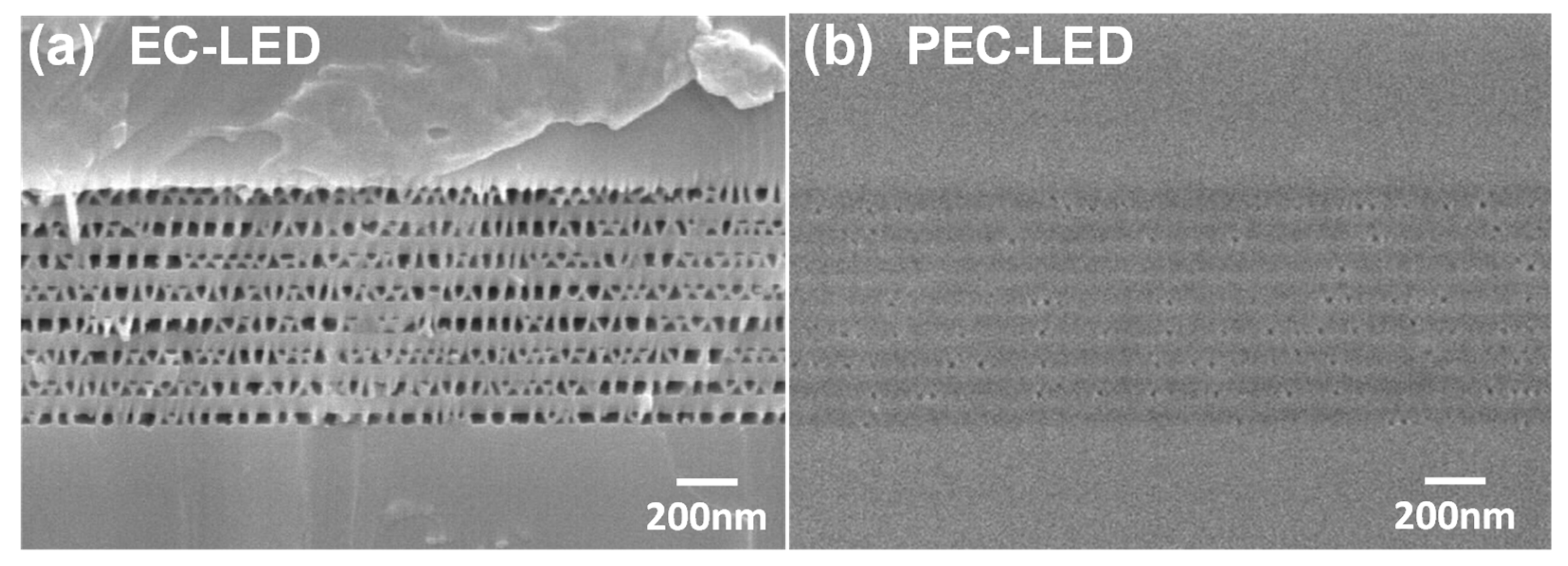
In Figure 2a, eight pairs of n+-GaN:Si/GaN stack structures were transformed into a porous GaN/GaN stack structure using the EC etching process. The pair thickness of n+-GaN:Si/GaN was about 102 nm. After the PEC oxidation process, the porous GaN layer was oxidized as a GaOx layer, as shown in Figure 2b. The GaN layers in the PEC-LED structure became thinner compared to in the EC-LED structure, indicating that part of the GaN layer was oxidized during the PEC oxidation process. The porous GaN layers in the stack structure provided a channel for the OH- ions to oxidize the residual single crystalline GaN in the porous structure. The GaOx/GaN stack structure was formed surrounding the mesa region through the lateral PEC oxidation process.
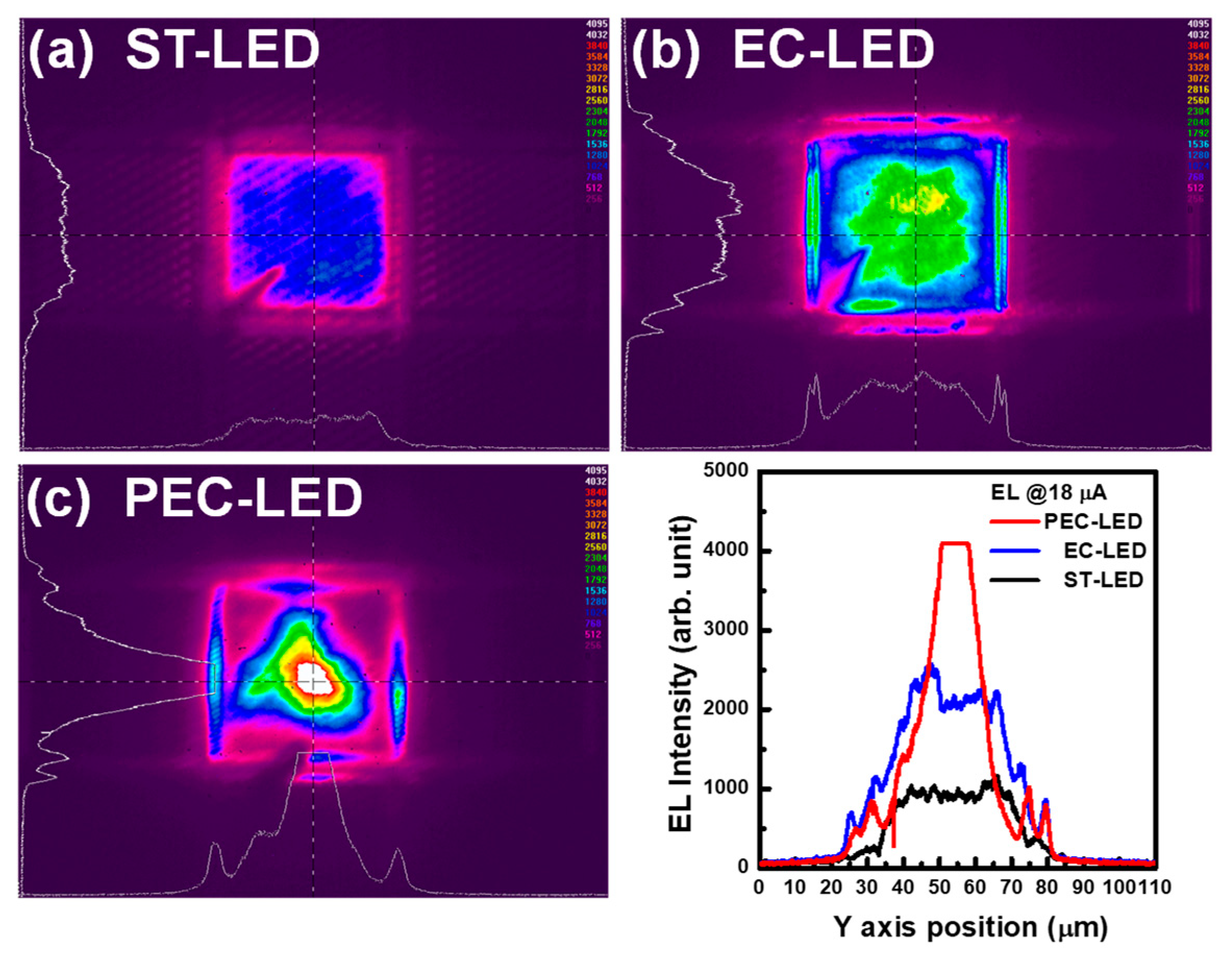
The EL (electroluminescence) emission images of the ST-LED, EC-LED, and PEC-LED are provided in Figure 3a–c, respectively, at an 18 μA injection current. In Figure 3a, the uniform emission intensity was observed in the mesa region of the ST-LED. High-EL emission intensity was observed in the EC-LED structure caused by the formation of a high-reflectivity porous GaN reflector (Figure 3b). In the PEC-LED structure, the high-EL emission intensity was localized in the central mesa region as shown in Figure 3c. This occurred because the insulating GaOx layers in the stack structure formed surrounding the mesa region after the lateral PEC oxidation process. The EL light was emitted from the central mesa region and was extracted from the mesa sidewall region. The line EL intensity profiles of the LED samples are observed. After the PEC process, the EL emission intensity of the PEC-LED was localized in the central mesa region. An InGaN-based LED with GaOx current confinement structure was produced via the EC etching process and the PEC oxidation process.
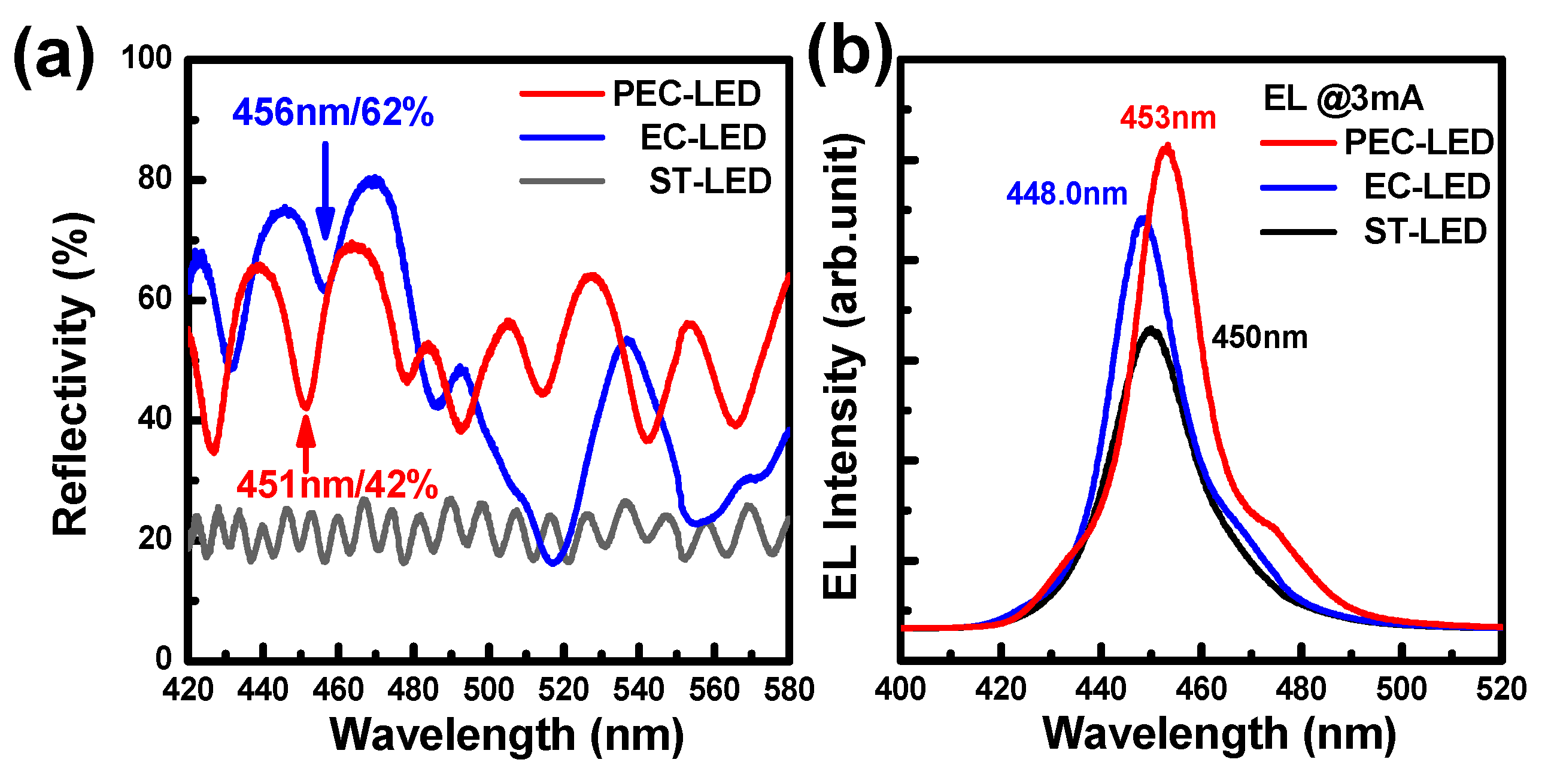
The reflectance spectra of the LED samples were measured as shown in Figure 4a. The light interference spectrum of the non-treated LED epi-structure was observed due to the light reflection between the top air/GaN:Mg and bottom GaN/sapphire interfaces. The reflectivity of the ST-LED was measured at about 20% as the reference spectrum. In the EC-LED structure, the high reflectance spectrum was observed at 469 nm/80% and 446 nm/76%, which dipped at 456 nm/62%. After the EC etching process, a 0.7 μm-thick InGaN LED cavity was formed between the top air/GaN interface and the bottom porous GaN reflector. The dip wavelength in the reflectance spectrum was caused by the light interference in the short cavity structure. In the PEC-LED structure, the peak reflectance spectrum was observed at 464 nm/69% and 439 nm/66%, which had a dip wavelength at 451 nm/42%. The central dip wavelength shifted from 456 nm (EC-LED) to 451 nm (PEC-LED) due to the transformation process from the porous GaN layers to the GaOx layers in the stack reflector structure. In Figure 4b, the EL peak wavelengths and linewidth were measured at 450 nm and 19.1 nm for the ST-LED, 448 nm/17.2 nm for the EC-LED, and 453 nm/16.5 nm for the PEC-LED structure, respectively, at a 3 mA operation current. The EL emission intensity of the EC-LED was higher than that of the ST-LED, caused by the formation of a highly reflective and conductive porous GaN reflector. The EL peak wavelength of the PEC-LED slightly redshifted compared to ST-LED, potentially caused by the thermal joule heat in the LED device at the high operating current density in the confinement aperture structure.
4. Conclusions
An InGaN LED structure with an embedded porous GaN reflector and a current-confined aperture was fabricated through the lateral EC etching and PEC oxidation processes. The central wavelength of the porous GaN reflector matched the EL emission spectrum. The porous GaN layers provided a large surface area for the following PEC oxidation process. The central wavelength of the reflectors was blueshifted by transforming the porous GaN/GaN stack structure into a GaOx/GaN stack structure. The injection current in the PEC-LED was confined to the aperture structure by being surrounded by insulating GaOx layers in the reflector structure. The produced PEC-LED structure with a porous GaN reflector and a current-confined aperture surrounding by insulating GaOx layers has the potential for nitride-based resonant-cavity LED device applications.
Author Contributions
Y.-Y.C., Y.-C.J. and C.-J.W. fabricated the EC-LED and PEC-LED. H.C. supporting the analysis of the LED samples. Y.-S.L. performed the EL measurement and analysis. C.-F.L. organized the experiment design and wrote the manuscript with contributed from other co-authors.
Funding
This research received no external funding.
Acknowledgments
The authors gratefully acknowledge the financial support for this research by the Ministry of Science and Technology of Taiwan under grant No. 105-2221-E-005-012-MY2 and 107-2221-E-005-061. It was further supported by the Innovation and Development Center of Sustainable Agriculture’s Featured Areas Research Center Program within the framework of Taiwan’s Ministry of Education’s Higher Education Sprout Project.
Conflicts of Interest
The authors declare no conflict of interest.
References
- Nakamura, S. The Roles of Structural Imperfections in InGaN-Based Blue Light-Emitting Diodes and Laser Diodes. Science 1998, 281, 956–961. [Google Scholar] [CrossRef] [Green Version]
- Someya, T.; Werner, R.; Forchel, A.; Catalano, M.; Cingolani, R.; Arakawa, Y. Room Temperature Lasing at Blue Wavelengths in Gallium Nitride Microcavities. Science 1999, 285, 1905–1906. [Google Scholar] [CrossRef] [PubMed]
- Yang, G.M.; MacDougal, M.H.; Dapkus, P.D. Ultralow Threshold Current Vertical-cavity Surface-emitting Lasers Obtained with Selective Oxidation. Electron. Lett. 1995, 31, 886–888. [Google Scholar] [CrossRef]
- Bissessur, H.K.; Koyama, F.; Iga, K. Modeling of Oxide-confined Vertical-cavity Surface-Emitting Lasers. IEEE J. Sel. Top. Quantum Electron. 1997, 3, 344–352. [Google Scholar] [CrossRef]
- MacDougal, M.H.; Dapkus, P.D.; Bond, A.E.; Lin, C.-K.; Geske, J. Design and Fabrication VCSEL’s with AlxOy–GaAs DBR’s. IEEE J. Sel. Top. Quantum Electron. 1997, 3, 905–915. [Google Scholar] [CrossRef]
- Dorsaz, J.; Bühlmann, H.J.; Carlin, J.F.; Grandjean, N.; Ilegems, M. Selective Oxidation of AlInN Layers for Current Confinement in III–nitride Devices. Appl. Phys. Lett. 2005, 87, 072102. [Google Scholar] [CrossRef]
- Nakada, N.; Nakaji, M.; Ishikawa, H.; Egawa, T.; Umeno, M.; Jimbo, T. Improved characteristics of InGaN multiple-quantum-well light-emitting diode by GaN/AlGaN distributed Bragg reflector grown on sapphire. Appl. Phys. Lett. 2000, 76, 1804–1806. [Google Scholar] [CrossRef]
- Lin, C.F.; Yao, H.H.; Lu, J.W.; Hsieh, Y.L.; Kuo, H.C.; Wang, S.C. Characteristics of Stable Emission GaN-Based Resonant-Cavity Light-Emitting Diodes. J. Cryst. Growth 2004, 261, 359–363. [Google Scholar] [CrossRef]
- Yao, H.H.; Lin, C.F.; Kuo, H.C.; Wang, S.C. MOCVD Growth of AlN/GaN DBR Structures under Various Ambient Conditions. J. Cryst. Growth 2004, 262, 151–156. [Google Scholar] [CrossRef]
- Carlin, J.F.; Ilegems, M. High-Quality AllnN for High Index Contrast Bragg Mirrors Lattice Matched to GaN. Appl. Phys. Lett. 2003, 83, 668–670. [Google Scholar] [CrossRef]
- Lin, C.F.; Yang, Z.J.; Zheng, J.H.; Dai, J.J. Enhanced Light Output in Nitride-based Light-emitting Diodes by Roughening the Mesa Sidewall. IEEE Photonics Technol. Lett. 2005, 17, 2038–2040. [Google Scholar]
- Lin, C.F.; Chen, K.T.; Huang, K.P. Blue Light-Emitting Diodes with an Embedded Native Gallium Oxide Pattern Structure. IEEE Electron Device Lett. 2010, 31, 1431–1433. [Google Scholar] [CrossRef]
Figure 1.
OM images of (a) ST-LED, (b) EC-LED, and (c) PEC-LED were observed with laser scribing line patterns. The mesa regions were 35 × 35 μm.
Figure 1.
OM images of (a) ST-LED, (b) EC-LED, and (c) PEC-LED were observed with laser scribing line patterns. The mesa regions were 35 × 35 μm.

Figure 2.
The SEM (scanning electron microscope) micrographs of (a) nanoporous GaN/GaN stack structure and (b) GaOx/GaN stack structure. The GaOx layer in the PEC-LED structure was prepared through the EC etching and PEC oxidized processes.
Figure 2.
The SEM (scanning electron microscope) micrographs of (a) nanoporous GaN/GaN stack structure and (b) GaOx/GaN stack structure. The GaOx layer in the PEC-LED structure was prepared through the EC etching and PEC oxidized processes.

Figure 3.
The EL emission images of (a) ST-LED, (b) EC-LED, and (c) PEC-LED observed using a beam profiler. The line intensity profile of the LED samples were measured at an 18 μA operation current (see bottom right Figure).
Figure 3.
The EL emission images of (a) ST-LED, (b) EC-LED, and (c) PEC-LED observed using a beam profiler. The line intensity profile of the LED samples were measured at an 18 μA operation current (see bottom right Figure).

Figure 4.
(a) The reflectance spectral of all LED structure and (b) the EL spectra of the LED samples measured with different embedded reflector spectra.
Figure 4.
(a) The reflectance spectral of all LED structure and (b) the EL spectra of the LED samples measured with different embedded reflector spectra.

© 2018 by the authors. Licensee MDPI, Basel, Switzerland. This article is an open access article distributed under the terms and conditions of the Creative Commons Attribution (CC BY) license (http://creativecommons.org/licenses/by/4.0/).
Share and Cite
MDPI and ACS Style
Chen, Y.-Y.; Jhang, Y.-C.; Wu, C.-J.; Chen, H.; Lin, Y.-S.; Lin, C.-F. Fabrication of GaOx Confinement Structure for InGaN Light Emitter Applications. Crystals 2018, 8, 418. https://0-doi-org.brum.beds.ac.uk/10.3390/cryst8110418
AMA Style
Chen Y-Y, Jhang Y-C, Wu C-J, Chen H, Lin Y-S, Lin C-F. Fabrication of GaOx Confinement Structure for InGaN Light Emitter Applications. Crystals. 2018; 8(11):418. https://0-doi-org.brum.beds.ac.uk/10.3390/cryst8110418
Chicago/Turabian StyleChen, Yi-Yun, Yuan-Chang Jhang, Chia-Jung Wu, Hsiang Chen, Yung-Sen Lin, and Chia-Feng Lin. 2018. "Fabrication of GaOx Confinement Structure for InGaN Light Emitter Applications" Crystals 8, no. 11: 418. https://0-doi-org.brum.beds.ac.uk/10.3390/cryst8110418
Note that from the first issue of 2016, this journal uses article numbers instead of page numbers. See further details here.