Article

Design and Optimization of Proton Exchanged Integrated Electro-Optic Modulators in X-Cut Lithium Niobate Thin Film

1
College of Electric and Electronic Engineering, Zibo Vocational Institute, Zibo 255314, China
2
School of Physics, Shandong University, Jinan 250100, China
3
College of New Materials and New Energies, Shenzhen Technology University, Shenzhen 518118, China
*
Author to whom correspondence should be addressed.
Submission received: 29 September 2019 / Revised: 19 October 2019 / Accepted: 22 October 2019 / Published: 24 October 2019
(This article belongs to the Special Issue Recent Progress in Lithium Niobate)

Abstract

:
In this study, we designed, simulated, and optimized proton exchanged integrated Mach-Zehnder modulators in a 0.5-μm-thick x-cut lithium niobate thin film. The single-mode conditions, the mode distributions, and the optical power distribution of the lithium niobate channel waveguides are discussed and compared in this study. The design parameters of the Y-branch and the separation distances between the electrodes were optimized. The relationship between the half-wave voltage length production of the electro-optic modulators and the thickness of the proton exchanged region was studied.

1. Introduction

Electro-Optic (E-O) modulators have recently attracted growing attention in ultra-compact photonic integrated circuits (PICs) [1]. They have extensive applications in optical telecommunication networks and microwave-photonic systems [2]. The Mach-Zehnder interferometer (M-ZI) is one of the most important interference structures in modulators because of its simple design and manufacture, with the existence of a reference arm that compensates for the common-mode effect [3]. Many types of M-ZI-based applications for optical communication have been investigated, such as switches/modulators [4,5], multi/demultiplexers [6,7], and splitters [8,9].
Lithium niobate (LiNbO3, LN) is one of the most remarkable optical crystal materials due to its combination of excellent E-O and nonlinear optical characteristics [10]. Due to the high E-O coefficient (r33 = 31.2 pm/V) in LN, high-quality E-O modulators of this type are very valuable in optical communication [11,12,13,14,15]. In the last decade, high-refractive-index contrast in the form of lithium niobate thin film bonded to a SiO2 layer (lithium niobate on insulator, LNOI) has emerged as an ideal platform for integrated high-performance modulators [16,17,18,19]. A basic challenge in the production of M–ZI modulators in LNOI is the fabrication of high-quality waveguide structures. A few techniques have been developed for fabricating waveguides in LN, including dry-etching [20,21,22], proton exchange (PE) [23], and chemo-mechanical polishing [24]. Compared with other methods, PE is low-cost, has low propagation loss, and is a mature manufacturing method that is compatible with the LN optical waveguide industry [25,26]. Compared with rough-etched side walls, PE waveguides have smooth boundaries. However, to the best of the authors’ knowledge, to date there have been few reports on proton-exchanged electro-optic modulators in LNOI [23].
In this research, we simulated and analyzed a proton-exchanged E-O M-ZI modulator in an x-cut LNOI. Based on the full-vectorial finite-difference method [27], the single-mode conditions of the PE waveguides were investigated, the bending losses of the Y-branch structures were analyzed, and the propagation losses of the PE waveguides with different separation distances between electrodes were simulated. The half-wave voltages of the devices were calculated using the finite difference beam propagation method (FD-BPM) [28,29]. The optimized half-wave voltage-length product (Vπ·L) was approximately 10.2 V·cm.

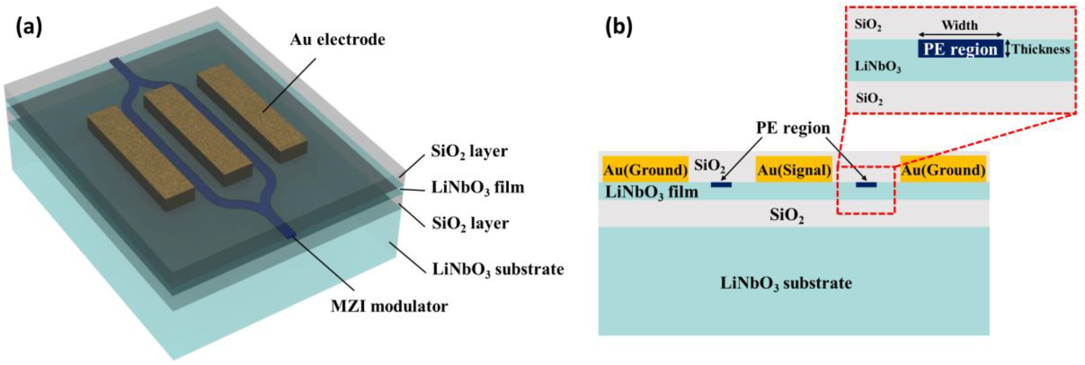
2. Device Design and Methods

The material of the device studied was an x-cut LN thin film bonded to a SiO2 layer deposited on an LN-substrate [17]. The thicknesses of the LN thin film and the SiO2 layer were 0.5 μm and 2 μm [30], respectively. The structures were cladded with 2-μm-thick SiO2 layers after the PE waveguides and electrodes were fabricated. Figure 1a shows a schematic of the M-ZI. The input wave was emitted into a directional coupler. The input power was divided equally into the two output waveguides with a first directional coupler. The two waveguides formed the two arms of the M-ZI. On both arms, opposite electric fields were applied to modify the refractive of the LN and thus change the phase of the wave propagating through that arm. The two waves were then combined into another 50/50 directional coupler. By varying the applied voltage, the amount of light emitted from the two output waveguides could be continuously controlled.
Figure 1b shows the schematic cross-sections of the M-ZI and the channel waveguide. The lateral diffusion could be neglected when the thickness of the PE was much lower than the mask width, and a rectangular step-like refractive index profile could be formed during the PE process, as shown in the inset of Figure 1b. The PE region formed stripe-loaded channel waveguides, and the LN thin film on both sides of the PE region formed planar waveguides. The PE only increased the extraordinary refractive index (ne) of the LN crystal and it therefore supported only one type of mode in the channel waveguides (the transverse electric (TE) mode in the x-cut LNOI). The ordinary and extraordinary refractive index changes were −0.05 and 0.08, respectively. Table 1 shows the refractive indices of the material at the wavelength of 1.55 μm. In previous studies on bulk LN, the PE waveguides generally suffered from a dramatically reduced E-O coefficient for the electro-optic devices [31]. Since the E-O coefficient of the unannealed proton exchange region was close to zero, it was set to zero in the simulation.
The full-vectorial finite difference method was regarded as a simple and effective method to solve the bending loss and the mode distribution. The finite difference algorithm was used to mesh the geometry of the waveguide. This algorithm had the ability to adapt to the arbitrary waveguide structure. After the structure was meshed, Maxwell’s equations were then transformed into matrix eigenvalue problems and solved by sparse matrix techniques to obtain the effective indices and the mode distribution of the waveguide modes [33]. The FD-BPM was employed to simulate the M-ZI. The method consisted of marching the input optical field over small distances in the dielectric media with the use of a fast Fourier transform. In each propagational step, the plane spectrum was used to simulate the optical field in the spectral domain, and due to the medium inhomogeneity, a phase correction was introduced in the spatial domain [34].

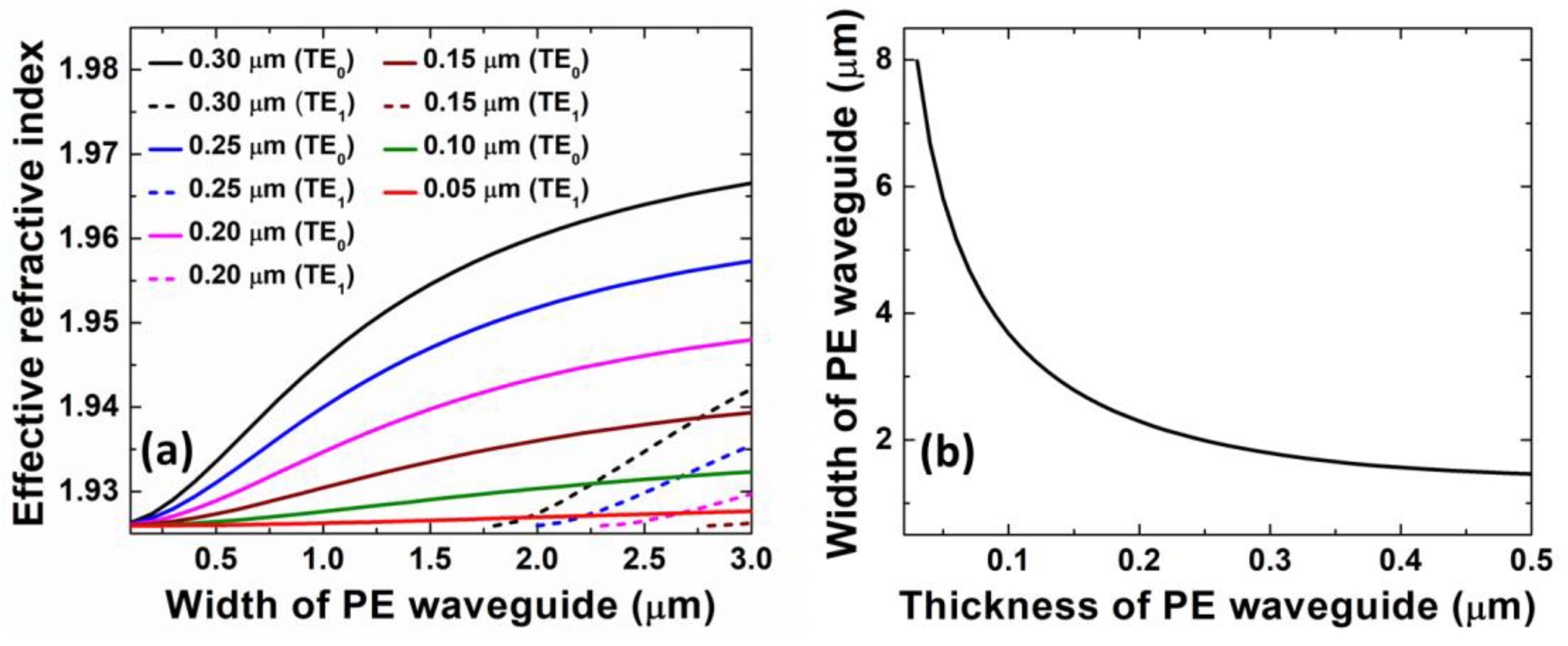
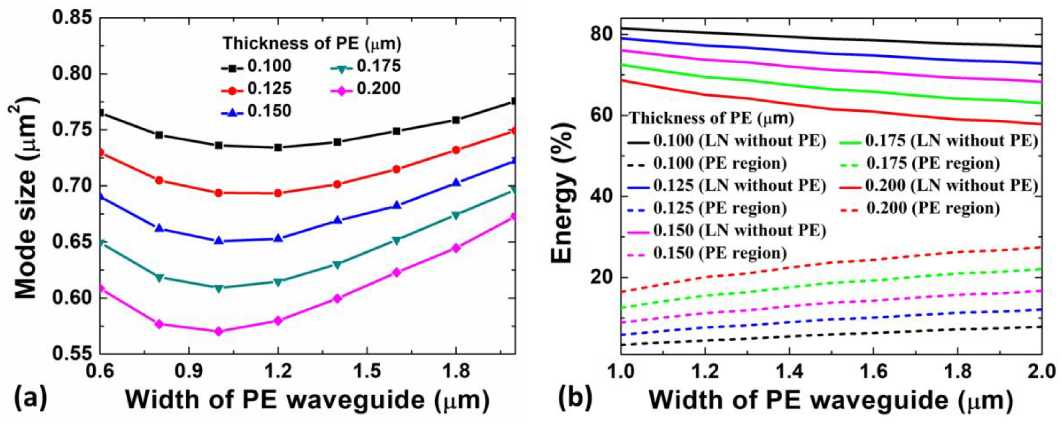
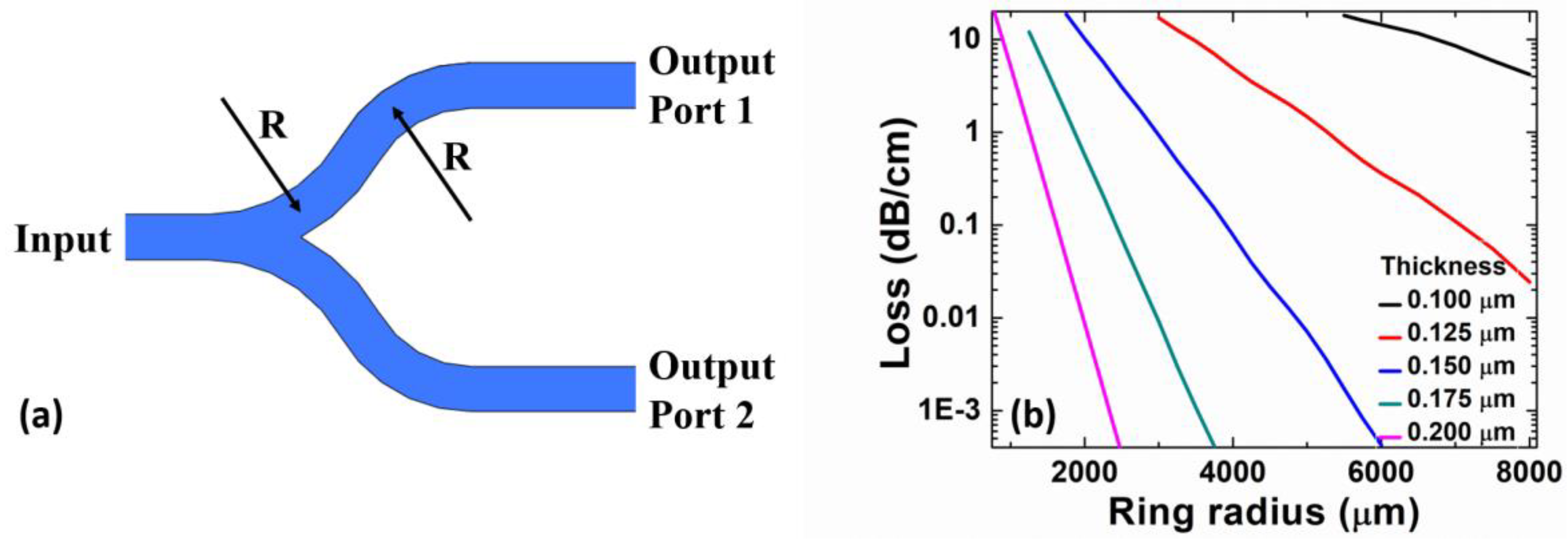
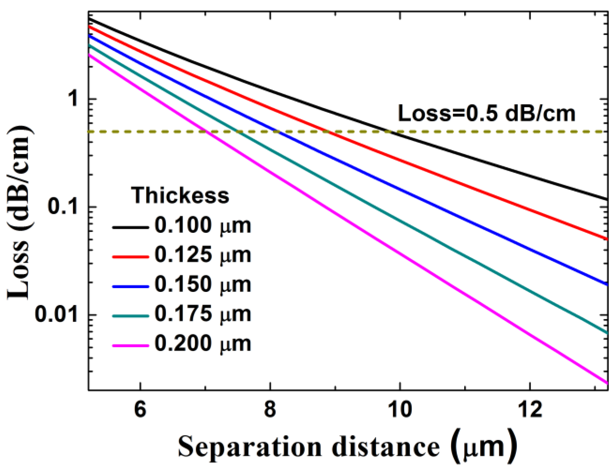
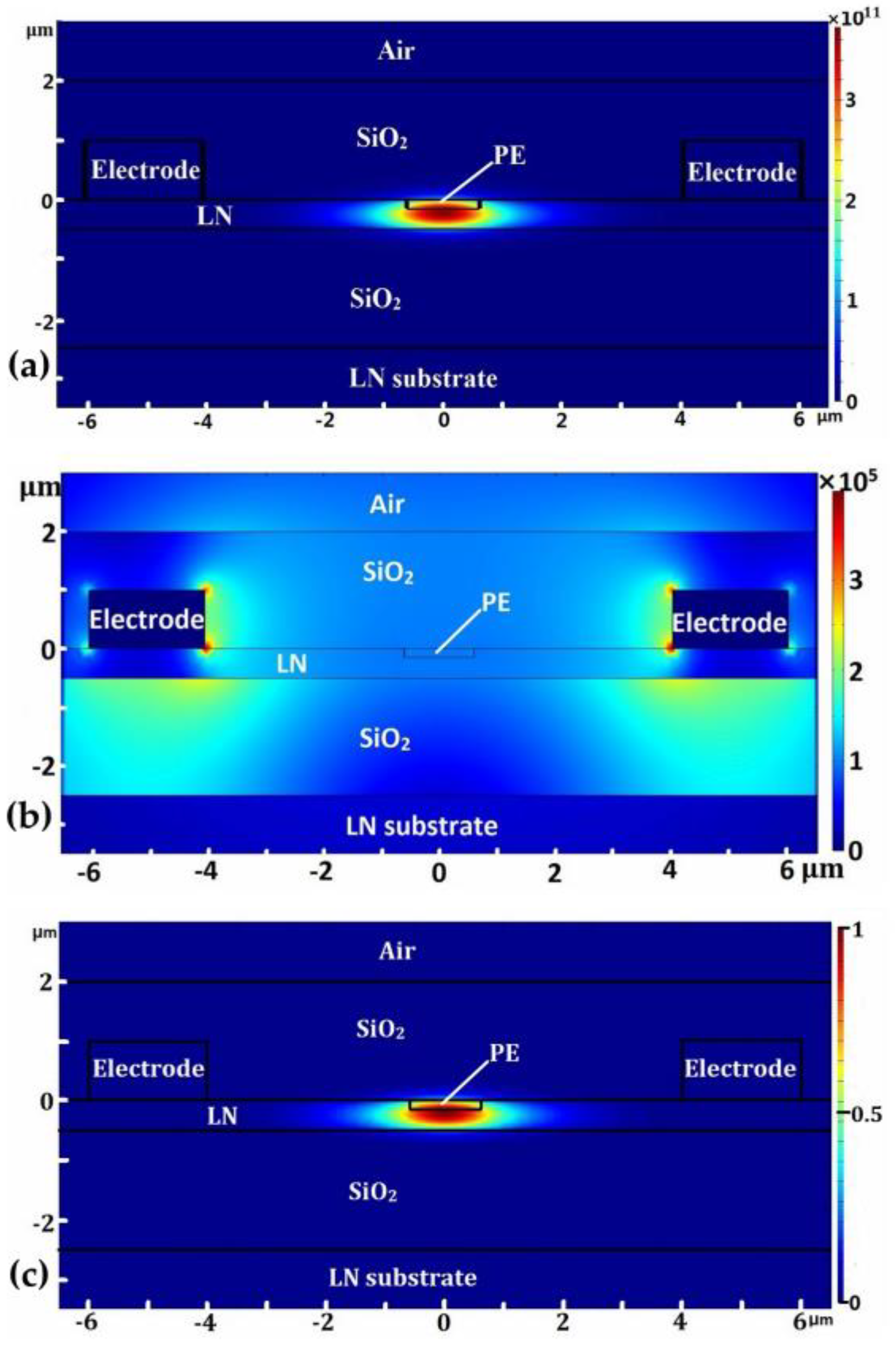
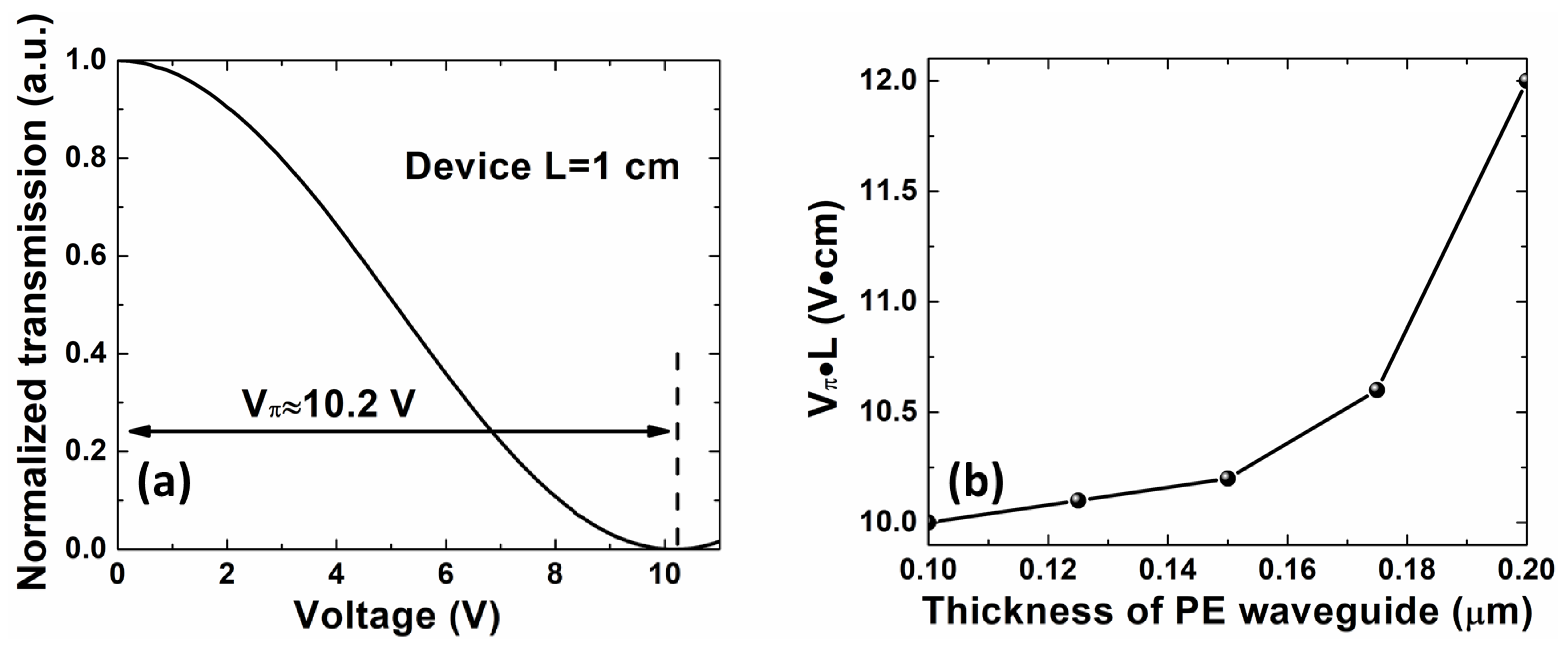
3. Results and Discussion

The single-mode conditions were simulated to prevent the distortion of the signal during transmission. We calculated the modal curves of the PE waveguides at a wavelength of λ = 1.55 μm. The effective indices of the TE mode in the PE waveguides as a function of the width for different thicknesses of the PE region are presented in Figure 2a. As the width and thickness of the PE waveguides decreased, the effective refractive index decreased, and the more high-order modes disappeared. The TE0 modes represented the fundamental TE modes. The cutoff dimension of the PE waveguide for the TE mode between the single- and multi-mode conditions was calculated, as shown in Figure 2b. Any dimensions beneath the curves fulfilled the single-mode condition. As the cut-off width increased, the PE thickness decreased.
A small mode size enabled the development of ultra-compact PICs and strengthened the E-O effect. For the channel waveguide in the LNOI, due to the large refractive index contrast between the LN layer and the SiO2 cladding, the light was strongly confined, resulting in a smaller mode size. Figure 3a shows the simulation results of the relationship between the mode size (the 1/e intensity in the vertical and horizontal directions formed the two axes of the ellipse) and the width and thickness of the PE waveguides. The mode size decreased with the increasing PE thickness. When the width initially increased, the confinement of the light became strong, which also led to a smaller mode size. As the waveguide width increased further, the PE region expanded and the mode size became larger. The shape of the smallest mode size decreased in width as the thickness increased. For the composite strip waveguide, the optical power was mainly divided into three parts. The first part was in the PE region, the second part was in the LN layer without PE, and the third part was in the SiO2 cladding layer. The E-O effect ascended with the increasing optical power in the LN layer without PE. This required most of the optical power to be concentrated in the LN layer without PE. Figure 3b shows the optical powers in the LN layer without PE and the PE region for the TE modes. The optical power in the LN layer without PE increased slightly with the shrinking of the PE width and thickness. Therefore, the width and thickness of the PE strip had a certain influence on the optical power distribution. Considering the single-mode conditions, mode sizes, and optical power distribution, the widths of the PE waveguides were all selected as 1.2 µm in the following simulations.
Figure 4a shows the schematic of the Y-branch. It consisted of two symmetrical arms between one input and two output straight waveguides. Each arm consisted of two identical circular arcs of radius R which had the same width as the input and output waveguides. Since the structure involved a bend waveguide (circular arcs on each arm), the relationship between the bending loss and the bending radius was as shown in Figure 4b. The bending loss increased sharply with the decreasing bending radius and thickness of the PE region.
To obtain the maximum electric field, an appropriate separation distance between the electrodes had to be selected. The separation distances were dictated by the propagation losses introduced by the electrodes near the PE waveguides. The propagation losses with different separation distances between the electrodes at a wavelength of λ = 1.55 μm are shown in Figure 5. The propagation loss increased sharply with the diminishing separation distance. In the following simulation, the separation distance between the electrodes was selected to have a PE waveguide loss of approximately 0.5 dB/cm. For radio frequency (RF) attenuation, thick metals facilitate low-loss RF waveguides. When the electrode thickness was larger than 1 μm, the decrease of the RF attenuation was saturated [12]. To achieve the optimum performance of the electro-optic modulator, the thickness of the electrodes could be selected as 1 µm.
As shown in Figure 6a,b, the optical field and the electrostatic field were simulated. Figure 6c shows the overlap integral of the optical and electrostatic fields. The PE waveguide had a thickness of 0.15 µm and a width of 1.2 µm, allowing confinement for most of the optical power in the LN core without PE, which was the E-O active material. We could design electrodes to be placed close to the waveguides without substantially bigger optical transmission losses.
To control the optical properties with an external electric signal, the E-O effect or the Pockels effect was used, where the birefringence of the crystal changed proportionally to the applied electric field. A change in the refractive index resulted in a change of the phase of the wave passing through the crystal. If two waves with different phase change were combined, the amplitude modulation could be performed by an interferometer. An important quality factor for the M-ZI modulators was the half-wave voltage (Vπ), defined as the required voltage to induce a π-phase difference between the two modulator arms, changing the optical transmission from the maximum to minimum. Figure 7a shows the optical transmission of a device with 1-cm-long microwave strip line electrodes, for which we calculated a low Vπ of 10.2 V (the thickness and the width of PE waveguide and the separation distance between electrodes were 0.15, 1.2, and 8.08 µm, respectively). Figure 7b shows that the half-wave voltage length product varied with the thickness of the PE region. The half-wave voltage length product ascended with the increasing thickness of the PE waveguide. Considering the bending loss of the Y branch and the half-wave voltage length product, the most suitable thickness of the PE waveguide was 0.15 µm.
The frequency-dependent refractive index mismatch between the optical and RF signals played a key role in the final modulation bandwidth of the modulator [1]. Thanks to the LN thin film structure, the refractive index of the RF and optical modes was well matched in the modulator [12]. This was different to the ordinary bulk LN modulators [35]. By further adjusting the structural parameters of the waveguides and electrodes, the mismatch refractive index between the optical and RF signals should be minimized as much as possible, which should be studied carefully in the future.

4. Conclusions

The full-vectorial finite-difference method was used to calculate the single-mode conditions, mode sizes, and optical power distribution of the PE channel waveguides. The widths of the PE waveguides were optimized to 1.2 µm. The propagation losses of the guided mode at different separation distances between the electrodes were analyzed and discussed. As a very important aspect of the practical application, the half-wave voltages were simulated using FD-BPM. The thickness of the PE waveguides and the separation distances between the electrodes were optimized to 0.15 µm and 8.08 µm, respectively. The optimized value of Vπ·L was calculated to be 10.2 V·cm.

Author Contributions

B.X. conceived the original idea; H.H. carried out the simulations and wrote the manuscript; H.H., B.X., T.L., G.C. and S.R. contributed the useful and deep discussions, analyzed the data and modified the manuscript.

Funding

This work was supported by the Shenzhen Science and Technology Planning (NO. JCYJ20170818143327496), the Project of Youth Innovative Talents in Higher Education Institutions of Guangdong (NO. 2018KQNCX399), the Foundation of Zibo Vocational Institute (NO. 2018zzzr03), the School City Integration Development Plan of Zibo (NO. 2019ZBXC127), and the Shandong University Science and Technology Planning (NO. J16LN93).

Conflicts of Interest

The authors declare no conflict of interest.

References

  1. Honardoost, A.; Safian, R.; Rao, A.; Fathpour, S. High-Speed Modeling of Ultracompact Electrooptic Modulators. J. Light. Technol. 2018, 36, 5893–5902. [Google Scholar] [CrossRef]
  2. Janner, D.; Tulli, D.; García-Granda, M.; Belmonte, M.; Pruneri, V. Micro-structured integrated electro-optic LiNbO3 modulators. Laser Photonics Rev. 2019, 3, 301–313. [Google Scholar] [CrossRef]
  3. Chuang, R.W.; Hsu, M.T.; Chang, Y.C.; Lee, Y.J.; Chou, S.H. Integrated multimode interference coupler-based Mach–Zehnder interferometric modulator fabricated on a silicon-on-insulator substrate. IET Optoelectron. 2012, 6, 147–152. [Google Scholar] [CrossRef]
  4. Chen, H.W.; Kuo, Y.H.; Bowers, J.E. High speed hybrid silicon evanescent Mach-Zehnder modulator and switch. Opt. Express 2008, 16, 20571–20576. [Google Scholar] [CrossRef] [PubMed]
  5. Ding, J.; Shao, S.; Zhang, L.; Fu, X.; Yang, L. Method to improve the linearity of the silicon Mach-Zehnder optical modulator by doping control. Opt. Express 2016, 24, 24641–24648. [Google Scholar] [CrossRef]
  6. Kitoh, T. Recent progress on arrayed-waveguide grating multi/demultiplexers based on silica planar lightwave circuits. Proc. SPIE 2008, 7135, 713503. [Google Scholar]
  7. Maru, K.; Mizumoto, M.; Uetsuka, H. Demonstration of Flat-Passband Multi/Demultiplexer Using Multi-Input Arrayed Waveguide Grating Combined with Cascaded Mach-Zehnder Interferometers. J. Light. Technol. 2007, 25, 2187–2197. [Google Scholar] [CrossRef]
  8. Cahill, L.W. The modelling of integrated optical power splitters and switches based on generalised Mach-Zehnder devices. Opt. Quantum Electron. 2004, 36, 165–173. [Google Scholar] [CrossRef]
  9. Cherchi, M. Design scheme for Mach–Zehnder interferometric coarse wavelength division multiplexing splitters and combiners. J. Opt. Soc. Am. B 2006, 23, 1752–1756. [Google Scholar] [CrossRef]
  10. Weis, R.S.; Gaylord, T.K. Lithium niobate: Summary of physical properties and crystal structure. Appl. Phys. A 1985, 37, 191–203. [Google Scholar] [CrossRef]
  11. Wang, C.; Zhang, M.; Chen, X.; Bertrand, M.; Shams-Ansari, A.; Chandrasekhar, S.; Winzer, P.; Lončar, M. Integrated lithium niobate electro-optic modulators operating at CMOS-compatible voltages. Nature 2018, 562, 101–104. [Google Scholar] [CrossRef] [PubMed]
  12. He, M.; Xu, M.; Ren, Y.; Jian, J.; Ruan, Z.; Xu, Y.; Gao, S.; Sun, S.; Wen, X.; Zhou, L.; et al. High-performance hybrid silicon and lithium niobate Mach–Zehnder modulators for 100 Gbit s−1 and beyond. Nat. Photonics 2019, 13, 359–364. [Google Scholar] [CrossRef]
  13. Weigel, P.O.; Zhao, J.; Fang, K.; Al-Rubaye, H.; Trotter, D.; Hood, D.; Mudrick, J.; Dallo, C.; Pomerene, A.T.; Starbuck, A.L.; et al. Bonded thin film lithium niobate modulator on a silicon photonics platform exceeding 100 GHz 3-dB electrical modulation bandwidth. Opt. Express 2018, 26, 23728–23739. [Google Scholar] [CrossRef] [PubMed] [Green Version]
  14. Mercante, A.J.; Shi, S.; Yao, P.; Xie, L.; Weikle, R.M.; Prather, D.W. Thin film lithium niobate electro-optic modulator with terahertz operating bandwidth. Opt. Express 2018, 26, 14810–14816. [Google Scholar] [CrossRef]
  15. Rao, A.; Patil, A.; Rabiei, P.; Honardoost, A.; Desalvo, R.; Paolella, A.; Fathpour, S. High-performance and linear thin-film lithium niobate Mach–Zehnder modulators on silicon up to 50 GHz. Opt. Lett. 2016, 41, 5700–5703. [Google Scholar] [CrossRef]
  16. Poberaj, G.; Hu, H.; Sohler, W.; Günter, P. Lithium niobate on insulator (LNOI) for micro-photonic devices. Laser Photonics Rev. 2012, 6, 488–503. [Google Scholar] [CrossRef]
  17. Han, H.; Cai, L.; Hu, H. Optical and structural properties of single-crystal lithium niobate thin film. Opt. Mater. 2015, 42, 47–51. [Google Scholar] [CrossRef]
  18. Xiang, B.; Guan, J.; Jiao, Y.; Wang, L. Fabrication of ion-sliced lithium niobate slabs using helium ion implantation and Cu–Sn bonding. Phys. Status Solidi (A) 2014, 211, 2416–2420. [Google Scholar] [CrossRef]
  19. Hu, H.; Ricken, R.; Sohler, W. Lithium niobate photonic wires. Opt. Express 2009, 17, 24261–24268. [Google Scholar] [CrossRef]
  20. Zhang, M.; Wang, C.; Cheng, R.; Shams-Ansari, A.; Lončar, M. Monolithic ultra-high-Q lithium niobate microring resonator. Optica 2017, 4, 1536–1537. [Google Scholar] [CrossRef]
  21. Honardoost, A.; Juneghani, F.A.; Safian, R.; Fathpour, S. Towards subterahertz bandwidth ultracompact lithium niobate electrooptic modulators. Opt. Express 2019, 27, 6495–6501. [Google Scholar] [CrossRef] [PubMed]
  22. Cai, L.; Mahmoud, A.; Piazza, G. Low-loss waveguides on Y-cut thin film lithium niobate: Towards acousto-optic applications. Opt. Express 2019, 27, 9794–9802. [Google Scholar] [CrossRef] [PubMed]
  23. Cai, L.; Kong, R.; Wang, Y.; Hu, H. Channel waveguides and y-junctions in x-cut single-crystal lithium niobate thin film. Opt. Express 2015, 23, 29211–29221. [Google Scholar] [CrossRef] [PubMed]
  24. Wu, R.; Wang, M.; Xu, J.; Qi, J.; Chu, W.; Fang, Z.; Zhang, J.; Zhou, J.; Qiao, L.; Chai, Z.; et al. Long Low-Loss-Litium Niobate on Insulator Waveguides with Sub-Nanometer Surface Roughness. Nanomaterials 2018, 8, 910. [Google Scholar] [CrossRef] [PubMed]
  25. Ganshin, V.A.; Korkishko, Y.N. Proton exchange in lithium niobate and lithium tantalate single crystals: Regularities and specific features. Phys. Status Solidi (A) 1990, 119, 11–25. [Google Scholar] [CrossRef]
  26. Canali, C.; Carnera, A.; Mea, G.D.; Mazzoldi, P.; Shukri, S.M.A.; Nutt, A.C.G.; Rue, R.M.D.L. Structural characterization of proton exchanged LiNbO3 optical waveguides. J. Appl. Phys. 1986, 59, 2643–2649. [Google Scholar] [CrossRef]
  27. Xu, C.L.; Huang, W.P.; Stern, M.S.; Chaudhuri, S.K. Full-vectorial mode calculations by finite difference method. IEE Proc. Optoelectron. 1994, 141, 281–286. [Google Scholar] [CrossRef]
  28. Scarmozzino, R.; Gopinath, A.; Pregla, R.; Helfert, S. Numerical techniques for modeling guided-wave photonic devices. IEEE J. Sel. Top. Quantum Electron. 2000, 6, 150–162. [Google Scholar] [CrossRef]
  29. Scarmozzino, R.; Osgood, R.M. Comparison of finite-difference and Fourier-transform solutions of the parabolic wave equation with emphasis on integrated-optics applications. J. Opt. Soc. Am. A 1991, 8, 724–731. [Google Scholar] [CrossRef]
  30. Han, H.; Xiang, B.; Zhang, J. Simulation and analysis of single-mode microring resonators in lithium niobate thin film. Crystals 2018, 8, 342. [Google Scholar] [CrossRef]
  31. Méndez, A.; Paliza, G.D.L.; Garcia-Cabanes, A.; Cabrera, J.M. Comparison of the electro-optic coefficient r33 in well-defined phases of proton exchanged LiNbO3 waveguides. Appl. Phys. B 2001, 73, 485–488. [Google Scholar] [CrossRef]
  32. Schlarb, U.; Betzler, K. A generalized sellmeier equation for the refractive indices of lithium niobate. Ferroelectrics 1994, 156, 99–104. [Google Scholar] [CrossRef]
  33. Lumerical Solutions. Available online: http://www.lumerical.com/ (accessed on 25 August 2019).
  34. Chung, Y.; Dagli, N. An assessment of finite difference beam propagation method. IEEE J. Quantum Electron. 1990, 26, 1335–1339. [Google Scholar] [CrossRef]
  35. Wooten, E.; Kissa, K.; Yi-Yan, A.; Murphy, E.; Lafaw, D.; Hallemeier, P.; Maack, D.; Attanasio, D.; Fritz, D.; McBrien, G.; et al. A review of lithium niobate modulators for fiber-optic communications systems. IEEE J. Quantum Electron. 2000, 6, 69–82. [Google Scholar] [CrossRef]
Figure 1. (a) Schematic of the M-ZI. (b) The cross-sectional schematic of the M-ZI and the channel waveguides.
Crystals 09 00549 g001
Figure 2. (a) Effective indices of the transverse electric (TE) modes in the proton exchange (PE) waveguides as a function of the width for different thicknesses of the PE waveguides. (b) Cut-off dimensions of the PE region for the TE mode.
Crystals 09 00549 g002
Figure 3. (a) Relationship between the mode size and the width and thickness of the PE waveguide. (b) Relationship between the optical power and the width and thickness of the PE waveguide.
Crystals 09 00549 g003
Figure 4. (a) Schematic of the symmetrical Y-Branch. (b) The dependence of the bending loss on the bending radius of the channel waveguide with a 1.2 μm width, using the thickness of the PE waveguide as the parameter.
Crystals 09 00549 g004
Figure 5. Relationship between the propagation loss and the separation distance.
Crystals 09 00549 g005
Figure 6. (a) Optical field inside the waveguide. (b) Electrostatic field after a 1 V voltage was applied to the electrodes. (c) Normalized product of the optical and electrical fields.
Crystals 09 00549 g006
Figure 7. (a) Normalized optical transmission of a 1-cm device as a function of the applied voltage. (b) Half-wave voltage-length product variation with the thickness of the PE waveguide.
Crystals 09 00549 g007
Table 1. Refractive indices of the material in simulation (λ = 1.55 μm).
Materialnone
LN [32]2.2112.138
PE [23]2.1612.218
SiO21.461.46

