Subthreshold Characteristics of a Metal-Oxide–Semiconductor Field-Effect Transistor with External PVDF Gate Capacitance


1
Department of Applied Materials and Optoelectronic Engineering, National Chi Nan University, Nantou, Puli 54561, Taiwan
2
Department of Electrical Engineering, National Chi Nan University, Nantou, Puli 54561, Taiwan
*
Author to whom correspondence should be addressed.
Crystals 2019, 9(12), 673; https://0-doi-org.brum.beds.ac.uk/10.3390/cryst9120673
Submission received: 28 November 2019
/
Revised: 6 December 2019
/
Accepted: 11 December 2019
/
Published: 14 December 2019
(This article belongs to the Special Issue Selected Papers from Taiwan Association for Academic Innovation, TAAI 2019)
Abstract
:An organic ferroelectric capacitor, using polyvinylidene difluoride (PVDF) as the dielectric, was fabricated. By connecting the PVDF capacitor in series to the gate of a commercially purchased metal-oxide–semiconductor field-effect transistor (MOSFET), drain current (ID)–drain voltage (VD) characteristics and drain current (ID)–gate voltage (VG) characteristics were measured. In addition, the subthreshold slopes of the MOSFET were determined from the ID–VG curves. It was found that the subthreshold slope could be effectively reduced by 23% of its original value when the PVDF capacitor was added to the gate of the MOSFET.
1. Introduction
When under a subthreshold condition, modern metal-oxide–semiconductor field-effect transistors (MOSFETs) face a fundamental limit, termed the Boltzmann tyranny, which is a direct result of the Boltzmann distribution of electrons at the source/channel interface. Consequently, a gate-source voltage of at least 60 mV/decade at room temperature is required to switch the transistor between ON state and OFF state [1,2]. This subthreshold slope (SS) limit restricts the power consumption of MOSFETs from being reduced any further [2]. As portable electronic devices are gradually becoming indispensable in our daily life, it is crucial to overcome this power consumption barrier, that is, to reduce the SS. Therefore, determining precisely how to remove the Boltzmann tyranny has recently constituted a popular topic of research [3,4,5,6,7,8,9,10]. At least two different approaches have been proposed: (1) to use the tunnel junction at the source/channel end of the MOSFET (called the tunnel field-effect transistor or tunnel FET) [11,12,13,14]; and (2) to use the negative gate capacitance of the MOSFET. Negative capacitance has been observed in many different materials and device structures including ferroelastic switches, oxidesuperlattices, supercrystals, and light-emitting diodes [15,16,17,18,19,20,21]. It can be practically achieved by utilizing ferroelectric dielectric materials such as AlInN [8], BiFeO3 [9], and HfZrO2 [14], due to the lag of the polarization charge inside the ferroelectric materials with respect to the change of applied voltage. It has also been reported that connecting a negative capacitance externally in series with the gate of the MOSFET can effectively alleviate this 60 mV/decade SS constraint [6,9,22]. It is important to note that some organic materials also possess ferroelectricity. Among them, however, only polyvinylidene fluoride trifluorethylene [P(VDF-TrFE)], and no other organic ferroelectric material, has been identified in the literature for the SS reduction of MOSFETs [9,10,23]. Since PVDF itself constitutes an organic ferroelectric material and is easily accessible, we attempted to fabricate a capacitor with PVDF as the dielectric material and tested its effect on the SS characteristics of MOSFETs. Since negative capacitance is challenging to measure directly using conventional measurement techniques, we externally connected the PVDF capacitor in series with the gate of the MOSFET and determined its subthreshold characteristics.
2. Materials and Methods
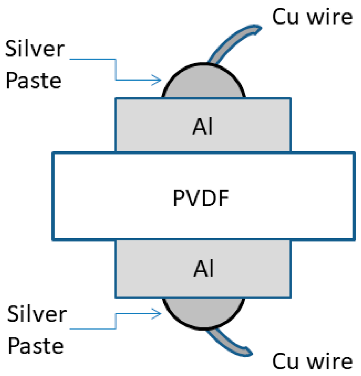
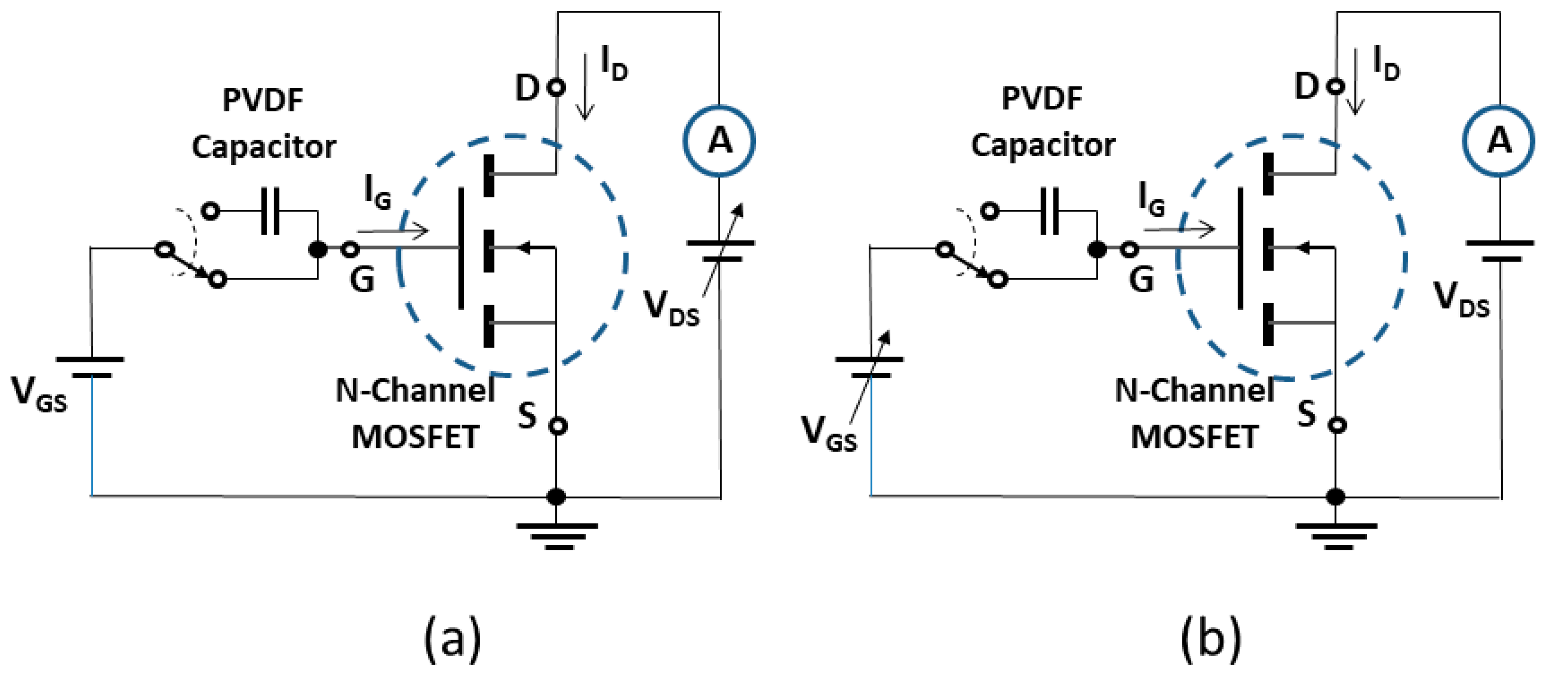
PVDF capacitors with a metal–dielectric–metal structure were fabricated. A high-quality PVDF film with a thickness of 1 μm was purchased directly from the vendor (Dongguan Haozheng Trading Co. Ltd., Dongguan, China) and aluminum (Al) films were deposited on both sides of the PVDF films through a metal mask to form the top and bottom electrodes. The area of the top electrode was approximately 100 mm2, and the electrode area was controlled by the metal mask. Copper wires were then attached to both electrodes using conductive silver paste. Figure 1 shows the device structure of the PVDF capacitor used in this work. The MOSFETs (HCF4007UBE, STMicroelectronics, Inc. Geneva, Switzerland) used in this work were purchased and used without modification. The ID–VD and subthreshold ID–VG characteristics of the n-channel MOSFETs, with and without PVDF capacitors connected in series with the gate, were measured by an Agilent 4156B semiconductor parameter analyzer (Agilent Technologies (Taiwan), Taipei, Taiwan). The subthreshold slopes of the MOSFETs were then identified from the subthreshold ID–VG characteristics. Figure 2a,b illustrate, respectively, the measurement circuits for ID–VD and ID–VG characteristics with and without connection of the PVDF capacitor.
3. Results and Discussion
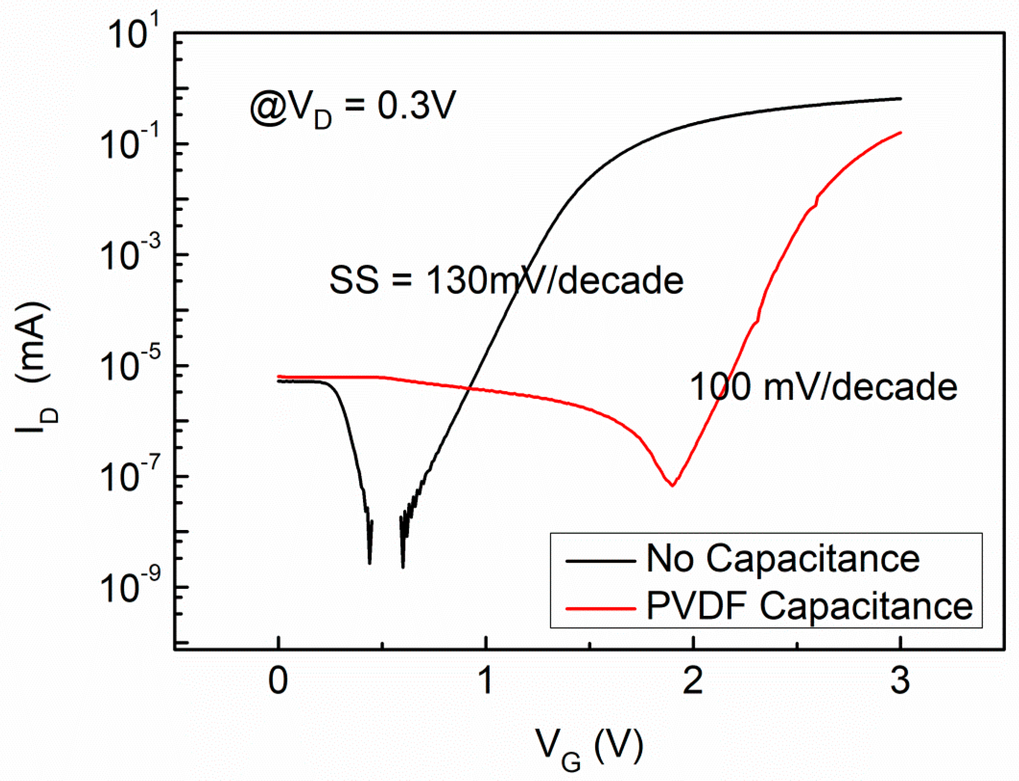
Figure 3a presents the ID–VD curves of the n-channel MOSFET (HCF4007UBE, STMicroelectronics, Inc.) without connecting a PVDF capacitor at the gate, under VG = 1, 2, and 3 V, respectively. Since the HCF4007UBE MOSFET was originally designed for digital circuit applications, the IDs between different VGs are not evenly spaced. Figure 3b depicts the ID–VD curves of the n-channel MOSFET (HCF4007UBE) with a PVDF capacitor connected at the gate under VG = 1, 2, and 3 V, respectively. By comparing the ID–VD curves shown in Figure 3a,b, it can be seen that the drain current ID was apparently lower after the transistor connected a PVDF capacitor in series with the gate. This is because an additional voltage drop across the PVDF capacitor made the effective gate voltage VG smaller. In addition, a sunken current in IDs was observed when the MOSFET was connected with a PVDF capacitor, as shown in Figure 3b. This sunken drain current behavior indicates that the charges in the channel of the MOSFET were reduced when the gate voltage VG increased, implying an effective negative gate capacitance. To further examine the negative capacitance effect of the PVDF capacitor, we measured the ID–VG characteristics of the MOSFET connected or not to a PVDF capacitor at the gate of the transistor and then compared their subthreshold slopes. Figure 4 compares the ID–VG characteristics of the MOSFET connected or not to a PVDF capacitor at the gate of the transistor for VD = 0.3 V, in which the subthreshold slope of each ID–VG characteristic is specified. It was found that the subthreshold slope for the original HCF4007UBE MOSFET was SS = 130 mV/decade, while the SS for the transistor connected with a PVDF capacitor was SS = 100 mV/decade.
4. Conclusions
The extant literature has not yet addressed the negative capacitance of PVDF, even though it is an organic ferroelectric material. In this work, we investigated the effect of connecting an organic PVDF capacitor in series with the gate of an n-channel MOSFET. A sunken drain current behavior was found in the ID–VD curves of the transistor when it was connected with a PVDF capacitor at its gate, indicating the existence of an effective negative gate capacitance. It was also found that the subthreshold slope of the transistor decreased from 130 mV/decade to 100 mV/decade, which constitutes a reduction of 23% of its original value. This result confirms the negative capacitance effect of the PVDF and proves that connecting a PVDF capacitor in series to the gate of a MOSFET can effectively decrease the subthreshold slope of the transistor. Although the MOSFET used in this work was not a state-of-the-art one and had a high SS, it is believed that by connecting a PVDF capacitor in series to the gate, the SS could be reduced to below 60mV/decade if a scaled MOSFET was used instead.
Author Contributions
Conceptualization, J.-J.L. and Y.-L.W.; methodology, J.-J.L..; formal analysis, J.-H.T.; resources, Y.-L.W.; data curation, J.-J.L. and J.-H.T.; writing—original draft preparation, Y.-L.W.; visualization, Y.-L.W.; experimentation, J.-H.T.
Funding
This research was funded by the Ministry of Science and Technology, Taiwan, R.O.C. under contract no. MOST 107-2221-E-260-013.
Conflicts of Interest
The authors declare no conflict of interest.
References
- Zhirnov, V.V.; Cavin, R.K. Negative capacitance to the rescue? Nat. Nanotechnol. 2008, 3, 77–78. [Google Scholar] [CrossRef]
- Theis, T.N.; Solomon, P.M. It’s time to reinvent transistor. Science 2010, 327, 1600–1601. [Google Scholar] [CrossRef]
- Han, G.; Zhou, J.; Liu, Y.; Li, J.; Peng, Y.; Hao, Y. Experimental investigation of fundamentals of negative capacitance FETs. In Proceedings of the 2018 IEEE SOI-3D-Subthreshold Microelectronics Technology Unified Conference (S3S), Burlingame, CA, USA, 15–18 October 2018; pp. 1–2. [Google Scholar]
- Krivokapic, Z.; Rana, U.; Galatage, R.; Razavieh, A.; Aziz, A.; Liu, J.; Shi, J.; Kim, H.J.; Sporer, R.; Serrao, C.; et al. 14 nm ferroelectric FinFET technology with steep subthreshold slope for ultra-low power applications. In Proceedings of the IEEE International Electron Devices Meeting (IEDM), San Francisco, CA, USA, 2–6 December 2017; pp. 15.1.1–15.1.4. [Google Scholar]
- Khan, A.I.; Chatterjee, K.; Wang, B.; Drapcho, S.; You, L.; Serrao, C.; Bakaul, S.R.; Ramesh, R.; Salahuddin, S. Negative capacitance in a ferroelectric capacitor. Nat. Mater. 2015, 14, 182–186. [Google Scholar] [CrossRef] [PubMed]
- Jo, J.; Choi, W.Y.; Park, J.-D.; Shim, J.W.; Yu, H.-Y.; Shin, C. Negative capacitance in organic/ferroelectric capacitor to implement steep switching MOS devices. Nano Lett. 2015, 15, 4553–4556. [Google Scholar] [CrossRef] [PubMed]
- Ku, H.; Shin, A. Transient response of negative capacitance in P(VDF0.75-TrFE0.25) organic ferroelectric capacitor. IEEE J. Electron Devices Soc. 2017, 5, 232–236. [Google Scholar] [CrossRef]
- Then, H.W.; Dasgupta, S.; Radosavljevic, M.; Chow, L.; Chu-Kung, B.; Dewey, G.; Gardner, S.; Gao, X.; Kavalieros, J.; Mukherjee, N.; et al. Experimental observation and physics of “negative” capacitance and steeper than 40mV/decade subthreshold swing in Al0.83In0.17N/AlN/GaN MOS-HEMT on SiC substrate”. In Proceedings of the IEEE International Electron Devices Meeting, Washington, DC, USA, 9–11 December 2013; pp. 28.3.1–28.3.4. [Google Scholar]
- Khan, A.I.; Chatterjee, K.; Duarte, J.P.; Lu, Z.; Sachid, A.; Khandelwal, S.; Ramesh, R.; Hu, C.; Salahuddin, S. Negative capacitance in short-channel FinFETs externally connected to an epitaxial ferroelectric capacitor. IEEE Elect. Dev. Lett. 2016, 37, 111–114. [Google Scholar] [CrossRef]
- Salvatore, G.A.; Bouvet, D.; Ionescu, A.M. Demonstration of subthreshold swing smaller than 60mV/decade in Fe-FET with P(VDF-TrFE)/SiO2gate stack. In Proceedings of the International Electron Devices Meeting, San Francisco, CA, USA, 15–17 December 2008; pp. 1–4. [Google Scholar]
- Choi, W.Y.; Park, B.-G.; Lee, J.D.; Liu, T.-J.K. Tunneling field-effect transistors (TFETs) with subthreshold swing (SS) less than 60 mV/dec. IEEE Electron Device Lett. 2007, 28, 743–745. [Google Scholar] [CrossRef]
- Khatami, Y.; Banerjee, K. Steep subthreshold slope n- and p-type tunnel-FET devices for low-power and energy-efficient digital circuits. IEEE Trans. Elect. Dev. 2009, 56, 2752–2761. [Google Scholar] [CrossRef]
- Liu, H.; Datta, S.; Narayanan, V. Steep switching tunnel FET: A promise to extend the energy efficient roadmap for post-CMOS digital and analog/RF applications. In Proceedings of the International Symposium on Low Power Electronics and Design (ISLPED), Beijing, China, 4–6 September 2013; pp. 145–150. [Google Scholar]
- Li, K.S.; Chen, P.G.; Lai, T.Y.; Lin, C.H.; Cheng, C.C.; Chen, C.C.; Wei, Y.J.; Hou, Y.F.; Liao, M.H.; Lee, M.H.; et al. Sub-60mV-swing negative-capacitance FinFET without hysteresis. In Proceedings of the IEEE International Electron Devices Meeting (IEDM), Washington, DC, USA, 7–9 December 2015; pp. 22.6.1–22.6.4. [Google Scholar]
- Yadav, A.K.; Nguyen, K.X.; Hong, Z.; García-Fernández, P.; Aguado-Puente, P.; Nelson, C.T.; Das, S.; Prasad, B.; Kwon, D.; Cheema, S.; et al. Spatially resolved steady-state negative capacitance. Nature 2019, 565, 468–471. [Google Scholar] [CrossRef] [PubMed] [Green Version]
- Das, S.; Tang, Y.L.; Hong, Z.; Gonçalves, M.A.P.; McCarter, M.R.; Klewe, C.; Nguyen, K.X.; Gómez-Ortiz, F.; Shafer, P.; Arenholz, E.; et al. Observation of room-temperature polar skyrmions. Nature 2019, 568, 368–372. [Google Scholar] [CrossRef] [PubMed] [Green Version]
- Lu, X.; Chen, Z.; Cao, Y.; Tang, Y.; Xu, R.; Saremi, S.; Zhang, Z.; You, L.; Dong, Y.; Das, S.; et al. Mechanical-force-induced non-local collective ferroelastic swiching in epitaxial lead-titanate thin films. Nat. Commun. 2019, 10, 3951. [Google Scholar] [CrossRef] [PubMed] [Green Version]
- Das, S.; Ghosh, A.; McCarter, M.R.; Hsu, S.-L.; Tang, Y.-L.; Damodaran, A.R.; Ramesh, R.; Martin, L.W. Perspective: Emergent topologies in oxidesuperlattices. APL Mater. 2018, 6, 100901. [Google Scholar] [CrossRef] [Green Version]
- Stoica, V.A.; Laanait, N.; Dai, C.; Hong, Z.; Yuan, Y.; Zhang, Z.; Lei, S.; McCarter, M.R.; Yadav, A.; Damodaran, A.R.; et al. Optical creation of a supercrystal with three-dimensional nanoscale periodicity. Nat. Mater. 2019, 18, 377–383. [Google Scholar] [CrossRef] [PubMed]
- Martens, H.C.F.; Pasveer, W.F.; Brom, H.B.; Huiberts, J.N.; Blom, P.W.M. Crossover from space-charge-limited to recombination-limited transport in polymer light-emitting diodes. Phys. Rev. B 2001, 63, 125328. [Google Scholar] [CrossRef] [Green Version]
- Martens, H.C.F.; Huiberts, J.N.; Blom, P.W.M. Simultaneous measurement of electron and hole mobilities in polymer light-emitting diodes. Appl. Phys. Lett. 2000, 77, 1852–1854. [Google Scholar] [CrossRef] [Green Version]
- Kwok, H.L. Maximizing the value of gate capacitance in field-effect devices using an organic interface layer. Solid-State Electron. 2015, 114, 163–166. [Google Scholar] [CrossRef]
- Jo, J.; Shin, C. Negative capacitance field effect transistor with hysteresis-free sub-60-mV/decade switching. IEEE Elect. Dev. Lett. 2016, 37, 245–248. [Google Scholar] [CrossRef]
Figure 1.
Device structure of the polyvinylidene fluoride (PVDF) capacitor used in this work.

Figure 2.
Measurement circuits for (a) ID–VD and (b) ID–VG characteristics of the metal-oxide–semiconductor field-effect transistors (MOSFETs) connected or not to a PVDF capacitor at the gate of the transistor.
Figure 2.
Measurement circuits for (a) ID–VD and (b) ID–VG characteristics of the metal-oxide–semiconductor field-effect transistors (MOSFETs) connected or not to a PVDF capacitor at the gate of the transistor.

Figure 3.
ID–VD curves of the n-channel MOSFET (HCF4007UBE, STMicroelectronics, Inc.) connected (a) without and (b) with a PVDF capacitor at VG = 1, 2, and 3 V, respectively.
Figure 3.
ID–VD curves of the n-channel MOSFET (HCF4007UBE, STMicroelectronics, Inc.) connected (a) without and (b) with a PVDF capacitor at VG = 1, 2, and 3 V, respectively.

Figure 4.
ID–VG curves of the n-channel MOSFET (HCF4007UBE, STMicroelectronics, Inc. Geneva, Switzerland) not connected or connected to a PVDF capacitor at VD = 0.3 V.
Figure 4.
ID–VG curves of the n-channel MOSFET (HCF4007UBE, STMicroelectronics, Inc. Geneva, Switzerland) not connected or connected to a PVDF capacitor at VD = 0.3 V.

© 2019 by the authors. Licensee MDPI, Basel, Switzerland. This article is an open access article distributed under the terms and conditions of the Creative Commons Attribution (CC BY) license (http://creativecommons.org/licenses/by/4.0/).
Share and Cite
MDPI and ACS Style
Lin, J.-J.; Tao, J.-H.; Wu, Y.-L. Subthreshold Characteristics of a Metal-Oxide–Semiconductor Field-Effect Transistor with External PVDF Gate Capacitance. Crystals 2019, 9, 673. https://0-doi-org.brum.beds.ac.uk/10.3390/cryst9120673
AMA Style
Lin J-J, Tao J-H, Wu Y-L. Subthreshold Characteristics of a Metal-Oxide–Semiconductor Field-Effect Transistor with External PVDF Gate Capacitance. Crystals. 2019; 9(12):673. https://0-doi-org.brum.beds.ac.uk/10.3390/cryst9120673
Chicago/Turabian StyleLin, Jing-Jenn, Ji-Hua Tao, and You-Lin Wu. 2019. "Subthreshold Characteristics of a Metal-Oxide–Semiconductor Field-Effect Transistor with External PVDF Gate Capacitance" Crystals 9, no. 12: 673. https://0-doi-org.brum.beds.ac.uk/10.3390/cryst9120673
Note that from the first issue of 2016, this journal uses article numbers instead of page numbers. See further details here.