
Electrostatic Discharge Characteristics of SiGe Source/Drain PNN Tunnel FET

1
College of Physical Science and Technology, Central China Normal University, Wuhan 430079, China
2
Beijing Orient Institute of Measurement and Test, Beijing 100094, China
3
Department of Electronics Engineering, Xi’an University of Technology, Xi’an 710048, China
*
Author to whom correspondence should be addressed.
Electronics 2021, 10(4), 454; https://0-doi-org.brum.beds.ac.uk/10.3390/electronics10040454
Submission received: 12 January 2021
/
Revised: 1 February 2021
/
Accepted: 3 February 2021
/
Published: 11 February 2021
(This article belongs to the Special Issue Digital and Analog Circuits and Applications Based on TFET Transistors)
Abstract
:Gate-grounded tunnel field effect transistors (ggTFETs) are considered as basic electrostatic discharge (ESD) protection devices in TFET-integrated circuits. ESD test method of transmission line pulse is used to deeply analyze the current characteristics and working mechanism of Conventional TFET ESD impact. On this basis, a SiGe Source/Drain PNN (P+N+N+) tunnel field effect transistors (TFET) was proposed, which was simulated by Sentaurus technology computer aided design (TCAD) software. Simulation results showed that the trigger voltage of SiGe PNN TFET was 46.3% lower, and the failure current was 13.3% higher than Conventional TFET. After analyzing the simulation results, the parameters of the SiGe PNN TFET were optimized. The single current path of the SiGe PNN TFET was analyzed and explained in the case of gate grounding.
1. Introduction
The conventional metal oxide semiconductor (MOSFET) has a subthreshold swing limit of 60 mV/dec at room temperature, which limits the application of MOSFET devices in ultra-low power integrated circuits (ICs) [1,2]. In this context, the tunneling field effect transistor (TFET), which can break through the 60 mV/dec sub-threshold swing limit, is a competitive candidate to replace MOSFET in low power ICs [3,4,5].
Over the last decade, TFETs have gone through tremendous explorations, including SiGe source, spacer engineering, highly doped abrupt source profiles, double gate architectures, Band gap engineering using III–V materials [6,7,8] and vertical tunnel [9,10]. These explorations are mainly aimed at breaking through the subthreshold swing of 60 mV/dec and obtaining a higher open state current. However, in the IC industry, electrostatic discharge (ESD) impact phenomena may be generated from processing, packaging, transportation, system integration to use. With the decrease of the process size, advanced technologies such as thin gate oxide layer, short channel and shallow junction depth, while improving device performance, will also cause a significant decline in the anti-ESD impact capability for these devices [11]. According to the reliability analysis of the United States Center, 15% of electronic equipment hardware failures are caused by ESD impact, and in electrostatic highly sensitive integrated circuits, 60% of electronic equipment hardware failures are caused by ESD impact [12]. It shows that the electrostatic discharge phenomenon of TFET is a major reliability problem in the sub-10 nm node technology [13,14].
The analysis of ESD performance of TFET devices in the early stage can not only shorten the design time but also obtain devices with better ESD shock resistance, especially considering that TFET is expected to be a strong competitor to replace Fin FET in sub-10 nm node technology. But under ESD impact, the triggering voltage of TFET is higher than expected, which reduces its application in ESD protection. To enhanced TFET’s ESD performance, SiGe Source/Drain TFET has been proposed, this new type of TFET’s ESD characteristics has been improved compared with Conventional TFET [15]; N+ pocket TFET has also been proposed to obtain a better ESD design window [16]; the double current path phenomenon in ggTFETs has been proposed to explore ESD phenomenon [17,18].
Based on these works, this paper proposes a SiGe S/D PNN TFET. Sentaurus TCAD software(Mountain View, California, USA) is used to simulate the exhaustion of PNN TFET and Conventional TFET [19,20,21]. The simulation results show that the trigger voltage and failure current of PNN TFET are better than that of Conventional TFET. In addition, this paper makes a comprehensive analysis of SiGe PNN TFET. Different from the double-current-path phenomenon of Conventional TFETs, the unique single current path phenomenon of PNN TFETs was found for the first time. The influence of various process and device parameters on ESD performance of PNN TFET is also given to obtain a better ESD design window.
2. Basic Concept of Electrostatic Discharge (ESD) Protection TFET
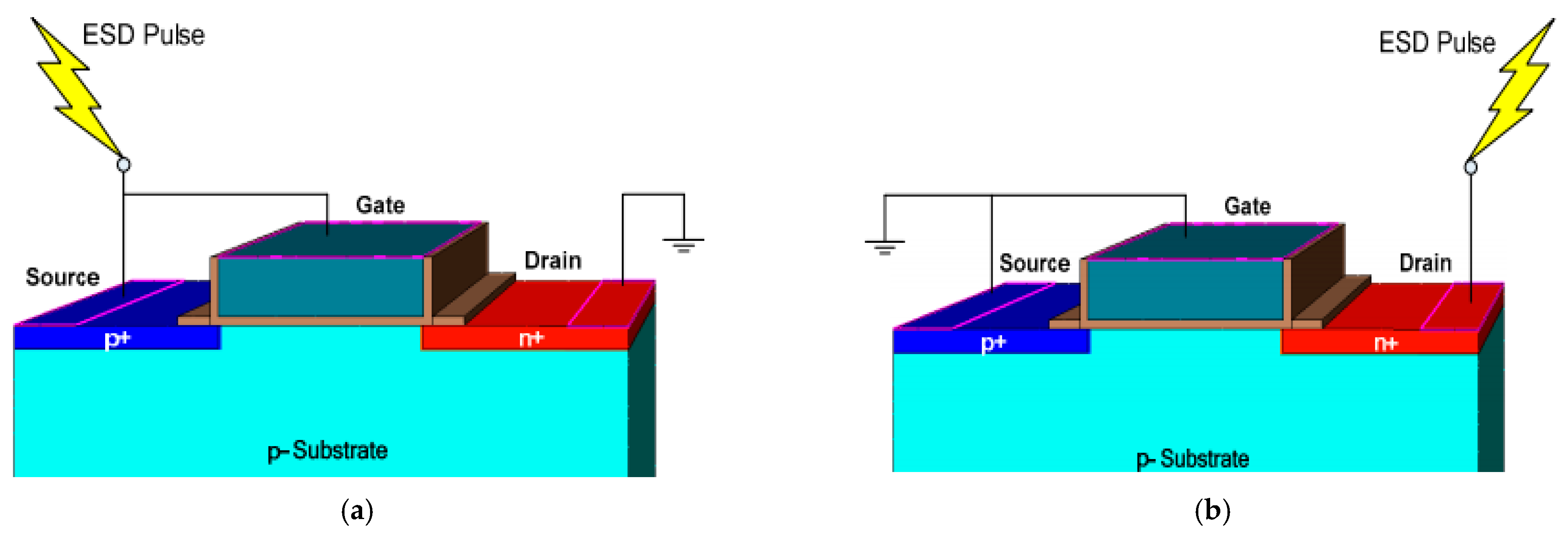
TFET is essentially a reverse biased gated p-i-n diode [22,23,24]. Under negative ESD stress, ESD current is injected into the source terminal of TFET with drain terminal grounded. TFET will operate in a positive diode conduction mode and has a high current discharge capability, as shown in Figure 1a [25,26]. Under the positive ESD stress, ESD current is injected into the drain terminal of TFET with the source terminal grounded. TFET will operate in avalanche breakdown mode to discharge the ESD current, as illustrated in Figure 1b. Since avalanche breakdown requires a relatively high electric field, the conduction voltage of TFET under positive ESD stress is high, making it unacceptable in advanced nanoscale technologies. Thus, the research on TFET under ESD stress mainly focuses on the positive discharge mode.
3. Device Structure and Simulation Setup
Figure 2a,b are schematic diagrams of SiGe S/D PNN TFET and Conventional TFET, both of which have SiGe Source/Drain. In order to facilitate heat dissipation, the device size is not set to a very small value [27,28]. The high K material of the gate medium is HfO2. The default device parameters are: gate oxide thickness = 4 nm, gate length LG = 100 nm, source, drain length = 100 nm, junction depth Xi = 10 nm, thickness= 1 μm, p+ source doping, p– channel doping and n+ doping of Conventional TFET are NS = 1 × 1020 cm−3, ND = 5 × 1019 cm−3, and NC = 1 × 1017 cm−3; p+ source doping of SiGe S/D PNN is NS = 1 × 1020 cm−3, and the n+ drain and n+ channel doping are defined as ND, both of which are 5 × 1019 cm−3. In order to avoid possible high defect density at the SiGe/Si interface, we set the default Ge mole fraction to 0.5.
Transmission line pulse(TLP) is a kind of non-destructive equivalent ESD impact test, which can accurately obtain the ESD characteristic parameters of the device. The drain terminal of the TFET was stressed with TLP pulses while keeping the gate and the source terminals grounded. The rise time and the pulse width were set as 10 ns and 100 ns. The voltage samples were obtained by averaging the transient data in the range of 60 ns to 90 ns [16].
All simulations of the above device structures are performed using Synopsys Sentaurus simulation software. In order to increase the accuracy of the simulation, the dynamic non-local path was used to analyze the band tunneling phenomenon of TFET devices under ESD impact. The probability of tunneling(TBTBT) depends on an electric field across the tunnel junction (E), carrier effective mass (m), the source band gap (Eg), as depicted in Equation (1).
The thermodynamic model was used to calculate the lattice temperature, and the Van overstraeten–de Man model was used to calculate the avalanche occurrence. In order to get more accurate simulation results, the bandgap narrowing model, the carrier mobility model, the high-field saturation model, and the doping associated carrier composite model were also used. The ESD characteristics of the device were evaluated by using the TLP simulation method. In the case of gate and source grounding, TLP current with 10 ns rise time and 100 ns pulse width was added to drain. The voltage samples are obtained by averaging the transient data in the range of 60 ns to 90 ns.
4. Simulation Results and Discussion
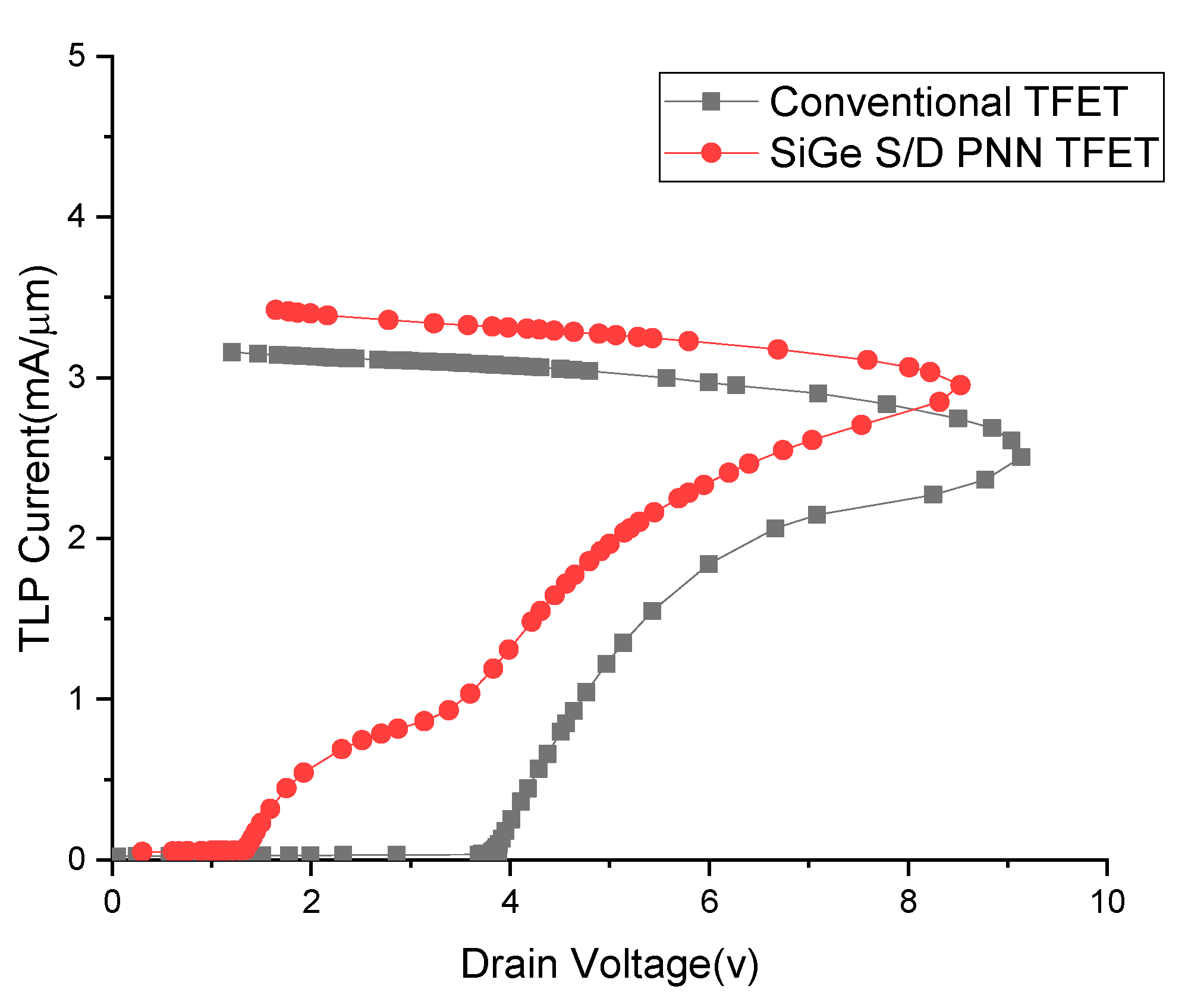
In order to verify the performance of PNN TFET, failure currents, trigger voltages, and electric fields of PNN TFET and Conventional TFET need to be simulated in this work. The source region tunneling junction of the Conventional TFET device was composed of a p+ SiGe doped source region and a low-doped p- Si substrate. Compared to PNN TFET, due to the wide tunnel junction and high trigger voltage, the failure current of Conventional TFET tends to be smaller. When the size of TFET device is reduced, the excessive trigger voltage may lead to the premature breakdown of the gate oxide layer, while the small failure current may lead to the premature damage of the device. In order to obtain better ESD design window, it is necessary to reduce the trigger voltage and increase the failure current. The TLP I-V curves of PNN TFET and Conventional TFET are shown in Figure 3. Under the same pulse current, the trigger voltage of PNN TFET was 1.3 V, and failure current was 3.0 mA/µm. Compared with Conventional TFET, the trigger voltage reduced by 66.3%, and the failure current increased by 20%. These key parameters will make it easier for TFET to adapt to modern ESD design Windows and improve the ESD performance of TFET devices.
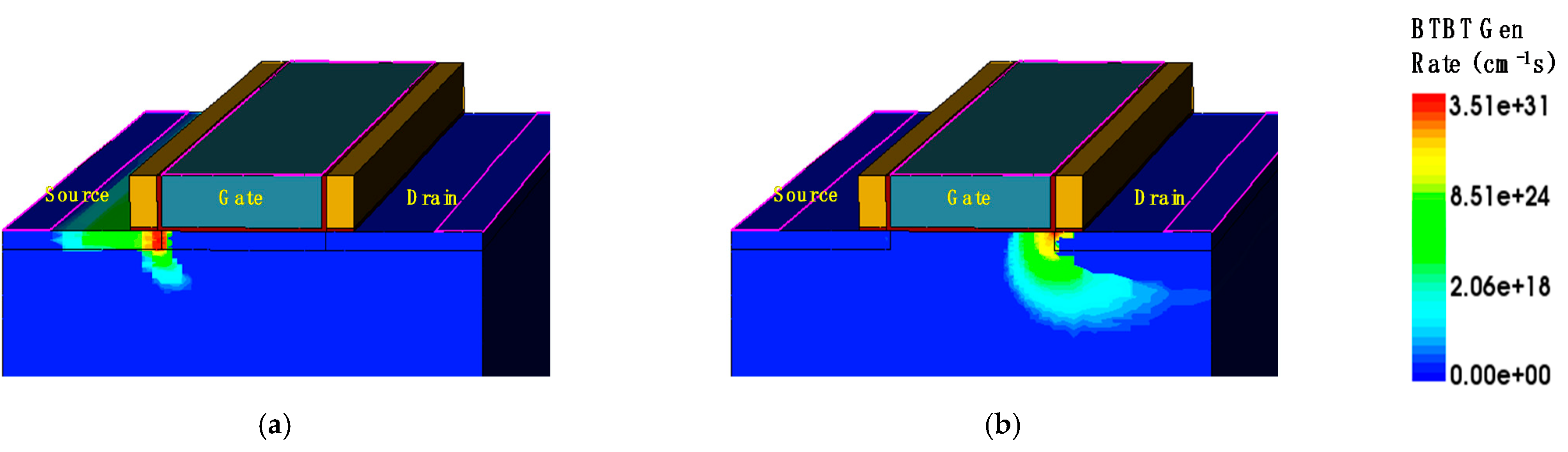
Figure 4 shows the distribution of the tunneling probability of PNN TFET and Conventional TFET under 1 mA current pulse. The difference is that PNN TFET tunneling mainly occurred at the source/channel junction, while Conventional TFET mainly occurred at the drain/channel junction. According to the simulation results, near the channel surface (within 2 nm), both PNN TFET and Conventional TFET had high band-to-band-tunneling (BTBT) Gen Rate (GBTBT)(>1 × 1030 cm−3s−1). However, from the middle of the channel (5 nm), the tunneling probability of the Conventional TFET decreased significantly while that of the PNN TFET remained at 1 × 1030 cm−3s−1. Therefore, the tunneling probability distribution of PNN TFET is more uniform, and the tunneling area is effectively improved.
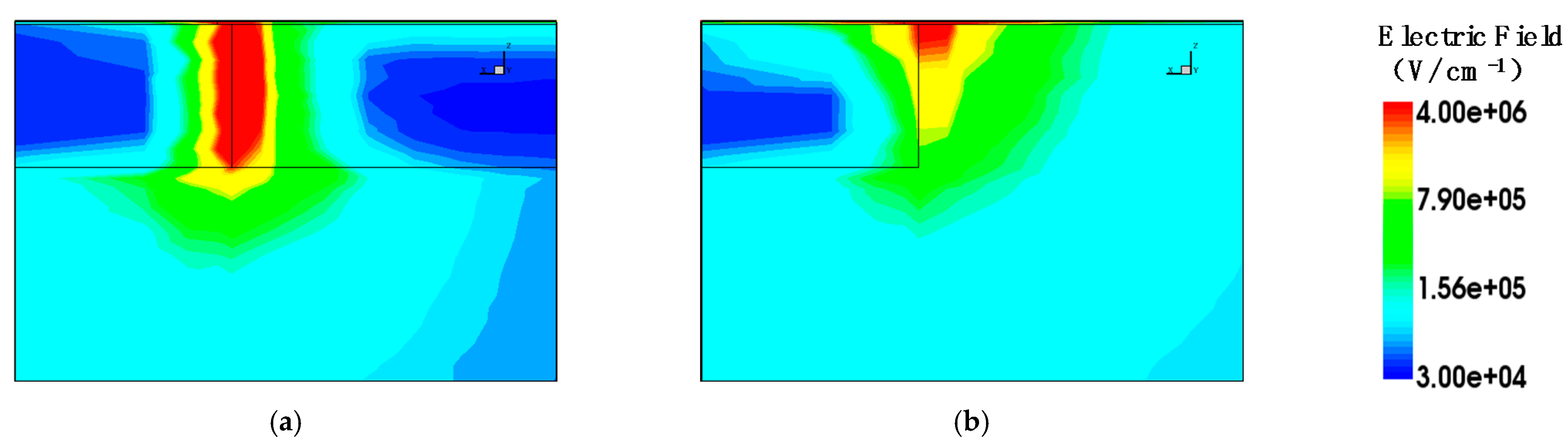
In order to study the improvement of the tunneling uniformity of the PNN TFET band, the electric field intensity distribution in the junction of drain and channel was extracted. When the band curvature was greater than the band gap of SiGe material; obvious band tunneling occurs. In other words, when the band bend exceeded the band gap of SiGe, the tunneling path obtained a large GBTBT. Because the band bending from drain to channel depends on the electric field. For SiGe PNN TFET, obvious tunneling occurred when the electric field at the tunneling junction was higher than 3.7 MV/cm−1. As shown in Figure 5, the strength of the PNN TFET’s entire electric field under 1 mA/µm TLP current was higher than 3.7 MV/cm−1, indicating that the tunneling area was greatly increased. For PNN TFET, the doping concentration in the N+ channel region was 5 × 1019 cm−3; for Conventional TFET, the channel was close to the eigenvalue, and the doping concentration was 1 × 1017 cm−3. When a TLP current pulse was applied, electrons accumulated in the channel. But the electron density in the middle and below of the channel was much lower than that on the channel surface. Since the channel region of PNN TFET was heavily doped, the electron density in and below the channel will be much higher than that of Conventional TFET when receiving the current pulse.
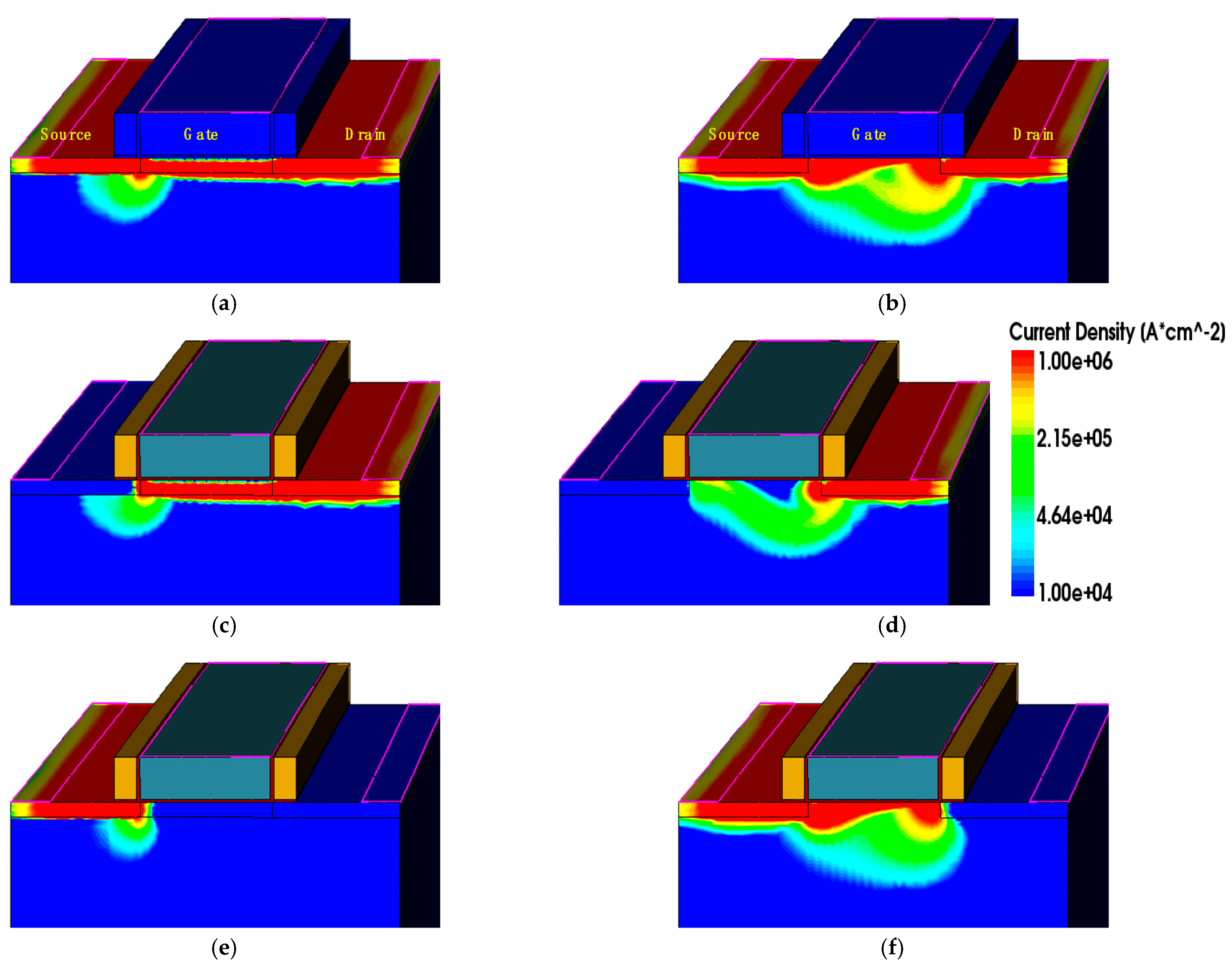
When the TLP current increased, the double-current path of Conventional TFET was more obvious. The device could be observed to have two distinct current paths. The upper path was the hole current path, and the lower path was the electron current path. Different from the Conventional TFET’s double-current path, the total current, electron current, and hole current of PNN TFET were all in one path; that is, there was only a single-current path, as shown in Figure 6. In the junction of channel/source, there existed a blocky current.
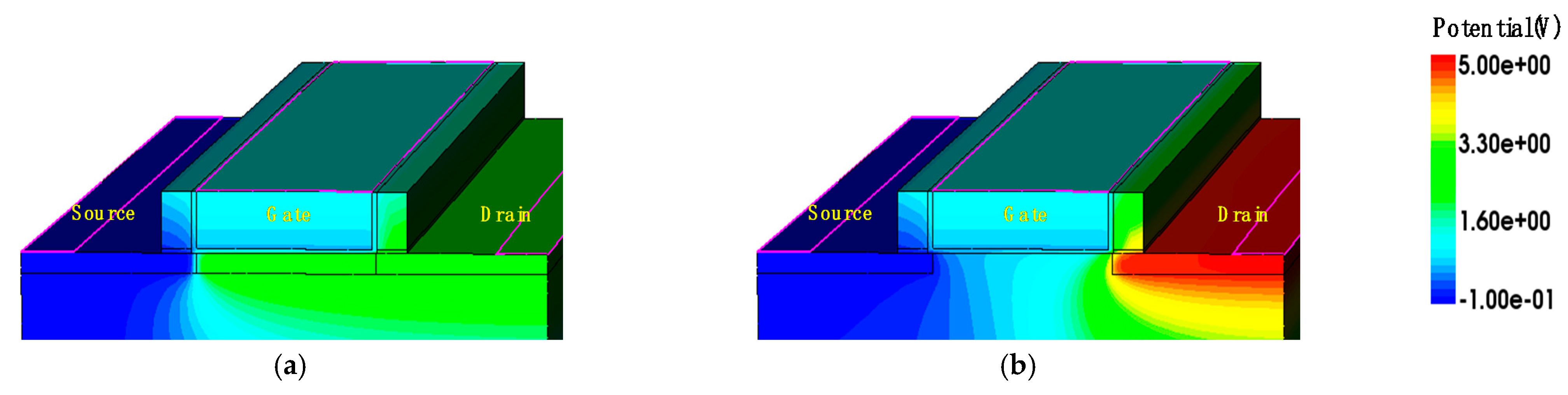
This phenomenon can be explained as follows: for the Conventional TFET with both gate and source grounded, the potential of drain level increases under the circumstance of ESD current injection. Figure 7 shows the electric potential contour of the SiGe S/D PNN TFET and Conventional TFET. The closely-spaced contour near the drain/channel interface indicates that the region has a high potential and is the first region where BTBT occurs, and BTBT generates a large number of hole electron pairs. The holes are swept to the oxide interface by a vertical electric field in Conventional TFET [18]. For PNN TFET, while the channel and the drain are n+ doping, the substrate is p– doping, it is equivalent to a reverse-biased PN(P-N+) junction, the electric field in the channel and the drain is basically the same. The difference of vertical electric field basically only exists at the junction of channel and source. This is the reason why the block current is generated here.
5. Optimization of SiGe S/D PNN TFET Device Parameters
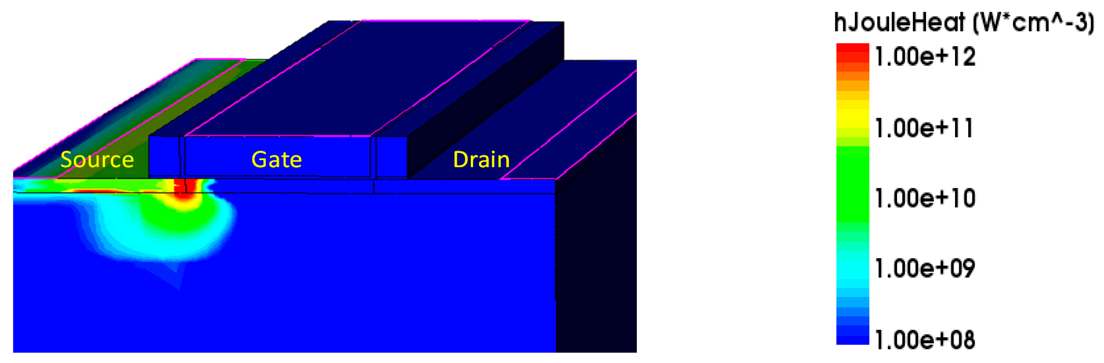
Under an ESD event, the Joule heat is the main heat component in the device, and it can be expressed as in reference [29].
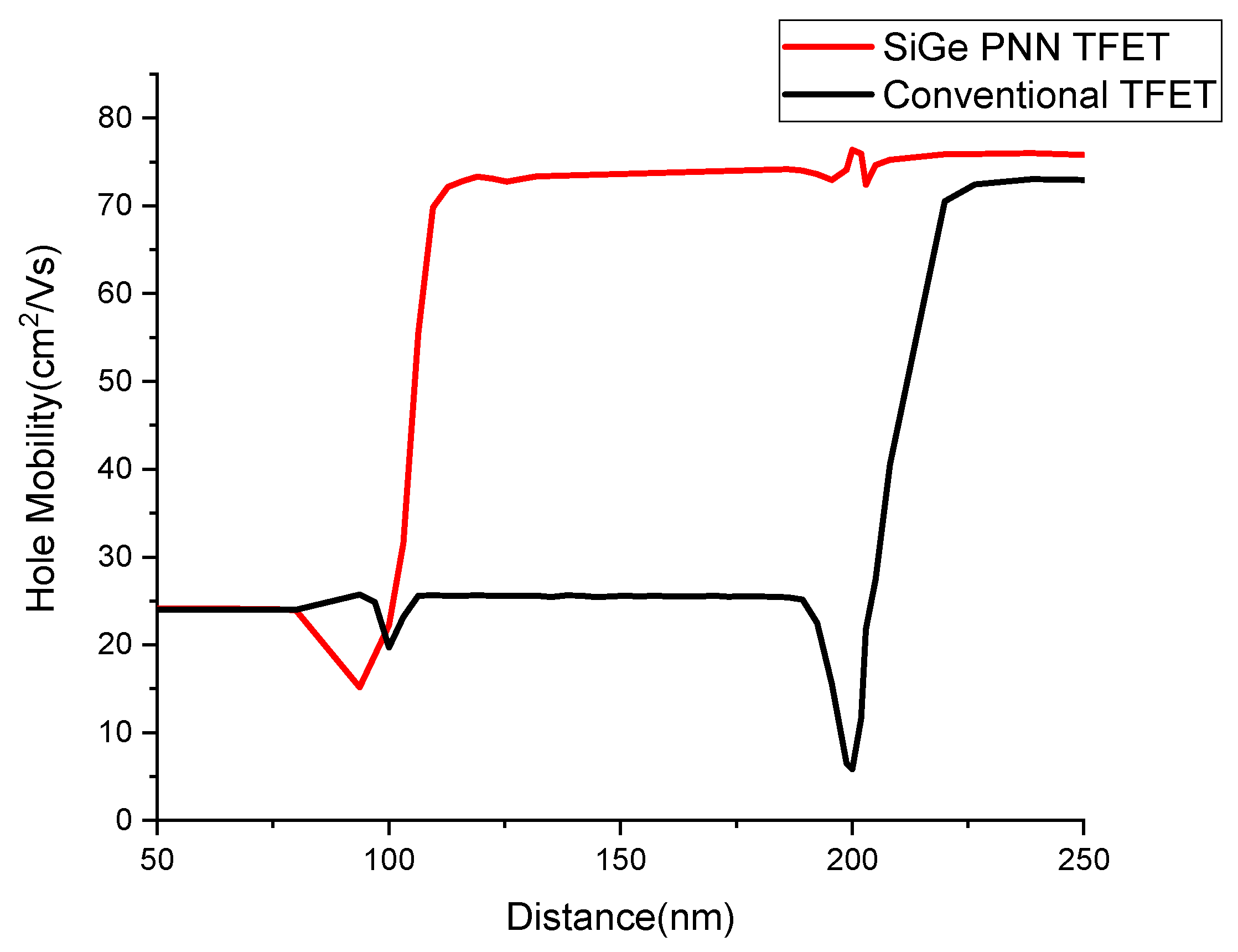
Where H is heat, J is current density, μ is mobility, and the subindices n and p are electrons and holes, respectively. The joule heat of the hole is higher than the joule heat of the electron because the hole generated by the impact moves from the drain interface to the source through the channel region, and the electron is collected by the drain and channel without any movement. These, in turn, cause a large amount of hole Joule heat generated at the interface regions, as shown in Figure 8. The hole mobility in SiGe S/D TFET is higher than that in Si TFET because the hole Joule heat is the dominant heat source and hole mobility in SiGe is higher than that in Si [30]. As shown in Figure 9, The hole mobility in the SiGe S/D PNN TFET is higher than that in the conventional TFET.
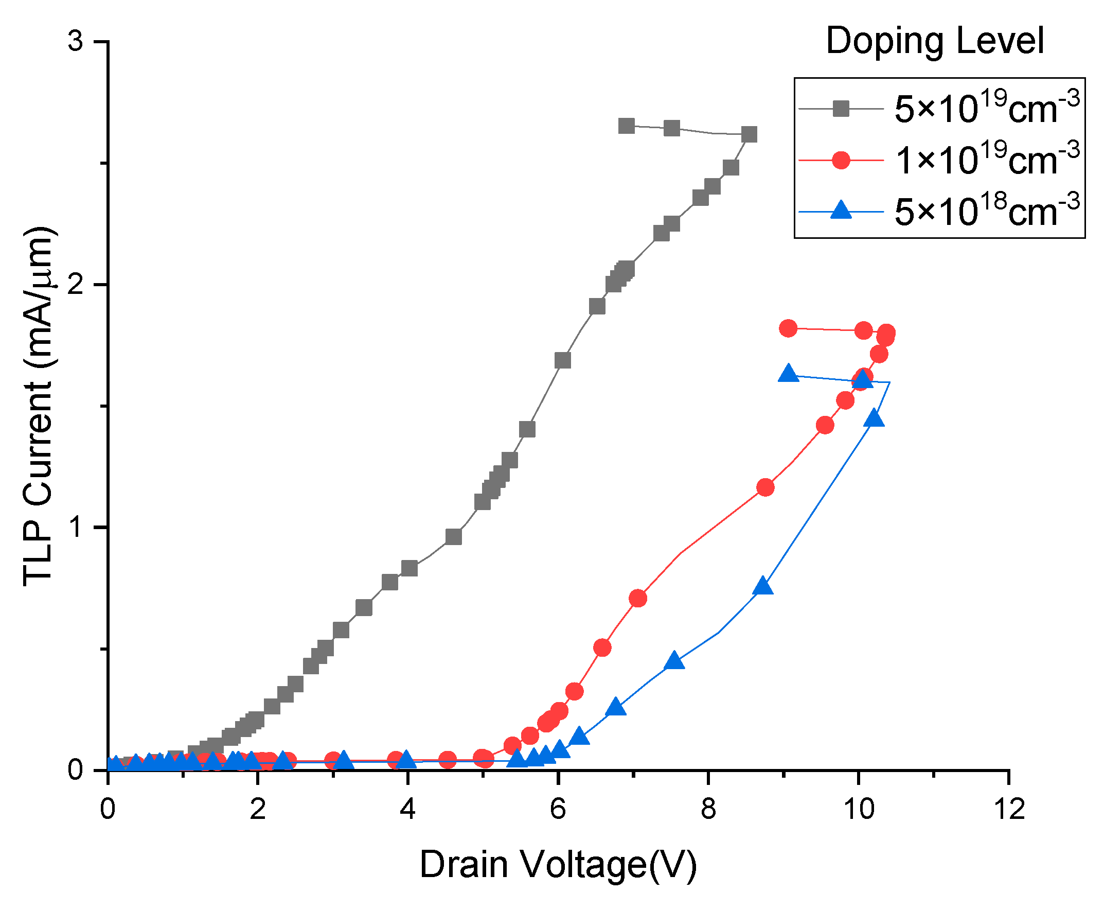
Figure 10 depicts the TLP I–V characteristics of PNN TFET for different drain doping while keeping gate length fixed (100 nm). It can be observed that a lower drain doping level increases the breakdown voltage. This can be attributed to the enhanced BTBT and the reduction in the critical electric field required for avalanche breakdown. With the increase of S/D doping concentration, the trigger voltage decreased, and the hole joule heat decreased, so the failure current increased.
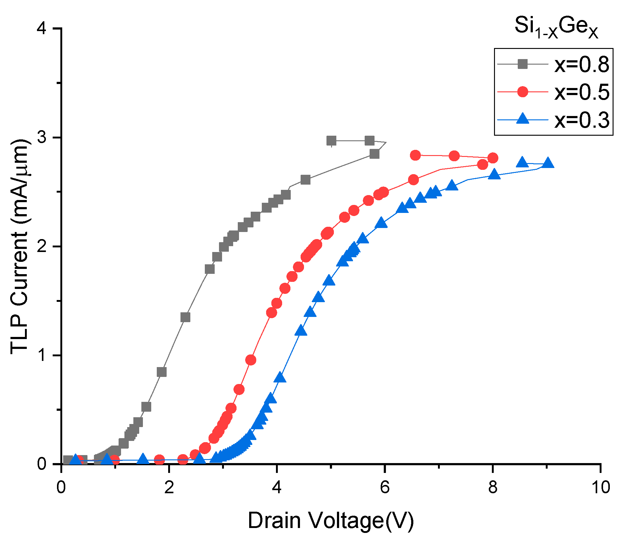
In SiGe PNN TFET, as shown in Figure 11, it can be seen that the increase of the mole fraction of Ge led to a decrease in the triggering voltage. It resulted in a slight reduction in the failure current. This trend can be easily understood from the preceding discussion. Because the hole Joule heat is the dominant heat source and hole mobility in SiGe is higher than that in Si, so the increase of the mole fraction of Ge will lead to the decrease of the triggering voltage.
6. Conclusions
In this paper, a new SiGe Source/Drain PNN field effect transistor was presented, and its ESD characteristics were studied by TCAD simulation. Compared with the Conventional TFET, the trigger voltage of the SiGe Source/Drain PNN TFET is reduced because the tunneling region has a high BTBT probability and a higher impact ionization coefficient. The failure current of the SiGe Source/Drain PNN TFET is also increased by the lower trigger voltage and a smaller Joule heat resulting from higher hole mobility in SiGe. The unique single current path phenomenon in PNN TFET has been discovered in this work. The results have demonstrated that the single current path is formed by the same electric field in the channel and the drain. SiGe S/D PNN TFET device parameters are optimized in this work; an increase of drain doping level and mole fraction of Ge can improve ESD performance. This enhanced ESD performance will be beneficial for constructing robust TFET-based ESD protection devices in the future.
Author Contributions
Conceptualization, methodology, validation, formal analysis and writing original draft preparation: Y.W.; writing review and editing: Y.W., Y.M., Q.J., M.Y., Z.Y. and H.L. resources and project administration: Q.J., M.Y., Z.Y. and H.L. All authors have read and agreed to the published version of the manuscript
Funding
This work was funded by the Fundamental Research Funds for the Central University of China (No. CCNU18JCXK02, No. CCNU18GF006, No. CCNU16A02016, and CCNU19TS073), in part by the Electrostatic Research Foundation of Liu Shanghe Academicians and Experts workstation, The Beijing Orient Institute of Measurement and Test (No. BOIMTLSHJD20181002).
Acknowledgments
You Wang would like to thank the partners from the Antlab for the fruitful discussions and Shanghe Liu from Beijing Orient Institute of Measurement and Test. You Wang also would like to thank the guidance from Yan Han at Zhejiang University, and helpful advice from Beijing Orient Institute of Measurement and Test.
Conflicts of Interest
The authors declare no conflict of interest.
References
- Cristoloveanu, S.; Wan, J.; Zaslavsky, A. A review of sharp switching devices for ultra-low power applications. IEEE J. Electron Devices Soc. 2016, 4, 215–226. [Google Scholar] [CrossRef]
- Hueting, R.J.E. The Balancing Act in Ferroelectric Transistors: How Hard Can It Be? Micromachines 2018, 9, 582. [Google Scholar] [CrossRef] [Green Version]
- Seabaugh, A.C.; Zhang, Q. Low-Voltage Tunnel Transistors for Beyond CMOS Logic. Proc. IEEE 2010, 98, 2095–2110. [Google Scholar] [CrossRef]
- Ionescu, A.M.; Riel, H. Tunnel field-effect transistors as energy-efficient electronic switches. Nat. Cell Biol. 2011, 479, 329–337. [Google Scholar] [CrossRef]
- Chen, S.; Wang, S.; Liu, H.; Li, W.; Wang, Q.; Wang, X. Symmetric U-Shaped Gate Tunnel Field-Effect Transisto. IEEE Trans. Electron Devices 2017, 64, 1343–1349. [Google Scholar] [CrossRef]
- Krishnamohan, T.; Kim, D.; Raghunathan, S.; Saraswat, K. Double-Gate Strained-Ge Heterostructure Tunneling FET (TFET) with record high drive currents and ≪60mV/dec subthreshold slope. In Proceedings of the 2008 IEEE International Electron Devices Meeting, IEEE, San Francisco, CA, USA, 15–17 December 2008; pp. 1–3. [Google Scholar]
- Dewey, G.; Chukung, B.; Boardman, J.; Fastenau, J.M.; Kavalieros, J.; Kotlyar, R.; Liu, W.K.; Lubyshev, D.I.; Metz, M.V.; Mukherjee, N.; et al. Fabrication, characterization, and physics of IIIV heterojunction tunneling Field Effect Transistors (H-TFET) for steep sub-threshold swing. In Proceedings of the 2011 International Electron Devices Meeting, IEEE, Washington, DC, USA, 5–7 December 2011; pp. 6–33. [Google Scholar]
- Tomioka, K.; Yoshimura, M.; Fukui, T. Steep-slope tunnel field-effect transistors using IIIV nanowire/Si heterojunction. In Proceedings of the 2012 Symposium on VLSI Technology (VLSIT), IEEE, Honolulu, HI, USA, 12–14 June 2012; pp. 47–48. [Google Scholar]
- Rajoriya, A.; Shrivastava, M.; Gossner, H.; Schulz, T.; Rao, V.R. Sub 0.5 V Operation of Performance Driven Mobile Systems Based on Area Scaled Tunnel FET Devices. IEEE Trans. Electron Devices 2013, 60, 2626–2633. [Google Scholar] [CrossRef]
- Asra, R.; Shrivastava, M.; Murali, K.V.R.M.; Pandey, R.K.; Gossner, H.; Rao, V.R. A Tunnel FET for VDD Scaling Below 0.6 V with a CMOS-Comparable Performance. IEEE Trans. Electron Devices 2011, 58, 1855–1863. [Google Scholar] [CrossRef]
- Yuan, W.; Song, J.; Lei, S.; Gang, Z.; Xing, Z. Design of grid-coupled electrostatic discharge protection structure. Acta Phys. 2007, 12, 7242–7247. [Google Scholar]
- Liou, J.J. Challenges of designing electrostatic discharge (ESD) protection in modern and emerging CMOS technologies. In Proceedings of the 2013 International Symposium on Next-Generation Electronics, Kaohsiung, Taiwan, 25–26 February 2013; pp. 1–3. [Google Scholar]
- Li, J.; Mishra, R.; Shrivastava, M.; Yang, Y.; Gauthier, R.; Russ, C. Technology scaling effects on the ESD performance of silicide-blocked PMOSFET devices in nanometer Conventional CMOS technologies. In Proceedings of the EOS/ESD Symposium Proceedings, Anaheim, CA, USA, 11–16 September 2011; pp. 1–5. [Google Scholar]
- Shrivastava, M.; Agrawal, M.; Mahajan, S.; Gossner, H.; Schulz, T.; Sharma, D.K.; Rao, V.R. Physical Insight Toward Heat Transport and an Improved Electrothermal Modeling Framework for FinFET Architectures. IEEE Trans. Electron Devices 2012, 59, 1353–1363. [Google Scholar] [CrossRef]
- Sithanandam, R.; Kumar, M.J. A new on-chip ESD strategy using TFETs-TCAD based device and network simulations. IEEE J. Electron Devices Soc. 2018, 6, 298–308. [Google Scholar] [CrossRef]
- Galy, P.; Athanasiou, S. Preliminary results on TFET—Gated diode in thin silicon film for IO design & ESD protection in 28nm UTBB FD-SOI CMOS technology. In Proceedings of the 2016 International Conference on IC Design and Technology (ICICDT), IEEE, Ho Chi Minh City, Vietnam, 27–29 June 2016; pp. 1–4. [Google Scholar]
- Kranthi, N.K.; Shrivastava, M. ESD Behavior of Tunnel FET Devices. IEEE Trans. Electron Devices 2016, 64, 28–36. [Google Scholar] [CrossRef]
- Yang, Z.; Zhang, Y.; Yang, Y.; Yu, N. Investigation of the Double Current Path Phenomenon in Gate-Grounded Tunnel FET. IEEE Electron Device Lett. 2017, 39, 103–106. [Google Scholar] [CrossRef]
- Mitra, S.K.; Bhowmick, B. Physics-based capacitance model of Gate-on-Source/Channel SOI TFET. Micro Nano Lett. 2018, 13, 1672–1676. [Google Scholar] [CrossRef]
- Darwin, S.; Samuel, T.S.A. A Holistic Approach on Junctionless Dual Material Double Gate (DMDG) MOSFET with High k Gate Stack for Low Power Digital Applications. Silicon 2020, 12, 393–403. [Google Scholar] [CrossRef]
- Lu, H.; Esseni, D.; Seabaugh, A. Universal analytic model for tunnel FET circuit simulation. Solid-State Electron. 2015, 108, 110–117. [Google Scholar] [CrossRef]
- Jung, Y.H.; Kang, I.M.; Cho, S. Analysis of tunneling field-effect transistor with germanium source junction using small-signal equivalent circuit. Microw. Opt. Technol. Lett. 2018, 60, 2922–2927. [Google Scholar]
- Suman Kr., M.; Brinda, B. Impact of Temperature and Fixed Oxide Charge Variation on Performance of Gate-on-Source/Channel SOI TFET and Its Circuit Application. J. Nanoelectron. Optoelectron. 2018, 13, 1630–1640. [Google Scholar]
- Patel, J.; Sharma, D.; Yadav, S.; Lemtur, L.; Suman, P. Performance improvement of nano wire TFET by hetero-dielectric and hetero-material: At device and circuit level. Microelectron. J. 2019, 85, 72–82. [Google Scholar] [CrossRef]
- Strangio, S.; Settino, F.; Palestri, P.; Lanuzza, M.; Crupi, F.; Esseni, D.; Selmi, L. Digital and analog TFET circuits: Design and benchmark. Solid State Electron. 2018, 146, 50–65. [Google Scholar] [CrossRef] [Green Version]
- Aslam, M.; Sharma, D.; Soni, D.; Yadav, S.; Raad, B.R.; Yadav, D.S.; Sharma, N.K. Effective design technique for improvement of electrostatics behaviour of dopingless TFET: Proposal, investigation and optimisation. Micro Nano Lett. 2018, 13, 1480–1485. [Google Scholar] [CrossRef]
- Yang, Z.; Yu, N.; Liou, J.J. Impact of the gate structure on ESD characteristic of tunnel field-effect transistors. In Proceedings of the 2018 7th International Symposium on Next Generation Electronics (ISNE), IEEE, Taipei, Taiwan, 7–9 May 2018; pp. 1–4. [Google Scholar]
- Yang, Z.; Yang, Y.; Yu, N.; Liou, J.J. Improving ESD Protection Robustness Using SiGe Source/Drain Regions in Tunnel FET. Micromachines 2018, 9, 657. [Google Scholar] [CrossRef] [Green Version]
- Synopsys. User Manual, version I-2013.03, Synopsys TCAD Sentaurus; Synopsys: San Jose, CA, USA, 2013. [Google Scholar]
- Galy, P. Electro Static Discharge (ESD) one real life event: Physical impact and protection challenges in advanced CMOS technologies. In Proceedings of the 2014 International Semiconductor Conference (CAS), IEEE, Sinaia, Romania, 13–15 October 2014; pp. 31–34. [Google Scholar]
Figure 1.
Schematics of tunnel field-effect transistor (TFET) under (a) negative and (b) positive electrostatic discharge (ESD) stresses.
Figure 1.
Schematics of tunnel field-effect transistor (TFET) under (a) negative and (b) positive electrostatic discharge (ESD) stresses.

Figure 2.
(a) device structure of PNN TFET and (b) Conventional TFET.

Figure 3.
TLP I–V diagram of PNN TFET and Conventional TFET.

Figure 4.
Band-to-band tunneling gen rate (GBTBT) distribution of (a) PNN TFET and (b) Conventional TFET at source/channel junction.
Figure 4.
Band-to-band tunneling gen rate (GBTBT) distribution of (a) PNN TFET and (b) Conventional TFET at source/channel junction.

Figure 5.
Distribution of electric field intensity at the source and channel of (a) PNN TFET and (b) Conventional TFET at 90 ns under 1 mA/µm TLP current.
Figure 5.
Distribution of electric field intensity at the source and channel of (a) PNN TFET and (b) Conventional TFET at 90 ns under 1 mA/µm TLP current.

Figure 6.
Contour plots of (a) total current density, (b) hole current density and (c) electron current density of PNN TFET and (d) total current density, (e) hole current density, and (f) electron current density of Conventional TFET at 90 ns under 1 mA/µm TLP current. For clarity, only part of the device is shown.

Figure 7.
Contour plot of potential of (a) SiGe PNN TFET and (b) Conventional TFET.

Figure 8.
Contour plot of hole Joule heat simulated at 90 ns under a TLP current density of 1 mA/µm.
Figure 8.
Contour plot of hole Joule heat simulated at 90 ns under a TLP current density of 1 mA/µm.

Figure 9.
Hole mobilities at a distance of 5 nm below the Si/HfO2 interface.

Figure 10.
TLP I-V curves of SiGe S/D PNN TFET with different doping levels.

Figure 11.
TLP I-V curves of SiGe S/D PNN TFET with different Ge mole fractions.

Publisher’s Note: MDPI stays neutral with regard to jurisdictional claims in published maps and institutional affiliations. |
© 2021 by the authors. Licensee MDPI, Basel, Switzerland. This article is an open access article distributed under the terms and conditions of the Creative Commons Attribution (CC BY) license (http://creativecommons.org/licenses/by/4.0/).
Share and Cite
MDPI and ACS Style
Wang, Y.; Mao, Y.; Ji, Q.; Yang, M.; Yang, Z.; Lin, H. Electrostatic Discharge Characteristics of SiGe Source/Drain PNN Tunnel FET. Electronics 2021, 10, 454. https://0-doi-org.brum.beds.ac.uk/10.3390/electronics10040454
AMA Style
Wang Y, Mao Y, Ji Q, Yang M, Yang Z, Lin H. Electrostatic Discharge Characteristics of SiGe Source/Drain PNN Tunnel FET. Electronics. 2021; 10(4):454. https://0-doi-org.brum.beds.ac.uk/10.3390/electronics10040454
Chicago/Turabian StyleWang, You, Yu Mao, Qizheng Ji, Ming Yang, Zhaonian Yang, and Hai Lin. 2021. "Electrostatic Discharge Characteristics of SiGe Source/Drain PNN Tunnel FET" Electronics 10, no. 4: 454. https://0-doi-org.brum.beds.ac.uk/10.3390/electronics10040454
Note that from the first issue of 2016, this journal uses article numbers instead of page numbers. See further details here.