Article

Efficient Design Strategy for Optimizing the Settling Time in Three-Stage Amplifiers Including Small- and Large-Signal Behavior

by
Gianluca Giustolisi
* and
Gaetano Palumbo
Dipartimento di Ingegneria Elettrica Elettronica e Informatica (DIEEI), Università degli Studi di Catania Viale A., I-95125 Catania, Italy
*
Author to whom correspondence should be addressed.
Submission received: 12 February 2021 / Revised: 23 February 2021 / Accepted: 3 March 2021 / Published: 6 March 2021
(This article belongs to the Section Microelectronics)

Abstract

:
An analytical criterion for the optimization of the small-signal settling time in three-stage amplifiers is carried out. The criterion is based on making equal the two exponential decays of the step response. Including slew-rate effects, a useful design strategy for the design of three-stage operational transconductance amplifier is provided. Extensive time-domain simulations on a transistor-level design in a 65-nm CMOS process confirm the validity of the proposed approach.

1. Introduction

Among the various analog and mixed-signal integrated circuits, the operational transconductance amplifier (OTA) is certainly one of the most fundamental building blocks. Over the past few decades, the approach to their design has changed according to the technological scaling that, in turn, has been driven by the manufacturing processes of integrated circuits (ICs). The lowering of the intrinsic gain in MOS transistors ( g m r d 10 ), the scaling down of the power supply voltage ( V DD < 1 V ) and the consequent preclusion to the adoption of cascade configurations, moved the interest of the research towards multistage amplifier topologies [1,2,3,4,5,6,7,8]. In this background, the ‘speed’ of OTAs has been evaluated and compared using the gain-bandwidth product ( GBW ) as the main performance metric.
In the last 15 years, the extending demand for circuits with fast response to step inputs (i.e., discrete-time or switched-capacitor circuits, data converters, voltage regulators, etc.) has pushed the scientific community towards the design and the optimization of the settling time in low-voltage and multistage CMOS OTAs [9,10,11,12,13,14,15,16,17,18,19]. A significant number of design procedures have been proposed. However, many of them use complex relationships to forecast the settling time from the amplifier parameters, thus becoming unpractical in a real design. Moreover, most of them do not include the slew-rate ( SR ) limitations that occur under large-signal condition and that, as known, can have a serious impact on the time response.
Since the 1970s, the SR in OTAs has been analyzed in detail [20,21,22,23,24,25,26,27]. However, this specific literature has either produced complex results that did not lead to manageable design equations or provided accurate SR models that were limited to specific topologies.
Recently, in [28], the authors developed an interesting and general approach for the design of three-stage OTAs from settling-time requirements including also SR effects. Although the technique provides accurate results, it relies on the graphical analysis of the contour plots of the so-called Normalized Settling Time ( NST ) that change with different settling errors. Consequently, no analytical design criterion exists and, if the amplifier is required to settle within a given settling error, a new contour plot must be produced.
In this paper, we provide an analytical design criterion for optimizing the small-signal settling time of a three-stage amplifier, based on making equal the two exponential decays of the step response. This allows the designer to deal with a well-defined strategy avoiding the generation of contour plots and the design through graphical methods. Moreover, the approach considers large-signal effects since it also includes the slew-rate modeling exploiting the results in [28]. The proposed strategy is used to design a three-stage OTA from settling-time specifications. Extensive time-domain simulations confirm the validity of the proposed design strategy.

2. Settling-Time Modeling in Three-Stage Amplifiers

In this section, we develop a model for the settling time in three-pole amplifiers. First, we model the small-signal settling time in an all-pole amplifier (i.e., the loop gain of the amplifier has no zeros). Then, we propose a new and analytical design criterion to optimize the settling time that is based on making equal the two exponential decays of the step response. Next, we extend this design criterion to practical cases of generic amplifiers with one or more zeros in the transfer function of the open-loop gain. Finally, we extend the settling-time model by including the effects of slew-rate limitations so that we take into account the large-signal behavior, also.

2.1. Modeling of a Pure Three-Pole Amplifier

Pure three-pole amplifiers have no zeros in the transfer function of the open-loop gain. They belong to the class of the all-pole amplifiers and are modeled by
T ( s ) = β a ( s ) = β a 0 1 + s ω d · 1 1 + a 1 s + a 2 s 2
where a ( s ) is the direct gain of the OTA, β is the feedback factor, a 0 = a ( 0 ) is the dc gain, ω d is the frequency of the dominant pole and where coefficients a 1 and a 2 represent the non-dominant poles, in general, complex-conjugate. As long as β a 0 1 , the significant range of frequencies lies for ω ω d and the dc gain with the dominant pole simplify into
β a 0 1 + s ω d 1 s / GBW
where GBW = β a 0 ω d stands for the gain-bandwidth product of the amplifier. Hence the open-loop gain is
T ( s ) = 1 s GBW 1 + a 1 s + a 2 s 2 .
As explained in [29], the non-dominant poles in (3) arise because of an internal feedback loop nested in the main (external) loop. This situation is represented in Figure 1a where the stage of the internal loop is made up of an inner amplifier characterized by an internal gain-bandwidth product, GBW i , and by an internal non-dominant pole, ω s .
Manipulating the internal feedback loop in Figure 1a we obtain the equivalent block schematic in Figure 1b, where the inner stage is expressed in terms of the internal gain-bandwidth product and of the internal separation factor, K i = ω s / GBW i . This latter parameter is accountable for the stability of the internal loop (i.e., in a two-pole amplifier, the separation factor impacts on the phase margin as K tan ( PM ) and, in this specific case, the internal separation factor affects the internal phase margin, only). As a rule of thumb, we can assume that the minimum separation factor required for stabilizing the inner stage is K i = 1 [30].
For K i > 1 the inner stage is stable and, at a coarse but functional approximation, we can disregard the term s 2 / ( ω s 2 K i ) in the ‘non-dominant poles’ block in Figure 1b. Consequently, the whole amplifier stability depends on the ratio between the overall second pole, GBW i , and the gain-bandwidth product, GBW , i.e., on the external separation factor, defined as K e = GBW i / GBW .
Using the two separation factors, the open-loop gain becomes
T ( s ) = 1 s GBW 1 + s K e GBW + s 2 K e 2 K i GBW 2
and, if T ( s ) has the form expressed in (3), we can evaluate
K e = 1 a 1 GBW ,
K i = a 1 2 a 2 .
Normalizing the complex frequency with respect to the GBW we obtain a dimensionless version of the transfer function that allows analysis of the time response of the amplifier in a very convenient manner. To do so, we define the dimensionless frequency as s ^ = s / GBW and the corresponding dimensionless time as t ^ = GBW · t so that the open-loop transfer function turns into
T ( s ^ ) = 1 s ^ 1 + s ^ K e + s ^ 2 K e 2 K i .
When the system (6) is closed in a feedback loop, its response to a unity step input is a function of the dimensionless time, t ^ , and of the separation factor vector, K = ( K e , K i ) , i.e., y = y ( t ^ , K ) . From the output response, y ( t ^ , K ) we can evaluate the dynamic settling error ( DSE )
DSE ( t ^ , K ) = y ( ) y ( t ^ , K ) y ( )
and the dimensionless settling time as
t ^ s ( ϵ , K ) = min t ^ 🟉 :   DSE ( t ^ , K ) ϵ t ^ t ^ 🟉
being ϵ , the accuracy level. Therefore, the final settling-time results
t s = t ^ s ( ϵ , K ) GBW .
From (9) it is apparent that minimizing the small-signal settling time means both maximizing the GBW and minimizing the quantity t ^ s ( ϵ , K ) by a proper optimization of the separation factor vector, K . Since the maximization of the GBW is a straightforward task, we must find a criterion for the optimization of the dimensionless settling time, t ^ s ( ϵ , K ) .
In the following, to compare different settling-times at different accuracy levels, ϵ , it is convenient to use the Normalized Settling Time ( NST ). This is defined as the settling time of the amplifier under test normalized with respect to the settling time of a single-pole amplifier with the same GBW . In a single-pole amplifier, the settling time is t s ( sp ) = | ln ϵ | / GBW , therefore the normalized settling-time results in
NST = GBW | ln ϵ | t s = t ^ s | ln ϵ |
where the latter equivalence was derived from (9).

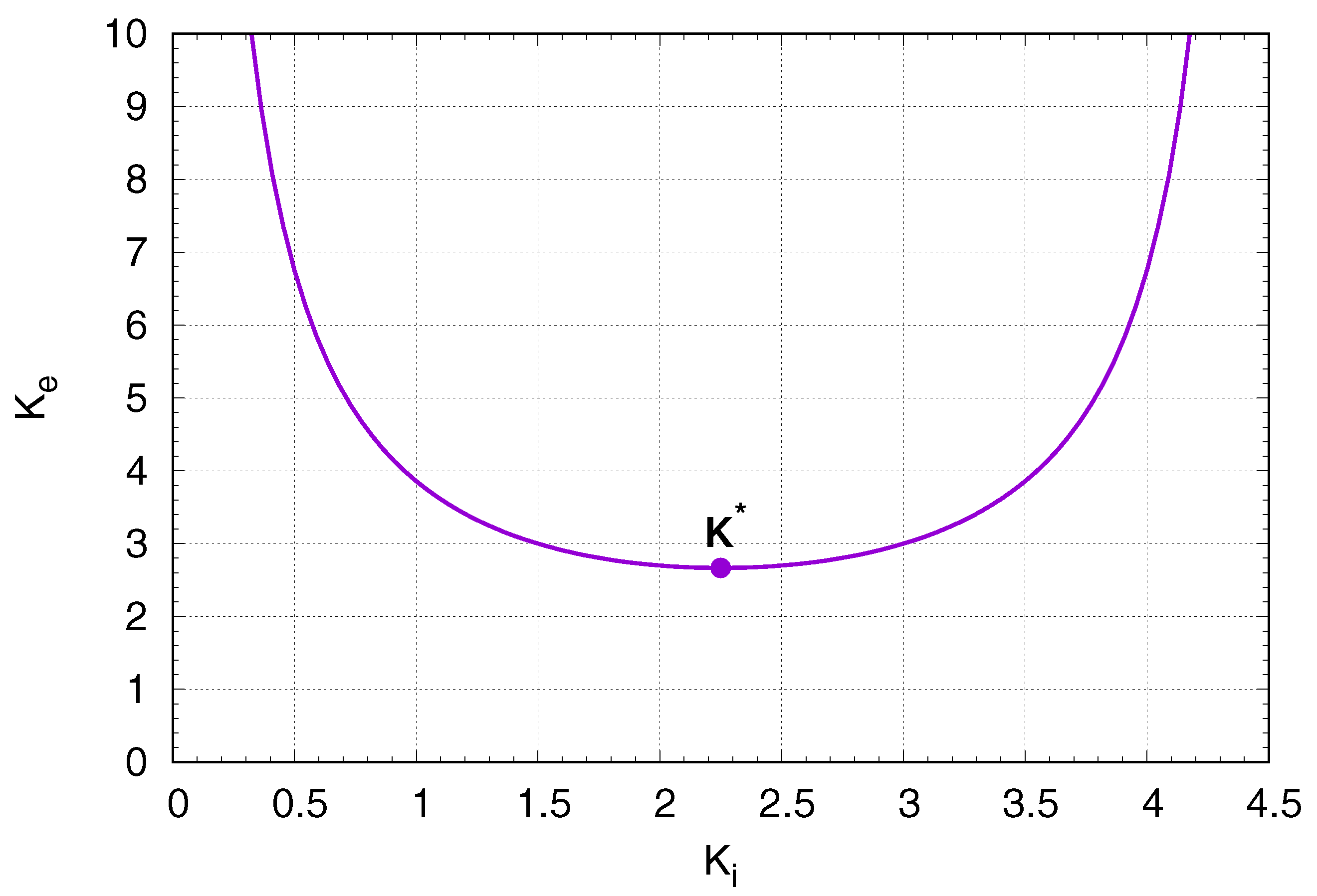
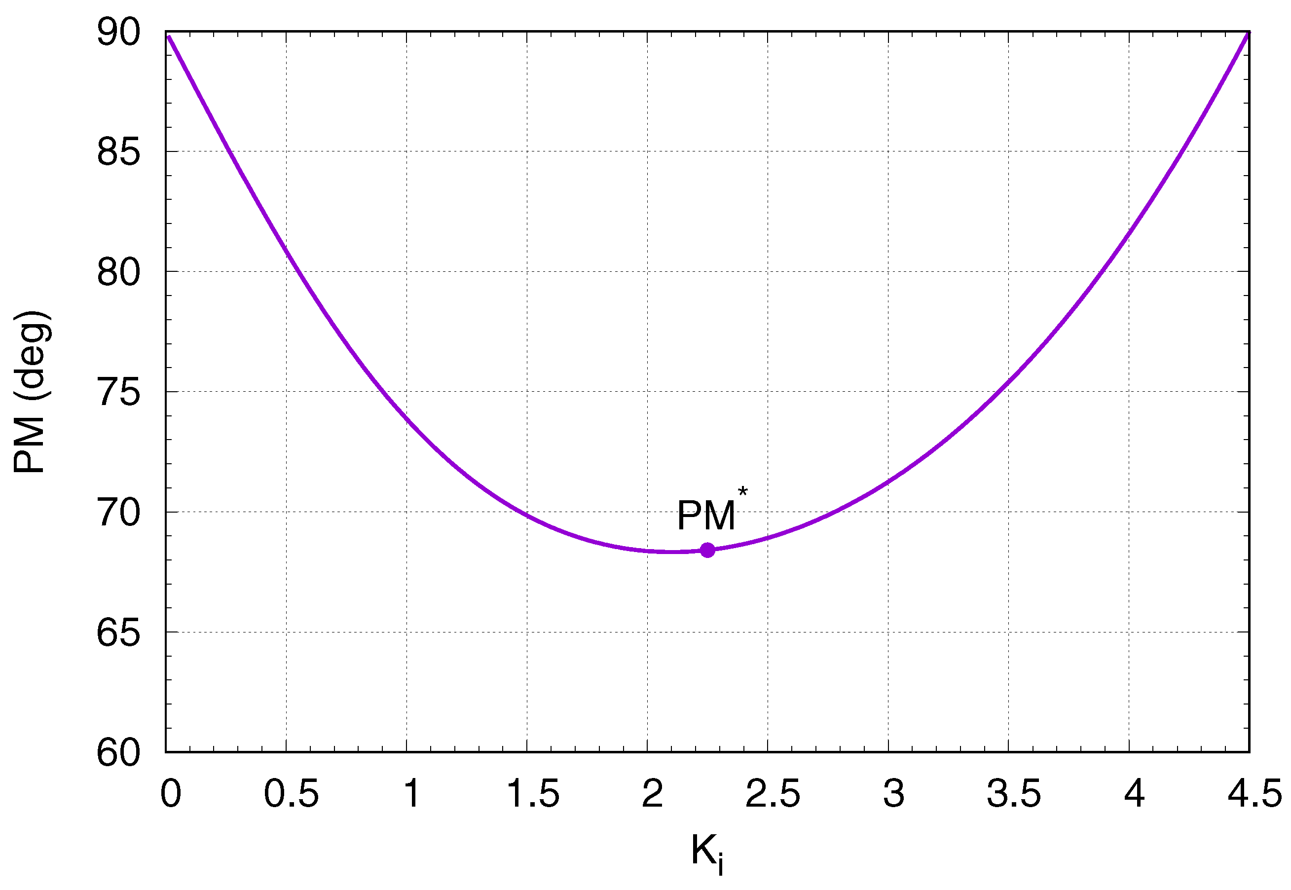
2.2. Optimization of the Dimensionless Settling Time

In a third-order system, the response to a unity step input in the time-domain takes the form
y ( t ) = 1 + A 1 e α 1 t + A 2 e α 2 t cos ω t + β α 2 ω sin ω t
whose corresponding Laplace transform is
Y ( s ) = 1 s + A 1 1 s + α 1 + A 2 s + β s + α 2 2 + ω 2 .
If the residues A 1 and A 2 are in the same order of magnitude, we may assume that the behavior of the amplifier’s time response is mainly ruled by the two exponential decays, α 1 and α 2 . Therefore, a design criterion for optimizing the amplifier speed is to set equal the two exponential decays so that α = α 1 = α 2 . In this way none of the exponential terms will be responsible for slowing down the time response. As known, the two exponential decays depend on the poles of the closed-loop transfer function, G ( s ) = s Y ( s ) , whose denominator is
D ( s ) = s + α ( s + α ) 2 + ω 2 = s 3 + 3 α s 2 + 3 α 2 + ω 2 s + α α 2 + ω 2 .
Using (4), the closed-loop gain is
G ( s ) = T ( s ) 1 + T ( s ) = K e 2 K i GBW 3 s 3 + K e K i GBW s 2 + K e 2 K i GBW 2 s + K e 2 K i GBW 3
and, equating the coefficients of the denominator of (14) to the coefficients of (13), we obtain the system of equations
K e K i GBW = 3 α ,
K e 2 K i GBW 2 = α 2 3 + ω α 2 ,
K e 2 K i GBW 3 = α 3 1 + ω α 2 .
Manipulating (15) we obtain the constraint that set equal the two exponential decays in terms of K e and K i
K e K i 3 2 9 K e K i 2 = 0
or, relating K e in terms of K i ,
K e = 3 K i 1 2 9 K i
whose plot is reported in Figure 2. Observe that since the condition in (16) is independent of the GBW , it represents a design criterion for the optimization of the dimensionless settling time, t ^ s .
Among the possible constraints set by (16), the most convenient is represented by the point K 🟉 in Figure 2, placed at the minimum value of K e . Using (17) to find this minimum yields
K 🟉 = K e 🟉 , K i 🟉 = 8 3 , 9 4 .
The plot of the phase margin, PM , versus K i for an ideal three-pole system designed with the constraint in (16) is shown in Figure 3. The point PM 🟉 = 68.4 deg identifies the phase margin observed at the optimum bias point set by ( K e 🟉 , K i 🟉 ) = 8 / 3 , 9 / 4 .
To further demonstrate the goodness of our design criterion, in Figure 4 we plot the normalized settling time, NST , versus the internal separation factor, K i , for a three-pole system designed with the constraint in (16) and for different accuracy levels, ϵ . The colored spots, all at the point of abscissa K i 🟉 = 9 / 4 , identify the normalized settling-times observed at the optimum bias point. Even if the proposed criterion does not identify the absolute minimum settling time, a satisfactorily settling time is established in a very simple manner. This is more evident considering that as reported in [29], a circuit designed for obtaining the minimum possible settling time always deviates from its target when unavoidable statistical variations of process or design parameters are taken into account.

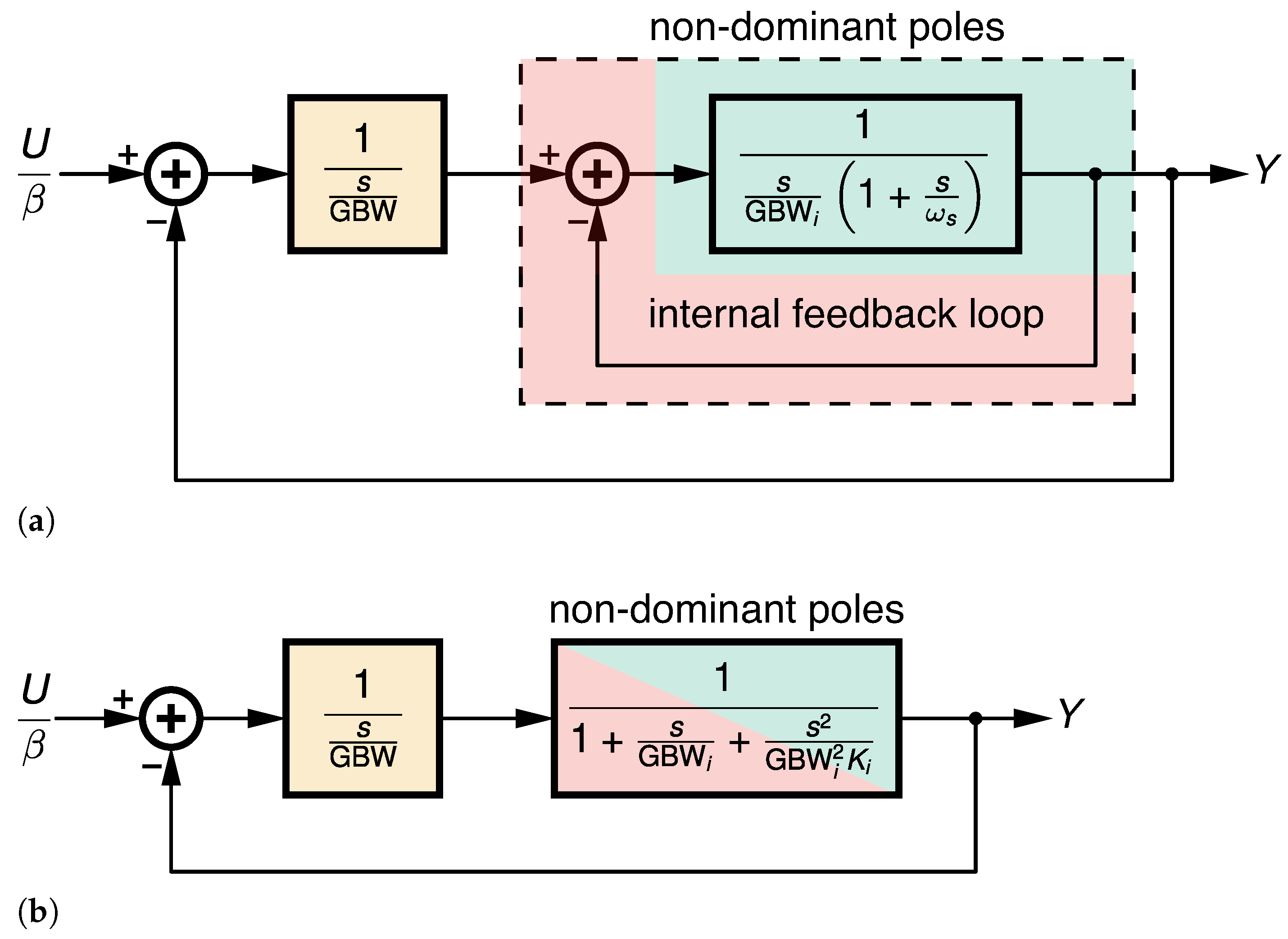
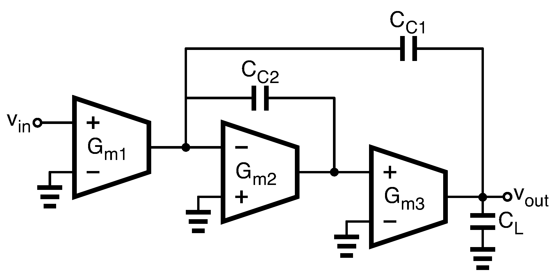
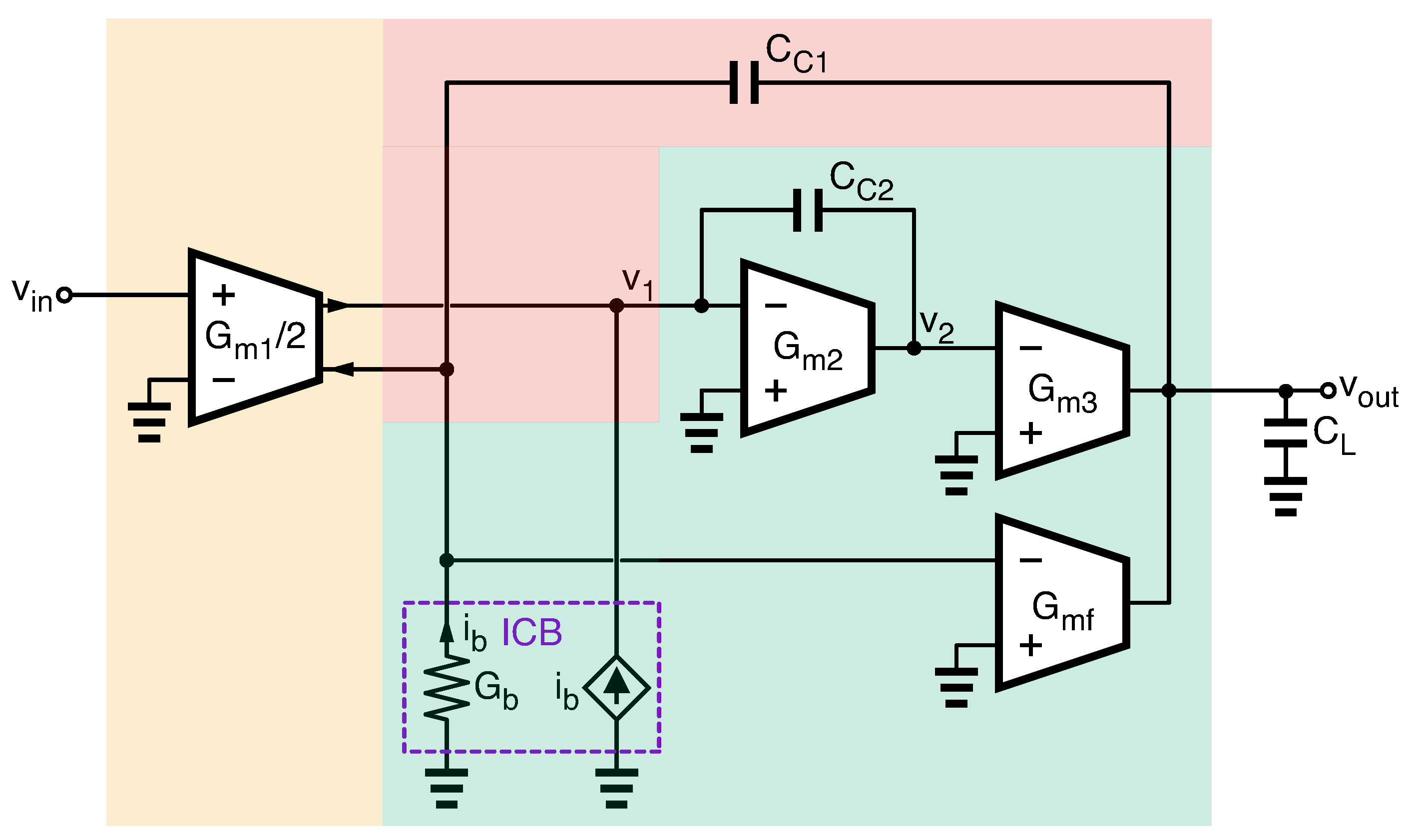
2.3. Extension to Generic Three-Pole Amplifiers

A generic three-pole amplifier has one or two zeros in the loop gain, i.e.,
T ( s ) = 1 + b 1 s + b 2 s 2 s GBW 1 + a 1 s + a 2 s 2 .
As demonstrated in [28] and briefly reported in Appendix A, if the frequency of the GBW lies below the zeros of T ( s ) , two global separation factors can be introduced
K ^ e = 1 + b 1 GBW 2 a 1 GBW + b 2 GBW 2 ,
K ^ i = a 1 GBW + b 2 GBW 2 2 a 2 GBW 2 1 + b 1 GBW .
The global separation factors can be used to make the condition of a time response with two equal exponential decays. More specifically, the dimensionless settling time of the generic three-pole amplifier is optimized by setting K ^ e and K ^ i to the same values that we would choose for the pure three-pole amplifier, i.e., setting K ^ e = K e 🟉 = 8 / 3 and K ^ i = K i 🟉 = 9 / 4 .
To verify the correctness of our approach, we designed the ideal amplifier in Figure 5 making K ^ e = 8 / 3 and K ^ i = 9 / 4 and compared its time response to that of an ideal pure three-pole amplifier with the same GBW and designed with K e = 8 / 3 and K i = 9 / 4 . We expect similar behaviors, i.e., very small NSTs, in the interval 0.4–0.6, for both circuits.
The amplifier in Figure 5 exploits the well-known Reversed Nested-Miller Compensation (RNMC) for which the coefficients of the transfer function in (19) are
GBW = G m 1 C C 1 ,
a 1 = C L C C 2 C C 1 G m 3 + C C 2 G m 3 C C 2 G m 2 ,
a 2 = C C 2 C L G m 2 G m 3 ,
b 1 = C C 2 G m 2 ,
b 2 = C C 1 C C 2 G m 2 G m 3 .
In our design, we assumed that the amplifier required a GBW of 100 Mrad / s (about 15.5 MHz ) for driving a load capacitor C L = 2 pF . Supposing that G m 1 = 100 μ A / V was set by noise specifications, from (21a) we obtained C C 1 = 1 pF . Then we substituted (21) into (20) and finalized our design by solving for K ^ e , K ^ i = 8 / 3 , 9 / 4 . The procedure led to C C 2 = 1.1 pF and G m 2 = G m 3 = 752 μ A / V . The time response of this ‘generic amplifier’ is depicted in Figure 6. For an effective comparison, the time response of a ‘pure three-pole amplifier’ with the same GBW is depicted also. It is observed a good matching between the two curves.
The details, in terms of settling time and NST , are reported in Table 1 for the two amplifiers. As expected, the approach for the optimization of the ‘generic amplifier’ produces a time response nearly as fast as the time response of the pure three-pole one.

2.4. Extension to Slew-Rate Modeling

Slew-rate effects in operational amplifiers can be included using the simple model introduced in [31] and analyzed in detail in [28].
The model assumes that the slew-rate limitation is in the first stage of the amplifier and, in particular, that it depends on the capacitor that determines the dominant pole. If this assumption is not satisfied, the amplifier can experience a positive feedback connection during its slewing period that degrades its speed performance and results in an inefficient design. In a good design, this inefficiency must be avoided either using slew-rate enhancers or class-ab topologies [30,32,33] in the stages placed after the first one.
As a second constraint, the model assumes that the amplifier is designed so to exhibit NST 1 in small-signal condition. In our case, this simply means that the amplifier can be designed in the optimum bias point set by ( K ^ e , K ^ i ) = 8 / 3 , 9 / 4 .
If the two assumptions described above are satisfied, the dimensionless settling time of the amplifier is bounded by
t ^ s | ln ϵ | for Δ Y ν < 1 | ln ϵ | + Δ Y ν 1 + ln Δ Y ν for Δ Y ν 1
where Δ Y is the output step voltage of the amplifier and
ν = I o 1 β G m 1
defines the equivalent saturation limit of the first stage, expressed in terms of its maximum short-circuit output current, I o 1 , of its small-signal transconductance, G m 1 , and of the overall feedback factor, β .
Also, in this case, to compare different settling-times at different accuracy levels, ϵ , we can define the NST by normalizing the settling time of the amplifier under test with respect to the small-signal settling time of a single-pole amplifier with the same GBW . From this definition and considering (10), the NST comes from dividing (22) by | ln ϵ | , i.e.,
NST 1 for Δ Y ν < 1 1 + Δ Y ν 1 + ln Δ Y ν | ln ϵ | for Δ Y ν 1 .

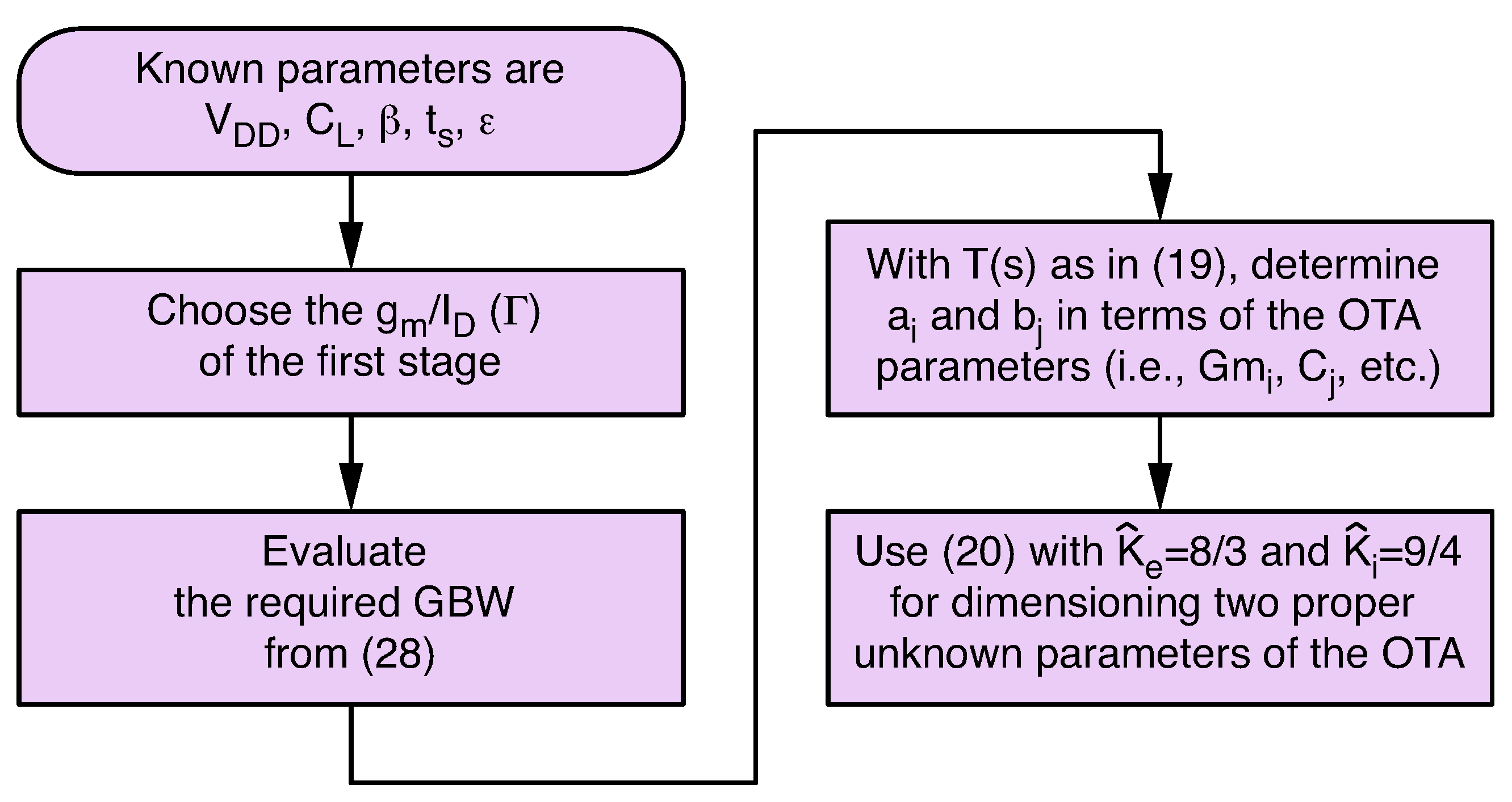
3. The Design Strategy with Settling-Time Constraints

In this section, we propose a design strategy based on settling-time constraints. It relies on two design equations. The first design equation is represented by the system in (20) and refers to the small-signal behavior. Using this system of equations, we guarantee that the small-signal settling time of the amplifier is less than (or comparable to) the settling time of a single-pole amplifier with the same GBW .
The second design equation stems from the dimensionless settling time in (22) and accounts for the large-signal effects in terms of slew-rate. Considering that t ^ s = GBW · t s , the settling-time constraint allows us to dimension the GBW from
GBW = | ln ϵ | + Δ Y ν 1 + ln Δ Y ν t s ,
where the maximum possible value for Δ Y / ν must be considered. Considering (23) we obtain that
Δ Y ν = β G m 1 I o 1 Δ Y .
The feedback factor, β , is a parameter that is specified by the application and cannot be freely chosen by the designer. In some particular cases the feedback factor can be programmed in a range of values (i.e., in switched-capacitor circuits, β can be selected by changing the connections of a proper array of capacitors) so that β = β max must be considered in the design equation.
Concerning the ratio G m 1 / I o 1 , it depends on the quiescent point of the first stage and, in the common case of a CMOS source coupled differential pair, it is
G m 1 I o 1 = Γ 2 ,
where Γ is the g m -over- I D ratio of the input transistors [34]. The plot of the g m -over- I D versus the gate-source overdrive is reported in Figure 7 for two complementary devices of a 65-nm CMOS process. Other nanometer CMOS processes have similar plots with no practical differences compared to the curves in Figure 7 [35]. Since, in the analog design context, transistors are biased so that V G S V TH , the choice of the g m -over- I D ratio has a limited range (typically, 8 V 1 Γ 16 V 1 ).
Finally, for the maximum output step, Δ Y , we can consider the highest possible value set by the power supply, V DD .
From all these considerations, based on the required settling time, the GBW is dimensioned according to
GBW = | ln ϵ | + β Γ 2 V DD 1 + ln β Γ 2 V DD t s .
The draft of the proposed design strategy is reported in the flow-chart in Figure 8. More specifically, once that the GBW is determined based on the settling time specification, the designer has two design equations that allows him to set two suitable parameters of the OTA. The remaining parameters can be chosen freely or based on other constraints set by noise, power dissipation or other critical figures of merit that, in general, depend on the application or on the amplifier topology.

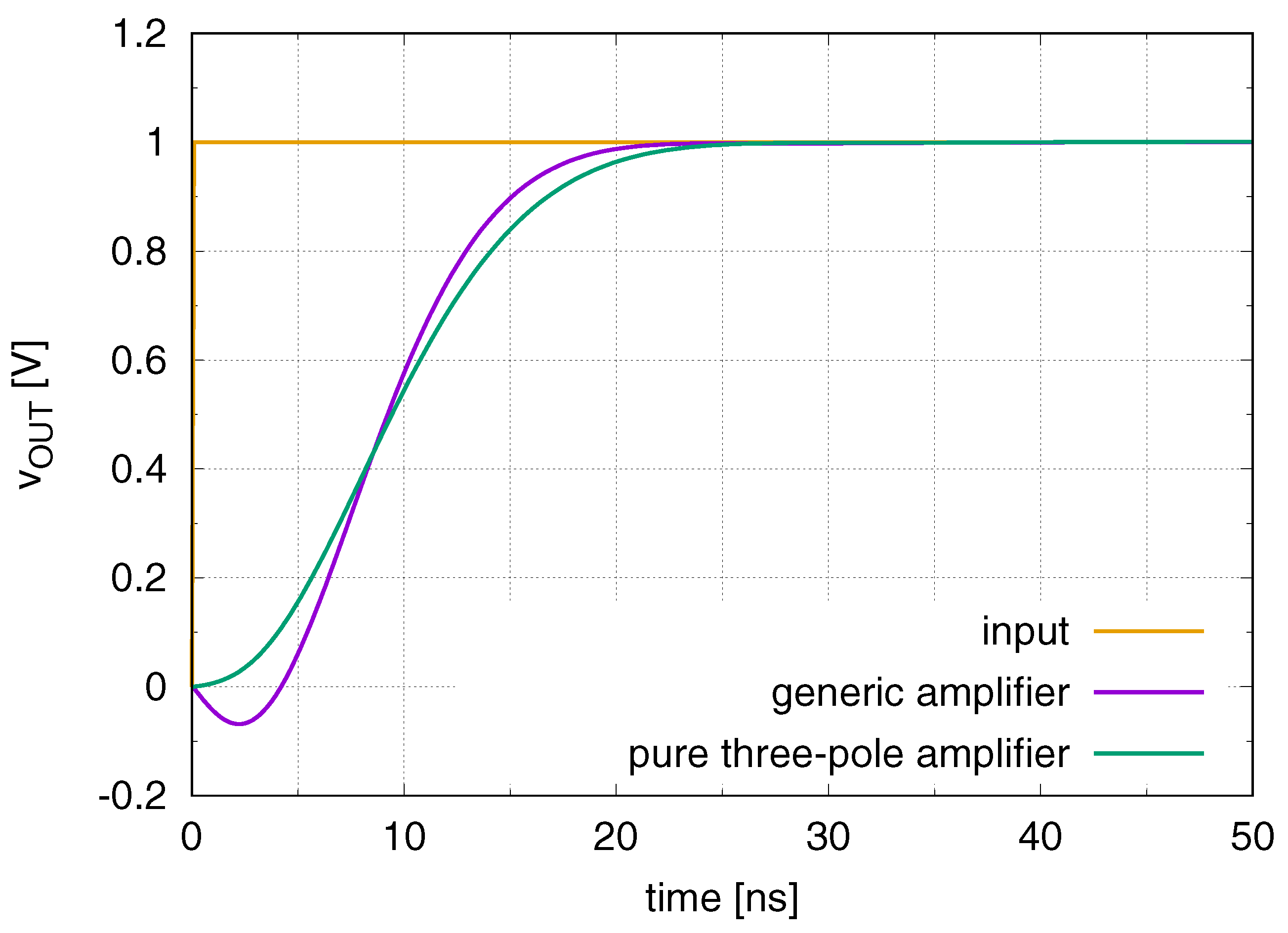
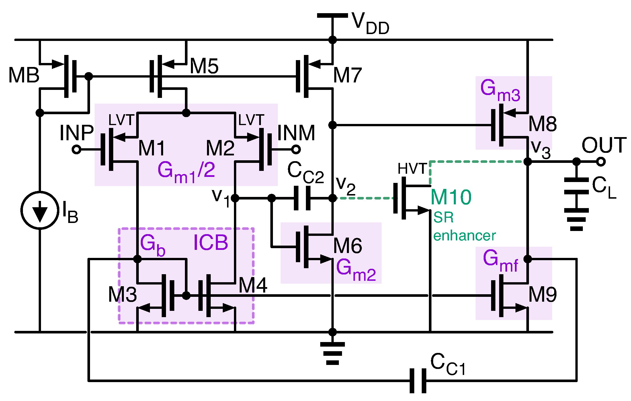
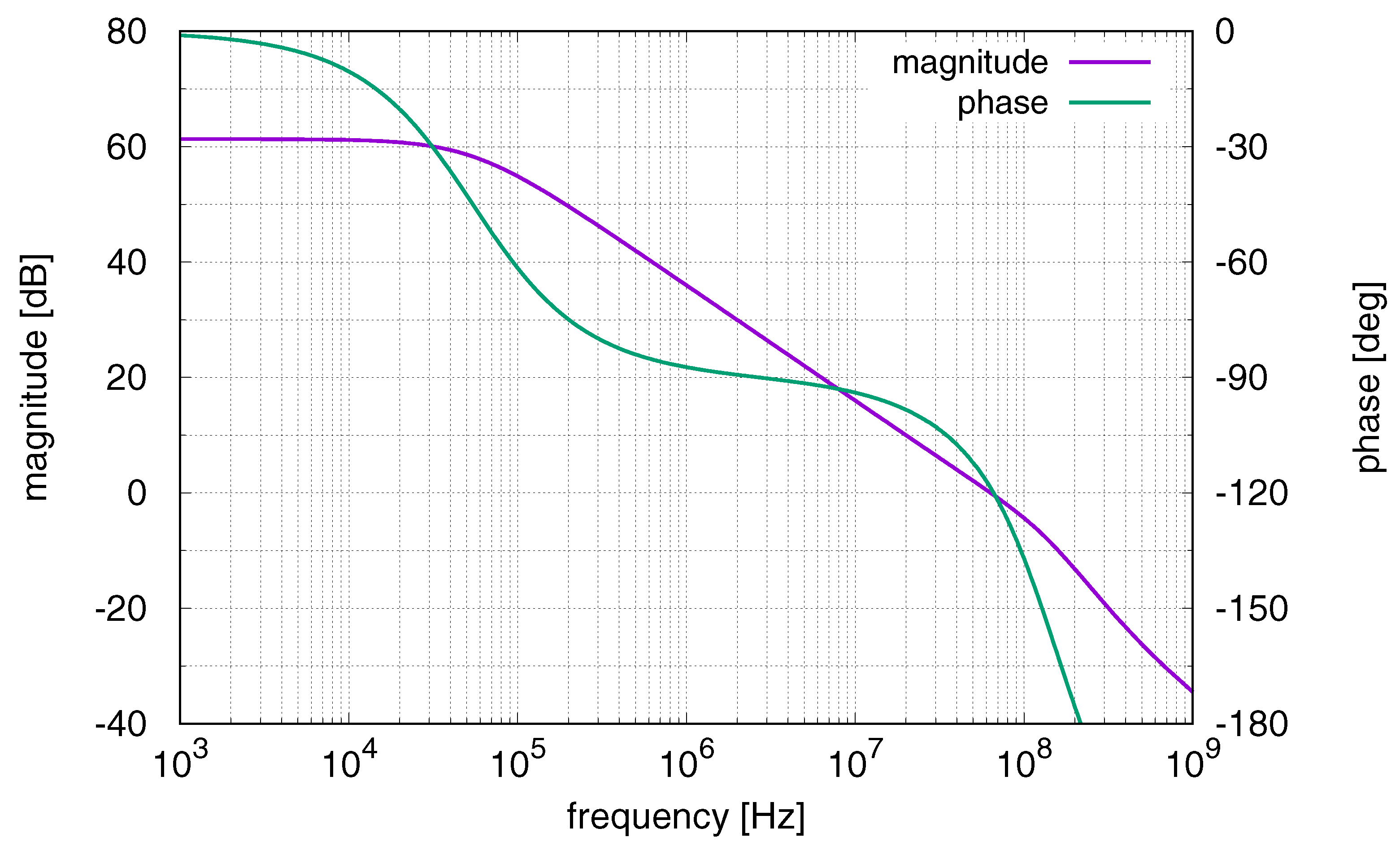
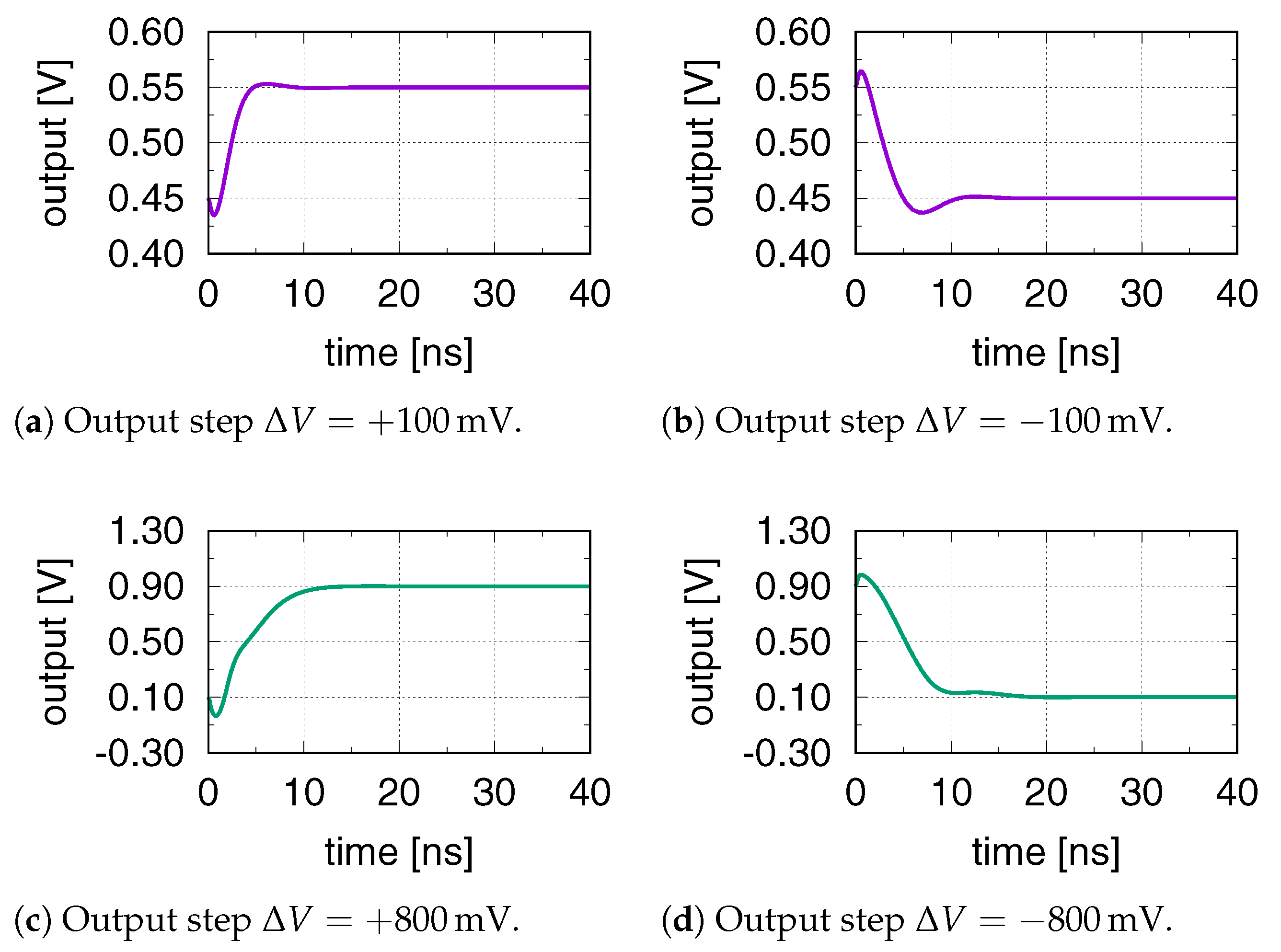
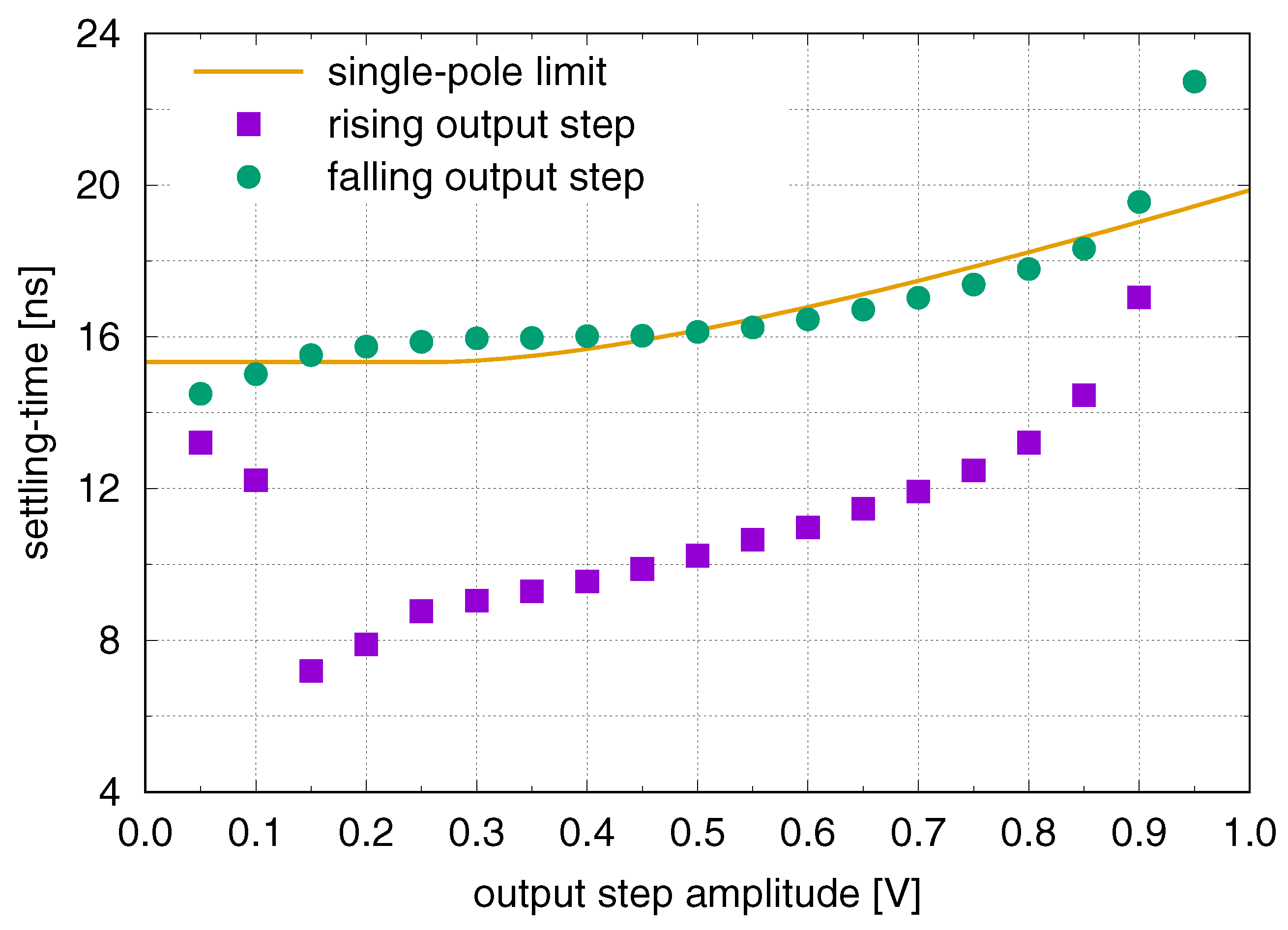
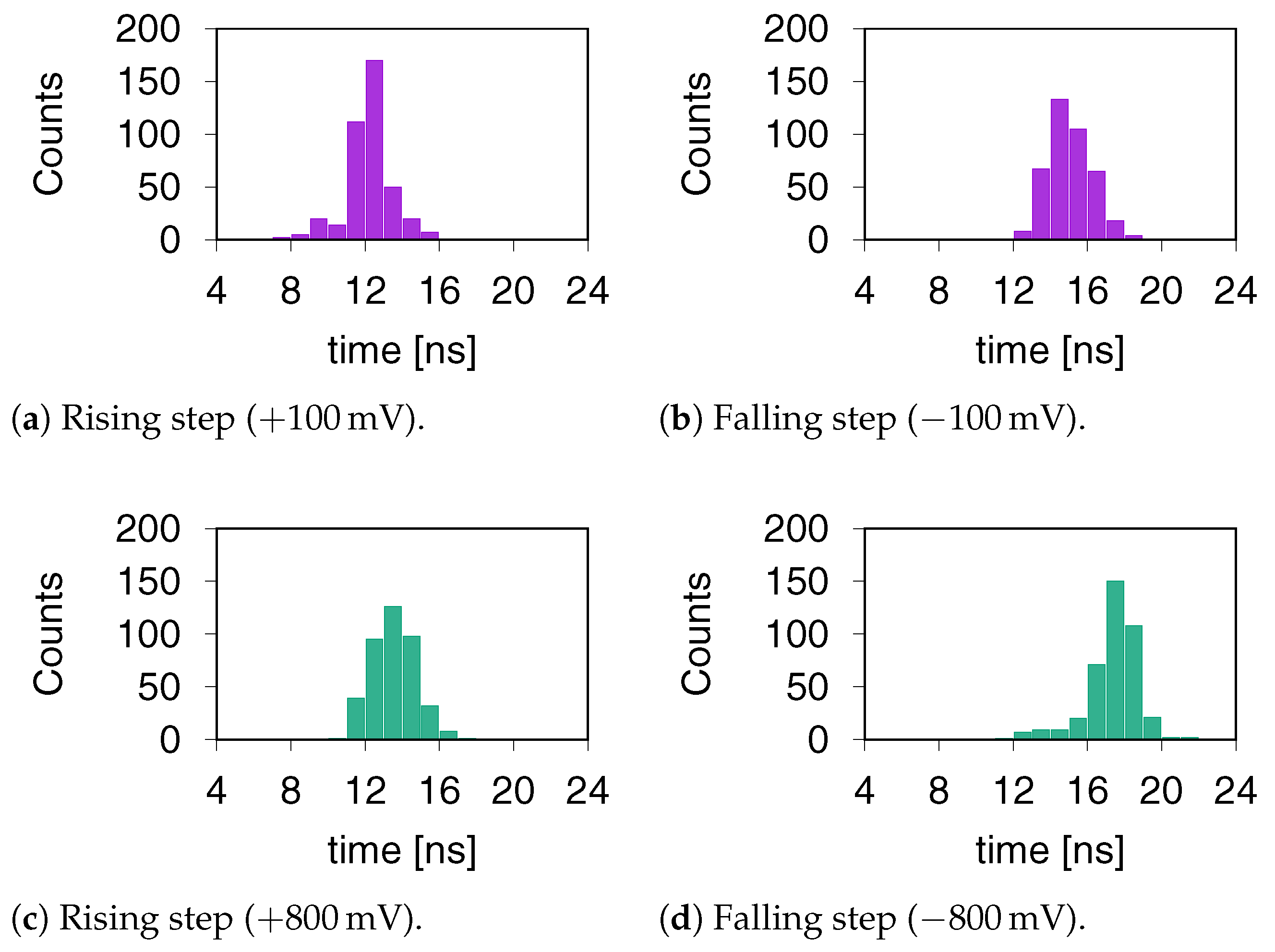
4. Design Example and Validation

To demonstrate and confirm the proposed design strategy, we apply it to the design of an appropriate three-stage OTA for the switched-capacitor (SC) application depicted in Figure 9.
Here the circuit acts as a forward-Euler SC integrator and, assuming T s is the sampling period, it works as follows. During the sampling phase, ϕ 1 at time t = ( n 1 / 2 ) T s , switches S 1 and S 2 close, the sampling capacitor, C s , charges at the input voltage, v IN , while the feedback capacitor, C f , maintains the charge processed at the previous time, t = ( n 1 ) T s . During the evaluation phase, ϕ 2 at time t = n T s , the sampling capacitor, C s , discharges through the virtual ground node and transfers its charge to capacitor C f , thus updating the output. The charge balance is represented by Δ Q C s = Δ Q C f and leads to
v OUT n = v OUT n 1 + C s C f v IN n 1 / 2 ,
where we omitted the obvious dependance on the sampling period, T s , and used the equivalence v OUT n 1 / 2 = v OUT n 1 .
During the sampling phase, ϕ 1 , the OTA does not change its output and remains in the ‘hold’ condition. During the evaluation phase, ϕ 2 , the output is fed back to the inverting terminal by the voltage divider composed by C f and C s so that the OTA experiences a feedback factor β = C f / ( C s + C f ) . At the same time, the OTA is loaded by an equivalent capacitor given by C L = C out + C s C f / ( C s + C f ) . These two parameters shall be considered during the design of the OTA.
In our design example, we assume that the capacitors of the integrator in the figure are C s = C f = C out = 0.4 pF . Therefore, the OTA has to be designed considering C L = 0.6 pF and β = 0.5 . We assume that the integrator operates with a sampling frequency of 25 MHz and that the target settling time is 20 ns within a 0.5% error. The power supply is V DD = 1 V .
We apply the design strategy to the transistor-level amplifier in Figure 10 made up of a differential pair (M1–M5) and two common-source stages (M6–M7 and M8–M9). The compensation is achieved through capacitors C C 1 and C C 2 , using a modified Reverse Nested-Miller Compensation, named RNMC-ICBFF. More specifically, capacitor C C 2 is connected between the output and the input nodes of the second stage. Capacitor C C 1 is connected between the output of the third stage and the input of the second one. In this latter connection the mandatory signal inversion is accomplished through the Inverting Current Buffer (ICB) made up of the current mirror M3–M4. Transistor M9, which provides the bias current to the third stage, acts also as a feed-forward (FF) stage, G mf .
The slew-rate enhancer, M10, is added in parallel to M9 to improve the SR performance at the output node during negative steps. Since M10 is a high-threshold transistor, it is normally off in bias condition. When node v 2 goes high and M8 switches off, M10 switches on and sinks the extra current required by the load.
Using the equivalent block schematic in Figure 11, we evaluate the open-loop transfer function of the amplifier. Neglecting the contributions of transconductors’ output resistances and parasitic capacitors, it takes the form in (19) where
GBW = β G m 1 C C 1 ,
a 1 = C C 2 G m 3 1 G m 3 G m 2 + C L C C 1 + G mf G b ,
a 2 = C C 2 C L G m 3 G b ,
b 1 = C C 1 2 G b + G mf 2 G b G m 3 G m 2 C C 2 G m 3 ,
b 2 = C C 1 C C 2 2 G b G m 3 1 + G m 3 G m 2 .
For the input transistors of the differential pair we choose Γ = 16 V 1 and, just for simplifying the design, the same value is adopted for the g m -over- I D of all the remaining transistors of the amplifier. Then, using (28), we obtain the minimum required GBW of 55 MHz . Observe that, in case of nanometer technologies, due to the low transistor intrinsic gain ( g m r d 10 ), Equation (30a) overestimates the actual GBW that, in this specific case, is better approximated by
GBW = β G m 1 C C 1 · 1 1 + C C 2 / C C 1 G m 3 R o 3 ,
being R o 3 the output resistance of the third stage. To make up for this error, which can be as high as 20%, we dimension the GBW by increasing the value obtained from (28) by 20%. Hence, we consider GBW = 66 MHz in our design equations.
The condition of making the same g m -over- I D ratio implies that transistors that share the same current have the same transconductance or, in other words, that G b = G m 1 and G m 3 = G mf . Therefore, defining
n = G m 3 G m 2 ,
m = G mf G b = G m 3 G m 1 ,
T = C C 2 G m 3 GBW ,
χ = C L C C 1 ,
we write the following normalized coefficients
a 1 GBW = 1 n + m + χ T β 2 ,
a 2 GBW 2 = β χ T β 2 ,
b 1 GBW = β 2 n m 2 T ,
b 2 GBW 2 = β 2 1 + n T ,
that can be substituted in (20) to obtain
K ^ e = 1 + b 1 GBW 2 a 1 GBW + b 2 GBW 2 = 1 + β 2 n m 2 T 2 1 n + m + χ β 2 1 + n T ,
K ^ i = a 1 GBW + b 2 GBW 2 2 a 2 GBW 2 1 + b 1 GBW = 1 n + m + χ β 2 1 + n 2 T β χ 1 + β 2 n m 2 T
where K ^ e = 8 / 3 and K ^ i = 9 / 4 .
Setting different values for n and m, we use Matlab to solve (37) for T and χ and to evaluate the remaining amplifier parameters from
C C 1 = C L χ ,
G m 1 = G b = C C 1 β GBW ,
G m 3 = G mf = m G m 1 ,
G m 2 = G m 3 n ,
C C 2 = T GBW G m 3 .
The results of the dimensioning procedure are reported in Table 2 for different values on n and m. The table reports also the estimated current dissipation of the OTA as I DD = 2 G m 1 + G m 2 + G m 3 / Γ , the Figure-of-Merit (FOM) that computes the speed-dissipation-load trade-off as FOM = GBW · C L / V DD · I DD and, neglecting the flicker noise for the sake of simplicity, the square root of the input noise spectral density, estimated as S n = 2 · 4 K T 2 / 3 1 / G m 1 1 + G m 1 / G b . As it can be observed, if the noise is satisfactorily to our application, the best choice in terms of current dissipation and FOM is the design corresponding to the row with n = 1 and m = 4 .
We design the circuit in the Cadence environment and the corresponding transistors’ aspect ratios are reported in Table 3.
The open-loop gain of the circuit in Figure 9 is simulated and reported in Figure 12 in terms of Bode diagram. The reported GBW is 62 MHz with a phase margin of 61 deg .
All the following transient simulations deal with the time response of the SC integrator during the evaluation phase, ϕ 2 . In particular, all the steps are referred to the output signal and are centered around the analog ground, V AGND = V DD / 2 = 0.5 V . This means that to simulate an output step of Δ V = + 100 mV , we first precharge the output node at v OUT ( n 1 ) = V AGND Δ V / 2 = 0.45 V and then we apply a constant input signal v IN = ( C f / C s ) Δ V . In this manner, from (29), the output jumps at v OUT ( n ) = v OUT ( n 1 ) + Δ V = 0.55 V .
The output step responses of the closed-loop amplifier to different step amplitudes are shown in Figure 13. Figure 13a,b depict the transient behavior of a ± 100 - mV output step for the rising edge and the falling one, respectively. The simulated settling-times are 12.2 ns ( NST = 0.92 ) and 15.0 ns ( NST = 1.13 ), respectively, for an accuracy level of 0.5%. Figure 13c,d show the transient behavior of a ±800-mV output step. In this case, the signal excursion is close to the rail-to-rail situation but still ensuring that no transistor exit from the saturation region. As expected, the slew-rate increases the 0.5 % settling time up to 13.2 ns ( NST = 0.99 ) and 17.8 ns ( NST = 1.34 ), for the rising edge and the falling one, respectively.
Figure 14 shows the plot of the 0.5 % settling time versus the step amplitude at the output node. The curve of the single-pole case, evaluated from (22), is also reported. As expected, for the rising edge, the settling time remains well below the single-pole limit up to 0.9 V. Above this value, some transistors enter the triode region, and the settling time goes out specifications. The falling output step suffers from slew-rate limitation at the output node. This is mitigated by the SR enhancer that allows the settling time to follow the single-pole limit up to 0.9 V, also in this case.
A 400-run Monte-Carlo simulation is performed to estimate how the circuit behaves under both global and local process variations. The results are condensed in the histograms in Figure 15. Figure 15a,b refer to the ± 100 - mV output step cases. Figure 15c,d refer to the ± 800 - mV output step cases. Except for a small number of samples in the 800-mV falling step case (Figure 15d), all the runs fall inside the settling-time specifications of 20 ns , a very good result considering that the circuit was not designed to be robust against process variations. However, it is easy to extend the design strategy to the worst-case corner of a PVT scenario or to integrate it with the approach described in [29].

5. Conclusions

In this paper, we provided an analytical design criterion for the optimization of the small-signal settling time in a three-stage amplifier, based on making equal the two exponential decays of the step response. Included the slew-rate effects to the design criterion we carried out a design strategy that was used to design a three-stage OTA from settling-time specifications. Extensive time-domain simulations confirmed the validity of the proposed design strategy.

Author Contributions

All authors contributed equally to this work. All authors have read and agreed to the published version of the manuscript.

Funding

This work was supported in part by Università degli Studi di Catania through the Project “Programma Ricerca di Ateneo UNICT 2020-22 linea 2”.

Data Availability Statement

The data presented in this study are available on request from the corresponding author. The data are not publicly available due to the non-disclosure agreement signed with owner of the technology process.

Conflicts of Interest

The authors declare no conflict of interest. The funders had no role in the design of the study; in the collection, analyses, or interpretation of data; in the writing of the manuscript, or in the decision to publish the results.

Appendix A. Global Separation Factors

Closing in feedback the pure three-pole system in (4) leads to the following closed-loop transfer function
G ( s ) = G 0 1 + c 1 s + c 2 s 2 + c 3 s 3 ,
where
c 1 = 1 GBW ,
c 2 = 1 K e GBW 2 ,
c 3 = 1 K e 2 K i GBW 3 .
In this situation, the two separation factors can be evaluated from the coefficients of the closed-loop transfer function as
K e = c 1 2 c 2 ,
K i = c 2 2 c 1 c 3 .
In the case of a generic three-pole amplifier, the transfer function includes two zeros in the loop gain, as in (19), and the resulting closed-loop transfer function is
G ( s ) = G 0 1 + b 1 s + b 2 s 2 1 + c 1 s + c 2 s 2 + c 3 s 3
where
c 1 = 1 GBW + b 1 ,
c 2 = a 1 GBW + b 2 ,
c 3 = a 2 GBW .
As long as the GBW remains below the zeros of G ( s ) we can assume that the amplifier time response is mainly determined by the poles of its closed-loop transfer function. This consideration allows us to define the equivalent or global separation factors using the coefficients of its closed-loop gain, as we did in (A3), so that
K ^ e = c 1 2 c 2 = 1 + b 1 GBW 2 a 1 GBW + b 2 GBW 2 ,
K ^ i = c 2 2 c 1 c 3 = a 1 GBW + b 2 GBW 2 2 a 2 GBW 2 1 + b 1 GBW .
Therefore, we can optimize the step response of the generic three-pole amplifier by design the amplifier so that K ^ e = 8 / 3 and K ^ i = 9 / 4 . Once again, since the coefficients are normalized with respect to the GBW , the optimization will affect the dimensionless settling time, only.

References

  1. Arnaud, A.; Fiorelli, R.; Galup-Montoro, C. Nanowatt, Sub-nS OTAs, With Sub-10-mV Input Offset, Using Series-Parallel Current Mirrors. IEEE J. Solid-State Circuits 2006, 41, 2009–2018. [Google Scholar] [CrossRef]
  2. Giustolisi, G.; Palumbo, G. Dynamic-biased capacitor-free NMOS LDO. IET Electron. Lett. 2009, 45, 1140–1141. [Google Scholar] [CrossRef]
  3. Giustolisi, G.; Palumbo, G.; Spitale, E. A 50-mA 1-nF Low-Voltage Low-Dropout Voltage Regulator for SoC Applications. ETRI J. 2010, 32, 520–529. [Google Scholar] [CrossRef]
  4. Taherzadeh-Sani, M.; Hamoui, A.A. A 1-V Process-Insensitive Current-Scalable Two-Stage Opamp With Enhanced DC Gain and Settling Behavior in 65-nm Digital CMOS. IEEE J. Solid-State Circuits 2011, 46, 660–668. [Google Scholar] [CrossRef]
  5. Giustolisi, G.; Palumbo, G. Compensation strategy for high-speed three-stage switched-capacitor amplifiers. IET Electron. Lett. 2016, 52, 1202–1204. [Google Scholar] [CrossRef]
  6. Centurelli, F.; Monsurrò, P.; Parisi, G.; Tommasino, P.; Trifiletti, A. A Topology of Fully Differential Class-AB Symmetrical OTA With Improved CMRR. IEEE Trans. Circuits Syst. II 2018, 65, 1504–1508. [Google Scholar] [CrossRef]
  7. Centurelli, F.; Monsurrò, P.; Parisi, G.; Tommasino, P.; Trifiletti, A. A 0.6 V class-AB rail-to-rail CMOS OTA VDD exploiting threshold lowering. IET Electron. Lett. 2018, 54, 930–932. [Google Scholar] [CrossRef]
  8. Cellucci, D.; Centurelli, F.; Di Stefano, V.; Monsurrò, P.; Pennisi, S.; Scotti, G.; Trifiletti, A. 0.6-V CMOS cascode OTA with complementary gate-driven gain-boosting and forward body bias. Int. J. Circ. Theor. Appl. 2020, 48, 15–27. [Google Scholar] [CrossRef]
  9. Prasopsin, P.; Wattanapanitch, W. A Sub-Microwatt Class-AB Super Buffer: Frequency Compensation for Settling-Time Improvement. IEEE Trans. Circuits Syst. II 2018, 65, 26–30. [Google Scholar] [CrossRef]
  10. Lavalle-Aviles, F.; Torres, J.; Sánchez-Sinencio, E. A High Power Supply Rejection and Fast Settling Time Capacitor-Less LDO. IEEE Trans. Power Electron. 2019, 34, 474–484. [Google Scholar] [CrossRef]
  11. Mandal, D.; Desai, C.; Bakkaloglu, B.; Kiaei, S. Adaptively Biased Output Cap-Less NMOS LDO With 19 ns Settling Time. IEEE Trans. Circuits Syst. II 2019, 66, 167–171. [Google Scholar] [CrossRef]
  12. Pugliese, A.; Amoroso, F.A.; Cappuccino, G.; Cocorullo, G. Settling time optimisation for two-stage CMOS amplifiers with current-buffer Miller compensation. IET Electron. Lett. 2007, 43, 1257–1258. [Google Scholar] [CrossRef]
  13. Pugliese, A.; Cappuccino, G.; Cocorullo, G. Nested Miller compensation capacitor sizing rules for fast-settling amplifier design. IET Electron. Lett. 2005, 41, 573–575. [Google Scholar] [CrossRef]
  14. Nguyen, R.; Murmann, B. The Design of Fast-Settling Three-Stage Amplifiers Using the Open-Loop Damping Factor as a Design Parameter. IEEE Trans. Circuits Syst. I 2010, 57, 1244–1254. [Google Scholar] [CrossRef]
  15. Pugliese, A.; Cappuccino, G.; Cocorullo, G. Design Procedure for Settling Time Minimization in Three-Stage Nested-Miller Amplifiers. IEEE Trans. Circuits Syst. II 2008, 55, 1–5. [Google Scholar] [CrossRef]
  16. Pugliese, A.; Amoroso, F.A.; Cappuccino, G.; Cocorullo, G. Settling Time Optimization for Three-Stage CMOS Amplifier Topologies. IEEE Trans. Circuits Syst. I 2009, 56, 2569–2582. [Google Scholar] [CrossRef]
  17. Seth, S.; Murmann, B. Settling Time and Noise Optimization of a Three-Stage Operational Transconductance Amplifier. IEEE Trans. Circuits Syst. I 2013, 60, 1168–1174. [Google Scholar] [CrossRef]
  18. Giustolisi, G.; Palumbo, G. Bessel-like compensation of three-stage operational transconductance amplifiers. Int. J. Circ. Theor. Appl. 2018, 46, 729–747. [Google Scholar] [CrossRef]
  19. Giustolisi, G.; Palumbo, G. Design of CMOS three-stage amplifiers for near-to-minimum settling-time. Microelectron. J. 2021, 107. [Google Scholar] [CrossRef]
  20. Gray, P.; Meyer, R. Recent Advances in Monolithic Operational Amplifier Design. IEEE Trans. Circuits Syst. 1974, CAS-21, 317–327. [Google Scholar] [CrossRef]
  21. Kamath, B.Y.; Meyer, R.G.; Gray, P.R. Relationship Between Frequency Response and Settling Time of Operational Amplifiers. IEEE J. Solid-State Circuits 1974, SC-9, 347–352. [Google Scholar] [CrossRef]
  22. Chuang, C.T. Analysis of the Settling Behavior of an Operational Amplifier. IEEE J. Solid-State Circuits 1982, SC-17, 74–80. [Google Scholar] [CrossRef]
  23. Lin, J.-C.; Nevin, J.H. A Modified Time-Domain Model for Nonlinear Analysis of an Operational Amplifier. IEEE J. Solid-State Circuits 1986, SC-21, 478–483. [Google Scholar] [CrossRef]
  24. Wang, F.; Harjani, R. An Improved Model for the Slewing Behavior of Opamps. IEEE Trans. Circuits Syst. II 1995, 42, 679–681. [Google Scholar] [CrossRef]
  25. Yavari, M.; Maghari, N.; Shoaei, O. An Accurate Analysis of Slew Rate for Two-Stage CMOS Opamps. IEEE Trans. Circuits Syst. II 2005, 52, 164–167. [Google Scholar] [CrossRef]
  26. Rezaee-Dehsorkh, H.; Ravanshad, N.; Lotfi, R.; Mafinezhad, K. Modified Model for Settling Behavior of Operational Amplifiers in Nanoscale CMOS. IEEE Trans. Circuits Syst. II 2009, 56, 348–388. [Google Scholar] [CrossRef]
  27. Ruiz-Amaya, J.; Delgado-Restituto, M.; Rodríguez-Vázquez, Á. Accurate Settling-Time Modeling and Design Procedures for Two-Stage Miller-Compensated Amplifiers for Switched-Capacitor Circuits. IEEE Trans. Circuits Syst. I 2009, 56, 1077–1087. [Google Scholar] [CrossRef]
  28. Giustolisi, G.; Palumbo, G. Design of Three-Stage OTA Based on Settling-Time Requirements Including Large and Small Signal Behavior. IEEE Trans. Circuits Syst. I 2021, 68, 998–1011. [Google Scholar] [CrossRef]
  29. Giustolisi, G.; Palumbo, G. Robust design of CMOS amplifiers oriented to settling-time specification. Int. J. Circ. Theor. Appl. 2017, 45, 1329–1348. [Google Scholar] [CrossRef]
  30. Giustolisi, G.; Palumbo, G. Three-Stage Dynamic-Biased CMOS Amplifier With a Robust Optimization of the Settling Time. IEEE Trans. Circuits Syst. I 2015, 62, 2641–2651. [Google Scholar] [CrossRef]
  31. Giustolisi, G.; Palumbo, G. In-depth Analysis of Pole-Zero Compensations in CMOS Operational Transconductance Amplifiers. IEEE Trans. Circuits Syst. I 2019, 66, 4557–4570. [Google Scholar] [CrossRef]
  32. Cabrera-Bernal, E.; Pennisi, S.; Grasso, A.D.; Torralba, A.; Gonzalez Carvajal, R. 0.7-V Three-Stage Class-AB CMOS Operational Transconductance Amplifier. IEEE Trans. Circuits Syst. I 2016, 63, 1807–1815. [Google Scholar] [CrossRef]
  33. Giustolisi, G.; Palumbo, G.; Pennisi, S. Class-AB CMOS output stages suitable for low-voltage amplifiers in nanometer technologies. Microelectron. J. 2019, 92. [Google Scholar] [CrossRef]
  34. Silveira, F.; Flandre, D.; Jespers, P.G.A. A gm/ID based methodology for the design of CMOS analog circuits and its application to the synthesis of a silicon-on-insulator micropower OTA. IEEE J. Solid-State Circuits 1996, 31, 1314–1319. [Google Scholar] [CrossRef]
  35. Kinget, P.R. Device Mismatch and Tradeoffs in the Design of Analog Circuits. IEEE J. Solid-State Circuits 2005, 40, 1212–1224. [Google Scholar] [CrossRef]
Figure 1. Block schematic modeling of a pure three-pole amplifier. (a) The non-dominant poles are due to an inner amplification stage fed back by a local loop. (b) The transfer function that models the non-dominant poles is that of a closed-loop feedback amplifier.
Electronics 10 00612 g001
Figure 2. Plot of K e versus K i for making the same exponential decay in the time response to a step input. The optimum bias point is for K 🟉 = 9 / 4 , 8 / 3 .
Electronics 10 00612 g002
Figure 3. Plot of the phase margin, PM , versus the internal separation factor, K i , for a three-pole system designed with the constraint in (16). The point PM 🟉 = 68.4 deg identifies the phase margin observed at the optimum bias point set by ( K e 🟉 , K i 🟉 ) = 8 / 3 , 9 / 4 .
Electronics 10 00612 g003
Figure 4. Plot of the normalized settling time, NST , versus the internal separation factor, K i , for a three-pole system designed with the constraint in (16) and for different accuracy levels, ϵ . Colored spots identify the normalized settling-times observed at the optimum bias point set by ( K e 🟉 , K i 🟉 ) = 8 / 3 , 9 / 4 .
Electronics 10 00612 g004
Figure 5. Block schematic of a three-stage amplifier. Capacitors C C 1 and C C 2 perform the Reversed Nested-Miller Compensation (RNMC).
Electronics 10 00612 g005
Figure 6. Time-domain behavior of two three-pole amplifiers in response to a unity step input. The two amplifiers are designed with the same GBW and separation factors.
Electronics 10 00612 g006
Figure 7. Plot of the g m -over- I D ratio versus V G S V TH for two standard-threshold complementary devices of a 65-nm CMOS process. The plots for two different channel lengths are shown. The darker area identifies the subthreshold region. The lighter one, identifies the saturation region.
Electronics 10 00612 g007
Figure 8. Flow-chart of the proposed design strategy.
Electronics 10 00612 g008
Figure 9. Forward-Euler SC integrator.
Electronics 10 00612 g009
Figure 10. Transistor-level schematic of a three-stage OTA compensated with the Reversed Nested-Miller Compensation with Inverse Current Buffer and Feed-Forward stage (RNMC-ICBFF).
Electronics 10 00612 g010
Figure 11. Block schematic of a three-stage OTA compensated with the Reversed Nested-Miller Compensation with Inverse Current Buffer and Feed-Forward stage (RNMC-ICBFF). Referring to the block schematic in Figure 1a, we can identify (1) the block responsible for the dominant pole and the GBW of the amplifier (light-yellow area); (2) the internal block with two real poles (light-green area); (3) the internal feedback across the internal block (light-red area). The overall feedback that will connect the output v out to the input v in is not drawn.
Electronics 10 00612 g011
Figure 12. Bode diagram of the open-loop gain of the circuit in Figure 9.
Electronics 10 00612 g012
Figure 13. Transient simulation of the closed-loop OTA compensated with the RNMC-ICBFF. The steps are centered around V AGND = 0.5 V and are related to the output voltage by Δ V = v OUT ( n ) v OUT ( n 1 ) .
Electronics 10 00612 g013
Figure 14. Settling time versus output step amplitude for the closed-loop amplifier compensated with the RNMC-ICBFF. The plot shows also the single-pole limit evaluated using (22) with (9).
Electronics 10 00612 g014
Figure 15. Monte-Carlo simulation of the settling time of the closed-loop OTA compensated with the RNMC-ICBFF.
Electronics 10 00612 g015
Table 1. Evaluation of the settling time, t s , for the generic amplifier and for the pure three-pole amplifier, at different accuracy levels. The amplifiers are designed setting K ^ e = 8 / 3 and K ^ i = 9 / 4 . The NST is also reported for an effective comparison.
ϵ
%
Generic Amplifier
t s (ns) ( NST [–])
Pure Three-Pole Amplifier
t s (ns) ( NST [–])
1.020.4 (0.44)23.5 (0.51)
0.521.8 (0.41)25.3 (0.48)
0.230.4 (0.49)29.2 (0.47)
0.135.8 (0.52)40.4 (0.58)
Table 2. Results of the dimensioning procedure.
n
m
G m 1 , G b
(μA/V)
G m 2
(μA/V)
G m 3 , G mf
(μA/V)
C C 1
(pF)
C C 2
(pF)
I DD
(μA)
FOM
(–)
Noise
(nV/Hz 1 2 )
112000200020002.402.405000.504.70
124649299290.560.511741.429.76
132527567560.300.271262.0013.2
141726876870.210.181072.2916.0
216633326630.801.331451.718.16
2266116611132217.9717.720660.122.58
2365898719750.791.142670.938.19
2430961912390.370.451551.6211.9
Table 3. Transistors’ aspect ratios for the RNMC-ICBFF OTA.
TransistorAspect Ratio
M1 *, M2 * 2.5 / 0.12
M3, M4 2.2 / 0.25
M5 8 / 0.25
M6, M9 8.8 / 0.25
M7 16 / 0.25
M8 9.4 / 0.12
M10 ** 10 / 0.12
MB 4 / 0.25
* Low-voltage transistors; ** High-voltage transistors.
Publisher’s Note: MDPI stays neutral with regard to jurisdictional claims in published maps and institutional affiliations.

