Article

Diagnosis of Faults Induced by Radiation and Circuit-Level Design Mitigation Techniques: Experience from VCO and High-Speed Driver CMOS ICs Case Studies

1
Department of Information Engineering, University of Pisa, 56100 Pisa, Italy
2
Section of Pisa, National Institute of Nuclear Physics, 00186 Pisa, Italy
*
Author to whom correspondence should be addressed.
Submission received: 1 July 2021 / Revised: 27 August 2021 / Accepted: 1 September 2021 / Published: 3 September 2021

Abstract

:
In this paper, we discuss the diagnosis of particle-induced failures in harsh environments such as space and high-energy physics. To address these effects, simulation-before-test and simulation-after-test can be the key points in choosing which radiation hardening by design (RHBD) techniques can be implemented to mitigate or prevent failures. Despite the fact that total ionising dose (TID) has slow but destructive effects overtime on silicon devices, single-event effect (SEE) impulsively disrupts the typical operation of a circuit with temporary or permanent effects. The recently released SpaceFibre protocol drives the current requirements for space applications, and the future upgrade of the LHC experiment scheduled by CERN will require a redesign of the electronic front-end to sustain a radiation level up to the 1 Grad TID level. The effects that these two environments have on two different architectures for high-radiation and high-frequency data transmission are reported, and the efficiency of the mitigation techniques implemented, based on simulations and measurement tests, in the commercial 65 nm technology, are exploited.

1. Introduction

The low-cost and readily available CMOS technology is the most integrated technology for high-speed radio frequency transceivers in optical communications, and it became very popular in the semiconductor industry. The increasing use of electronic systems in harsh environments results in a new challenge to increase electronic reliability and ensure correct behaviour under extreme conditions, such as temperature, radiation, and electromagnetic interferences [1].
To face the problem of a fast and reliable fault diagnosis, a large amount of research has been conducted on this topic to implement systems able to detect errors, however, the methodologies for fault diagnosis are relatively unexplored.
A fault diagnosis in analog circuits is very difficult to perform in the typical scenario mainly due to its complexity [2], and it seems that it is not possible to reach a fully automated fault diagnosis methodology developed for the digital circuits [3]. Moreover, harsh environments can worsen it because a small perturbation on the electrical signal can significantly affect the performance of a circuit, and a simulation-before-test should be the key to achieving better results. However, there are studies to implement fault diagnosis methods with tools, algorithms [4,5], and neural networks [6].
Different tools have been developed in the past to predict the effects caused by ionising particles. For example, the TIARA tool [7] written in C++ and the MRED tool [8] written in python are based on the Monte Carlo simulation platform, and they are able to consider the charge deposited by an ionising particle when they are linked with technology computer-aided design. In addition, via the use of GEANT4 with one of the previous tools, it is possible to simulate electron transport and nuclear reactions with high precision in order to completely characterise the mitigation technique implemented during the simulation-before-test phase [9]. Another tool, called MUSCA SEP3, and developed by ONERA, is based on physical mechanisms and sequential modelling. It is able to provide an operational soft error rate during the investigation of single-event effects (SEEs) [10] in space applications. Radiation effects on silicon devices can be classified as a soft fault when a SEE occurs and the circuit parameters deviate temporally from their typical value, or as a hard fault in case of SEEs that cause permanent damages on the circuit, such as latch-up. In addition, hard faults are also generated by the continuous cumulation of charge in dielectrics, called total ionising dose (TID), which slowly degrade the performance of the devices.
The main environments in which radiations are present are space and high-energy physics, and each of them requires a different level of tolerance for both soft and hard faults induced by particles. For example, the recently released SpaceFibre protocol [11] drives the requirements for space applications, in which the electronics are temporarily disturbed by the SEEs while the TID level required is lower than 1 Mrad. On the other hand, the future upgrade of the LHC experiment scheduled by the CERN makes necessary the re-design of the front end in high-energy physics applications because the electronics must be able to sustain up to a 1 Grad radiation level.
Some mitigation techniques in radiation environments can be distinguished in three different approaches, or a combination of them: radiation hardening by process (RHBP) [12], radiation hardening by design (RHBD) [13], and radiation hardening by shield (RHBS) [14]. Although RHBS offers an excellent level of radiation hardening, it is usually expensive and cannot be used in applications where volume and weight are fundamental. In addition, RHBP requires an effort that can be supported only by large silicon foundries, and it also needs a dedicated and expensive technology process that does not have the same maturity as the standard one. RHBD addresses the requirements of harsh environments, and it ensures the design of complex integrated circuits (ICs) in commercial technology without increasing production costs [15,16]. In addition, a simulation-after-test that considers fault effects can provide more accurate results, and it can assure a good level of fault detection.
The paper is dedicated to the diagnosis of faults induced by radiation, and the statement of the problem is presented in Section 2, in which the effects of ionising particles on silicon devices are highlighted. In Section 3, the effects of these particles on the driver for electro-optical modulators and on a voltage-controlled oscillator (VCO) are reported. Section 4 describes the RHBD techniques adopted. Conclusions are drawn in Section 5.

2. Radiation Effect on MOSFET Devices

This section describes the main effects due to ionising particles on silicon devices.

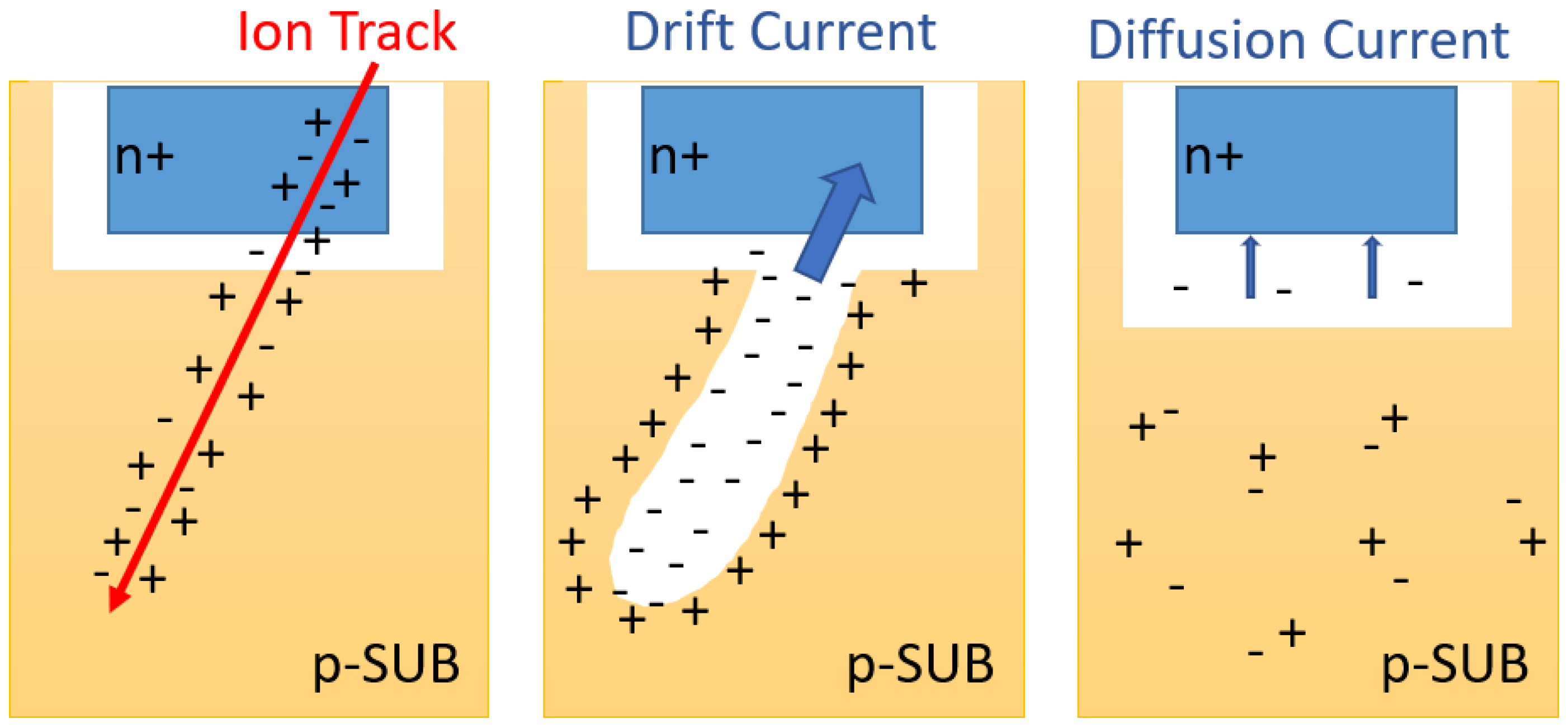
2.1. Single-Event Effects

Neutrons, alpha-particles, protons, and heavy ions can alter the normal behaviour of electronic devices. Indeed, the particle hit on silicon material releases energy that generates electron–hole pairs (e-h pairs). If an electrical field is present in the place where the ion strikes, a transient current is generated [17,18]. This phenomenon, called SEE, can affect the silicon devices in different manners depending on the place where they are generated. Indeed, the SEE can affect the normal behaviour of the system flipping bit in data management and transmission, leading to a permanent data error, called a single-event upset [13]. The SEE can also affect the clock signal, altering its phase and generating timing issues in synchronous systems. In addition, the current generated by the SEE can trigger pending latch-up with disruptive consequences (single-event latch-up) [19].
Figure 1 shows the basic principle of e-h pairs’ generation and collection in a p-n junction. The ion impacts on the silicon devices, generating e-h pairs (Figure 1, left), which are separated by the junction electric field (Figure 1, centre), generating the transient drift current. After a first current peak, the phenomenon is dominated by a diffusion current (Figure 1, right). The number of e-h pairs generated into a struck MOSFET depend on the linear energy transfer (LET) of the hitting particle and on the hit material. The shape and intensity of the current pulse generated by this phenomenon depend both on the number of e-h pairs generated as well as on the technology used (doping density, well depth, well shapes, materials).
This unwanted phenomenon that reduces the reliability of the electronics system is instead used for particle and photon detection. In this case, the e-h pairs’ generation is boosted using special material and/or the realisation of particular structures [20].
Although a technology computer-aided design considers all the phenomena produced by ionising particles with the p-n junction interaction, because the parameters strongly depend on the technology [21,22,23], the traditional double exponential law is used in simulation-before-test to model the shape of the transient current by using a double exponential current source in the design for the charge injection [24,25]. However, this model may not accurately represent certain SEEs [26,27], and for better results, this simulation can be performed with a dual double exponential current source, as reported in [28].

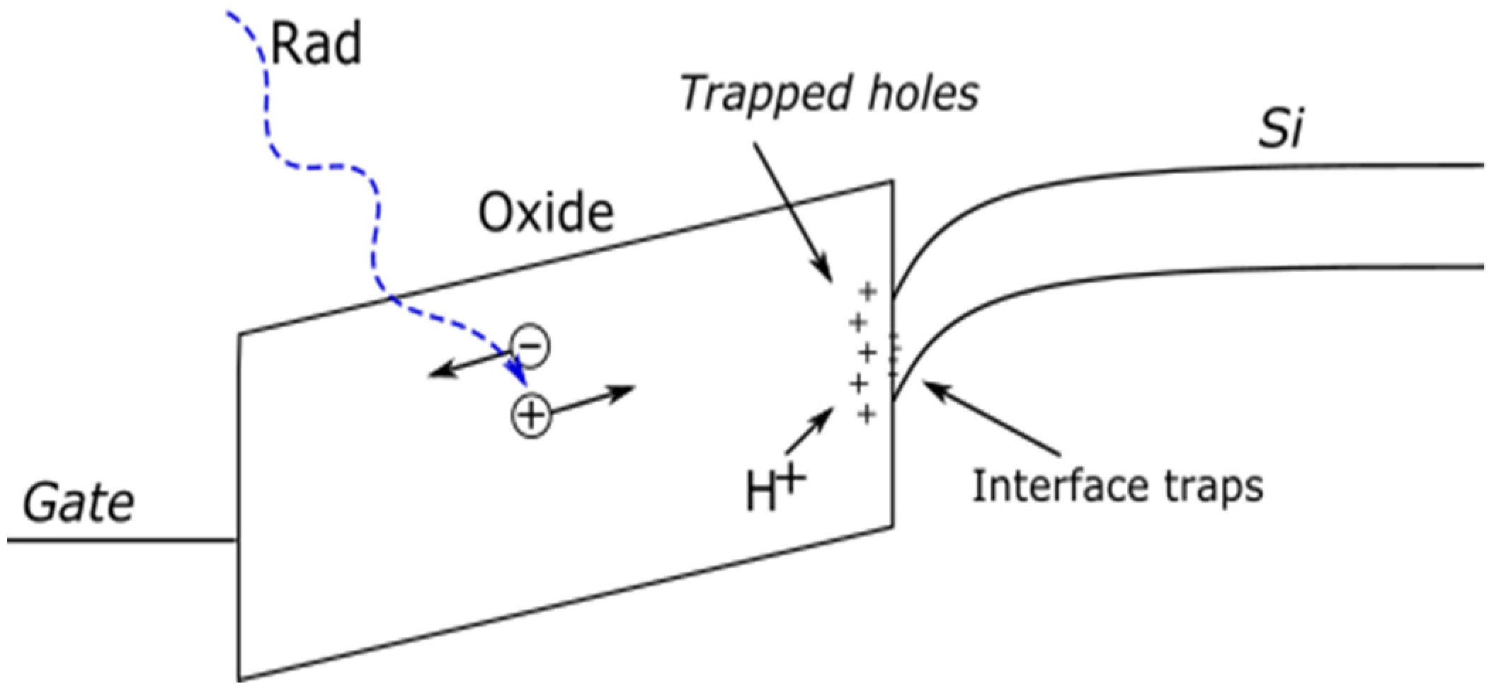
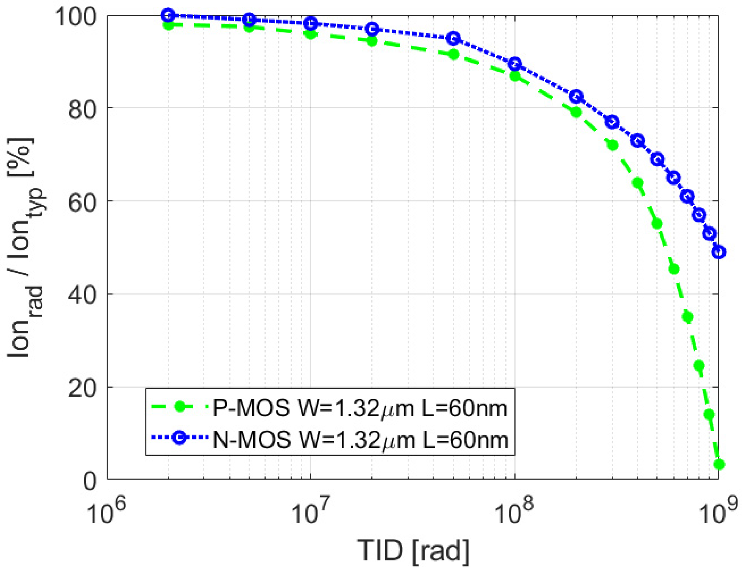
2.2. Total Ionising Dose Effects

Although an ionising particle can produce a temporary ionisation effect when it interacts with a p-n junction, a fixed ionisation effect may also occur when the e-h pairs are generated in the oxide insulators [29]. This effect could degrade the oxides’ lifetime or cause a gate rupture.
If the gate plate has a positive gate-substrate bias, most of the electrons generated in the oxide drift toward the gate plate because they are extremely mobile compared to the holes going toward the SiO2/Si interface, as shown in Figure 2. The positive charge accumulated at the silicon interface neutralizes the electron present in the p-substrate of an N-MOSFET and the threshold voltage is reduced. In addition, the increase of the electric field in the oxide increases the build-up of holes at the SiO2/Si interface. In a P-MOSFET device, the charge in the oxide is also positive and an increase in the threshold voltage occurs. Radiation-induced hole transport has a strong dependence on gate oxide thickness, as displayed in [30], in which the radiation hardening of the oxide decreases with tox2 law. The thinner the oxide, the harder the device.

3. TID and SEE in Simulation-before-Test

As described before, radiation hardening by shield offers an excellent level of radiation hardening, but it is usually expensive, and, on the other hand, radiation hardening by process requires a dedicated and expensive technology process that does not have the same maturity as the standard one.
Radiation hardening by design addresses the requirements of harsh environments, and it ensures to design complex integrated circuits (ICs) in a commercial technology without increasing production costs, but usually, an increase of silicon area and power consumption occurs. These mitigation techniques can be implemented at the circuit or system level, and simulation-before-tests increase the reliability of the fault diagnosis.

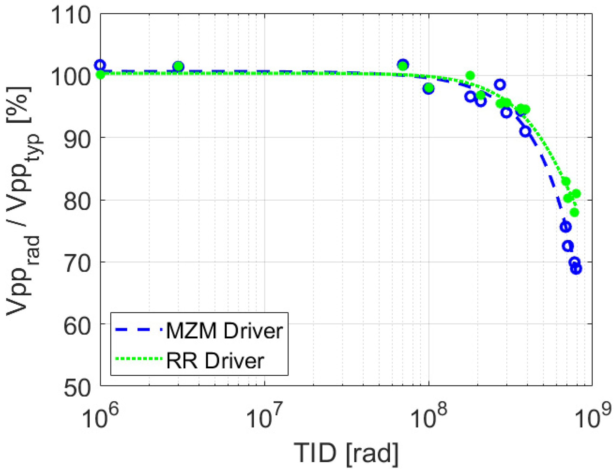
3.1. Drivers for Electro-Optical Modulators

The 65 nm technology is currently the state-of-the-art technology for radiation (rad)-hard applications due to its 2 nm thin gate oxide, which makes its devices very rad-hard. Nevertheless, the e-h pairs generated in the spacer oxide and at its interface with the LDD (lightly doped drain) region can modify the effective doping of LDD and affect the overall channel resistance. The effects of radiation on thick oxides are also shown in the shallow trench isolation between different devices, since the charge trapped in the lateral isolation oxide affects the transistor electric field.
Figure 3 shows the percentual variation of the on-current of minimum size MOSFETs connected in a diode configuration (the gate is connected to the drain) as a function of the TID. The experimental data are related to the 65 nm technology targeted in this work and are extracted from [31]. Since the minimum size devices have a higher cut-off frequency than the wider ones, high-speed applications are more oriented toward these devices. However, their performance is heavily influenced by the cumulated charge due to TID. As shown in Figure 3, N-MOSFET devices have an on-current reduction of about 50% at 1 Grad, and even worse is the impact on P-MOSFET devices with an on-current loss close to 100%. Obviously, with these levels of performance degradation, a classical device cannot operate near 1 Grad, making the development and adoption of RHBD techniques mandatory.
Today, in the literature, only a few 65 nm technology irradiation data of minimum size MOSFETs exposed up to 1 Grad are present [31,32,33,34,35]. In order to consider the impact of high-level TID in simulation-before-test to predict the system behaviour, device models for both the transistor types with different lengths and widths have to be created.
The models for N-MOSFETs and P-MOSFETs, exposed to high dose levels, are developed starting from literature data extracted from the same commercial-grade technology [31,32,33,34,35]. The MOSFETs’ properties, such as threshold voltage, offset voltage, electrical mobility, and subthreshold swing, are set in a BSIM (Berkeley Short-channel IGFET Model), taking into account different transistors’ widths and lengths.
For example, the data related to the threshold voltage variation for N-MOSFETs with minimum length (60 nm) and four widths (120, 240, 480 nm, and 1 µm) when exposed to 1 Grad are extracted from [32]. The dependence of the threshold voltage variation from the N-MOSFET length is extracted from [33], where 1 µm width N-MOSFETs with eight lengths (60, 120, 240, 360, 480, 800 nm, 1 µm, 10 µm) are exposed up to 1 Grad. Starting from this raw data, a function capable to fit the literature data as a function of MOSFET width and length is found. In particular, the coefficients of the multi-exponential polynomial, shown in Equation (1), that best fit the data are extracted:
y = C 1 + C 2 e x + C 3 x e x + C 4 x 2 e x + C 5 x 3 e x + C 6 log x + C 7 x log x + C 8 x 2 log x
This allows for obtaining the threshold voltage variation of N-MOSFETs exposed to 1 Grad with different lengths and widths. These functions are then introduced in the standard BSIM technology files provided by the foundry to model the devices exposed to 1 Grad. This procedure is performed for both device types (N-MOSFET and P-MOSFET) and for different parameters, such as threshold voltage, subthreshold swing, offset voltage, and electrical mobility. In particular, the data of the variation of the N-MOSFET threshold voltage up to 1 Grad are extracted from [31], while those for P-MOSFETs are extracted from the data in [34]. The variation of the offset voltage, for both MOSFET types, is extracted from [33]. The reduction of electrical mobility for both MOSFET types is extrapolated from the effects of the ON-current of MOSFETs exposed up to 1 Grad, for different transistor widths and lengths that are available in [33].
The device models are then verified by comparing ON-current vs. Vgs and Vds characteristics, obtained with DC simulations of the irradiated devices modelled with the characteristics reported in [31] and not used for the 1 Grad model building.
The model is based only on the few 65 nm technology irradiation data extracted from the literature. Therefore, the purpose of these DC models is to provide some first instruments, at simulation levels, to develop RHBD techniques for systems that must work in irradiated environments. A model improvement could be obtained by increasing the amount of data of MOSFETs exposed to 1 Grad.

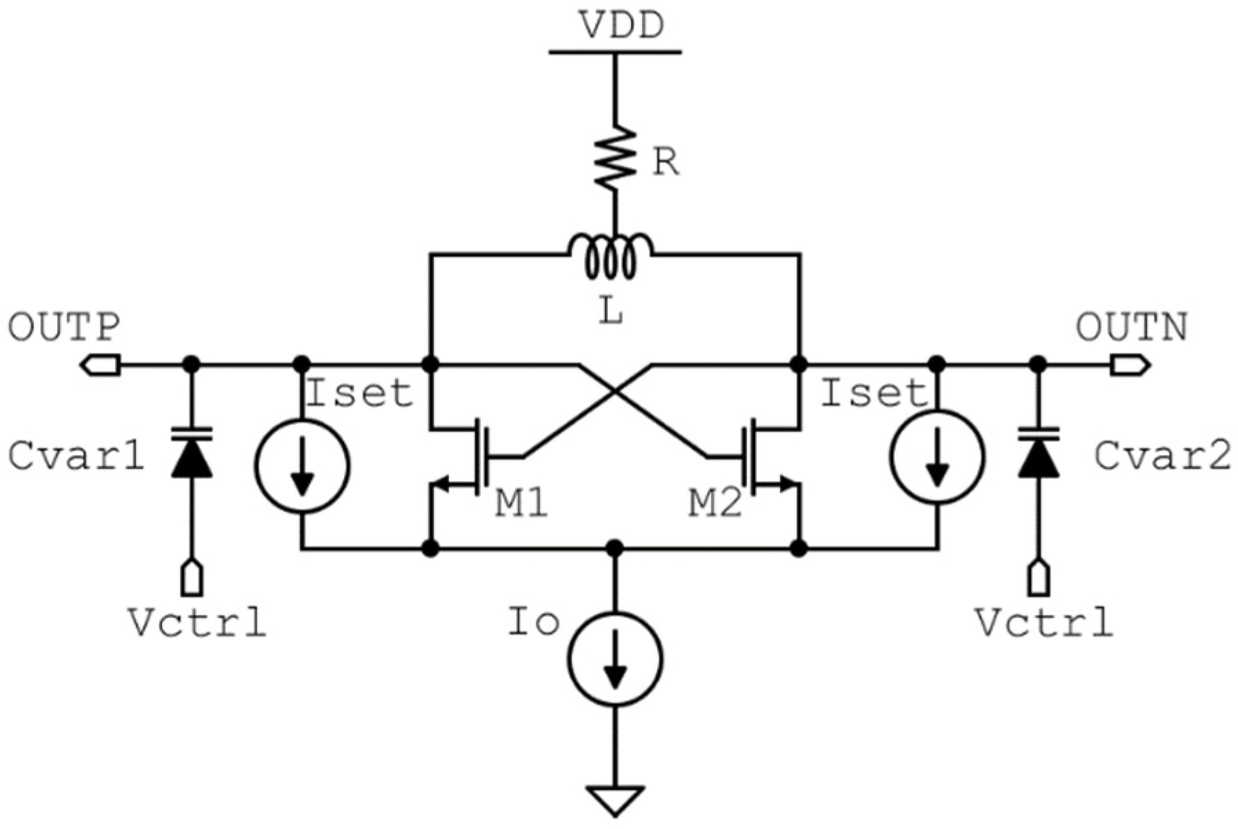
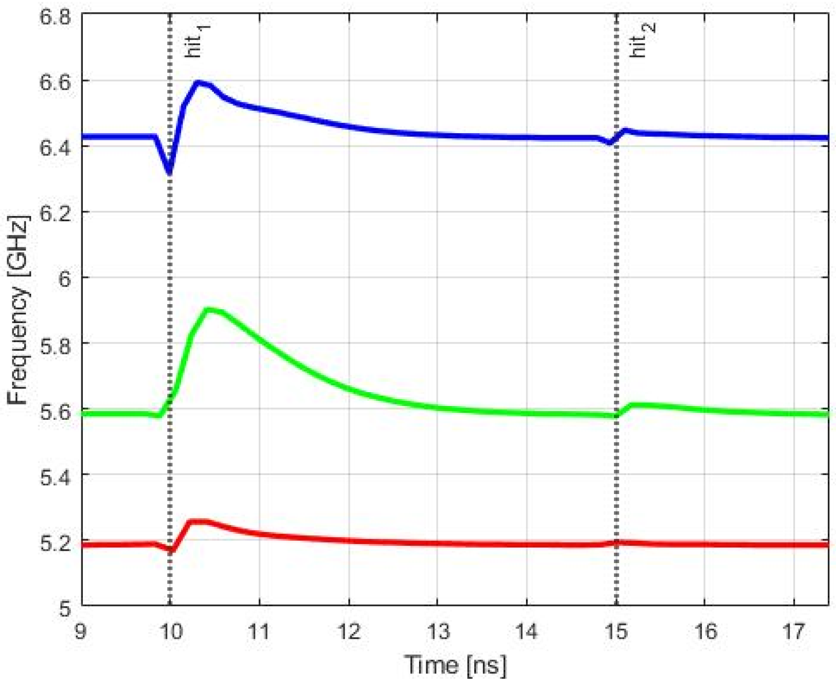
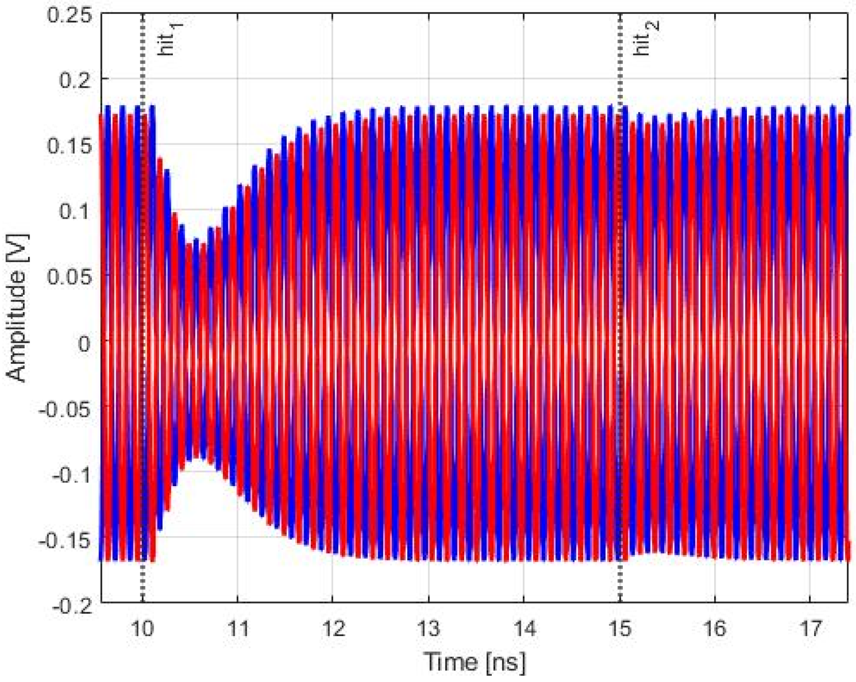
3.2. Voltage-Controlled Oscillator

In [36,37], an LC-Tank-based VCO compliant with the SpaceFibre protocol for the space environment is designed. The diagnosis of radiation effects is performed by a simulation-before-test, and the charge injection, due to particle hitting, is implemented with the classical double exponential shape [21,22,23]. For charge injection simulations, two assumptions were made: only one ionising particle hit the circuit at a time, and the probability that two consecutive ionising particles hit the same node is equal to zero.
The first-order model used for SEE simulations is shown in Equation (2), where tinj is the injection instant, ta is the collection time constant of the junction, tb is the ion track establishment time constant, and Q is the critical charge. Two sets of values are provided by IMEC: one for a particle with a LET of 5 MeV·cm2/mg and the other one with a LET of 60 MeV·cm2/mg. These set values are expressed for different time constants vs. critical charge (Q) and LET.
I SET = Q t a t b [ e t t i n j t a e t t i n j t b ]
This model is widely accepted by the scientific community for a first approximation, and the charge injection can be modelled by inserting a current pulse on each p-n junction, where the direction of the injected current depends on the device type. Moreover, the impact of the charge injection depends on signal status, thus the test bench should take it into account; once a sensitive node is found, it is necessary to investigate the different effects that an ionising particle has during waveform shape. For the implemented architecture, the most sensitive nodes are the outputs of the oscillator because varactors are directly connected to them [21,22,36,37], as shown in Figure 4.
Figure 5 and Figure 6 show the effects generated by a particle strike on the frequency of the most sensitive node of the VCO. When a VCO output node, which is the most sensitive, is hit, the released charge changes the voltage amplitude across varactors, creating a frequency deviation.
In Table 1, the data extracted from Figure 5 and Figure 6 are reported, in which the first three rows refer to the hit1 performed at 10 ns with the 60 MeV·cm2/mg ionising particle, and the last three rows refer to the hit2 performed at 15 ns with the 5 MeV·cm2/mg ionising particle. The second column shows the number of clock cycles in which the frequency assumes a different value due to the strike of an ionising particle.
Varactors have the gate plate fixed to the output common mode of VDD/2. To maximise TR [23,38], the control voltage explores the range from 0 V to VDD, even if varactors work in the accumulation region for a control voltage up to VDD/2, and then they work in the depletion region. When the control voltage assumes low values, varactors are more capacitive, less variation at the voltage node occurs, and a small frequency variation is achieved.

4. RHBD Mitigation Techniques

4.1. Drivers for Electro-Optical Modulators

Knowing the impact that different radiation effects have on single devices can provide information on the behaviour of more complex systems exposed to radiation. In [39], the development of high TID models, as shown in Section 3.1, has led to simulation-before-test for the design of 800 Mrad radiation-hard drivers for electro-optical modulators designed in Silicon Photonics technology. This has allowed to diagnosis the main source of faults and acts on the circuit design for their mitigation.
For example, one of the main effects that causes huge performance degradation in MOSFET performances is due to the charge collected in the shallow trench isolation. After the diagnosis of this issue, a countermeasure can be developed, such as the use of enclosed layout transistors that avoid the edge between the gate and the shallow trench isolation [39]. The designed model for different MOSFET lengths has allowed for understanding that the device performance degradation effect can be addressed using long transistors to reduce the channel percentage near the LDD. Obviously, the use of long MOSFETs impacts on the high-speed performance of the system that needs to be compensated. The previous effects have a heavier impact on P-MOSFET than the N-type one, as shown in Figure 3, therefore one of the stronger solutions adopted to address the high-level TID is the avoidance of P-MOSFETs adopting a CML (current mode technology) architecture composed only of N-MOSFETs and resistors. Moreover, considering the quadratic relationship between the radiation hardness of the device and the gate oxide thickness [30], only thin gate oxide devices could be used in the system architecture. In case of “high-voltage” applications, where the voltage exceeds the maximum voltage that thin gate oxide devices can sustain, new architecture solutions, such as totem-pole [38], have to be adopted to handle the “high-voltage” without using thick oxide devices.
The drivers designed in [39], one for a Mach Zehnder Modulator (MZM) and the other for a Ring Resonator (RR), adopting the previous RHBD techniques, are fabricated in 65 nm technology and exposed to X-rays to experimentally verify their radiation hardness. Without the use of the RHBD techniques, as previously described, a classic CMOS architecture with minimum size devices could be adopted for the drivers. In fact, the CMOS architecture has a lower power consumption than CML ones, since it does not have a static power consumption. In addition, the minimum size devices have a higher cut-off frequency than longer devices, increasing the drivers’ bandwidth and reducing the layout area. However, the poor radiation hardness shown in Figure 3 is expected with this solution, making it not useful for high TID levels. Instead, thanks to the RHBD techniques adopted, the drivers show greater radiation hardness.
Figure 7 reports the amplitude variation of the eye diagram of the output signals of both designed drivers as a function of TID levels. The diagnosis of the TID results shows a reduction in voltage amplitude of about 20–30% at 800 Mrad. At the same TID levels, Figure 3 shows a performance decrease of about 43% and 78% for N-type and P-type MOSFETs, respectively. In the case of CMOS architecture, the losses of the P-MOSFET devices would have dominated the system performance, with losses close to 80%. The nearly 10% difference in loss between the two drivers is due to the two different output stages’ pull-ups. Indeed, the MZM driver has an external resistive pull-up and the RR driver has an internal one. The impact of this pull-up can also be observed in the degradation of the fall and rise time. The driver with internal pull-up shows 40% greater rise time degradation than the driver with external pull-up. Therefore, an analysis of the impact that cumulated doses have on the silicon passive elements should be performed. However, no high-dose experiments on passive devices are reported in the literature.

4.2. Voltage-Controlled Oscillator

While for TID effects it is possible to extract a model, and the data can be used to perform an accurate fault diagnosis in a simulation-after-test, a simulation-before-test performed to simulate charge injection does not reveal all the mechanisms that could be present in an integrated circuit due to its complexity, and experimental measurements often reveal unforeseen mechanisms other than simple charge injection, that cannot be easily simulated during the design of the IC.
However, to mitigate the radiation effects in the VCO, only simulation-before-test can be performed with the use of RHBD techniques. In particular, all the active components were designed oversized compared to the minimum size that allows meeting the 6.25 GHz oscillation constraint to mitigate the impact of SEE on the VCO performance. Following the capacitance rule V = Q/C and assuming a constant amount of charge released by a particle hit, the higher the capacitance of a node, and the lower its voltage peak generated by the SEE. Therefore, MOSFETs in the cross-coupled cell were designed with the maximum number of fingers allowed by technology with an oversized value for the MOSFET width to increase parasitic capacitance and reduce voltage variations when an extra charge was injected in a p-n junction. Additionally, MOSFETs in the simple current mirror were designed as multi-finger devices with an oversized transistor width, but compatible with the maximum MOSFET length to reduce the gds parameter. This mitigation technique requires more area occupation and reduces the tuning range.

5. Conclusions

Commercial technology can be used to implement complex systems capable of working in harsh environments, and this paper presented the impact that radiation-induced fault diagnosis has on the design of mitigation techniques. The results obtained with the RHBD to address the radiation problem lead the two different architectures to work properly at the radiation level required by the two applications, and this will increase the radiation level addressable by devices operating in harsh environments.
In particular, the devices designed for the two case studies presented in this paper mainly require dealing with two different radiation effects. The devices operating in high-energy physics experiments (such as the LHC) have to face extremely high levels of total dose. In contrast, the devices operating in space environments have to address issues more related to single-event effects. By predicting the different types of failures with simulation-before-test, appropriate countermeasures can be taken. For this, the development of models to simulate the response of silicon devices to different radiation phenomena is fundamental. Therefore, in this work, models based on experimental data from the literature were developed for the analysis of TID effects and SEE. These models enabled the development of strategies for designing TID and SEE countermeasures.
TID effects on commercial-grade CMOS technology can be addressed by avoiding the use of thick oxide devices, preferring the use of stacked architectures for high-voltage handling. Considering the different cumulative dose impacts on P-type and N-type MOSFETs (see Figure 3), the first one should be avoided in the design of devices operating at high dose levels, especially for high-speed applications. The use of long MOSFETs helps to reduce the effect of the charge stored in the spacers, but on the other hand, limits the device cut-off frequency. Therefore, radiation phenomena are particularly enhanced in high-frequency, high-speed applications. These RHBD techniques are used in the design of high-speed drivers for electro-optical modulators, and their impacts have been experimentally verified with X-ray exposure and reported in Figure 7, showing a 50–60% improvement in radiation hardness thanks to the implemented techniques.
The double exponential model used to simulate the current injected during a SEE allowed analysing, with simulation-before-test, the consequences that a SEE can have on a silicon device. The practical example of a VCO designed in 65 nm is reported to highlight the importance of SEE modelling during the system design phase. In fact, thanks to the SEE simulation, it was possible to identify the circuit nodes most sensitive to particle impact and act on them to improve the radiation tolerance of the system. Moreover, the simulations showed that the control voltage has a direct impact on the frequency shift due to SEE. Therefore, the VCO operating in radiation-pervaded environments should be designed at a higher frequency than the target one and then trimmed by reducing the control voltage. The impact on device performance of different particle energies was also shown to highlight that RHBD techniques can be balanced according to the particle energies expected in the environment in which the device is to operate.
Thanks to the mitigation techniques implemented and to simulations before and after testing, it is possible to design integrated circuits capable of working in harsh environments, such as space and high-energy physics, without increasing manufacturing costs.

Author Contributions

D.M.: investigation, methodology, conceptualisation, writing—review and editing; G.C.: investigation, methodology, conceptualisation, software, writing—review and editing; S.S.: writing—review and editing. All authors contributed to the present paper with the same effort in finding available literature resources, conducting simulations, as well as writing the paper. All authors have read and agreed to the published version of the manuscript.

Funding

This work was supported by PHOS4BRAIN and ISHTAR Projects by INFN and the University of Pisa, as well as by the Dipartimento di Eccellenza Crosslab project by MIUR.

Conflicts of Interest

The authors declare no conflict of interest.

References

  1. Sinclair, D.; Dyer, J. Radiation Effects and COTS Parts in SmallSats. In Proceedings of the 27th Annual AIAA/USU Conference on Small Satellites, Logan, UT, USA, 10−15 August 2013; paper SSC13-IV. pp. 1–12. [Google Scholar]
  2. Binu, D.; Kariyappa, B. A survey on fault diagnosis of analog circuits: Taxonomy and state of the art. AEU Int. J. Electron. Commun. 2017, 73, 68–83. [Google Scholar] [CrossRef]
  3. Luyue, L.; Kehong, L.; Guanjun, L.; Jing, Q. Intelligent Diagnosis Method for Intermittent Fault of Digital Circuit Based on Dynamic Power Current. In Proceedings of the 2021 6th International Conference on Intelligent Computing and Signal Processing (ICSP), Xi’an, China, 9−11 April 2021; pp. 786–791. [Google Scholar] [CrossRef]
  4. Tadeusiewicz, M.; Halgas, S. A Method for Local Parametric Fault Diagnosis of a Broad Class of Analog Integrated Circuits. IEEE Trans. Instrum. Meas. 2017, 67, 328–337. [Google Scholar] [CrossRef]
  5. Tian, S.; Yang, C.; Chen, F.; Liu, Z. Circle Equation-Based Fault Modeling Method for Linear Analog Circuits. IEEE Trans. Instrum. Meas. 2014, 63, 2145–2159. [Google Scholar] [CrossRef]
  6. Grasso, F.; Luchetta, A.; Manetti, S.; Piccirilli, M.C. Symbolic techniques in neural network based fault diagnosis of analog circuits. In Proceedings of the 2010 XIth International Workshop on Symbolic and Numerical Methods, Modeling and Applications to Circuit Design (SM2ACD), Gammarth, Tunisia, 4–6 October 2010; pp. 1–4. [Google Scholar] [CrossRef]
  7. Roche, P.; Gasiot, G.; Autran, J.L.; Munteanu, D.; Reed, R.A.; Weller, R.A. Application of the TIARA Radiation Transport Tool to Single Event Effects Simulation. IEEE Trans. Nucl. Sci. 2014, 61, 1498–1500. [Google Scholar] [CrossRef]
  8. Reed, R.A.; Weller, R.A.; Mendenhall, M.; Fleetwood, D.M.; Warren, K.M.; Sierawski, B.D.; King, M.P.; Schrimpf, R.D.; Auden, E.C. Physical Processes and Applications of the Monte Carlo Radiative Energy Deposition (MRED) Code. IEEE Trans. Nucl. Sci. 2015, 62, 1441–1461. [Google Scholar] [CrossRef]
  9. Uznanski, S.; Gasiot, G.; Roche, P.; Semikh, S.; Autran, J.-L. Combining GEANT4 and TIARA for Neutron Soft Error-Rate Prediction of 65 nm Flip-Flops. IEEE Trans. Nucl. Sci. 2011, 58, 2599–2606. [Google Scholar] [CrossRef]
  10. Hubert, G.; Bourdarie, S.; Artola, L.; Duzellier, S.; Roussel, J.-F. Multi-scale modeling to investigate the single event effects for space missions. Acta Astronaut. 2011, 69, 526–536. [Google Scholar] [CrossRef]
  11. European Cooperation for Space Standardization, SpaceFibre Standard, ECSS-E-ST-50-11C-DIR1. 2019. Available online: http://ecss.nl/standard/ecss-e-st-50-11c-dir1 (accessed on 1 September 2021).
  12. Haddad, N.F.; Kelly, A.T.; Lawrence, R.K.; Li, B.; Rodgers, J.C.; Ross, J.F.; Warren, K.M.; Weller, R.A.; Mendenhall, M.H.; Reed, R.A. Incremental Enhancement of SEU Hardened 90 nm CMOS Memory Cell. IEEE Trans. Nucl. Sci. 2011, 58, 975–980. [Google Scholar] [CrossRef]
  13. Clark, L.T.; Mohr, K.C.; Holbert, K.E.; Yao, X.; Knudsen, J.; Shah, H. Optimizing Radiation Hard by Design SRAM Cells. IEEE Trans. Nucl. Sci. 2007, 54, 2028–2036. [Google Scholar] [CrossRef]
  14. Lv, H.; Sun, Y.; Li, P.; Luo, L.; Zhang, H.; Yu, Q.; Tang, M. Research on optimization design of radiation dose shield hardening for aerospace components. In Proceedings of the 2017 Prognostics and System Health Management Conference (PHM-Harbin), Harbin, China, 9–12 July 2017; pp. 1–5. [Google Scholar] [CrossRef]
  15. Kim, S.; Lee, J.; Kwon, I.; Jeon, D. 2020. TID-tolerant inverter designs for radiation-hardened digital systems. Nucl. Instrum. Methods Phys. Res. Sect. A Accel. Spectrometers Detect. Assoc. Equip. 2020, 954, 161473. [Google Scholar] [CrossRef]
  16. Jeon, H.; Kwon, I.; Je, M. Radiation-Hardened Sensor Interface Circuit for Monitoring Severe Accidents in Nuclear Power Plants. IEEE Trans. Nucl. Sci. 2020, 67, 1738–1745. [Google Scholar] [CrossRef]
  17. Dodd, P.; Massengill, L. Basic mechanisms and modeling of single-event upset in digital microelectronics. IEEE Trans. Nucl. Sci. 2003, 50, 583–602. [Google Scholar] [CrossRef]
  18. Andrews, J.L.; Schroeder, J.E.; Gingerich, B.L.; Kolasinski, W.A.; Koga, R.; Diehl, S.E. Single Event Error Immune CMOS RAM. IEEE Trans. Nucl. Sci. 1982, 29, 2040–2043. [Google Scholar] [CrossRef]
  19. Johnston, A.H. The influence of VLSI technology evolution on radiation induced latchup in space systems. IEEE Trans. Nucl. Sci. 1996, 43, 505–521. [Google Scholar] [CrossRef]
  20. Taghinejad, M.; Taghinejad, H.; Ganji, M.; Rostamian, A.; Mohajerzadeh, S.; Abdolahad, M.; Kolahdouz, M. Integration of Ni2Si/Si Nanograss Heterojunction on n-MOSFET to Realize High-Sensitivity Phototransistors. IEEE Trans. Electron Devices 2014, 61, 3239–3244. [Google Scholar] [CrossRef]
  21. Rathore, P.; Nakhate, S. Development of Radiation Hardened by Design (RHBD) of NAND gate to mitigate the effects of single event transients (SET). In Proceedings of the IEEE 1st International Conference on Power Electronics, Intelligent Control and Energy Systems (ICPEICES), Delhi, India, 4–6 July 2016; pp. 1–6. [Google Scholar] [CrossRef]
  22. Bkeller, B.K. Project UPSET: Under-Standing and Protecting against Single Event Transients. Available online: https://www.semanticscholar.org/paper/Project-UPSET-%3A-Understanding-and-Protecting-Single-bkeller/ee76ac31beefd6dacf6e094656c5b603a09ce762 (accessed on 1 September 2021).
  23. Wirth, G.I.; Vieira, M.G.; Neto, E.H.; Kastensmidt, F.L. Modeling the sensitivity of CMOS circuits to radiation induced single event transients. Microelectron. Reliab. 2008, 48, 29–36. [Google Scholar] [CrossRef]
  24. Wrobel, F.; DiLillo, L.; Touboul, A.D.; Pouget, V.; Saigne, F. Determining Realistic Parameters for the Double Exponential Law that Models Transient Current Pulses. IEEE Trans. Nucl. Sci. 2014, 61, 1813–1818. [Google Scholar] [CrossRef]
  25. Heijmen, T.; Giot, D.; Roche, P. Factors That Impact the Critical Charge of Memory Elements. In Proceedings of the 12th IEEE International On-Line Testing Symposium (IOLTS’06), Como, Italy, 10–12 July 2006; pp. 57–62. [Google Scholar] [CrossRef]
  26. Loveless, T.D.; Kauppila, J.S.; Jagannathan, S.; Ball, D.R.; Rowe, J.D.; Gaspard, N.J.; Atkinson, N.M.; Blaine, R.W.; Reece, T.R.; Ahlbin, J.R.; et al. On-Chip Measurement of Single-Event Transients in a 45 nm Silicon-on-Insulator Technology. IEEE Trans. Nucl. Sci. 2012, 59, 2748–2755. [Google Scholar] [CrossRef]
  27. Dasgupta, S.; Witulski, A.F.; Bhuva, B.L.; Alles, M.L.; Reed, R.A.; Amusan, O.A.; Ahlbin, J.R.; Schrimpf, R.; Massengill, L.W. Effect of Well and Substrate Potential Modulation on Single Event Pulse Shape in Deep Submicron CMOS. IEEE Trans. Nucl. Sci. 2007, 54, 2407–2412. [Google Scholar] [CrossRef]
  28. Black, D.A.; Robinson, W.H.; Wilcox, I.Z.; Limbrick, D.B.; Black, J.D. Modeling of Single Event Transients With Dual Double-Exponential Current Sources: Implications for Logic Cell Characterization. IEEE Trans. Nucl. Sci. 2015, 62, 1540–1549. [Google Scholar] [CrossRef]
  29. Lee, C.; Cho, G.; Unruh, T.; Hur, S.; Kwon, I. Integrated Circuit Design for Radiation-Hardened Charge-Sensitive Amplifier Survived up to 2 Mrad. Sensors 2020, 20, 2765. [Google Scholar] [CrossRef]
  30. Saks, N.S.; Ancona, M.G.; Modolo, J.A. Radiation Effects in MOS Capacitors with Very Thin Oxides at 80degK. IEEE Trans. Nucl. Sci. 1984, 31, 1249–1255. [Google Scholar] [CrossRef]
  31. Ding, L.; Gerardin, S.; Bagatin, M.; Mattiazzo, S.; Bisello, D.; Paccagnella, A. Drain Current Collapse in 65 nm pMOS Transistors After Exposure to Grad Dose. IEEE Trans. Nucl. Sci. 2015, 62, 2899–2905. [Google Scholar] [CrossRef]
  32. Faccio, F.; Michelis, S.; Cornale, D.; Paccagnella, A.; Gerardin, S. Radiation-Induced Short Channel (RISCE) and Narrow Channel (RINCE) Effects in 65 and 130 nm MOSFETs. IEEE Trans. Nucl. Sci. 2015, 62, 2933–2940. [Google Scholar] [CrossRef]
  33. Faccio, F.; Borghello, G.; Lerario, E.; Fleetwood, D.M.; Schrimpf, R.D.; Gong, H.; Zhang, E.X.; Wang, P.; Michelis, S.; Gerardin, S.; et al. Influence of LDD Spacers and H+Transport on the Total-Ionizing-Dose Response of 65-nm MOSFETs Irradiated to Ultrahigh Doses. IEEE Trans. Nucl. Sci. 2017, 65, 164–174. [Google Scholar] [CrossRef]
  34. Menouni, M.; Barbero, M.; Bompard, F.; Bonacini, S.; Fougeron, D.; Gaglione, R.; Rozanov, A.; Valério, P.; Wang, A. 1-Grad total dose evaluation of 65 nm CMOS technology for the HL-LHC upgrades. J. Instrum. 2015, 10, C05009. [Google Scholar] [CrossRef] [Green Version]
  35. Ciarpi, G.; Saponara, S.; Magazzù, G.; Palla, F. Radiation Hardness by Design Techniques for 1 Grad TID Rad-Hard Systems in 65 nm Standard CMOS Technologies. In International Conference on Applications in Electronics Pervading Industry, Environment and Society; Springer: Cham, Switzerland, 2018; pp. 269–276. [Google Scholar] [CrossRef]
  36. Monda, D.; Ciarpi, G.; Saponara, S. Analysis and Comparison of Rad-Hard Ring and LC-Tank Controlled Oscillators in 65 nm for SpaceFibre Applications. Sensors 2020, 20, 4612. [Google Scholar] [CrossRef] [PubMed]
  37. Monda, D.; Ciarpi, G.; Saponara, S. Design and Verification of a 6.25 GHz LC-Tank VCO integrated in 65 nm CMOS Technology Operating up to 1 Grad TID. IEEE Trans. Nucl. Sci. 2021. [Google Scholar] [CrossRef]
  38. Razavi, B. RF Microelectronics; Prentice Hall: Hoboken, NJ, USA, 1998; Volume 1. [Google Scholar]
  39. Ciarpi, G.; Magazzù, G.; Palla, F.; Saponara, S. Design, implementation, and experimental verification of 5 Gbps, 800 Mrad TID and SEU-tolerant optical modulators drivers. IEEE Trans. Circuits Syst. I Regul. Pap. 2019, 67, 829–838. [Google Scholar] [CrossRef]
Figure 1. This figure shows the phases of an ion strike on a p-n junction. (left) The ion generates e-h pairs, releasing its energy. (centre) The electron and holes are generated, and a drift current is observed. (right) The diffusion current dominates the phenomena.
Electronics 10 02144 g001
Figure 2. N-MOSFET energy bands diagram with gate-substrate biased to positive voltage.
Electronics 10 02144 g002
Figure 3. Percentual variation of the on-current of minimum size MOSFETs connected as a diode (the gate is connected to the drain) as a function of TID.
Electronics 10 02144 g003
Figure 4. Schematic circuit level of the controlled oscillator with the double exponential current sources connected at the outputs.
Electronics 10 02144 g004
Figure 5. Effect on the VCO free-running frequency, of two different particles’ hits. The two hit instants, hit1 and hit2, correspond to particle energy of 60 and 5 MeV·cm2/mg, respectively. The effects with three different values of the control voltage are also reported: 0 V (red Line), VDD/2 (green line), and VDD (blue line).
Electronics 10 02144 g005
Figure 6. Differential output amplitude of the oscillator vs. time hit by an ionising particle plotted for the control voltage value equal to VDD. Two different sets of values were used: ionising particles with 60 and 5 MeV·cm2/mg at 10 and 15 ns, respectively.
Electronics 10 02144 g006
Figure 7. Degradation of the output voltage eye diagram amplitude as a function of TID for the two drivers. The points represent the performed measurements for different TID levels, and the dotted-dashed lines are their trend curves.
Electronics 10 02144 g007
Table 1. Frequency and amplitude variations due to SEE.
Control VoltageClock CyclesFrequency VariationsAmplitude Variations
hit10151.24%43.8%
VDD/2265.58%48.82%
VDD242.45%57.49%
hit2060.11%1.55%
VDD/2120.5%3.85%
VDD130.46%3.17%
Publisher’s Note: MDPI stays neutral with regard to jurisdictional claims in published maps and institutional affiliations.

