
GaAs-Based Serial-Input-Parallel-Output Interfaces for Microwave Core-Chips


Department of Electronics and Telecommunications, Politecnico di Torino, 10129 Turin, Italy
*
Author to whom correspondence should be addressed.
Electronics 2021, 10(23), 3029; https://0-doi-org.brum.beds.ac.uk/10.3390/electronics10233029
Submission received: 9 November 2021
/
Revised: 29 November 2021
/
Accepted: 2 December 2021
/
Published: 4 December 2021
(This article belongs to the Special Issue Microwave Integrated Core-Chips)
Abstract
:Microwave core-chips are highly integrated MMICs that are in charge of all the beam-shaping functions of a transmit-receive module within a phased array system. Such chips include switches, amplifiers and attenuators, phase shifters, and possibly other elements, each to be controlled by external digital signals. Given the large number of control lines to be integrated in a core-chip, the embedding of a serial to parallel interface is indispensable. Digital design in compound semiconductor technology is still rather challenging due to the absence of complementary devices and the availability of a limited number of metallization layers. Moreover, in large arrays, high chip yield and repeatability are required. This paper discusses and compares challenges and solutions for the key sub-circuits of GaAs serial to parallel converters for core-chip applications, reviewing the pros and cons of the different implementations proposed in the literature.
1. Introduction
Active electronically scanned Array (AESA) antennas allow for controlling the beam shape and direction without physically moving the antenna since phase and amplitude of the signals driving each radiating element are independently set through a dedicated transmit-receive module (TRM), digitally controlled by a central processor.
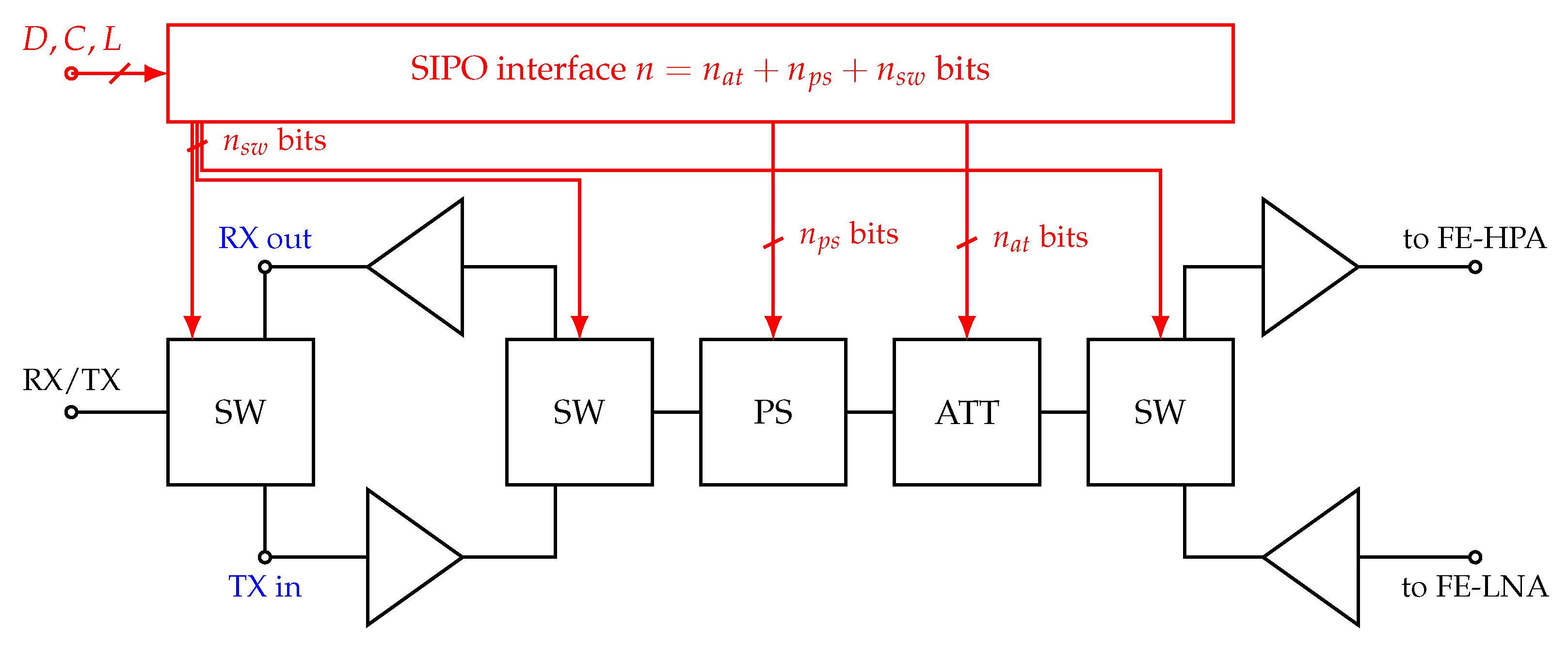
The core-chip (CC) is a mixed-signal highly-integrated multi-function MMIC performing all the core controlling functions of a TRM, i.e., path setting, phase shifting, amplitude control, together with low-level amplification at microwave frequencies from S- to Ka-band [1,2,3,4], while the high-level amplification functionalities are typically entrusted to a second dedicated MMIC, the front-end (FE), nowadays typically implemented in GaN technology [5,6]. To achieve accurate beam control, the number of control lines required within a CC can be very high, in the order of tens, and may thus represent a major issue in large AESA systems. Embedding a clocked synchronized serial-input-parallel-output (SIPO) interface in the CC drastically reduces the number of external pins required to control multiple internal bits, as it can control all the high frequency analog parts (switches, phase shifters and attenuators), with just few input lines, as shown in Figure 1. The large number of transistors required in logic circuits, make the SIPO interface one of the most critical blocks in a CC in terms of yield [7]. Beyond yield, current consumption, which impacts on chip self-heating and reliability [8], and chip area occupation are also crucial aspects to be optimized, together with digital noise margins, commutation speed and compatibility with the external logic levels, which are further key features that need to be taken into account for the design of the digital interface.
When dealing with digital electronics systems, the highest process maturity is provided by Silicon technology, well-established and worldwide adopted for all kinds of low/medium frequency digital applications. High-frequency Si-based processes, RF-CMOS and SiGe BiCMOS, provide easier implementation of digital circuits, thanks to the availability of complementary devices and a large number of metallization layers, and have advantages in terms of noise margins, cost and yield over GaAs-based technologies [9,10,11,12]. However, for the same device periphery, GaAs transistors can achieve higher commutation speed than Si ones and at a lower power [9,13,14]. This makes GaAs an appealing alternative to Si for high-speed logic circuits, especially when considering Enhancement/Depletion-mode (E/D-mode) technologies offering much more flexibility than D-mode-only processes for digital design. Moreover, GaAs technology ensures radiation hardness, a key feature for space and military applications, and, most important, its RF performance, both in terms of noise figure and output power capability, is still sensibly higher than that of Si technologies, which makes it the preferable choice for mixed digital/RF chips, like microwave core-chips.
This paper discusses and compares GaAs SIPO architectures found in the literature, evaluating advantages and disadvantages of the different logic families and architectures adopted. Section 2 describes the use of the SIPO interfaces in microwave core-chips, summarizing the state-of-the-art, while in the rest of the paper the different building blocks are detailed and discussed. After recalling the overall SIPO architecture in Section 3, GaAs logic families are presented. Then interface and memory elements are illustrated in Section 5 and Section 6, respectively, while Section 7 concludes and summarizes the work.
2. Literature Overview of SIPO Interfaces in GaAs Microwave Core-Chips
As shown in Figure 1, a microwave core-chip always includes an -bit variable attenuator and an -bit variable phase shifter. The higher the number of control bits, the finer the tuning of the signal amplitude and phase, and hence the higher the accuracy of the beam control, but this also increases the number of signals required to control these circuits. Moreover, one or more switches are often included to share the circuitry between the transmit and/or receive path or to include/exclude amplification stages, requiring additional control bits. The routing of the input control lines for each core-chip within an AESA system would rapidly become unsustainably complex increasing the number of bits, therefore embedding a serial-input-parallel-output interface represents a crucial benefit, where not a mandatory requirement, of microwave core-chips.
The state-of-the-art overview is reported in Table 1. Along with the number of bits, the designation of the bits within the core-chip is reported, when available: clearly, most of the bits are used for the phase and amplitude control, while, depending on the chip functionalities, up to six bits [15] are adopted for the switches. It is worth to note than in several cases [16,17,18,19] a serial output bit is also available, allowing to connect more CCs in daisy chain and configure them sequentially, and/or to test/monitor the SIPO output. In principle, it is sufficient to route the last bit to an output pad, possibly after level shifting/buffering as in [17]. Even if practically negligible, this represents a slight alteration in the load of the last bit with respect to all other bits, therefore in [18] an extra bit is included to be used specifically for the data output line. In [20] the number of SIPO bits is double than necessary so as to simultaneously load two different control words, containing, respectively, the receive- and transmit-mode CC configuration and stored in the even and off SIPO bits. Twelve multiplexers are then used to selectively send to the attenuator and phase shifter the proper word according to the CC operating mode which is given though an additional external input. This solution is particularly interesting when the CC is expected to be operated continuously switching between the two operating modes without changing the beam characteristics.
The most typical logic family adopted is the direct coupled FET logic (DCFL), requiring Enhancement-mode (E-mode) transistors. As detailed in Section 4, this solution ensures compactness, low device count and hence potentially high yield and low power consumption, especially in the E-mode-only version. The super buffered FET logic (SBFL) has been also proposed, which favors instead noise margins and achieves moderate speed, comparable to DCFL. The buffered FET logic (BFL) is the preferred choice when depletion-mode (D-mode) transistors are only available, or when they are deliberately exploited either to enhance speed or to allow higher RF operating frequencies for the analog portion of the CC [28,32]. Only two flip-flop architectures are present in the literature, which will be discussed in Section 6, even if in many works such a detail is not available, as well as the clock speed. The latter indeed is not a stringent design constraint, and is thus typically in the range of tens of megahertz, except for [32] where a simultaed bit rate of 3 Gbit/s is reported.
3. Circuit Architecture
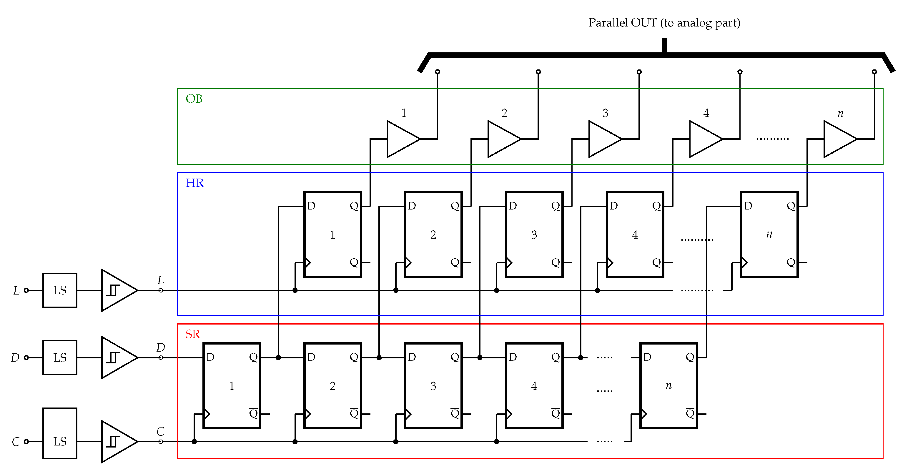
The block diagram of an n-bit SIPO interface is shown in Figure 2. It is composed of an n-bit shift register (SR) coupled with an n-bit hold register (HR), typically completed by n output buffers (OB), input level shifters (LS) for voltage level compatibility among different logic families and Schmitt trigger input buffers. The minimum number of inputs is 3, namely data (D), clock (C) and load (L) signals, as shown also in Figure 1. The shift register is loaded one bit at a time (serial input) according to the clock signal. After n clock cycles the entire CC configuration word is available (parallel output), and, upon reception of the load command, the HR samples in parallel all n output bits of the SR and stores them until a new load command is received. Clearly, the minimum time between two consecutive CC re-configuration is n clock cycles, but typically the frequency at which the CC needs to be re-configured is much lower, thus the HR remains most of the time in a hold state. Moreover, the HR does not interface with the external environment, but it is internally driven by the SR, i.e., by already synchronized signals, thus the probability of spurious commutations and/or synchronization issues is extremely low, which allows to simplify the HR architecture. This practically relaxes the switching speed and consumption requirements for this component with respect to the SR, which is thus the dominant sub-circuit in determining the overall SIPO interface performance. Finally, an array of output buffers takes care of adjusting the signals’ voltage level and driving capability.
Apart from the input interface, the rest of the SIPO circuit can be seen as n replicas of a basic building blocks made by one bit of the SR, one bit of the HR and one output buffer. When designing such basic bit-wise block, it is important to optimize the layout for compactness and modularity, to save costs and to make the structure easily extendable to an arbitrary number of bits [21,25]. An n-bit shift register is composed of n D-type flip-flops (DFFs) connected in daisy-chain arrangement and controlled by the same clock signal. In principle, the SR is operating all the time, however, in practice, some SR-shut-down procedures can be included. The simplest one is to suspend the clock signal when unnecessary, thus disabling bit-shifting regardless of the input data signal. This can be done externally or at CC-level through a dedicated input signal in AND with the clock input, as in [18]. To enhance noise immunity, lowering the probability of spurious transitions, the data line can be also suspended/disconnected in absence of the clock signal. Moreover, a dedicated power grid can be adopted for the SR, which allows switching off the SR when unused as in [28]. Since the SR is the core element of the SIPO interface, the DFFs play a crucial role in determining its power consumption, latency and size. All these parameters are interdependent, thus achieving the best trade-off among them is a main design challenge and the most suitable implementation depends on the case, based on which one of these features has to be favored. Most of the SIPO examples available in the literature adopt the same DFFs for the SR and the HR [20,24,25,27,29,31,32]. This choice is surely the most convenient in terms of design effort and modularity, since, once the DFF cell is optimized, it is just replicated times to create the two n-bit registers. However, in order to reduce the overall transistor count, hence reducing chip area occupation and improving yield, the HR can be implemented with simple D-type latches in place of flip-flops as in [15,19,28]. Since latches are sensitive to levels rather than transitions, in order to adopt this solution the load command must be given in the form of a short enable pulse rather than a transition as discussed in Section 6.
4. GaAs-Based Logic Gates
Gallium arsenide transistors are characterized by a Schottky barrier, which leads to forward gate conduction and voltage clamping and thus to a reduced voltage swing compared to silicon-based MOS technology. This in turn implies worse noise margins and the need of more complicated circuits aimed at avoiding the detrimental effect of gate conduction, also considering lack of complementary (p-type) devices, due to the large disproportion between hole and electron mobility. On the other hand, the larger transconductance, higher electron velocity and lower parasitic capacitances of GaAs FETs with respect to MOSFETs, allow for higher speed and higher drive currents at lower voltage, with an overall lower power consumption [9,14].
Many GaAs-based logic families have been developed since the early 80s when D- and then E-mode MESFET technologies became mature enough to provide acceptable yields [33], as listed in Table 2.
Early logic families were based exclusively on D-mode FETs (normally-ON devices), however, the high power consumption of even the simplest gate makes them hardly usable for developing complex structure as a SIPO interface. The availability of E/D-mode processes represented a breakthrough for the integration of digital architectures in GaAs core-chips, and are nowadays the preferred choice as can be noted from Table 1. Despite the lower knee voltage and hence lower power consumption of E-mode transistors [23], E/D processes are still limited with respect to depletion-only ones in terms of frequency and power density [28], which makes desirable the development of low-power D-mode logic circuits for very high frequency applications.
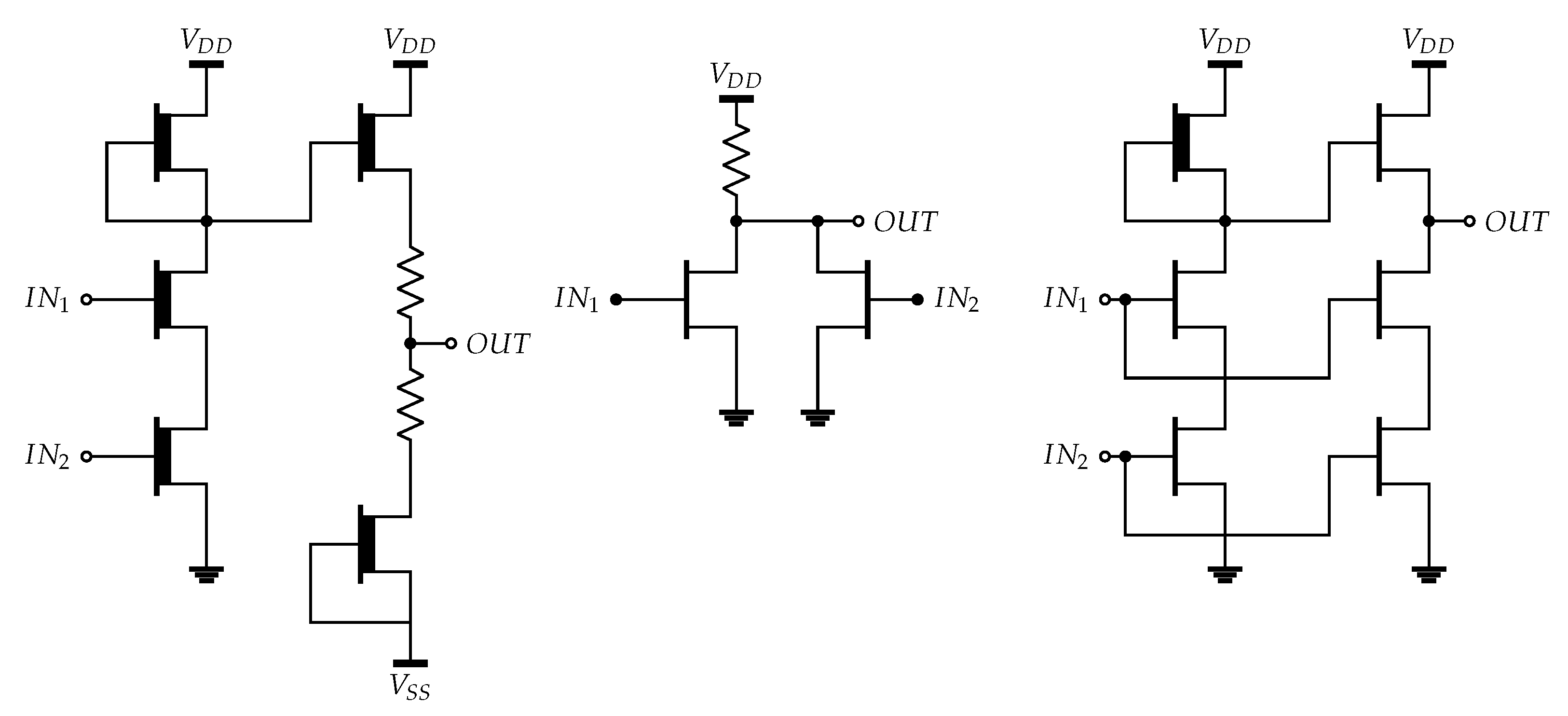
When only D-mode transistors are available, the buffered FET logic (BFL) is the preferred implementation thanks to the better noise margins and sensibly increased fan-out capability with respect to UFL and SDFL, and the higher frequency achievable with respect to capacitor-based families. As shown in Figure 3a, reporting the basic inverter (NOT) gate, each logic gate is loaded with a buffer stage (source follower, level-shifting diodes and pull-down transistor) increasing the current driving capability of the gate and performing the necessary level shifting required to drive the next stage, which needs a negative input voltage swing from , corresponding to a logic 0, to 0 V, corresponding instead to a logic 1. The level shifting diodes are the most critical element of the BFL, since they are very sensitive to temperature variations and they cannot provide current limitation, which is crucial for power saving, considering the typically high saturated currents of the pull-down FET. Fortunately, since the late 90s, the current handling capability of the integrated resistors was significantly improved, and very high sheet resistance values were achieved, which allow the implementation of high value resistors (HVRs) with very compact layouts. The use of HVRs in place of diodes for level-shifting overcomes their limitations and offers the possibility to trade-off between power consumption and noise margins according to the specific design requirement [28,32].
Enhancement-mode transistors are driven by positive gate-source voltages, therefore the negative supply voltage and level shifting circuitry between cascaded gates are not required, which represents a main advantage over D-mode devices. For this reason, also in E/D-mode logic, the logic function is carried out by E-mode FETs, while D-mode ones are only used as active pull-ups ot pull-downs in place of resistors. Since E-mode FETs can be directly connected in cascade, the simplest logic family is the direct-coupled FET logic (DCFL), widely adopted (see Table 1) thanks to its extreme circuit simplicity. As shown in Figure 3b, the inverter gate is simply a common-source transistor, with the load resistor replaced by a D-mode FET in the E/D version. As anticipated, during the 80s and 90s E-mode-only logic was practically never exploited, due to the large area occupation and power dissipation issues related to resistive pull-ups [22,28], while nowadays both versions are exploited: active pull-ups have the advantage of non-linear resistance response varying from very small to very high values depending on the drain-source voltage, while resistive pull-ups are beneficial for power consumption, if properly sized, and, above all for yield. Resistors, in fact, are less subject to process variations than active devices, and in any case, the sensitivity of the logic gate to their exact value is much more relaxed with respect to the sensitivity to, e.g., the transistor threshold voltage. With E-DCFL the lowest transistor count can be achieved: in this case, the number of transistors required to implement a basic logic gate simply equals the number of its inputs. It is worth to notice that the DCFL shows a strong pull-down effect, while the pull-up one is weaker, especially if resistive pull-ups are adopted. This yield to a pseudo-open drain (POD) situation [34,35], with the 0 logic level being strongly affirmed, while in case of logic 1 output, the transistor is in an open state and depending on the relation between the total equivalent pull-up and load resistances the actual output voltage may differ from .
Noise margins in DCFL are limited by the Schottky junction turn-on voltage and highly sensitive to threshold voltage variations. To improve noise margins, buffered E/D logic families have been introduced so far. The simplest BDCFL gates use a source follower (SF) either as the input (SFED logic) or output (EDSF) stage of a DCFL (the latter is shown in Figure 3c), which also improves the gate’s fan-out. These improvements come at the price of increased circuit complexity, consumption and delay. The latter limitations have been solved by the super-buffered architecture (SBFL) [36,37,38], also reported in Figure 3c. In the classical buffer stage, the D-mode transistor acts as a fixed pull-down resistor, whose value should trade-off pull-down delay (requiring a small resistance value) and pull-up current consumption (requiring instead a large resistance value). In the SBFL the output stage exploits two E-mode transistors controlled, respectively, by the input and its complement, so that they increase or decrease their resistance in a complementary way, improving both pull-up and pull-down performance and achieving comparable rise and fall time with respect to DCFL. A main disadvantage of the SBFL is the high transistor count with consequent area occupation and power consumption. In particular, since in this case there are two switching transistors directly connected to the input (instead of one in the other logic families), both must be replicated when adding more inputs to create combinational gates.
Indeed, NOR and NAND gates are implemented by simply adding a second switching transistor, respectively, in series or in parallel with that/those of the NOT gate, while the pull-up and buffer elements are not incremented, as shown in Figure 4, reporting few examples of NOR and NAND implementations in different logics. Being based on series combination, the NAND is faster and shows lower current consumption than the NOR, but, on the other hand, it implies voltage stacking, which may rise too much the overall output voltage with consequent interfacing issues with the following stage. When three inputs are needed, the NOR option is thus preferred, even if in [32] a three-input NAND was exploited to reach an impressive bit-rate thanks to the lower latency.
The sensitivity to the transistor voltage threshold is still a major concern in both unbuffered and buffered logic families. A possible solution to this limitation is offered by differential structures, whose switching threshold is inherently independent of the individual device threshold voltage. Moreover, they can offer improved noise margins, larger voltage swings and high-speed operation, at the cost of increased area occupation and circuit and routing complexity, since a complementary data line needs to be added. SCFL adopts a source-coupled differential pair, while in [14] a circuit variant relying on the Cascode differential pair is also proposed. Both architectures require additional source followers and level-shifting diodes, thus making the circuit very complex and hence not well suited for highly integrated MMICs [22]. On the contrary, if a differential approach is exploited at flip-flop level, adopting a differential flip-flop structure driven by both true and complementary data and clock signals, an optimum trade-off among noise margin, transistor count and power consumption can be achieved [15,18,39]. For more details on the various logic families, the reader can refer to [9,14,22,33] and references therein.
Logic Gates Simulation
Digital circuit must be tested in the time-domain through transient simulations. GaAs foundries usually provide their customers with process design kits (PDKs) containing transistors’ non-linear models for simulation with high-frequency CAD tools, while no PDKs are usually available for SPICE(-like) simulators, which would be instead more prone to digital design. The most critical issue, however, is not the simulation environment, since a transient simulation engine is included also in CAD tools, but the transistor models themselves. Empirical analytic models are often the preferred choice for foundry PDKs, as they offer the best accuracy in predicting the behavior of microwave circuits: in fact, such models are extracted by fitting experimental data covering the most relevant RF features, such as non-linear transconductance, self-heating, breakdown, etc., though well-behaved non-polynomial expressions optimized for extrapolation (within reasonable ranges) [40], therefore giving fast simulation convergence and accurate prediction of device behavior when operated under similar conditions with respect to those used for model extraction. However, a major limitation of any empirical model is its inability to properly describe/predict the behavior of the devices in different operating conditions. In particular, the typical RF devices’ models, which are optimized for harmonic balance simulations in frequency domain, as this is the natural design domain for microwave circuits, are very bad-suited for time-domain simulations, where they can show big convergence/stability issues yielding to very slow simulations or even no convergence at all.
Another issue, highlighted in [15,39], is that PDKs model typically does not allow interchanging the role of drain and source terminals, i.e., the model is asymmetrical. In some cases, e.g., in processes with field plate, this asymmetry is mandatory, but more often is just added for convenience, since in microwave circuits the role of these two terminals is always distinct and defined a priori (even, in some models the source terminal is internally grounded and not available to the user). Finally, microwave active devices, to be useful in practical design must be rather large, usually with at least 2 gate fingers and 100 μm total periphery. On the contrary, for digital circuits very small devices, with one finger only and few microns of gate-width, are adopted, which are fully symmetrical, with the role of the drain and source terminals defined instantaneously by the operating conditions. To overcome these issue ad hoc extracted models can be used as done in [24] or in [15] using, respectively, the TriQuint’s Own Model (TOM) [41] and a simplified symmetrical Angelov model [42], both suitable for transient simulations. In both cases the ad hoc models have been fitted starting from the simulations results obtained with the original PDK models, accounting for DC and transient characteristics and for scattering parameters.
Besides device modeling, another critical point for simulating logic gates is the load: even when buffered structures are adopted, the gate needs to be simulated with a realistic load. The load is typically the gate of another FET device (either another logic port or a buffer amplifier), thus the basic input equivalent circuit, composed of properly sized gate-source diode and input capacitance in parallel, can be adopted [14]. When cascaded ports are expected to be used, the most realistic loading condition of the single gate is a replica of itself [25].
5. I/O Interfaces
Besides the DC supply, three input signals are required: the data stream, connected only at the first SR bit, the clock signal, distributed throughout the SR, and the load signal, distributed to all the latches/DFF of the HR and working as their enable signal, hence the name latch enable in some of the reported works, e.g., [15,17]. A fourth control line can be added to include other functions, for example in [15,18,27] a chip-select/SR-enable and an HR-reset signals are added, respectively, to allow the central unit to disable the clock and possibly data streams and thus to freeze the content of the SR before sending the load command relaxing its timing requirements, or to instantly revert the CC to a predefined state.
The external signals are typically CMOS/TTL (0–5 V) or LVCMOS/LVTTL (0–3.3 V) signals while the internal logic maybe different, thus requiring level shifting. In particular, D-mode logic gates require negative gate-source voltages to put the transistor in an open state, while E-mode logic accepts positive voltages, but the maximum input voltage swing is limited to roughly 1 V by the Schottky junction turn-on voltage. Moreover, input buffers and/or Schmitt triggers are also often included. Buffers improve the driving capabilities of the control signal, which is particularly important for the C and D signals that must drive all bits and hence, depending on the number of bits, a potentially large equivalent capacitance. Moreover, they decouple the input from the logic circuitry, minimizing the current sinking from the input, which can be beneficial also for the D signal. The inclusion of an hysteresis block, either stand-alone or merged with another input conditioning circuit, filters out noise within a predefined window, sensibly improving the SIPO interface noise margins with respect to spurious fluctuations of the external control signals and providing neater internal controls with stable levels and sharp transitions. Finally, in some implementation, complementary clock and/or data signals are required (see Section 6), which in turn asks for a splitter/inverter circuit to be added at the input.
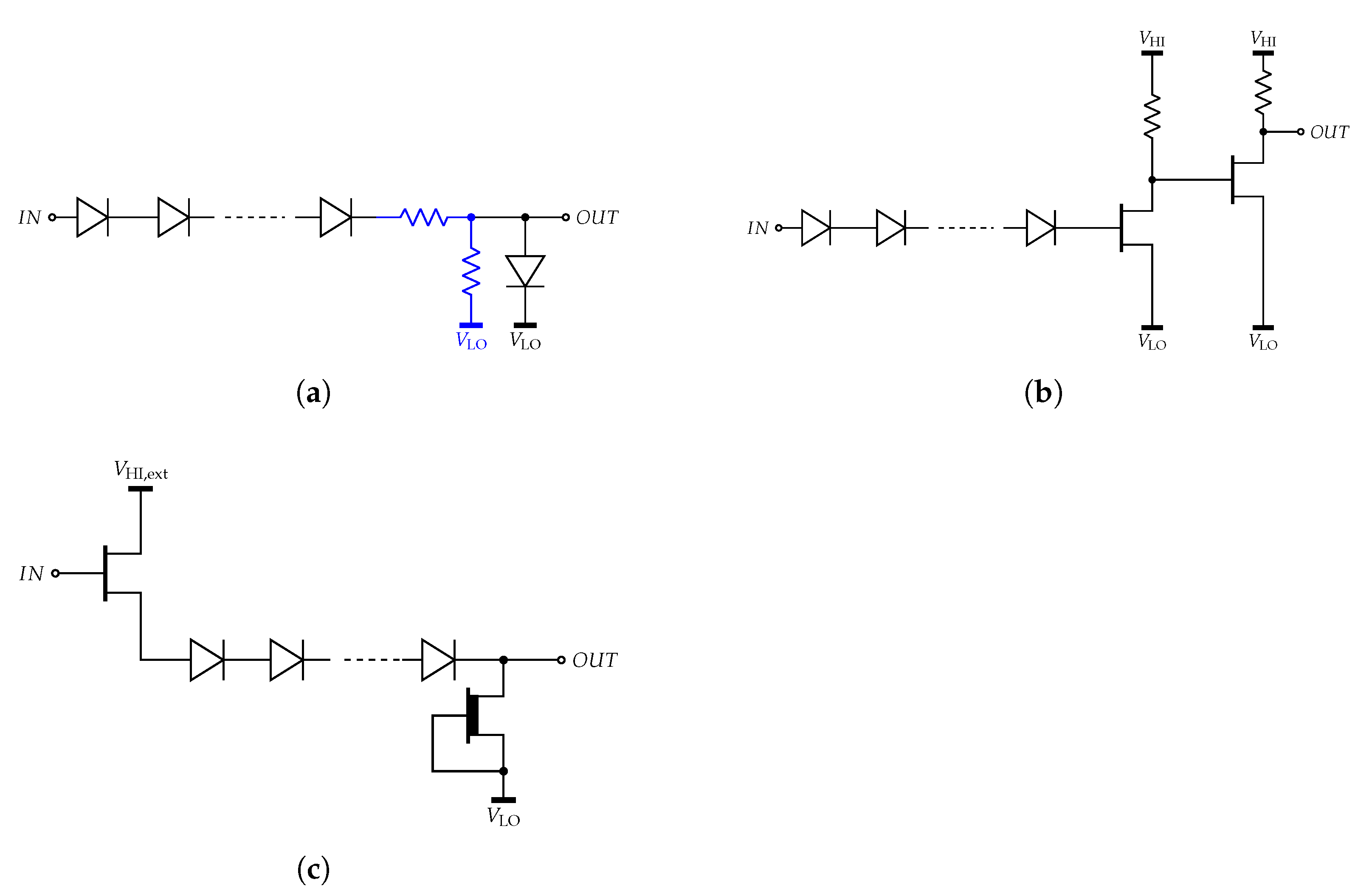
Level shifting is achieved by means of diodes, or diode-like connected transistors with drain and source terminal shunted together, in totem-pole configuration [14,15,22,31], as shown in Figure 5a. The diode/transistor type and size must be chosen accordingly to the desired voltage drop: E-mode FETs typically feature smaller saturation currents than D-mode ones and thus allow higher voltage drops, reducing the number of diodes required for level translation, but also the output voltage adjusting resolution. To overcome this limitation, a properly sized resistor can be added in series to the diodes, as shown in Figure 5a [15]. Moreover, if the voltage reference has the same value as the logic-0 input voltage, a parallel resistor maybe added to avoid leaving diodes floating as in [31]. Adopting large devices allow higher currents, resulting in a more stable voltage and a higher driving capability, eventually avoiding the need of a buffer. On the other hand, the level shifter draws the required current directly from the external input signals, thus a high demand may represent an issue in very large AESA systems, where the central unit should feed a huge number of CCs. In these cases, the adoption of a buffer stage is practically mandatory to achieve small input current leakage.
Buffer stages can be simple common source amplifiers [15]. In this case, the function of the last (output) diode of the level shifter can be accomplished by the gate-source junction of the first buffer’s transistor, as depicted in Figure 5b. Additionally, with a dedicated buffer, in order to provide high current capability, large devices may be required, which implies large capacitances and thus possible speed limitations. When high-speed operation at high current is required, the number and size of buffer stages must be carefully chosen following a tapered-buffer approach [43,44]. For example, in [15] two buffer stages have been adopted with the second stage’s transistor twice as large as that of the first stage, to ensure fast commutation and preserve input signal polarity. In [19] an interesting solution is proposed where the level shifting and the (non-inverting) buffering functions are merged together by adopting an E-mode source-follower buffer along with translating diodes and a D-mode active pull-down, as reported in Figure 5c.
Similarly, the output buffers/shifters are required to boost the current driving capability and to adjust the signals’ voltage level to what required by the analog circuitry. The latter is typically implemented with D-mode devices, hence requiring negative voltages. In [15,19,31] different examples of output buffer are presented, with or without diodes. The best topological solutions for the I/O interfaces are highly dependent on the specific input/output dynamics of the CC under development.
Hysteresis can be obtained through positive feedback by making the total loop gain higher than unity. In [45], a compact and low-power Schmitt trigger was proposed, based on two cascaded inverter stages, as shown in Figure 6 (black path). By comparing this structure with the common source buffer shown in Figure 5b it is clear that the Schmitt trigger can be easily merged with the buffer stage, by simply adding a proper feedback network. Furthermore, double inversion is the typically adopted solution to obtain two strictly symmetrical complementary signals from a single one [46,47] (black and blue outputs in Figure 6). Therefore, in differential structure, hysteresis and complementary signal generation functions can be exploited by the same circuit, while one or more further buffer stages can be added at both inputs, if necessary.
As a final remark, input signal synchronization is crucial, thus, when many input blocks are required, the best option is to replicate them for all inputs so as to ensure equal/comparable delays for all signals, even if at the price of slightly higher transistor count.
6. Memory Blocks
The simplest 1-bit memory block is the bistable circuit of Figure 7a composed of two cross-coupled NOT gates. By replacing the NOT gate with a NOR or a NAND a set/reset latch can be obtained where the bit to be stored can be fixed externally. For the NOR- and NAND-based structures to remain in the hold (memory) state with the inputs must be both 0 or both 1, respectively. To obtain a D latch an input section is added controlling how and when the set and reset commands are sent to the latch. This avoids the set and reset commands to be applied simultaneously and adds a latch enable/disable function, which can be used as level-controlled timing (clock, C) mechanism. By using, NAND or NOR gates, active-high (i.e., transparent for ) and active-low (i.e., transparent for ) D latches can be obtained, respectively. Some possible active-high configurations are shown in Figure 7. Figure 7b reports the basic differential-input D latch, while Figure 7c shows how to connect the input ports to obtain instead a single input latch with minimized gate count avoiding the additional NOT port to create from D. Note that these two architectures work also with NOR gates but becomes active-low). Finally, it is to note that in case of DCFL implementation, the pseudo-open drain (POD) effect can be exploited to simplify the circuit and reduce the transistor count, as done in [15,18]. As shown in Figure 7d, with proper sizing of the pull-up resistors, the input NANDs can be in practice considered in an open-drain state when the enable signal C is low, hence leaving unaffected the following memory block. The latter can be therefore implemented with simple NOT gates, eliminating two transistors with respect to Figure 7b. When instead the enable signal is high, the complementary outputs of the NAND ports override the memorized state, without compromising the proper operation of the cross-coupled NOTs.
Latches are sensitive to levels and thus update their outputs continuously as long as (if active-high). However, in a shift register, the data must be transferred from one bit to the following one according to the clock rate. The inputs must be thus sampled at specific instants, corresponding to either the rising or falling edge of the clock signal. The memory block that exploits this function is the D flip-flop. A D flip-flop can be built from two D latches controlled by complementary clocks: this is the common master-slave (MS) configuration, shown in Figure 8a, which is controlled by the falling clock edge (the role of C and must be exchanged to obtain a positive-edge-triggered DFF). Being connected to complementary clock signals, the two latches are never both transparent achieving the required transition-controlled behavior is achieved.
The use of differential structures, which require both true and complementary inputs, can improve noise margins, especially in case of reduced-swing signals [48]. As for the complementary clock, complementary data must be generated so as to be non-overlapping to ensure proper operation of the flip-flop. This comes at the price of larger occupied area and possibly increased power consumption, hence requiring careful optimization. The works reported in [15,18,39] exploit a differential MS (D-MS) flip-flop composed of two identical D-type latches of the kind reported in Figure 7d. Thanks to the pseudo-open drain nature of the NAND ports, the total transistor count is kept relatively low: only 12 transistors, excluding that/those for complementary clock generation and in case of E-DCFL implementation, instead of the 16 required with the classical latch structure of Figure 7b (or Figure 7c).
Master-slave DFFs can also use two different latch architectures for the two latch cells, separately optimizing each one [33]. In general, the use of MS DFFs requires a rather high number of transistors. To overcome this issue, ad hoc optimized flip-flop architectures should be evaluated/developed, such as, e.g., the modified MS flip-flop in [46], sharing one port among the two latches. In particular, for GaAs implementation, a well-established optimized structure with single input, single clock driving and minimized gates count is the 6-NOR D flip-flop [14], shown in Figure 8b. As can be noted from Table 1, this is one of the most widely adopted flip-flop architectures. It is composed of a simple set/reset latch as output stage and 2 interacting input latches, for a total of 5 two-input NORs and 1 three-input NOR. In [32], where the main target was speed, a 6-NAND structure [8] was preferred. The operating principle is totally equivalent to that of the 6-NOR one, except that it is sensitive to the opposite clock transition (negative-edge-triggered with NORs and positive-edge-triggered with NANDs). Assuming an E-DCFL implementation, the minimum number of transistor required to implement this DFF is 13. Table 3 compares the transistor count for the two analyzed DFF structures for all most relevant logic families highlighting the advantage of the 6-NOR DFF in case of buffered logics.
As anticipated in Section 3, at SIPO-level the overall transistor count can be reduced by adopting DFFs for the SR and simple latches for the HR [15,19,28]. In this way, the total number of transistor per bit is reduced to roughly 81% for the 6-NOR DFF case and down to 75% for the MS DFF case. However, latches are sensitive to levels rather than transitions, while the HR must typically respond to an edge of the external load input signal L. To adopt this solution, the load command must be given in the form of a short enable pulse rather than a transition, or better, since generating, distributing and level-shifting such a short pulse to all CCs in a phased array is practically impossible due to noise fluctuations, the external L edge must be converted into a pulse with a proper circuit on-board the CC. In [15] an example of such a circuit is reported: it is based on an analog filter (delayer) and requires only 5 active devices. The length of the enable pulse must be carefully optimized: it should be as short as possible to prevent possible instability issues, but at the same time long enough to guarantee proper data loading. In any case it must not exceed half of the clock period otherwise spurious data changes in the HR will likely happen.
7. Conclusions
With the increasing spread of electronically controlled phased arrays, the development of compact and efficient core-chips has become a crucial challenge. The embedding into such chips of a serial to parallel converter is a key benefit, allowing for increasing the number of control bits, and hence the beam-shaping accuracy, without increasing the number of external control lines. The design of low-power and low-area serial-input-parallel-output interfaces is not a trivial task in GaAs technology, due to limited metallization layers, lack of complementary devices and poor availability of digital-operation-oriented device models. In this paper, a literature review of GaAs-based serial-to-parallel converters for microwave core-chip applications has been presented, discussing the advantages and disadvantages of the different solutions, in terms of logic family and memory cell configuration.
Author Contributions
Conceptualization and visualization, C.R. and M.P.; formal analysis, investigation and data curation, C.R., M.E. and A.N.; writing—original draft preparation, C.R. and M.E.; writing—review and editing, all authors; supervision, M.P. All authors have read and agreed to the published version of the manuscript.
Funding
This research received no external funding.
Conflicts of Interest
The authors declare no conflict of interest.
References
- de Hek, A.P.; Rodenburg, M.; van Vliet, F. Low-cost S-band Multi-function MMIC. In Proceedings of the 2008 European Microwave Integrated Circuit Conference EuMIC 2008, Amsterdam, The Netherlands, 27–28 October 2008; pp. 262–265. [Google Scholar] [CrossRef]
- Ciccognani, W.; Ferrari, M.; Ghione, G.; Limiti, E.; Longhi, P.E.; Pirola, M.; Quaglia, R. A compact high performance X-band core-chip with on board serial-to-parallel conversion. In Proceedings of the 2010 40th European Microwave Conference, Paris, France, 28–30 September 2010; pp. 902–905. [Google Scholar] [CrossRef]
- Leblanc, R.; Santos Ibeas, N.; Gasmi, A.; Moron, J. Ka Band Chip-Set for Electronically Steerable Antennas. In Proceedings of the IEEE Compound Semiconductor Integrated Circuit Symposium (CSICS 2014), La Jolla, CA, USA, 19–22 October 2014; pp. 1–4. [Google Scholar] [CrossRef]
- Zhou, M.; Mo, J.; Wang, Z. A Ka-band low power consumption MMIC core chip for T/R modules. AEU-Int. J. Electron. Commun. 2018, 91, 37–43. [Google Scholar] [CrossRef]
- Giofrè, R.; Colangeli, S.; Ciccognani, W.; Costanzo, F.; Polli, G.; Salvucci, A.; Vittori, M.; Sotgia, M.; Cirillo, M.; Limiti, E. S-Band GaN Single-Chip Front End for Active Electronically Scanned Array with 40-W Output Power and 1.75-dB Noise Figure. IEEE Trans. Microw. Theory Tech. 2018, 66, 5696–5707. [Google Scholar] [CrossRef]
- Palombini, D.; Rampazzo, D.; Bentini, A.; Longhi, P.E. Design of a 5W Single Chip Front-End for C-Ku Band T/R Modules. In Proceedings of the 2018 IEEE/MTT-S International Microwave Symposium (IMS 2018), Philadelphia, PA, USA, 10–15 June 2018; pp. 647–650. [Google Scholar] [CrossRef]
- Billstrom, N.; Berg, H.; Gabrielson, K.; Hemmendorff, E.; Hertz, M. T/R “core chips” for S-, C- and, X-band radar systems. In Proceedings of the 34th European Microwave Conference (EUMC 2004), Amsterdam, The Netherlands, 12–14 October 2004; Volume 2, pp. 1029–1032. [Google Scholar]
- Ganesan, V.; Shaji, K.S. Design of positive & negative edge triggered D-flip flop using AlGaAs/GaAs MODFET technology. In Proceedings of the International Conference on Devices, Circuits and Systems (ICDCS 2014), Coimbatore, India, 6–8 March 2014; pp. 1–5. [Google Scholar] [CrossRef]
- Long, S.; Butner, S. Gallium Arsenide Digital Integrated Circuit Design; McGraw-Hill Series in Electrical Engineering: Electronics and Electronic Circuits; McGraw-Hill: New York, NY, USA, 1990. [Google Scholar]
- Sim, S.; Jeon, L.; Kim, J. A Compact X-Band Bi-Directional Phased-Array T/R Chipset in 0.13 μm CMOS Technology. IEEE Trans. Microw. Theory Tech. 2013, 61, 562–569. [Google Scholar] [CrossRef]
- Liu, C.; Li, Q.; Li, Y.; Deng, X.; Li, X.; Liu, H.; Xiong, Y. A Fully Integrated X-Band Phased-Array Transceiver in 0.13-μm SiGe BiCMOS Technology. IEEE Trans. Microw. Theory Tech. 2016, 64, 575–584. [Google Scholar] [CrossRef]
- Nguyen, V.V.; Nam, H.; Choe, Y.; Lee, B.H.; Park, J.D. An X-band Bi-Directional Transmit/Receive Module for a Phased Array System in 65-nm CMOS. Sensors 2018, 18, 2569. [Google Scholar] [CrossRef] [Green Version]
- Van Tuyl, R.; Liechti, C.; Lee, R.; Gowen, E. GaAs MESFET logic with 4-GHz clock rate. IEEE J. Solid-State Circuits 1977, 12, 485–496. [Google Scholar] [CrossRef]
- Wing, O. Gallium Arsenide Digital Circuits; Kluwer Academic Publosher: Boston, MA, USA, 1990. [Google Scholar]
- Ramella, C.; Longhi, P.E.; Pace, L.; Nasri, A.; Ciccognani, W.; Pirola, M.; Limiti, E. Ultralow-Power Digital Control and Signal Conditioning in GaAs MMIC Core Chip for X-Band AESA Systems. IEEE Trans. Microw. Theory Tech. 2021. [Google Scholar] [CrossRef]
- Komiak, J.; Agrawal, A. Design and performance of octave S/C band MMIC T/R modules for multi-function phased arrays. IEEE Trans. Microw. Theory Tech. 1991, 39, 1955–1963. [Google Scholar] [CrossRef]
- de Boer, A.; Mouthaan, K. GaAs Mixed Signal Multi-Function X-Band MMIC with 7 Bit Phase and Amplitude Control and Integrated Serial to Parallel Converter. In Proceedings of the 2000 30th European Microwave Conference, Paris, France, 2–5 October 2000; pp. 1–4. [Google Scholar] [CrossRef] [Green Version]
- Zhou, S.; Zhou, S.; Zhang, J.; Wu, J.; Yang, H.; Wang, Z. A 7.5–9 GHz GaAs Two-Channel Multi-Function Chip. Electronics 2019, 8, 395. [Google Scholar] [CrossRef] [Green Version]
- Lee, H.; Kim, Y.; Lee, I.; Kim, D.; Park, K.; Jeon, S. A Ku-Band GaAs Multifunction Transmitter and Receiver Chipset. Electronics 2020, 9, 1327. [Google Scholar] [CrossRef]
- Jeong, J.C.; Kwak, C.; Yom, I.B.; Seo, I.J.; Jo, I.H. Life test of an X-band MMIC multi-function chip for active phased array radar applications. Microel. Reliab. 2015, 55, 815–821. [Google Scholar] [CrossRef]
- Willms, J.G.; Ouacha, A.; de Boer, L.; van Vliet, F.E. A Wideband GAAS 6-Bit True-Time Delay MMIC Employing On-Chip Digital Drivers. In Proceedings of the European Microwave Conference (EuMW 2000), Paris, France, 2–5 October 2000; pp. 1–4. [Google Scholar] [CrossRef]
- Bentini, A.; Pasciuto, B.; Ciccognani, W.; Limiti, E.; Nanni, A.; Romanini, P. Design and Realization of GaAs Digital Circuit forMixed Signal MMIC Implementation in AESA Applications. Int. J. Microw. Sci. Technol. 2011. [Google Scholar] [CrossRef] [Green Version]
- Robert, F.; Leblanc, R.; Moron, J.; Gasmi, A.; Santos, N.; Rocchi, M. E/D GaAs PHEMT Core Chips for Electronically Steerable Antennas. Microw. J. 2012, 55, 98–106. [Google Scholar]
- Jeong, J.C. An S-Band Multifunction Chip with a Simple Interface for Active Phased Array Base Station Antennas. ETRI J. 2013, 35, 378–385. [Google Scholar] [CrossRef]
- Pirola, M.; Quaglia, R.; Ghione, G.; Ciccognani, W.; Limiti, E. 13-bit GaAs serial-to-parallel converter with compact layout for core-chip applications. Microelectron. J. 2014, 45, 864–869. [Google Scholar] [CrossRef]
- Shin, D.H.; Jeong, J.C.; Moon, S.M.; Yom, I.B.; Kim, D.W. Compact Ku-band GaAs multifunction chip for SATCOM phased arrays. In Proceedings of the European Microwave Conference (EuMC), Paris, France, 7–10 September 2015; pp. 449–452. [Google Scholar] [CrossRef]
- Jiang, Y.; Jiang, X.; Li, Y.; Hong, W. Design and realization of a 13-bit serial to parallel GaAs digital circuit for 6–18 GHz T/R module. In Proceedings of the IEEE International Conference Ubiquitous Wireless Broadband (ICUWB 2016), Nanjing, China, 16–19 October 2016; pp. 1–3. [Google Scholar] [CrossRef]
- Harris, M.; Gui, P. A 12-bit serial-to-parallel converter using depletion-mode-only devices. In Proceedings of the Texas Symposium on Wireless and Microwave Circuits and Systems (WMCS 2017), Waco, TX, USA, 30–31 March 2017; pp. 1–4. [Google Scholar] [CrossRef]
- Jeong, J.C.; Yom, I.B.; Kim, J.D.; Lee, W.Y.; Lee, C.H. A 6–18-GHz GaAs Multifunction Chip With 8-bit True Time Delay and 7-bit Amplitude Control. IEEE Trans. Microw. Theory Tech. 2018, 66, 2220–2230. [Google Scholar] [CrossRef]
- Jeong, J.; Uhm, M.; Jang, D.; Yom, I. A Ka-band GaAs Multi-function Chip with Wide-band 6-bit Phase Shifters and Attenuators for Satellite Applications. In Proceedings of the 2019 13th European Conference on Antennas and Propagation (EuCAP), Krakow, Poland, 31 March–5 April 2019; pp. 1–4. [Google Scholar]
- Kim, D.S.; Yeom, K.W. Compact 4-bit GaAs Ku-band core chips for phased arrays. Microw. Opt. Technol. Lett. 2020, 62, 2289–2299. [Google Scholar] [CrossRef]
- Stesev, G.; Budanov, D.; Balashov, E. Serial-to-Parallel Converter Using GaAs D-Mode Transistors. In Proceedings of the 2020 IEEE International Conference on Electrical Engineering and Photonics, St. Petersburg, Russia, 15–16 October 2020; pp. 67–70. [Google Scholar] [CrossRef]
- Kanopoulos, N. Gallium Arsenide Digital Integrated Circuits: A Systems Perspective; Prentice Hall: Hoboken, NJ, USA, 1989. [Google Scholar]
- JEDEC. POD1X-1.X V Pseudo Open Drain I/O. Available online: https://www.jedec.org (accessed on 9 November 2021).
- Kalia, K.; Pandey, B.; Nanda, K.; Malhotra, S.; Kaur, A.; Hussain, D.M.A. Pseudo open drain IO standards based energy efficient solar charge sensor design on 20 nm FPGA. In Proceedings of the IEEE 11th International Conference on Power Electronics and Drive Systems (ICPEDS 2015), Sydney, Australia, 9–12 June 2015; pp. 367–372. [Google Scholar] [CrossRef]
- Deming, R.; Zucca, R.; Vahrenkamp, R.; Hou, L.; Naused, B.; Gilbert, B. A gallium arsenide configurable cell array using buffered FET logic. IEEE J. Solid-State Circuits 1984, 19, 728–738. [Google Scholar] [CrossRef]
- Nakamura, H.; Tanaka, K.; Tsunotani, M.; Kawakami, Y.; Akiyama, M.; Kaminishi, K. A 390ps 1000-gate array using GaAs super-buffer FET logic. In Proceedings of the IEEE International Solid-State Circuits Conference. Digest of Technical Papers, New York, NY, USA, 13–15 February 1985; Volume XXVIII, pp. 204–205. [Google Scholar] [CrossRef]
- Ghione, G.; Pirola, M.; Quaglia, R.; Ciccognani, W.; Limiti, E.; Cavanna, T. Compact GaAs HEMT D flip-flop for the integration of a SAR MMIC core-chip digital control logic. In Proceedings of the 2010 International Workshop Integrated Nonlinear Microwave and Millimetre-Wave Circuits (INMMiC), Gothenburg, Sweden, 26–27 April 2010; pp. 62–65. [Google Scholar] [CrossRef]
- Ramella, C.; Longhi, P.E.; Nasri, A.; Pace, L.; Ciccognani, W.; Estebsari, M.; Pirola, M.; Limiti, E. Low Power GaAs Digital and Analog Functionalities for Microwave Signal Conditioning in AESA Systems. In Proceedings of the International Workshop Integrated Nonlinear Microwave Millimetre-Wave Circuits (INMMiC 2020), Cardiff, UK, 16–17 July 2020; pp. 1–3. [Google Scholar] [CrossRef]
- Statz, H.; Newman, P.; Smith, I.; Pucel, R.; Haus, H. GaAs FET device and circuit simulation in SPICE. IEEE Trans. Electron Devices 1987, 34, 160–169. [Google Scholar] [CrossRef]
- Hallgren, R.; Litzenberg, P. TOM3 capacitance model: Linking large- and small-signal MESFET models in SPICE. IEEE Trans. Microw. Theory Tech. 1999, 47, 556–561. [Google Scholar] [CrossRef]
- Angelov, I.; Bengtsson, L.; Garcia, M. Extensions of the Chalmers nonlinear HEMT and MESFET model. IEEE Trans. Microw. Theory Tech. 1996, 44, 1664–1674. [Google Scholar] [CrossRef]
- Li, N.; Haviland, G.; Tuszynski, A. CMOS tapered buffer. IEEE J. Solid-State Circuits 1990, 25, 1005–1008. [Google Scholar] [CrossRef]
- Tinivella, R.; Camarchia, V.; Pirola, M.; Shen, S.; Ghione, G. Simulation and design of OFET RFIDs through an analog/digital physics-based library. Org. Electron. 2011, 12, 1328–1335. [Google Scholar] [CrossRef]
- Al-Sarawi, S. Low power Schmitt trigger circuit. Electron. Lett. 2002, 38, 1009–1010. [Google Scholar] [CrossRef]
- Shizuku, Y.; Hirose, T.; Kuroki, N.; Numa, M.; Okada, M. A 24-transistor static flip-flop consisting of nors and inverters for low-power digital vlsis. In Proceedings of the IEEE 12th International New Circuits and Systems Conference (NEWCAS 2014), Trois-Rivieres, QC, Canada, 22–25 June 2014; pp. 137–140. [Google Scholar] [CrossRef]
- Tsai, M.Y.; Kuo, P.Y.; Lin, J.F.; Sheu, M.H. An Ultra-low-power True Single-phase Clocking Flip-flop with Improved Hold time Variation using Logic Structure Reduction Scheme. In Proceedings of the International Symposium on Circuits and Systems (ISCAS 2018), Florence, Italy, 27–30 May 2018; pp. 1–4. [Google Scholar] [CrossRef]
- Weste, N.; Harris, D. CMOS VLSI Design: A Circuits and Systems Perspective; Pearson Education: London, UK, 2011. [Google Scholar]
Figure 1.
Basic block diagram of a microwave core-chip. The SIPO interface (red) controls the RF analog part which includes a phase shifter (PS), an attenuator (ATT) and some switches (SW). All amplifiers are optional and the TX input/RX output can either have separate pads (blue) or share the same pad, hence the number of switches depends on the specific CC architecture considered.

Figure 2.
n-bit SIPO interface.

Figure 3.
Inverter gate () implementations in different FET logic families. (a) D-mode buffered FET logic: (left) origial scheme (D-BFL) and (right) HVR-shifter version (HVR-BFL). (b) Direct-coupled FET logic: (left) E-mode scheme (E-DCFL) and (right) E/D mode scheme. (c) Buffered E/D-mode logic: (left) output source-follower buffered (BDCFL/EDSF) and (right) super-buffered (SBFL/EDSB).

Figure 4.
Examples of NAND and NOR gates in different FET logic families: (left) HVR-BFL 2-input NAND, (center) E-DCFL 2-input NOR, (right) SBFL 2-input NOR.
Figure 4.
Examples of NAND and NOR gates in different FET logic families: (left) HVR-BFL 2-input NAND, (center) E-DCFL 2-input NOR, (right) SBFL 2-input NOR.

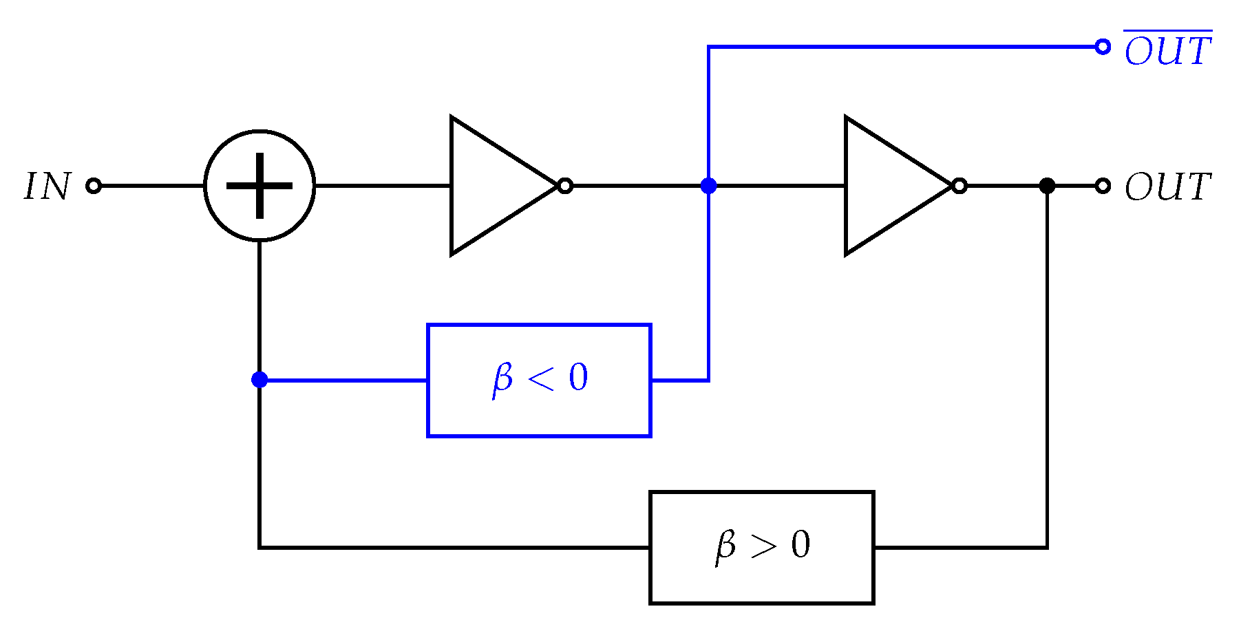
Figure 5.
Input level shifters: (a) Basic level shifter with optional (blue) series/shunt resistors, adopted for example in [15,22,31]. (b) Level shifter with common source buffer, adopted for example in [15]. (c) Level shifter with source follower buffer, adopted for example in [19]. Note that in all schemes diodes can be replaced by diode-connected transistors.

Figure 6.
Schmitt trigger implemented with a double inverter. The complementary output is optionally available and/or can be optionally used to create the positive feedback (blue paths).
Figure 6.
Schmitt trigger implemented with a double inverter. The complementary output is optionally available and/or can be optionally used to create the positive feedback (blue paths).

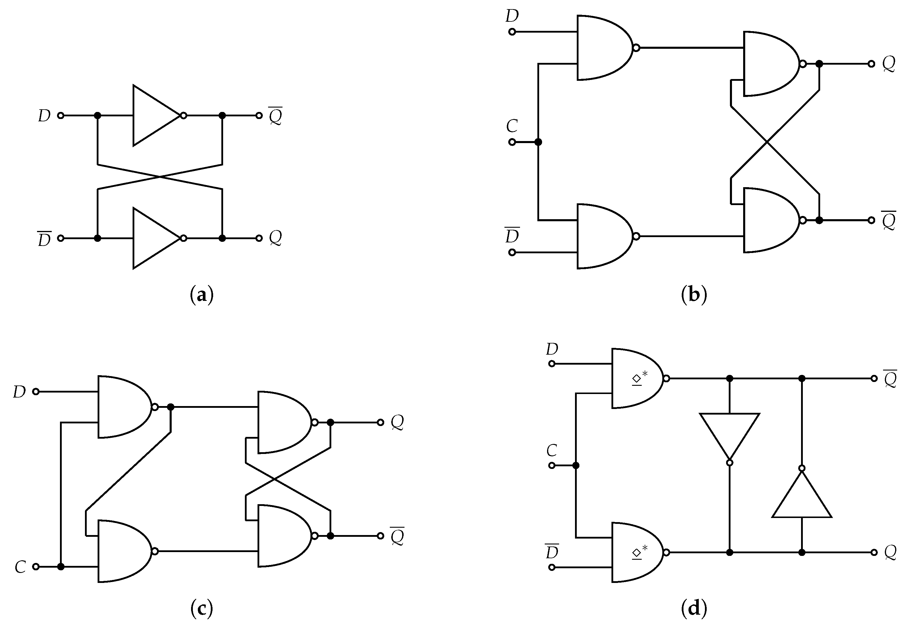
Figure 7.
Basic level-controlled memory blocks (latches). (a) Cross-coupled inverters. (b) 4-NAND differential-input active-high D latch. (c) 4-NAND single-input active-high D latch. (d) Simplified differential-input active-high D latch with pseudo-open collector NANDs.
Figure 7.
Basic level-controlled memory blocks (latches). (a) Cross-coupled inverters. (b) 4-NAND differential-input active-high D latch. (c) 4-NAND single-input active-high D latch. (d) Simplified differential-input active-high D latch with pseudo-open collector NANDs.

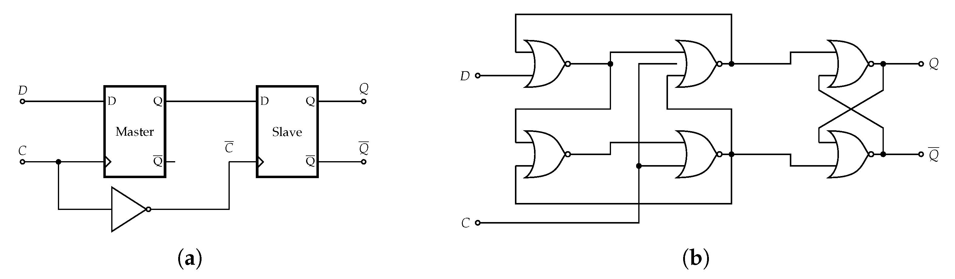
Figure 8.
D-type flip-flops. (a) Master-slave DFF. (b) 6-NOR DFF.


Table 1.
State of the art of GaAs-based SIPO interfaces for CC applications.
| Ref. | Technol. | Logic Family | DFF Architecture | Transistors/DFF | Num. bits (PS + AT + SW) | Consumption (mW/bit) | CLK Speed (MHz) |
|---|---|---|---|---|---|---|---|
| [16] | N.A. (E/D) | BFL | N.A. | N.A. | 12 (8 + 8 + 0) | N.A. | 25 |
| [17] | 0.18 m E/D | DCFL | N.A. | N.A. | 16 (7 + 7 + 2) | 4.4 | 0.1–20 |
| [21] | 0.18 m E/D | DCFL | N.A. | N.A. | 6 (6 + 0 + 0) | 5 | 20 |
| [22] | 0.4 m E/D | SBFL | 6-NOR | 38 | 8 (N.A.) | N.A. | N.A. |
| [23] | 0.18 m E/D | E-DCFL | N.A. | N.A. (46/bit) | 26 (12 + 12 + 2) | 2.3 | N.A. |
| [24] | 0.5 m E/D | DCFL | N.A. | N.A. | 12 (6 + 6 + 0) | 11 | N.A. |
| [25] | 0.18 m E/D | SBFL | 6-NOR | 38 | 13 (6 + 6 + 1) | 17 | 40 |
| [26] | 0.5 m E/D | DCFL | N.A. | N.A. | 8 (4 + 4 + 0) | 17 | N.A. |
| [20] | 0.5 m E/D | DCFL | N.A. | N.A. | 24 (6 + 6 + 1) | 11 | N.A. |
| [27] | 0.15 m E/D | DCFL | 6-NOR | 19 | 13 (6 + 6 + 1) | N.A. | N.A. |
| [28] | 0.5 m D | HVR-BFL | N.A. | N.A. | 12 (N.A.) | 63.8 | 100 |
| [29] | 0.25 m E/D | DCFL | 6-NOR | N.A. | 15 (8 + 7 + 0) | 6.8 | 24 |
| [18] | 0.5 m E/D | DCFL | D-MS | 20 | 27 (12 + 12 + 2) | 2.6 | 10 |
| [30] | 0.5 m E/D | DCFL | N.A. | N.A. | 12 (6 + 6 + 0) | 6.6 | N.A. |
| [31] | 0.25 m E/D | E-DCFL | 6-NOR | 13 | 4 (4 + 0 + 0) | 10.6 | N.A. |
| [32] | 0.5 m D | HVR-BFL | 6-NAND | 31 | 4 (N.A.) | 700 * | 3000 * |
| [19] | 0.25 m E/D | DCFL | 6-NOR | N.A. | 9 (4 + 5 + 0) | 39–46 | N.A. |
| [15] | 0.25 m E/D | E-DCFL | D-MS | 12 | 18 (6 + 6 + 6) | 2.2 | 50 |
* Simulation only.
Table 2.
GaAs FET logic gate families.
| FET Type | Logic Family |
|---|---|
| D-mode | Unbuffered FET logic (UFL/FL) |
| Buffered FET logic (BFL) | |
| Schoktty diode FET logic (SDFL) | |
| Buffered diode FET logic (BDFL) | |
| Capacitor-diode FET logic (CDFL) | |
| Capacitive-coupled FET logic (CCFL) | |
| Pass transistor/Transmission gate logic | |
| E-mode | Quasi-FET logic (QFL) |
| Direct coupled FET logic (DCFL) | |
| Buffered direct coupled FET logic (BDCFL) | |
| Source-coupled FET logic (SCFL) | |
| Feedback FET Logic (FFL) | |
| Pseudo-Complementary FET Logic (PCFL) | |
| E/D-mode | Direct coupled FET logic (DCFL) |
| Buffered E/D FET logic (BFL/EDB/EDSF/SDCFL/SFED) | |
| Buffered E/D FET logic with diode (EDSFD) | |
| Super-buffered E/D FET logic (SBFL/EDSB) | |
| Source-coupled FET logic (SCFL) | |
| FET-FET logic (F2L) |
Table 3.
D flip-flop transistor count for the different logic families of Figure 3: comparison between the MS DFF and the 6-NOR/6-NAND DFF.
Table 3.
D flip-flop transistor count for the different logic families of Figure 3: comparison between the MS DFF and the 6-NOR/6-NAND DFF.
| Logic Family | MS DFF * | 6-NOR DFF |
|---|---|---|
| E-DCFL | 16 (or 12 †) | 13 |
| DCFL | 24 (or 20 †) | 19 |
| BFL | 40 | 31 |
| SBFL | 48 | 38 |
* 2 × 4-NAND latch version; excluding transistor(s) for complementary clock generation. † By exploiting the POD feature of the DCFL (2-NAND + 2-NOT latches).
Publisher’s Note: MDPI stays neutral with regard to jurisdictional claims in published maps and institutional affiliations. |
© 2021 by the authors. Licensee MDPI, Basel, Switzerland. This article is an open access article distributed under the terms and conditions of the Creative Commons Attribution (CC BY) license (https://creativecommons.org/licenses/by/4.0/).
Share and Cite
MDPI and ACS Style
Ramella, C.; Estebsari, M.; Nasri, A.; Pirola, M. GaAs-Based Serial-Input-Parallel-Output Interfaces for Microwave Core-Chips. Electronics 2021, 10, 3029. https://0-doi-org.brum.beds.ac.uk/10.3390/electronics10233029
AMA Style
Ramella C, Estebsari M, Nasri A, Pirola M. GaAs-Based Serial-Input-Parallel-Output Interfaces for Microwave Core-Chips. Electronics. 2021; 10(23):3029. https://0-doi-org.brum.beds.ac.uk/10.3390/electronics10233029
Chicago/Turabian StyleRamella, Chiara, Motahhareh Estebsari, Abbas Nasri, and Marco Pirola. 2021. "GaAs-Based Serial-Input-Parallel-Output Interfaces for Microwave Core-Chips" Electronics 10, no. 23: 3029. https://0-doi-org.brum.beds.ac.uk/10.3390/electronics10233029
Note that from the first issue of 2016, this journal uses article numbers instead of page numbers. See further details here.