
Unbalanced-Tests to the Improvement of Yield and Quality


Department of Electrical Engineering, National Central University, Taoyuan 320317, Taiwan
*
Author to whom correspondence should be addressed.
†
Two authors contribute equally to this work.
Electronics 2021, 10(23), 3032; https://0-doi-org.brum.beds.ac.uk/10.3390/electronics10233032
Submission received: 27 October 2021
/
Revised: 28 November 2021
/
Accepted: 2 December 2021
/
Published: 4 December 2021
(This article belongs to the Section Circuit and Signal Processing)
Abstract
:An integrated-circuit testing model (DITM) is used to describe various factors that affect test yield during a test process. We used a probability distribution model to evaluate test yield and quality and introduced a threshold test and a guardband test. As a result of the development speed of the semiconductor manufacturing industry in the future being unpredictable, we use electrical properties of existing products and the current manufacturing technology to estimate future product-distribution trends. In the development of very-large-scale integration (VLSI) testing, the progress of testing technology is very slow. To improve product testing yield and quality, we change the test method and propose an unbalanced-test method, leading to improvements in test results. The calculation using our proposed model and data estimated by the product published by the IEEE International Roadmap for Devices and Systems (IRDS, 2017) proves that the proposed unbalanced-test method can greatly improve test yield and quality and achieve the goal of high-quality, near-zero-defect products.
1. Introduction
Due to the rapid development of semiconductor process capabilities, the progress rate of the future process has become unpredictable. Thus, estimating future product distribution trends using current manufacturing capability and existing product electrical characteristic parameters and conditions is a critical topic. In this study, we used a digital integrated-circuit (DITM) test model [1,2,3,4] using the existing manufacturing technology along with the electrical performance of existing products to estimate the future distribution trend of IC products. According to an update to the International Technology Roadmap for Semiconductors (ITRS), manufacturing speed and testing progress will significantly change in the future, with product manufacturability increasing by 30% annually and testing abilities rising by 12% annually [5,6,7]. This indicates that testing capabilities have not kept up with the capabilities of the semiconductor manufacturing technology. Hence, if the test method for future semiconductor products remains unchanged, test yield will reduce due to tester inaccuracy [8,9], thereby posing a serious challenge for companies performing tests.
In the highly competitive semiconductor industry, effective cost control is always the key to success, and manufacturing technology advancement and length of testing time are the main factors that determine the cost. For semiconductor manufacturing, promoting capacity, improving manufacturing methods, lowering product defect rate, shortening manufacturing time are the methods to reduce production cost. However, due to the influence of the global pandemic (COVID-19), the production of chips has been significantly reduced. The entire supply chain of the semiconductor industry has been affected. Conversely, the pandemic (COVID-19) has caused a significant increase in the demand for chips, resulting in shortages in the mobile phone, automobile, and notebook industries. Considering the current material scarcity in the global semiconductor industry, growing the usable capacity has become urgent in order to increase usable chips under limited production capacity. The capacity of testing houses has decreased (COVID-19) due to the global recession of the semiconductor industry, causing many testers to remain idle in the testing factories. If an effective testing method for making the best use of idle testers to promote test yield and quality could be adopted, then cost could be saved, and the quality of semiconductor components could be controlled strictly. Thus, products with high quality could be used to promote product profit.
In the automotive industry, the importance of the quality control of automotive electronic products and automotive electronic parts often overrides the functionality of the parts. Furthermore, the modes of consumption and concept (mentality) of consumers have changed, increasing demand for high-quality products (Biomedical Electronics and Automotive Electronics). Therefore, IC suppliers have invested heavily in production and test equipment and have proposed many methods to ensure that the quality goal of zero defects is achieved. To address the issues above, we proposed an unbalanced test method that involves moving the test guardband (TGB) to retest the chips that failed the previous test, thereby reducing the killing errors and missing errors chips and increasing the product reliability (Biomedical Electronics and Automotive Electronics). We have repeatedly searched for reliable products because we used the idle IC tester to improve the yield after testing and the move testing guardband method. The problem of chip shortages can be partially solved as the number of available chips has increased.
2. Calculating Manufacturing Yield (Ym) and Predicting Manufacturing Progress Variation
Very-large-scale integration (VLSI) chips were developed through the stages of conceptualization, manufacturing, and finishing to obtain a final product (Figure 1). During a VLSI chip development process, a number of chips (N) are manufactured, once they are fabricated, they are separated into two parts: bad (B) and good (G). True yield or manufacturing yield Ym can be expressed as Ym = G/N. Owing to uncertain factors in a semiconductor manufacturing environment, the electrical characteristics of a product are shifted during a manufacturing process; therefore, the electrical properties of each produced chip are different. In this paper, we assume the chip delay time of device under test (DUT) is normal.
Due to uncertainty factors in the manufacturing environment (mask error, etching and chemical concentration errors) after manufacturing, we assume the chip delay time of a device under test (DUT) is normal. Therefore, chip(x) = N(x; μM, σM) with mean μM and standard deviation σM [2,3,4]:
(Ym) is the probability of the area under the normal curve between the coordinates x = − and x = DS, i.e., P [ < X < DS]. Thus, Ym
where DS is the design specification.
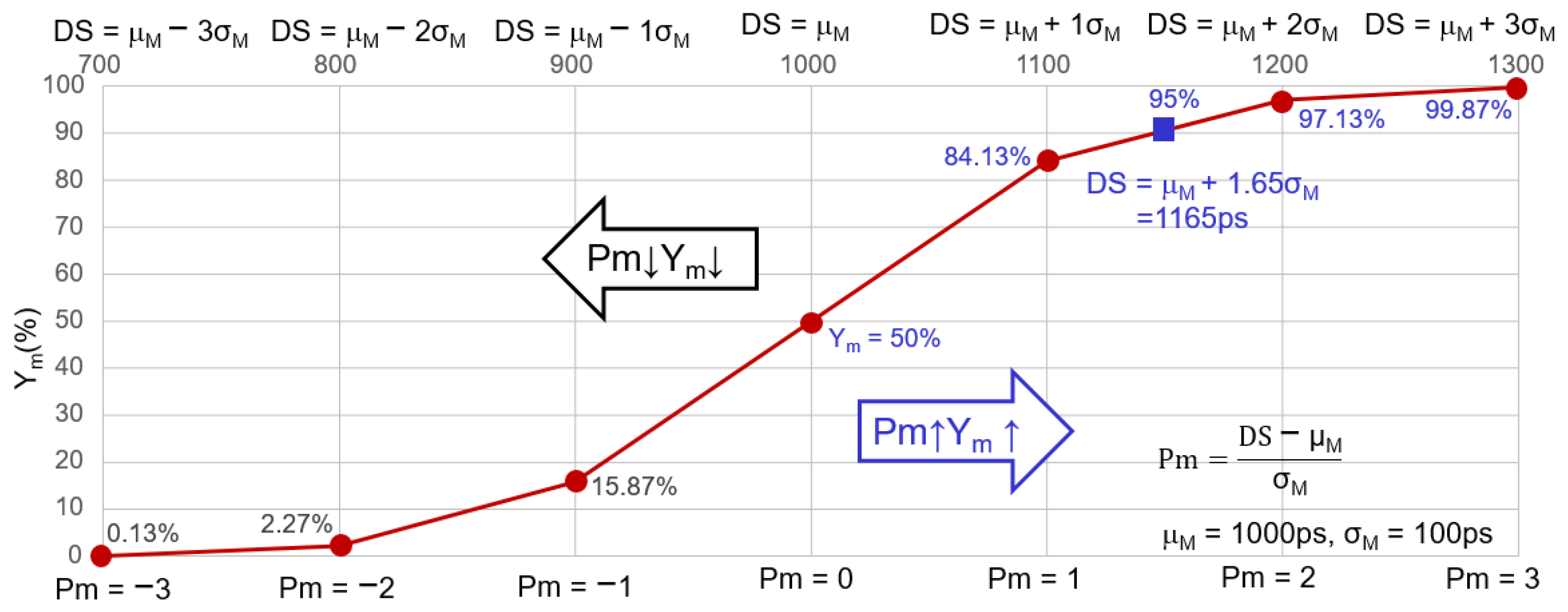
For example, for chips with a design specification (DS) 1165 ps and circuit characteristic parameter X~N (x; μM = 1000 ps and σM = 100 ps), standard deviation σM is 100 ps and the average of normal distribution μM is 1000 ps. Assuming DS is 0.858 GHz (DS = 1165 ps), products that meet the DS can be classified as “good,” and those that do not meet the DS can be classified as “bad.” According to the abovementioned data, we can obtain 95% manufacturing yield (true yield), Ym = P [Good] = P [X < DS] = 95%, where P [ < X < DS] indicates that the random parameter x lies between the probability of x = and x = DS, or
Distribution Trend of Manufacturing Progress and Product Variation
In a real manufacturing environment, there inevitably exists uncertain factors such as temperature and exposure errors, chemical concentration errors during etching, and the shifting of the electrical properties of components. The performance of every produced chip is therefore different. These manufacturing parameters inevitably affect the manufacturing yield. The parameters include product manufacturability (Pm), which is expressed as
A higher Pm value means a better manufacturing ability than the design ability and a higher manufacturing yield. As shown in Figure 2, in this situation, given DS = 1100 ps (DS = μM + 1 σM = 1100 ps), DUT characteristics X~N (x; 1000 ps and 100 ps), then Pm = 1 and Ym = 84.13%. In addition, a tested device can have X~N (x; μM = 1000 ps, σM = 100 ps) characteristics, wherein the DS is equal to 900 ps. As per the above procedure, we obtain the manufacturing yield as 15.87% and Pm as −1. When the Pm was gradually lowered, the manufacturing variation increased, and its linear variation was more significant; thus, the larger the manufacturing variation, the lower the manufacturing yield (Ym).
Semiconductors are rapidly advancing, and process technology is rapidly changing. Developing the best method to apply the current process technology and product characteristics to estimate future product forecast curves is crucial for manufactures. With the rapid progress of the semiconductor manufacturing process, the complexity of the chips has been increasing, and the size of the components has been decreasing at an exponential rate. When the cross-sectional area is reduced by half, the variation value of the electrical characteristic parameters of the chip and the mismatch relationship increases. Many process changes that are difficult to control also occur. Therefore, we define a process progress parameter to indicate the degree of process progress. Even a slight change in the process progress parameter may greatly affect the product manufacturing yield. Here, assuming the DUT distribution is normally distributed, we use appropriate manufacturing schedule parameters (α) and current manufacturing technology to estimate parameters of future product attributes. We adopt the following calculation formula:
For example, we applied Equations (5) and (6) to the chip data from the International Roadmap for Devices and Systems 2017 [10], using DS = 400 ps (2.5 GHz), with circuit-property parameter N (x; μM = 264 ps, σM = 83 ps) for the year 2018 (Table 1), assuming Ym = 95% when Pm = 1.65, and setting α = 1 (manufacturing progress parameter). Then, and were substituted into Equations (5) and (6), and the 2019 circuit-property parameter was estimated as X~N (x; μM = 233 ps, σM = 73 ps).
3. Calculating the Testing Yield (Yt) and Defect Level (DL)
A threshold test was applied to the digital circuit performance parameter test (Figure 1). For the time parameter X of the tested circuit, the tester sends a strobe (ST), and then the comparator will make a judgment (pass and fail). Because of the problem of the tester accuracy, the ST sent by the tester will have an edge placement; that is, the actual ST will be a bit faster or slower than the set time. Therefore, the signal sent by the tester presents a probability distribution value instead of a single fixed value.
3.1. Evaluation of Test Yield (Threshold Test)
This thesis assumes that the test capability (tester) is normally distributed, X~N (x; μT, σT); the average μT equals the test specification (TS), and μT = TS; therefore, the decision of TS is related to the test yield and test quality. Moreover, Yt is calculated as Yt = P[pass] = P[X < Y] and expressed as
Let denote that the traditional test method is used to test the device, and the test is conducted only once.
3.2. Test Specifications (Test Guardband) Impact on Test Yield and Defect Level
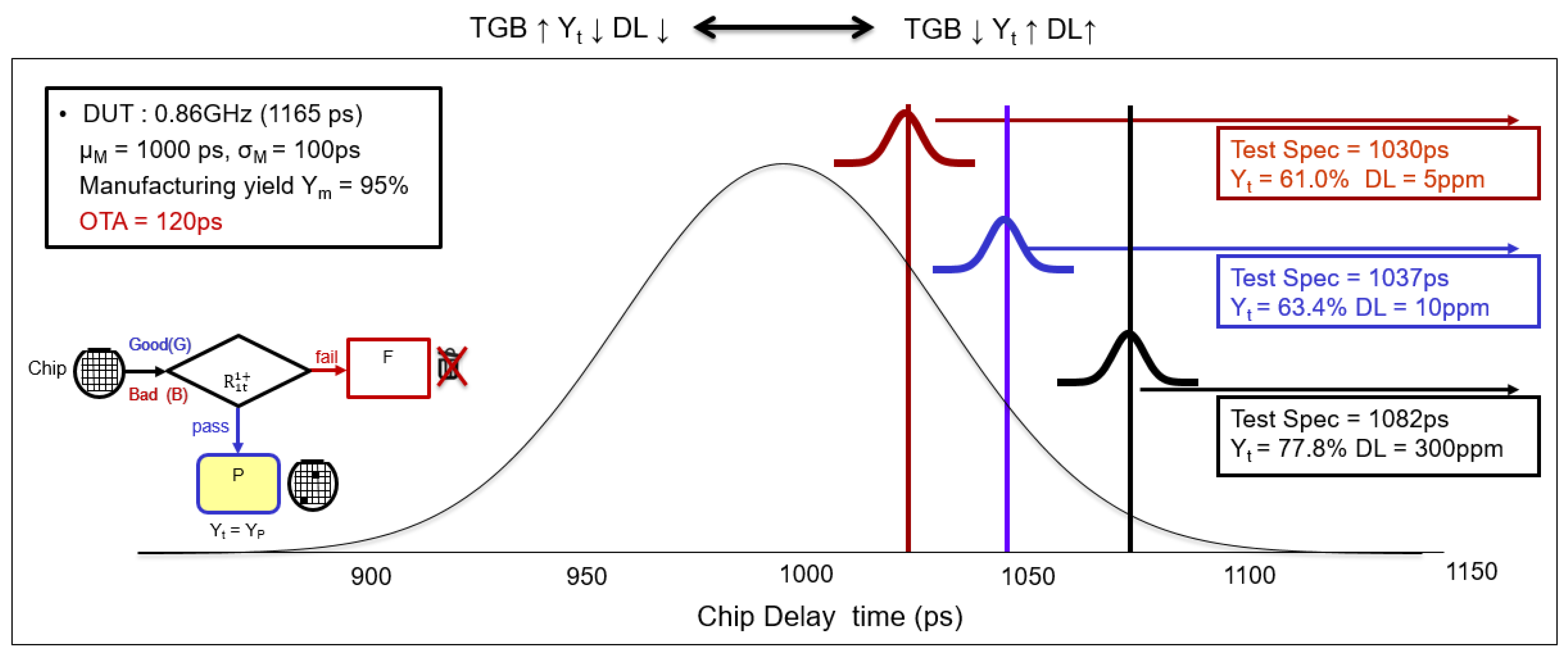
Testing error inevitably exists. Besides testing the yield, the most important thing is testing the quality. The defect level (DL) denotes the ratio of the defective parts over the shipped chips, and it is usually used as a product quality measure, evaluated as parts per million (ppm). Taking the Intel CPU used in desktop computers as an example, the DL acceptable to consumers is 200–300 ppm. Some key electronic products have high-reliability requirements, with DL = 10 ppm. Therefore, to ensure the reliability of key electronic products, strict quality control is needed. Generally, test protection is used to eliminate all defective parts in the total parts, but it will cause a loss in the test yield.
If the testing process is not perfect, possibly because of some errors, problems of tester accuracy, or problems regarding TS/guardband test. For instance, when DS = 1165 ps, DUT is N (x; 1000 ps and 100 ps), and Ym is 95%, the mean test capability is set to TS = μT, and the test standard deviation (σT) is set to one-third of the overall time accuracy (OTA). Thus, if OTA = 3 × σT = 120 ps, then σT = 40 ps. As per the above procedure, if μT = 1082 ps, the required DL = P[Bad|Pass] = P[(X > DS)∩(X < ST)]/P[X < ST] = 300 ppm, and yield loss is 17.2% (95% − 77.8%) (Figure 3). Following the described procedure, when the test was conducted once, and the TS was set to 1030 ps, the obtained test yield (Yt) was 61.0% while the desired DL (5 ppm) was maintained, and the yield loss was 34% (95% − 61.0%). Thus, a lower Yt and DL were obtained with stricter TS. Considering the problem of tester inaccuracy, a test guardband (TGB) should be used [11,12]. The test guardband is defined as the distance between DS and TS. Since manufacturing defects can cause product defects, the test guardband must be appropriately adjusted to remove most defective products during the testing process. When traditional testing methods are used, the wider the test guardband range, the higher the promised quality of delivered goods, although the killing-error rate will be higher, and fewer products can pass the tester. On the contrary, the smaller the test guardband range, the higher the yield of the delivered goods, but the product quality will decrease. Therefore, the test guardband must be appropriately moved to obtain the best test results and meet customer needs.
4. New Unbalanced Testing Scheme
As a result of the COVID-19 pandemic, most people have been confined at home for a long time, and the large-scale use of 3C products has caused the demand for consumer electronics chips to surge. Simultaneously, automakers are forced to reduce chips due to the rapid decline in sales in the automotive industry. Afterward, the spread of COVID-19 gradually slowed down, and the automotive market had made an unexpected rebound. Thus, as the consumer electronics industry snatched up global chips, automotive chip manufacturers faced a serious shortage of materials. Due to the current interference from the pandemic and lack of labor and materials, the output of the chips produced by semiconductor factories still cannot meet the demand of consumers. However, we have found that the overall development speeds of testing and of manufacturing technologies are different [5,6,7], whereby the improvement of testing technology is lagging behind the improvement of design and manufacturing technologies. The slow improvements in testing equipment and processes can make the future of this technology unclear. Therefore, semiconductor manufacturers have begun to invest huge amounts of money to improve process equipment and have proposed many effective testing and verification methods to reduce the entry of defective products into the market.
Currently, in the very-large-scale integration testing industry, retesting is being applied in the production process to improve test results [13,14,15]. For example, TT (Teslence Technology Co., Ltd., Taipei City, Taiwan) assists the test plant ASE Technology Holding Co., Ltd. (Kaoshiung, Taiwan) to develop new test methods [16], using smart methods of retesting chips and applying them to the actual test production line. After the actual test and record have been applied for a period, the retest method can effectively improve the test yield. Additionally, for at-speed testing, the on-chip clock controller (OCC) has been extensively used in the industry to obtain accurate testing results with low-cost automated test equipment (ATE). At-speed testing [17] is a good method, but the test method of the full-speed test requires a built-in test circuit (design for testability), which requires more design pre-work.
Therefore, to meet consumers’ requirements for product yield and quality, we propose a new unbalanced test scheme that eliminates the need to embed additional circuit designs in the chip and that can improve quality without sacrificing yield, or vice versa. If this method is used in automotive electronic test verification, not only can the quality of the chip be improved, but also the number of additional usable chips can be increased, and the shortage of automotive chips in the large environment can be alleviated.
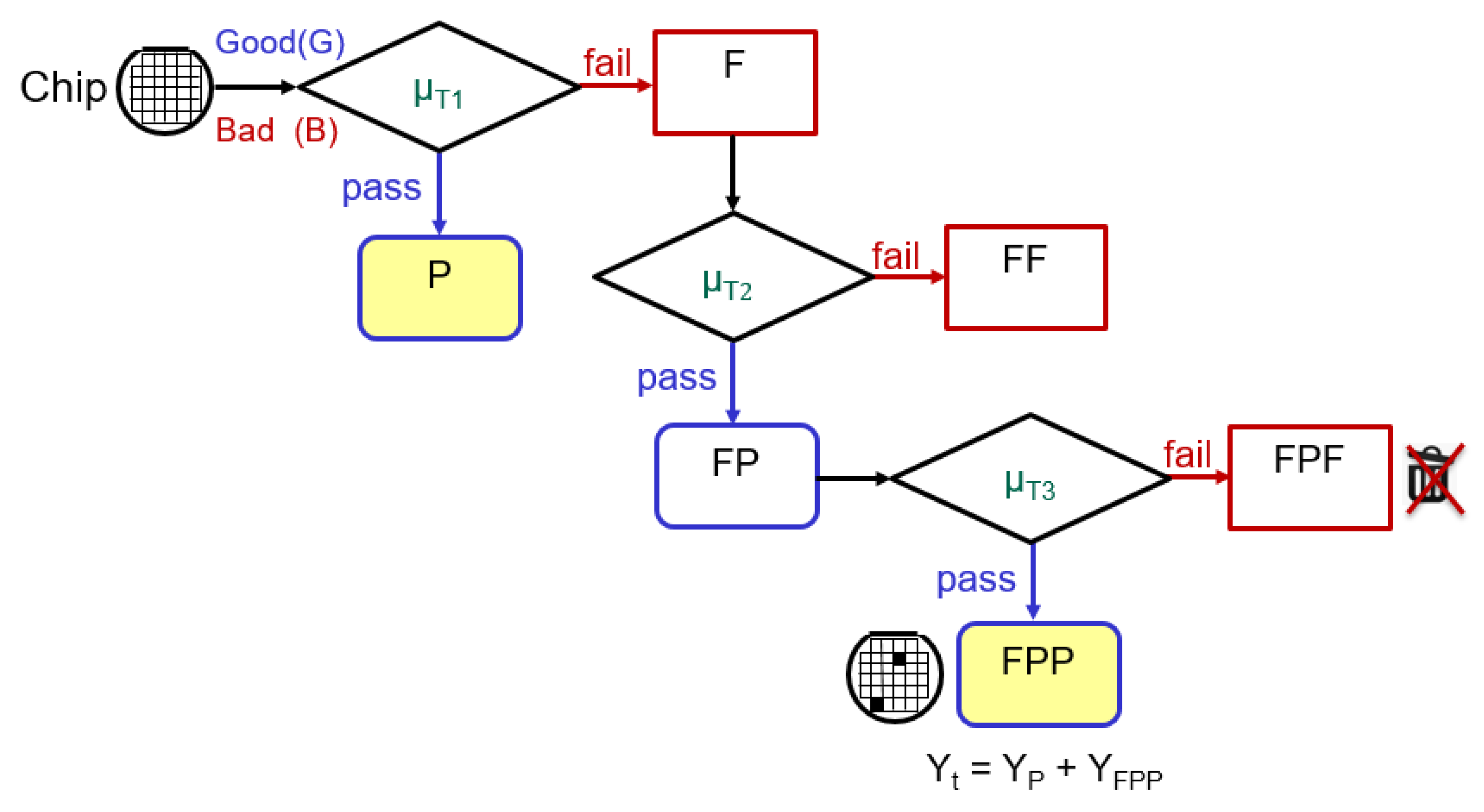
The proposed process is shown in the decision diagram in Figure 4. From the initial test processing, all tested chips are partitioned into pass (P) and fail (F) groups. The bad (F) parts are retested, and the FP parts (those bad chips that pass the first retest) are reserved to be retested again. From this third test, only the FPP parts (those previously failed chips that passed the second and third rounds) are reserved. We call this method “unbalance testing,” a triple-test () scheme [1,2,3,4], and the () formula is defined as
4.1. Use Multiple Test Specifications to Change Test Results
As presented in Table 2, the design specification (DS) was 1165 ps (0.86 GHz), and the circuit characteristic parameter is X~N (x; μM = 1000 ps, σM = 100 ps). According to the above-mentioned data, 95% of Ym could be obtained. In this case, the ATE characteristic parameter (OTA = 120 ps) was used for testing. When we used traditional test methodology , it resulted in a test point set to μT = 1082 ps, and Yt = 77.8%. Next, if we use the unbalanced test method to test the DUT (Figure 4) and use the TS (μT1 = 1083 ps, μT2 = 1100 ps and, μT3 = 1101 ps). Following the previously expressed procedure, the rate of increase in the test yield is as follows: − = 83.24% − 77.8% = 5.44%. When we adopt the unbalanced testing method, we extend the test time and test part F twice; then, moving the test guardband area will affect the test yield or test quality. Therefore, to obtain the desired results, the test engineer must choose the appropriate test specifications (TS) to reduce killing errors and improve test yield. Based on the results of the above comparisons, we used multiple TSs to improve the test yield rate and obtain relatively high benefits.
4.2. Test Accuracy (OTA) Impact on Test Yield and Defect Level
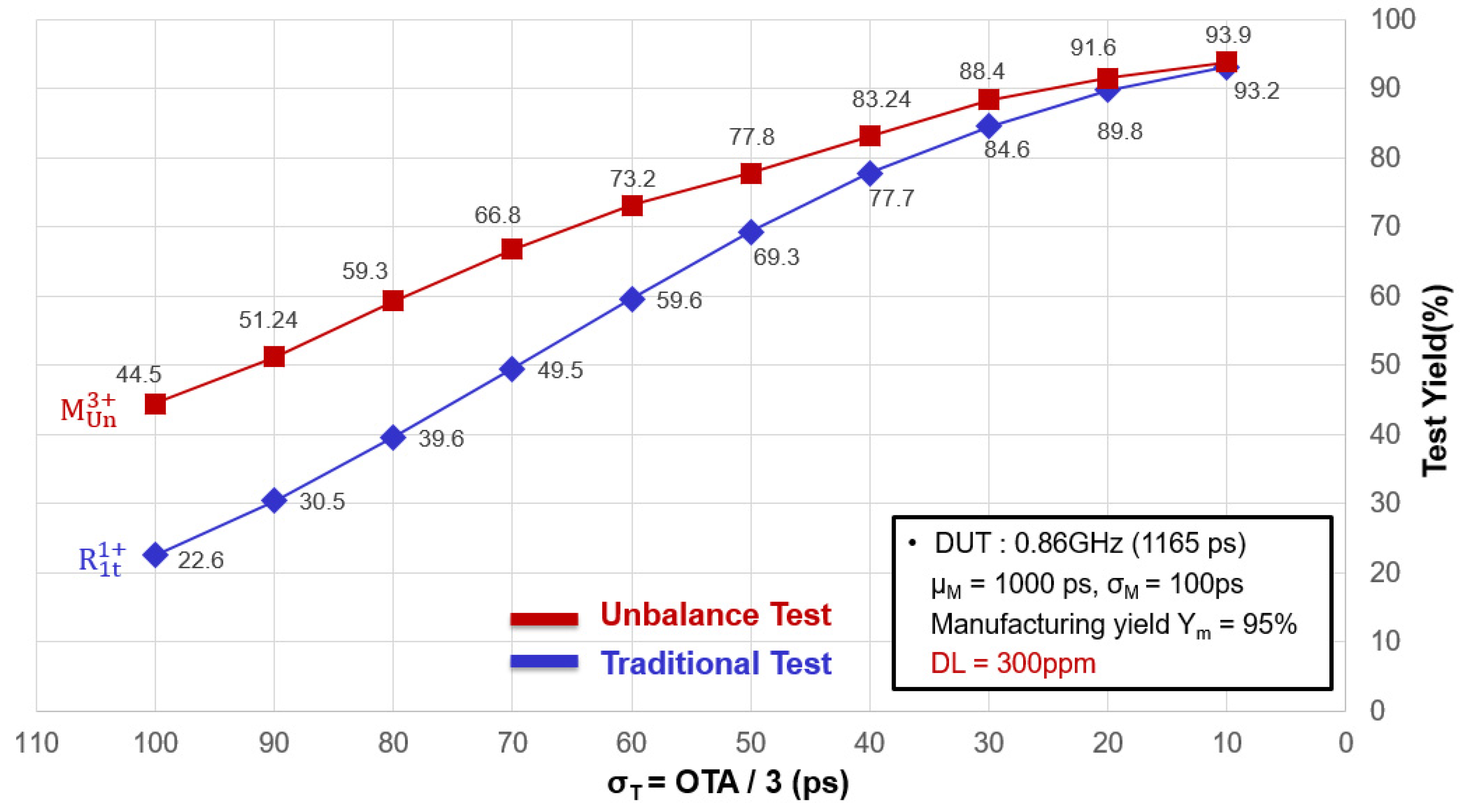
Over the past 30 years, ICs have become increasingly smaller, but their complexity has increased. According to the ITRS roadmap [5,6,7], semiconductors maintain an annual progress rate of 30%. However, ATE maintains an annual improvement rate of 12%. The development speed of the tester is far slower than that of the semiconductor device fabrication. If the trend continues, the inaccuracy of the tester will cause a large loss of yield. Furthermore, several factors affect the test results, such as the tester quality and the TSs (test guardband). In addition to the yield rate, it is also important to choose the appropriate tester. The OTA is the accuracy specification parameter of the tester, which can be used to indicate the tester testability. Here, the test standard deviation, σT, is set to three times that of the OTA. The following example (Figure 5 and Table 3) reveals that smaller the OTA value, the better is the test capability, and a high test quality yield rate can be obtained. Conversely, when the OTA value is larger, the test quality and yield will decrease. This makes the problems of missing and killing errors more serious. However, a high-precision tester will require more testing costs; therefore, test decision-makers should also consider how to choose cost-effective test equipment based on market demand.
For example, a tester of OTA = 60 ps (IC tester with poor testing ability) was used to test the DUT. The traditional test methodology was chosen, and the TS was maintained at 1028 ps; then, Yt was 59.6% and DL was 300 ppm. As time proceeded, the test yield obtained using the traditional test methods worsened, and the drop in test yield is a difficult problem that cannot be avoided. When the TGB was moved and the unbalanced test was adopted for testing, the test yield could be increased to 73.2% (), from 59.6% (). Furthermore, the unbalanced test method was applied to the old tester, and the test method was changed to improve the tester ability. Not only was the unbalanced test method suitable for the old tester equipment, but also it could improve the test yield. When the tester performance increasingly worsens, it means that the test capability is relatively poor compared with the manufacturing capability. Using the unbalanced test method and applying it to the IC test can increase the test yield and afford the company more profits.
5. Applying Unbalanced Testing to the IRDS Table for Guardbanding
In the real world, advances in semiconductor technology occur quickly, so if a testing process lacks current testing abilities [18,19], this may result in a bleak future for the semiconductor industry. To forecast future test yields and test quality, variation in the devices being tested and considerations of the accuracy of the testing process must be considered.
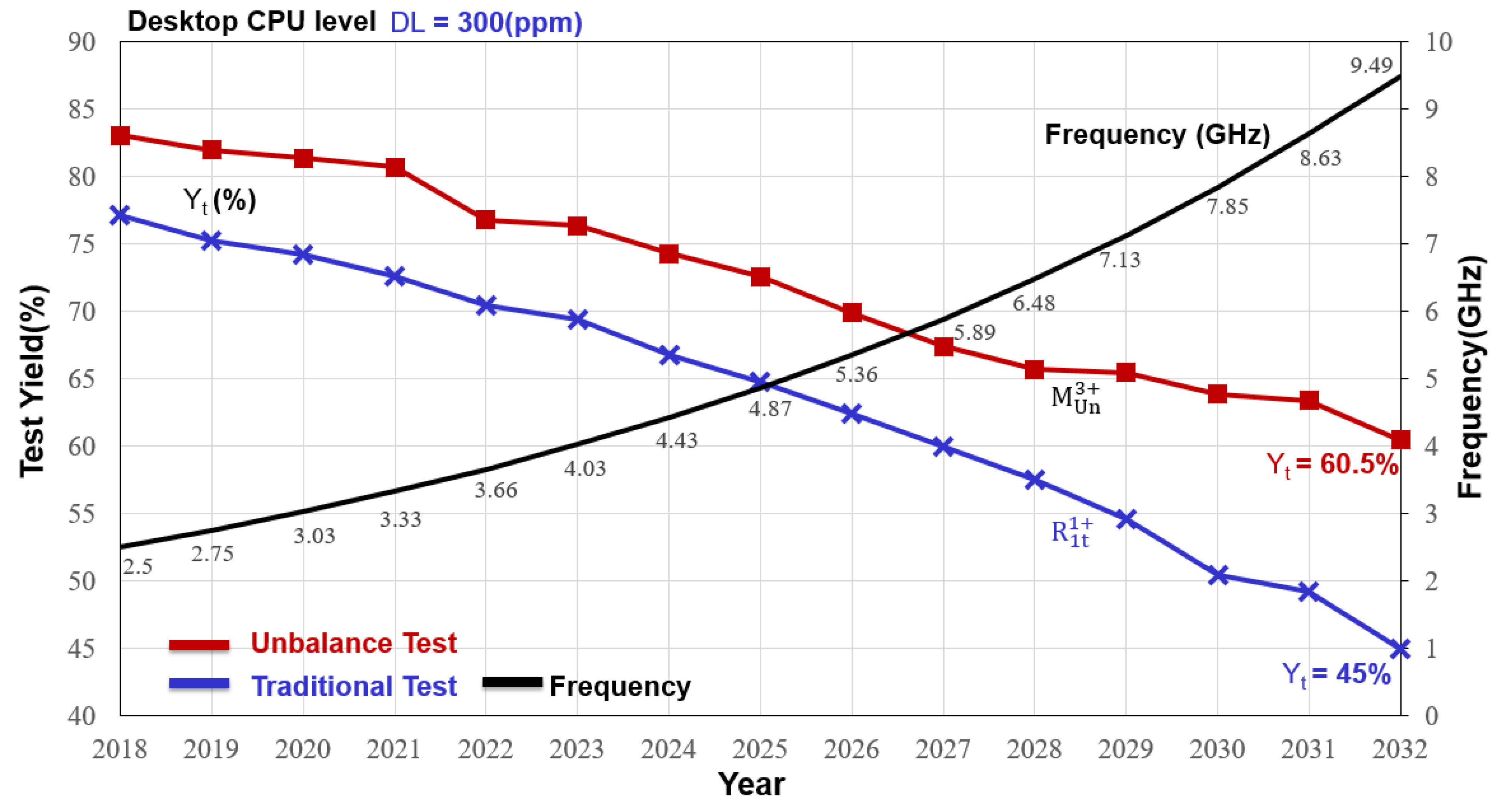
When the traditional test methodology, , is applied to the IRDS (2017) data, according to the forecasting data proposed by the IRDS in 2021 (Figure 6 and Table 4), if a DUT is characterized by X~N (x; 198 ps, 62 ps), the DS is 300 ps. Following the previously expressed procedure, we obtain 95% Ym. The OTA value of the tester (ATE) was stopped at 85.7 ps due to a slow improvement in testability. Here we consider general-quality consumer products, such as the Intel CPU of the desktop personal computer used, and we maintained the DL at 300 ppm and, through iterations of the formula in the traditional functional test, set the test point to 239 ps and the test yield at 72.6%. From the above simulation data, we can find that due to the tester inaccuracy, when the traditional functional testing methods are used, the test pass rate trend deteriorates over time. To promote the test yield, a valid unbalanced testing method, , is proposed, wherein guardband testing is moved to extend the test period. When the unbalanced testing, , and three different μT values (μT1 = 238 ps, μT2 = 257 ps, and μT3 = 258 ps) were used, the test yield could be promoted from to 80.7%, from 72.6%.
The unbalanced test, , promoted the resulting test yield (Yt), which was 8.1% (80.7% − 72.6% = 8.1%) higher than the test yield calculated using the traditional test methodology, . Therefore, when customers demand a higher yield, a higher test frequency using the guardband test adjustment method may improve the yield performance [20,21,22]. Furthermore, when the former calculation was used to estimate the test yield obtained in 2023, employing a testing device whose OTA was 77.4 ps along with the traditional test methodology () to test chips produced in 2023, the test yield dropped to 69.4%. When the unbalanced testing method, , was used under the same conditions, the test yield estimated in 2023 could be improved to 76.4%. These simulation results are presented in Table 4; this shows that the use of repeated testing methods while relaxing the TS can effectively improve the test yield (Yt) without sacrificing the test quality. The higher the test frequency, the fewer the chips that cause killing errors; therefore, the test yield was increasingly improved year by year. With more time spent on testing, chips with killing error could be retrieved, and high yield delivery could be achieved, which together can substantially increase a company’s total profit.
In other words, to improve test yields and test quality, the test conditions and methods were changed, and the test time was extended. Figure 6 shows that the guardband test was moved, and different TS values were used as the basis; then the disqualified chips were tested twice. Thus, the overall yield will improve because of the higher test frequency under the same test quality standard; that is, the part that did not pass the test was tested using repeat testing to minimize the killing error; thus, a bit of quality and time will be sacrificed to promote product yield. As a result, under the same TS parameter conditions, the test guardband (considering product quality) was adjusted, and the test frequency and test time were increased, where the test time and test yield could be exchanged to promote the test yield.
Use of Unbalanced-Test Methods to Improve Test Quality without Sacrificing Test Yield
In the past, the chips of consumer electronics products did not have high-quality requirements. Take the Intel CPU and DDR4 of desktop personal computers as examples, customers sometimes might have bought the defect rate DL (Defect Level) = 200~300 ppm (part per million). This defect rate should be acceptable for both manufacturers and consumers. However, some products such as automotive electronics, biomedical electronics and avionics require higher standards.
Zero-defect and high-quality products are the ultimate goal pursued by all industries. As cars become more modern, the demand for automotive chips also become higher. Products such as controlling the engine, airbag, communication system, ABS (anti-lock braking system), etc., all require the integration and control of the chip. Moreover, a car has a service life of at least 5 to 15 years. This extensive length of service life suggests that the life cycle of the chip used in the car must last much longer than the life cycle of chips in ordinary consumer products. Therefore, high reliability and very strict product certification are required.
Moreover, with the revolution of the automobile industry, the use of electric vehicles has increased significantly. The electrification of the power system of electric vehicles has resulted in significant changes to the power system of vehicles. The power system must be fully monitored and coordinated with a very stable chip to integrate and control such a complex control system (braking system, traction control system, active stability control system, and power system). Therefore, for some critical chip parts, suppliers will even try to reduce the defect rate from the commonly used parts per million (Parts Per Million, PPM) unit to one part per billion (Parts Per Billion, PPB). The reduction of defect rate of the chip can also reduce the malfunction rate of electronic parts and improve driving safety. To ensure that automotive electronic products meet the high standards of operating temperature, durability, and reliability, semiconductor manufacturers have proposed some effective testing and verification methods to reduce the possibility of releasing bad chips into the automotive market.
For example, the American Automotive Electronics Council (AEC) has developed a general method AEC-Q001 [21], which uses the technique of part average testing to remove abnormal parts from the total parts, improve the quality of components, and increase product reliability. However, in the past 30 years in the semiconductor industry, testing and manufacturing technologies have developed at different speeds. Semiconductor testing technology is far behind design and manufacturing technologies, and the quality of products measured is significantly worsening. Here, we change the test decision-making method, adopt the unbalanced-test method to test the device, and reduce the missing errors of the product to achieve high-quality test standards by moving the test guardband.
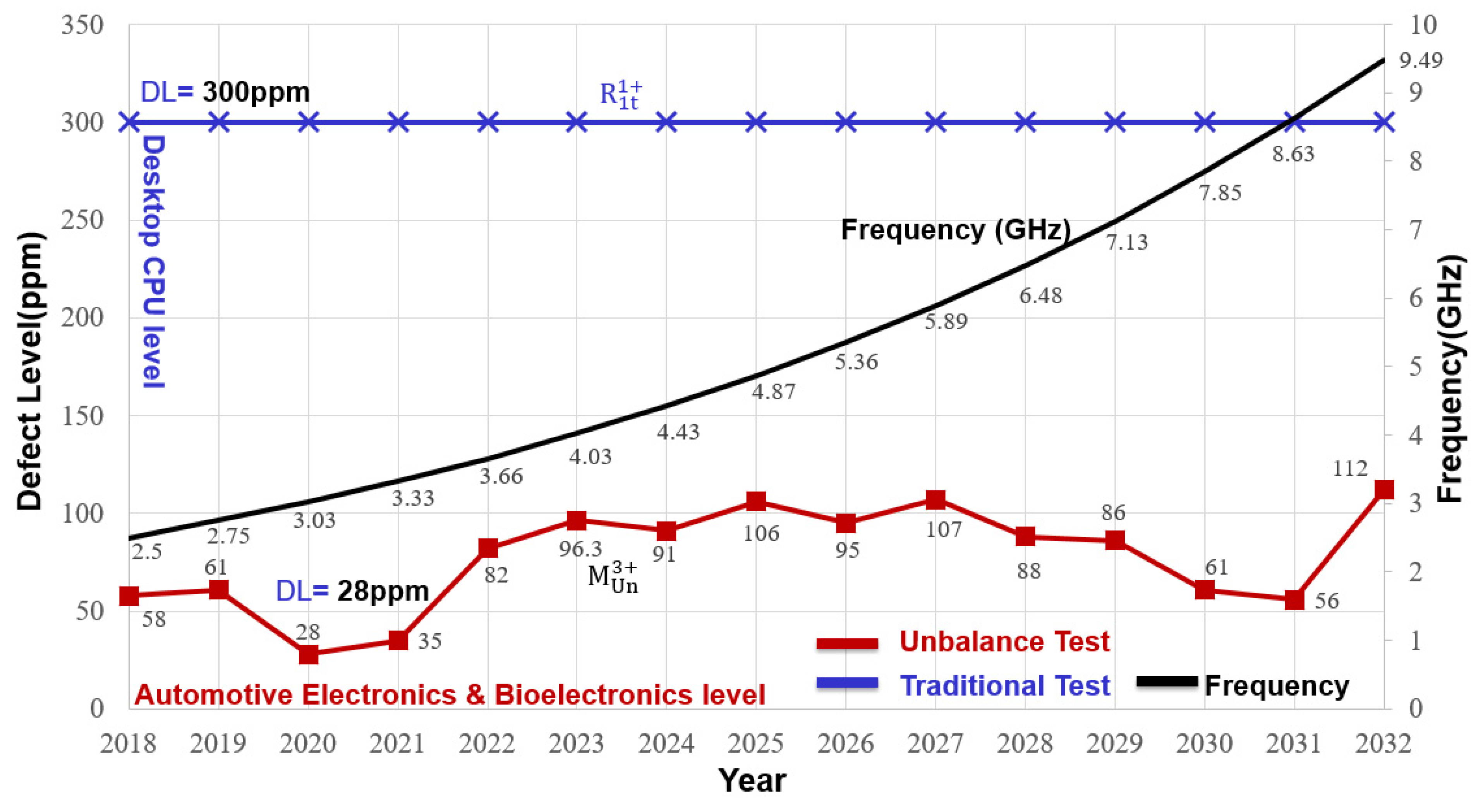
For example, when we used the traditional test methodology, it resulted in a test point set to μT = 266.3 ps, Yt = 74.2%, and DL = 300 ppm in 2020 (Figure 7). When we applied the unbalanced testing to the DUT under the same test yield conditions, the yield of the chips produced in 2020 could be raised to DL = 28 ppm (μT1 = 265 ps, μT2 = 284 ps, and μT3 = 285 ps). Unbalanced testing raised the resulting DL almost by 272 ppm (300 ppm–28 ppm = 272 ppm) compared with the traditional test methodology. Thus, an acceptable Yt and higher quality were obtained with stricter TS. The wider the test guardband range, the higher the promised quality of delivered goods. In other words, although the unbalance test method is time consuming, the DUT is estimated by recursive testing, the occurrence of killing errors and missing errors is reduced, and high-quality chips are effectively selected to achieve the goal of high-quality, near-zero-defect products [23,24,25].
In the past, the chips of consumer electronic products did not have high-quality requirements. However, the functions of the chips of smart electric vehicles are becoming more and more complex, and the quality requirements are high. We all know that the same chip can be applied to different circuit boards and Control complex telecommunications signals. Using an effective unbalance test method, high-quality (5 ppm) IC chips can be classified for use in automotive electronics after testing and classification. At the same time, IC chips with a quality of 300 ppm can be classified as consumer electronics after testing and classification. This effective test method can improve the test yield and increase the company’s profit. On the other hand, under the consideration of product quality, using our proposed test method, different quality chips can be operated in a circuit environment with different functions. It can increase the availability of chips and mitigate the shortage of chips in the supply chain. This effective test method can not only improve the test yield but also increase the company’s profit. In addition, after key components (Automotive electronics and biomedical electronics) have undergone effective product testing, the product quality defect rate unit can be reduced from a few parts per million (PPM) to a few parts per billion (PPB). With the reduction of defect rate of chips and the improvement of the quality of wafers, the safety of car driving has also been enhanced.
6. Conclusions
In this study, a digital integrated-circuit testing model (DITM) is proposed to describe a testing process using test errors to express numerous and complex interrelated IC or chip manufacturing and testing parameters. We digitally analyzed IC yield and quality using normal probability distributions of product properties, introduced testing thresholds and guardbands, and assessed the influence of various parameters on outcomes. Further, we used the digital integrated-circuit test model combined with the existing manufacturing technology and the electrical performance of existing products to estimate the future distribution trend of IC products. The development speeds of IC manufacturing and design technologies are different, and the progress of the design technology is slow and significantly lags behind that of the manufacturing technology. Therefore, if future testing methods for semiconductor products remain unchanged, the test yield will change due to inaccurate testing of new products.
Conversely, the COVID-19 pandemic has recurred and several factories of semiconductor companies have closed or ceased production, with chip production being stalled. Automakers and the consumer market will face reshuffles as they seek short-term solutions to alleviate the chip shortage. Semiconductor industries with stagnant production capacity are due to market constraints and limited production capacity. Thus, finding additional available high-quality chips has become an important issue. Therefore, we proposed the unbalance testing test method, which uses the test guardband to extend the test time, increase the available chips, reduce the killing error chips, and solve some global chip shortages. We used a set of parameters from the 2017 IRDS to demonstrate the proposed unbalance testing, a triple-test scheme, and to show that the test yield can be improved while attaining the desired quality. At the same time, when the test guardband is moved and the device under test (DUT) to be tested is retested several times, the product quality can be improved, and the goal of close to zero defects can be achieved. As long as testing house vendors are willing to spend more time on testing, not only would the chips with killing errors be removed from the defect pile, but a high yield delivery could also be obtained, along with increases in the total profit margin for the company.
Author Contributions
Conceptualization, J.-E.C.; methodology, J.-E.C.; software, C.-H.Y.; validation, C.-H.Y.; formal analysis, C.-H.Y.; investigation, C.-H.Y.; resources, C.-H.Y.; data curation, C.-H.Y.; writing—original draft preparation, C.-H.Y.; writing—review and editing, C.-H.Y.; visualization, J.-E.C.; supervision, C.-H.Y.; project administration, J.-E.C.; funding acquisition, J.-E.C. All authors have read and agreed to the published version of the manuscript.
Funding
This research received no external funding.
Data Availability Statement
All data are included within manuscript.
Acknowledgments
The author would like to thank Jwu E Chen for his invaluable contribution in both defining the model and implementing it mathematically, Inc. for their kind inputs to the model.
Conflicts of Interest
The authors declare no conflict of interest.
References
- Yeh, C.H.; Chen, J.E. Multiple Tests for Maximizing the Yield without Degrading Quality. In Proceedings of the VLSI Test Technology Workshop, Nantao, Taiwan, 15–17 July 2009; pp. 76–81. [Google Scholar]
- Yeh, C.H.; Chen, J.E. Repeated Testing Applications for Improving the IC Test Quality to Achieve Zero Defect Product Requirements. J. Electron. Test. 2019, 35, 459–472. [Google Scholar] [CrossRef]
- Yeh, C.H.; Chen, J.E. The Decision Mechanism Uses the Multiple-Tests Scheme to improve Test Yield in IC Testing. In Proceedings of the International Test Conference in Asia, ITC-Asia 2020, Taipei, Taiwan, 23–25 September 2020; pp. 23–25. [Google Scholar]
- Yeh, C.H. Iterative Estimation of Time-Variant Manufacturing Processes for Test Improvement. Ph.D. Thesis, National Central University, Taiwan, 2020. Available online: https://hdl.handle.net/11296/p8zhe5 (accessed on 23 November 2021).
- International Technology Roadmap for Semiconductors, Test and Test Equipment. 1999, pp. 61–62. Available online: http://cva.stanford.edu/classes/cs99s/papers/roadmap1999.pdf (accessed on 23 May 2019).
- International Technology Roadmap for Semiconductors, Test and Test Equipment. 2001, pp. 5–6. Available online: http://www.itrs2.net/itrs-reports.html (accessed on 1 December 2021).
- International Technology Roadmap for Semiconductors 2.0., System Integration. 2015, pp. 7–13. Available online: http://www.itrs2.net/itrs-reports.html (accessed on 1 December 2021).
- Dalal, W.; Miao, S. The Value of Tester Accuracy. In Proceedings of the International Test Conference 1999, Atlantic City, NJ, USA, 30–30 September 1999; pp. 518–523. [Google Scholar]
- West, B.G. Accuracy requirements in at-speed functional test. In Proceedings of the International Test Conference 1999, Atlantic City, NJ, USA, 30–30 September 1999; pp. 780–787. [Google Scholar]
- The IEEE International Roadmap for Devices and Systems Table; 2017 Edition. pp. 18–23. Available online: https://0-irds-ieee-org.brum.beds.ac.uk/images/files/pdf/2017/2017IRDS_MM.pdf (accessed on 1 December 2021).
- Williams, R.H.; Hawkins, C.F. The Economics of Guardband Placement. In Proceedings of the IEEE International Test Conference-(ITC), Baltimore, MD, USA, 17–21 October 1993; pp. 218–225. [Google Scholar]
- Chen, J.E.; Yeh, C.H. Test Guardbanding for Yield and Quality Estimation. In Proceedings of the International Test Synthesis Workshop (ITSW 2009), Austin, TX, USA, 23–25 March 2009; pp. 114–115. [Google Scholar]
- Jang, S.I.; Lee, J.H. An Automated Retesting Approach for Wafer Probing Test Systems Using Neural Networks. In Proceedings of the World Congress on Engineering and Computer Science Vol II (WCECS 2011), San Francisco, CA, USA, 19–21 October 2011; pp. 1058–1063. [Google Scholar]
- Horng, S.C.; Lin, S.Y.; Cheng, M.H.; Yang, F.Y.; Liu, C.H.; Lee, W.Y.; Tsai, C.H. Reducing the overkills and retests in wafer testing process. In Proceedings of the Advanced Semiconductor Manufacturing Conference and Workshop (IEEEI/SEMI 2003), Munich, Germany, 31 March–1 April 2003; pp. 286–291. [Google Scholar] [CrossRef]
- Jena, S.K.; Biswas, S.; Deka, J.K. Maximizing Yield through Retesting of Rejected Circuits using Approximation Technique. In Proceedings of the 2020 IEEE REGION 10 CONFERENCE (TENCON 2020), Osaka, Japan, 16–19 November 2020; pp. 182–187. [Google Scholar] [CrossRef]
- Chang, P.; Huang, Y.K. Intelligent Method for Retesting a Wafer; Teslence Technology Co., Ltd.; Available online: https://www.swtest.org/swtw_library/2019proc/PDF/S02_02_Chang_SWTest_2019.pdf (accessed on 3 April 2021).
- Lin, W.; Shi, W.L. An on-Chip Clock Controller for Testing Fault in System on Chip. In Proceedings of the 2nd International Conference on Computer Science and Electronics Engineering (ICCSEE 2013), Hangzhou, China, 22–23 March 2013; pp. 347–350, 724. [Google Scholar]
- Fisher, P.D.; Nesbitt, R. The Test of Time: Clock-Cycle Estimation and Test Challenges for Future Microprocessors. IEEE Circuits Devices Mag. 1998, 14, 37–44. [Google Scholar] [CrossRef]
- Williams, R.H.; Wagner, R.G.; Hawkins, C.F. Testing Errors: Data and Calculations in an IC Manufacturing Process. In Proceedings of the International Test Conference 1992, Baltimore, MD, USA, 20–24 September 1995; pp. 352–361. [Google Scholar]
- AEC-Q004, Zero Defects Guideline. 2006, pp. 18–23. Available online: http://www.aecouncil.com/AECDocuments.html (accessed on 1 December 2021).
- AEC-Q001-REV-C, Guidelines for Part Average Testing. 2003, pp. 3–7. Available online: http://www.aecouncil.com/AECDocuments.html (accessed on 1 December 2021).
- Nigh, P. Achieving quality levels of 100 DPM: It’s possible... but roll up your sleeves and be prepared to do some work. In 2004 International Conferce on Testt; IEEE Computer Society: Washington, DC, USA, 2004; pp. 26–28. [Google Scholar]
- Madge, R.; Benware, B.; Ward, M.; Daasch, R. The value of statistical testing for quality, yield and test cost improvement. In IEEE International Conference on Test; IEEE Computer Society: Washington, DC, USA, 2005. [Google Scholar]
- Raina, R. Achieving Zero-Defects for Automotive Applications. In Proceedings of the 2008 IEEE International Test Conference, Santa Clara, CA, USA, 28–30 October 2008. [Google Scholar]
- Bedsole, J.; Raina, R.; Crouch, A.; Abadir, M.S. Very low cost testers: Opportunities and challenges. IEEE Des. Test Comput. 2001, 18, 60–69. [Google Scholar] [CrossRef]
Figure 1.
Very−large−scale integration VLSI chip development procedures.

Figure 2.
Product manufacturability impact on manufacturing yield.

Figure 3.
Influence of test guardband on test yield and test quality.

Figure 4.
Proposed decision diagram for unbalanced testing ().

Figure 5.
The impact of test parameter OTA on test results.

Figure 6.
Methods used to estimate the test yield in future products.

Figure 7.
Methods used to estimate the test quality under same test yield conditions.


Table 1.
IEEE International Roadmap for Devices and Systems (2017 Edition).
| Year | Unit | 2018 | 2019 | 2020 | 2021 | 2022 | 2023 | 2024 | 2025 | 2026 | 2027 | 2028 | 2029 | 2030 | 2031 | 2032 |
|---|---|---|---|---|---|---|---|---|---|---|---|---|---|---|---|---|
| Chip frequency | GHz | 2.5 | 2.75 | 3.03 | 3.33 | 3.66 | 4.03 | 4.43 | 4.87 | 5.36 | 5.89 | 6.48 | 7.13 | 7.85 | 8.63 | 9.49 |
| Device period | ps | 400 | 354 | 330 | 300 | 273 | 248 | 226 | 205 | 187 | 170 | 154 | 140 | 127 | 116 | 105 |
| μM | ps | 264 | 233 | 218 | 198 | 180 | 163 | 149 | 135 | 123 | 112 | 101 | 92 | 84 | 76 | 69 |
| σM | ps | 83 | 73 | 68 | 62 | 57 | 51 | 47 | 42 | 39 | 35 | 32 | 29 | 26 | 24 | 22 |
Table 2.
Test results for different test specifications and methods.
| Test Method | TS (ps) | Yt (%) | DL (ppm) |
|---|---|---|---|
| (YP + YFPP) | TS (μT1) = 1083 TS (μT2) = 1100 TS (μT3) = 1101 | 83.24 | 300 |
| TS (μT) =1082 | 77.8 | 300 |
Table 3.
Unbalance testing methods enhance the testing capabilities of the tester.
| σT = OTA/3 | ps | 10 | 20 | 30 | 40 | 50 | 60 | 70 | 80 | 90 | 100 | |
|---|---|---|---|---|---|---|---|---|---|---|---|---|
| TS (μT) | ps | 1150 | 1129 | 1107 | 1082 | 1056 | 1028 | 999 | 966 | 931 | 894 | |
| Yt | % | 93.2 | 89.8 | 84.6 | 77.8 | 69.3 | 59.6 | 49.5 | 39.6 | 30.5 | 22.6 | |
| TS (μT1) | ps | 1147 | 1126 | 1104 | 1083 | 1056 | 1025 | 990 | 960 | 931 | 885 | |
| TS (μT2) | 1157 | 1138 | 1124 | 1100 | 1079 | 1075 | 1060 | 1040 | 1022 | 1011 | ||
| TS (μT3) | 1158 | 1149 | 1128 | 1101 | 1090 | 1085 | 1077 | 1060 | 1033 | 1023 | ||
| Yt | % | 93.9 | 91.6 | 88.4 | 83.24 | 77.8 | 73.2 | 66.8 | 59.3 | 51.24 | 44.5 | |
| DL | ppm | 300 | 300 | 300 | 300 | 300 | 300 | 300 | 300 | 300 | 300 |
Table 4.
Comparison of yields and qualities obtained by two test methods (IRDS 2017).
| Year | Unit | 2018 | 2019 | 2020 | 2021 | 2022 | 2023 | 2024 | 2025 | 2026 | 2027 | 2028 | 2029 | 2030 | 2031 | 2032 | |
|---|---|---|---|---|---|---|---|---|---|---|---|---|---|---|---|---|---|
| Chip frequency | GHz | 2.5 | 2.75 | 3.03 | 3.33 | 3.66 | 4.03 | 4.43 | 4.87 | 5.36 | 5.89 | 6.48 | 7.13 | 7.85 | 8.63 | 9.49 | |
| Device period | ps | 400 | 354 | 330 | 300 | 273 | 248 | 226 | 205 | 187 | 170 | 154 | 140 | 127 | 116 | 105 | |
| μM | ps | 264 | 233 | 218 | 198 | 180 | 163 | 149 | 135 | 123 | 112 | 101 | 92 | 84 | 76 | 69 | |
| σM | ps | 83 | 73 | 68 | 62 | 57 | 51 | 47 | 42 | 39 | 35 | 32 | 29 | 26 | 24 | 22 | |
| OTA | ps | 100 | 95 | 90.25 | 85.7 | 81.5 | 77.4 | 73.5 | 70 | 66.3 | 63 | 59.9 | 56.9 | 54 | 51.3 | 48.8 | |
| TS (μT) | ps | 330.7 | 287.5 | 266.3 | 239 | 214 | 192 | 172 | 153.3 | 137.2 | 122.3 | 108.1 | 96 | 84.4 | 75.4 | 65.5 | |
| Yt | % | 77.2 | 75.3 | 74.2 | 72.6 | 70.5 | 69.4 | 66.8 | 64.8 | 62.4 | 60 | 57.5 | 54.6 | 50.5 | 49.2 | 45 | |
| DL | ppm | 300 | 300 | 300 | 300 | 300 | 300 | 300 | 300 | 300 | 300 | 300 | 300 | 300 | 300 | 300 | |
| TS (μT1) | ps | 330 | 287 | 265 | 238 | 214.8 | 192.7 | 172.7 | 154 | 138 | 123 | 109 | 99 | 85.2 | 76 | 66.3 | |
| TS (μT2) | 349 | 304 | 284 | 257 | 220 | 198 | 178 | 158 | 140 | 124 | 111 | 101 | 91 | 82 | 77 | ||
| TS (μT3) | 348 | 305 | 285 | 258 | 221 | 201 | 181 | 161 | 142 | 126 | 112 | 102 | 101 | 93 | 78 | ||
| Yt | % | 83.1 | 82 | 81.4 | 80.7 | 76.8 | 76.4 | 74.3 | 72.6 | 69.9 | 67.4 | 65.7 | 65.5 | 63.9 | 63.4 | 60.5 | |
| DL | ppm | 300 | 300 | 300 | 300 | 300 | 300 | 300 | 300 | 300 | 300 | 300 | 300 | 300 | 300 | 300 | |
| TS (μT1) | ps | 311 | 270 | 265 | 217 | 202 | 182 | 162 | 145 | 129 | 115 | 100 | 88 | 75 | 66 | 60 | |
| TS (μT2) | 331 | 286 | 284 | 243 | 209 | 186 | 168 | 148 | 133 | 116 | 105 | 93 | 84 | 72 | 63 | ||
| TS (μT3) | 338 | 287 | 285 | 244 | 210 | 187 | 169 | 147 | 134 | 118 | 107 | 95 | 86 | 83 | 64 | ||
| Yt | % | 77.2 | 75.3 | 74.2 | 72.6 | 70.5 | 69.4 | 66.8 | 64.8 | 62.4 | 60 | 57.5 | 54.6 | 50.5 | 49.2 | 45 | |
| DL | ppm | 58 | 61 | 28 | 35 | 82 | 96.3 | 91 | 106 | 95 | 107 | 88 | 86 | 61 | 56 | 112 | |
Publisher’s Note: MDPI stays neutral with regard to jurisdictional claims in published maps and institutional affiliations. |
© 2021 by the authors. Licensee MDPI, Basel, Switzerland. This article is an open access article distributed under the terms and conditions of the Creative Commons Attribution (CC BY) license (https://creativecommons.org/licenses/by/4.0/).
Share and Cite
MDPI and ACS Style
Yeh, C.-H.; Chen, J.-E. Unbalanced-Tests to the Improvement of Yield and Quality. Electronics 2021, 10, 3032. https://0-doi-org.brum.beds.ac.uk/10.3390/electronics10233032
AMA Style
Yeh C-H, Chen J-E. Unbalanced-Tests to the Improvement of Yield and Quality. Electronics. 2021; 10(23):3032. https://0-doi-org.brum.beds.ac.uk/10.3390/electronics10233032
Chicago/Turabian StyleYeh, Chung-Huang, and Jwu-E Chen. 2021. "Unbalanced-Tests to the Improvement of Yield and Quality" Electronics 10, no. 23: 3032. https://0-doi-org.brum.beds.ac.uk/10.3390/electronics10233032
Note that from the first issue of 2016, this journal uses article numbers instead of page numbers. See further details here.