
A 4 GHz Single-to-Differential Cross-Coupled Variable-Gain Transimpedance Amplifier for Optical Communication


Engineering Product Development, Singapore University of Technology and Design (SUTD), 8 Somapah Road, Singapore 487372, Singapore
*
Author to whom correspondence should be addressed.
Electronics 2021, 10(23), 3042; https://0-doi-org.brum.beds.ac.uk/10.3390/electronics10233042
Submission received: 8 November 2021
/
Revised: 1 December 2021
/
Accepted: 2 December 2021
/
Published: 5 December 2021
(This article belongs to the Special Issue Feature Papers in Circuit and Signal Processing)
Abstract
:This letter presents an inductorless transimpedance amplifier (TIA) for visible light communication, using the UMC 40 nm CMOS process. It consists of a single-to-differential input stage with a modified cross-coupled regulated cascode design, followed by a modified -doubler mid-stage with a combined active inductor and capacitive degeneration design for bandwidth-enhancement and differential output. The mid-stage also has an attached common-mode feedback (CMFB) circuit. Both the input and mid-stages have gain-varying and peaking-varying functions. It has a measured gain range of 37.5–58.7 dBΩ and 4.15 GHz bandwidth using a 0.5 pF capacitive load. The gain range results in an input dynamic range of 33.2 µA–1.46 mA. Its input referred noise current is 10.7 pA/, core DC power consumption is 7.84 mW from a of 1.6 V and core area is 39 µm × 26 µm.
1. Introduction
The popularity of new bandwidth-intensive services such as cloud-computing and the internet of things has increased the demand for high-speed data transmission capability. The current wireless transmission (Wi-Fi) frequency for near-field communication is reaching the saturation limit. Thus, the large, unused visible light spectrum (400–800 THz) is gaining increasing research attention for near-field visible light communication (VLC) [1]. There are several key benefits of VLC. Firstly, VLC is secure as visible light is unable to pass through opaque walls, hence securing in-room data transmission. Secondly, VLC is safe to use in locations where interference of RF signals occurs, such as in hospitals and plane cabins [2]. Thirdly, as the cost of light-emitting diodes (LED) is rapidly decreasing, they are expected to become the dominant form of lighting [3]. As LEDs are able to be driven to transmit data through high-frequency modulated light signals [4,5], this makes widespread VLC adoption highly feasible in the near future.
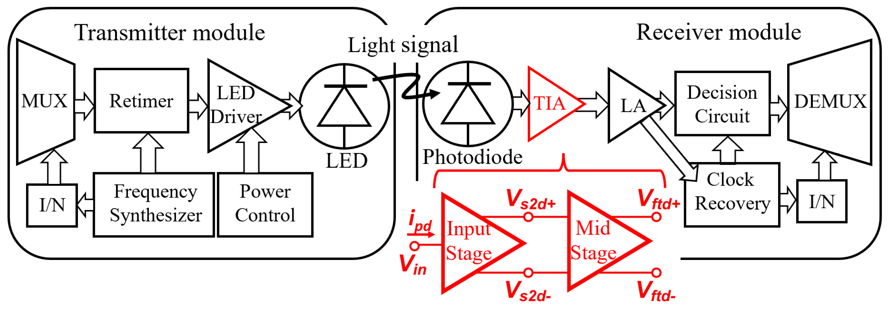
CMOS technology is preferred for chip design as it is cheap, mature and has on-chip photodiode integrability [6,7]. The VLC architecture for the transmitter and receiver is shown in Figure 1 [4,5]. Data are transferred from the transmitter to the receiver through air via a modulated programmed high-frequency flickering light signal using properly driven LEDs. As shown in Figure 1, within the receiver module, the transimpedance amplifier (TIA) is the first chip block and it is the most crucial as it determines the bandwidth, noise and sensitivity for the receiver [7].
Thus, this paper’s objective is the design of a TIA which is the most crucial component for a VLC system, which is expected to become common. The main issue for TIA designs is that the photodiode before the TIA has a capacitive load taken as 0.5 pF [3]. contributes greatly to the dominant pole at the input, limiting bandwidth. Thus, the key TIA trade-off is between transimpedance gain and bandwidth [6]. Many TIA designs counter it by reducing the input impedance [6,7,8].
Regulated cascode (RGC) is a common TIA design to lower [8,9]. Bandwidth-enhancing methods such as capacitive degeneration and inductive peaking are commonly used [4,8]. RGC design can also be modified to use both PMOS and NMOS configurations [10]. A single-to-differential TIA can be performed via cross-coupling [11]. When the distance between the transceiver and receiver is large, needs to be large to amplify the weak input signal. Conversely, when the distance is small, needs to be small to prevent saturation of the input signal. Thus, a gain-varying design with large input dynamic range is desired as varies from 0.15 to 0.9 mA [8,12] for variable link distances [13].
This paper presents a 40 nm CMOS two-stage single-to-differential cross-coupled variable-gain TIA design with analysis of its key features, and it is taped-out and measured. The rest of the paper is organized as follows. Section 2 presents its single-to-differential cross-coupled modified-RGC input stage and Section 3 presents its -doubler mid-stage with combined active inductor and capacitive degeneration. Section 4 presents the layout and die microphotographs, while Section 5 presents the post-layout simulation and measurement results. Section 6 is the discussion and comparison with other recent works, while Section 7 is the conclusion.
2. Input Stage of TIA Design
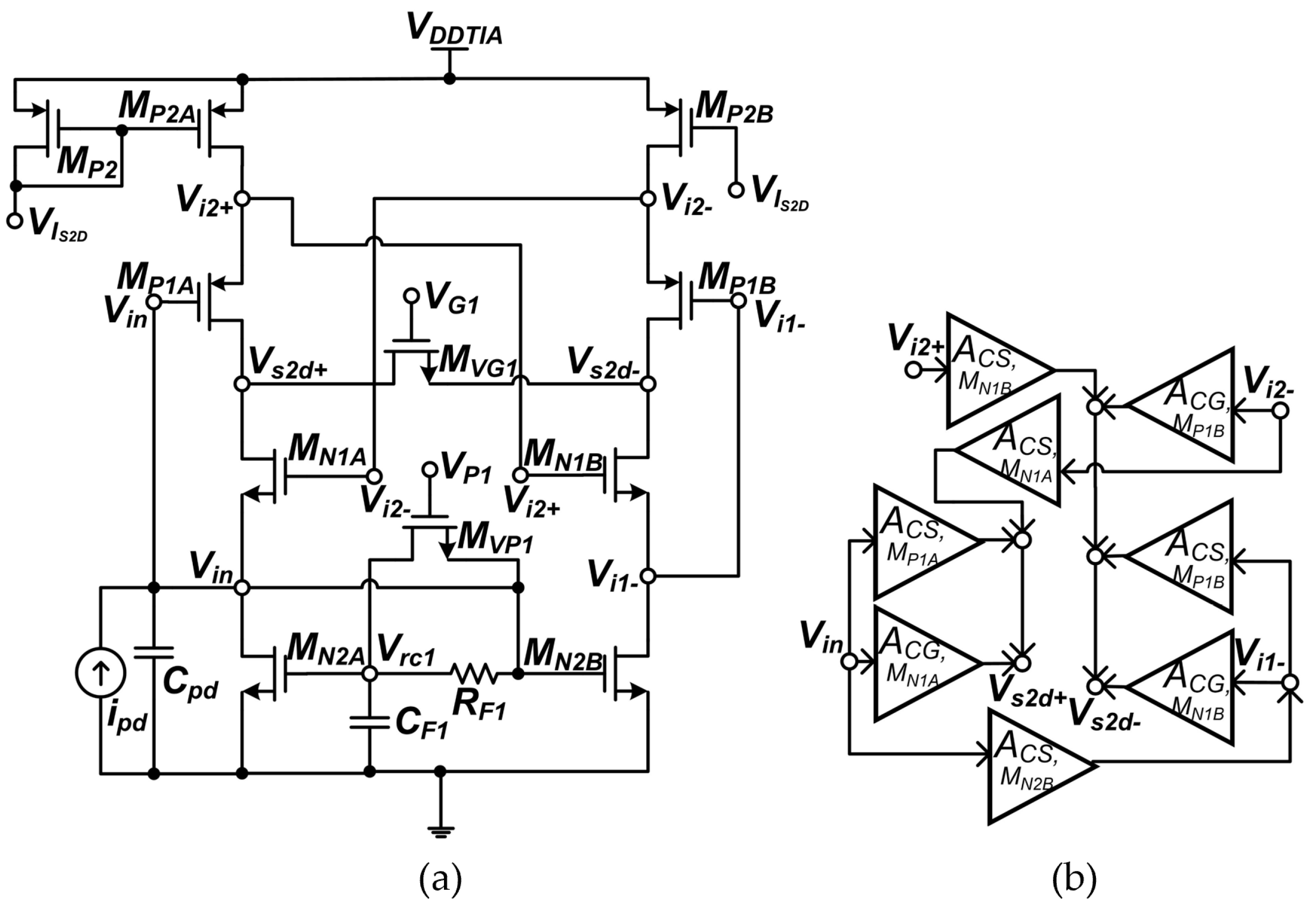
The proposed TIA design is modified from the authors’ simulated fixed-gain design in [7], with no large DC-blocking capacitors at input required here. The input stage schematic is shown in Figure 2a with the input at and outputs at and with its simplified loop diagram in Figure 2b.
2.1. Design Features of the TIA Input Stage
The proposed TIA input stage has some key design features. Firstly, it is differential, unlike in [14], as the component sizes for both sides are equal. The low-pass filters and ensure equal DC biasing of , while current mirrors fix current. Hence, DC at remain equal as the input current varies. Secondly, it has a combined modified-RGC and cross-coupled design. act as both common-gate (CG) and common-source (CS) due to the cross-coupling design [8], giving it both a small CG and large CS gain. The cascode feedbacks to are across which separate and . Thus, this prevents parasitic capacitances of the feedbacks from loading while also allowing widths of to be smaller.
Thirdly, there are both variable-gain and peaking functions which increase the dynamic range upper limit. acts as a variable resistor. When is low, is off. As increases, turns on linearly, reducing gain across . The low-pass filters and also generate a zero that affects the frequency response. When is increased, turns on and the zero shifts, preventing peaking for lower gain settings, making this TIA design suitable for variable VLC conditions.
2.2. Input Impedance and Transimpedance Gain
Input impedance is estimated by taking all components connected to and is calculated as:
where is the transistor output resistance and of , , and are taken to be the same.
The single-ended transimpedance gains of the input stages and are different due to their asymmetrical design. They are estimated by finding and combining gain loop transfer functions, with the simplified diagram shown in Figure 2b. of loops from to and from to are calculated from their respective loop gains to be:
The differential transimepdance gain is equal to .
3. Mid-Stage of TIA Design
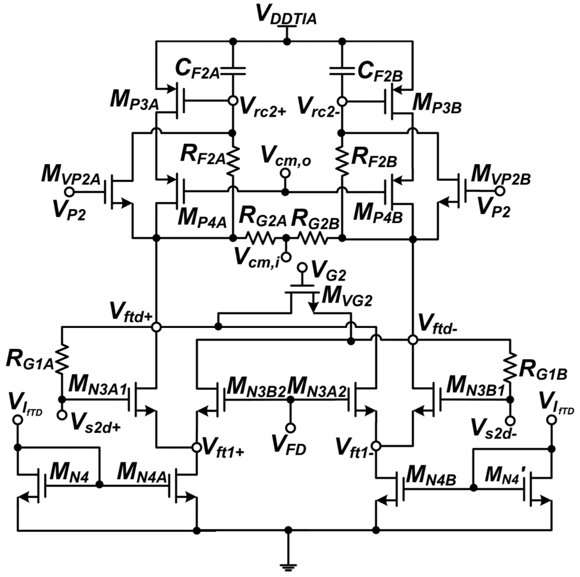
The schematic of the modified (transit frequency) doubler mid-stage is shown in Figure 3.
The mid-stage has additional gain and peaking variation functions and a common-mode feedback (CMFB) circuit as compared to [7]. It makes the differential signal highly ideal while enhancing bandwidth. The inputs of the mid-stage are at and outputs are at .
3.1. Design Features of the TIA Mid-Stage
The -doubler mid-stage also has several design features. Firstly, it halves both the input and output capacitances and gives a more ideal differential signal output at [5,7]. As in Figure 2, the CS amplifiers and drains cross with each other at the outputs ( and ) and ( and ). The transistor sources also combine at and with two current mirrors . This makes the output signal highly differential.
Secondly, there is a combined active inductor and capacitive degeneration design consisting of , and . Both are bandwidth-enhancing techniques that introduce a zero in the gain transfer function, to counter the gain drop-off due to the dominant pole, and thus increase bandwidth. By combining both techniques together into a single unique structure, this reduces circuit area while giving a more prominent zero at , thus increasing the bandwidth even more. Gain and peaking are similarly adjustable and controlled by adjusting / and /, respectively, preventing peaking in the frequency response at any gain setting and thus preventing instability.
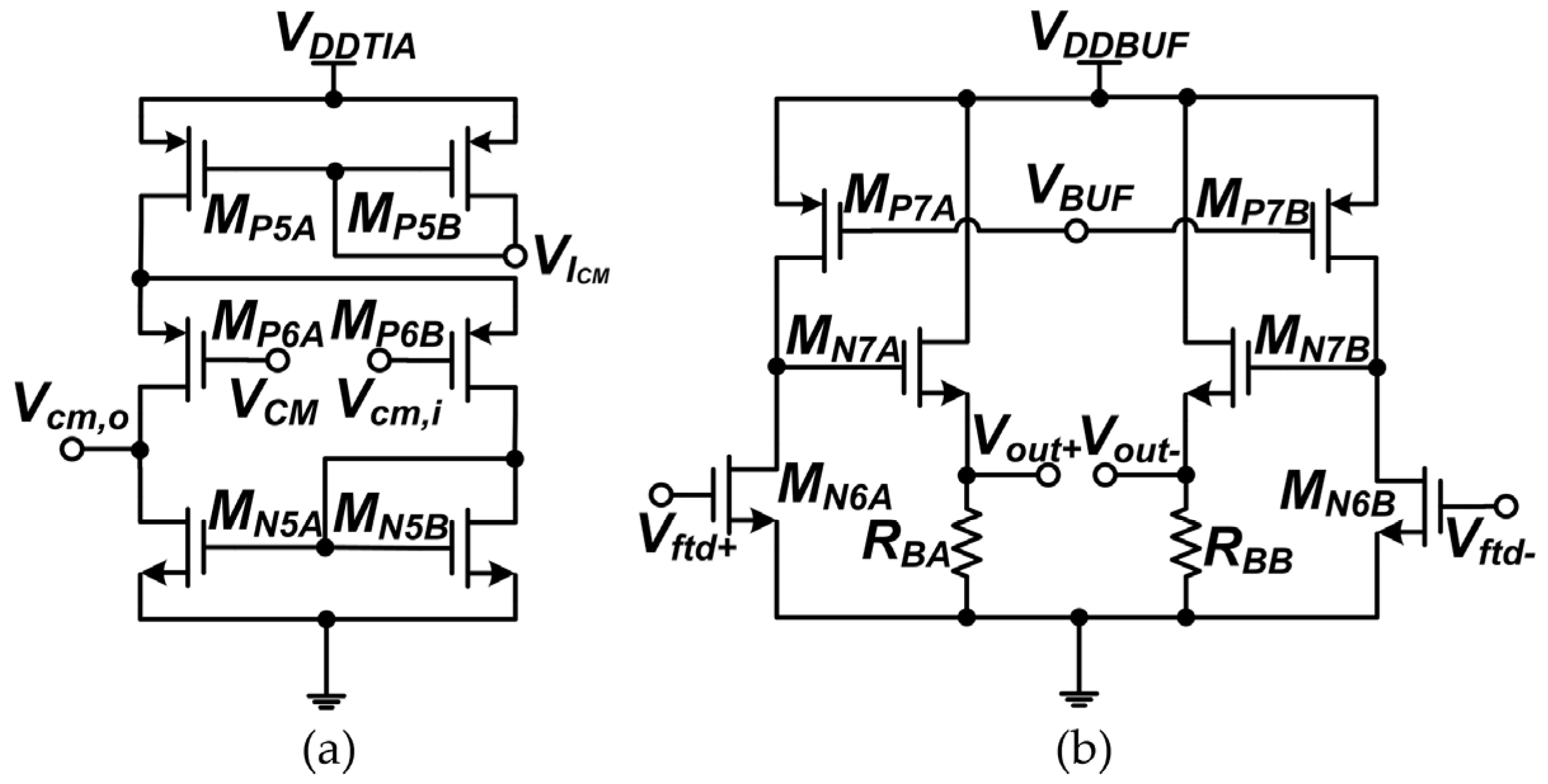
Thirdly, a CMFB circuit is used for differential circuits to prevent common-mode voltage shifts from occurring, which may push transistors out of their normal DC biases [5]. The CMFB circuit in Figure 4a is biased by and , with its input at and output at . is taken from the mid-point of the mid-stage differential outputs while controls in the mid-stage to complete the CMFB loop.
The buffer after the mid-stage in Figure 4b has a common-source that offsets the gain loss of the common-drain , hence making it gain neutral. Its inputs are at and outputs are at .
3.2. Voltage Gain
In the -doubler, are the main common sources that produce voltage gain. Hence, the voltage gain for mid-stage is:
where is the gain impact of the DC-biased .
The differential transimpedance gain of the entire TIA is equivalent to the differential input-stage transimpedance gain multiplied by the gain-stage voltage gain:
4. Layout
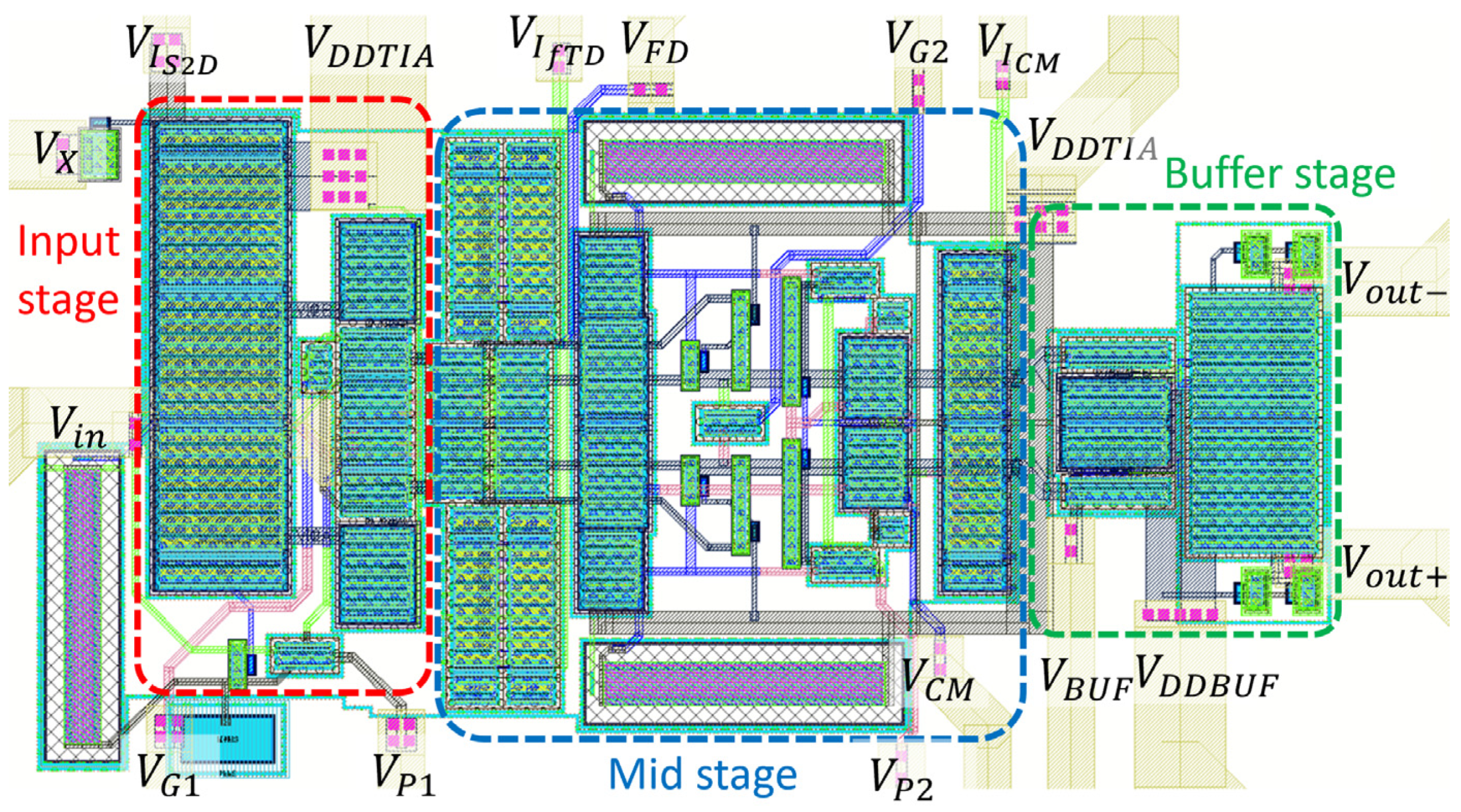
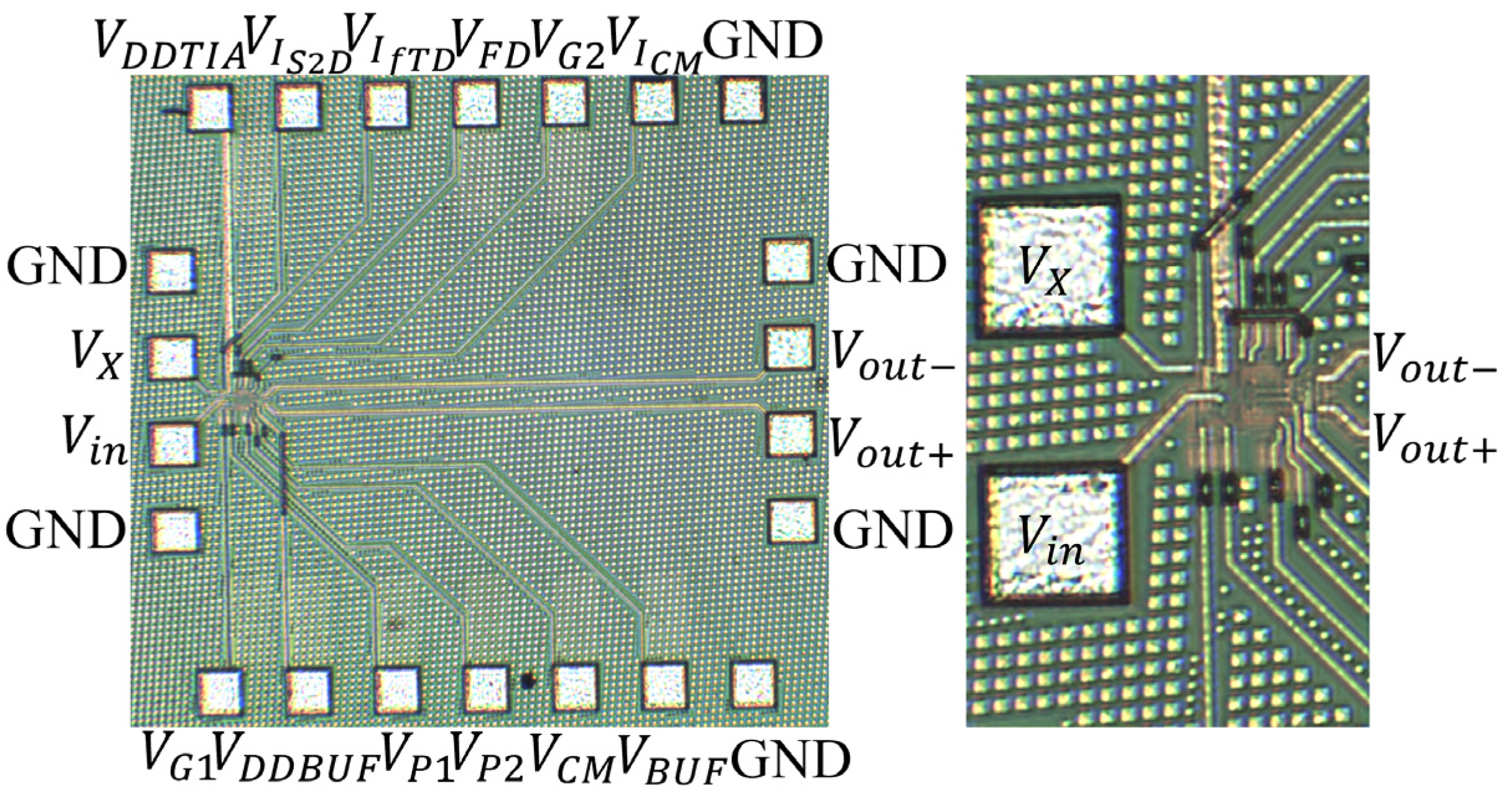
The layout of the proposed TIA is shown in Figure 5 and the die microphotographs are shown in Figure 6. DC biasing values for the TIA are shown in Table 1, as well as the biasings for the variable-gain and peaking settings. There are six TIA gain settings for this design.
The core area (input and mid-stages) of the TIA design is 39 µm × 26 µm.
are variables to control the variable gains and peakings at different gain settings. The measured core TIA power is 7.84 mW and the buffer power is 5.01 mW. A Keysight PNA-X N5247A Network Analyzer was used to measure the S-parameters and IP1dB. PNA port 1 was connected to and ports 2 and 3 to . The pad was not used.
5. Simulation and Measurement Results
5.1. Transimpedance Gain and Bandwidth
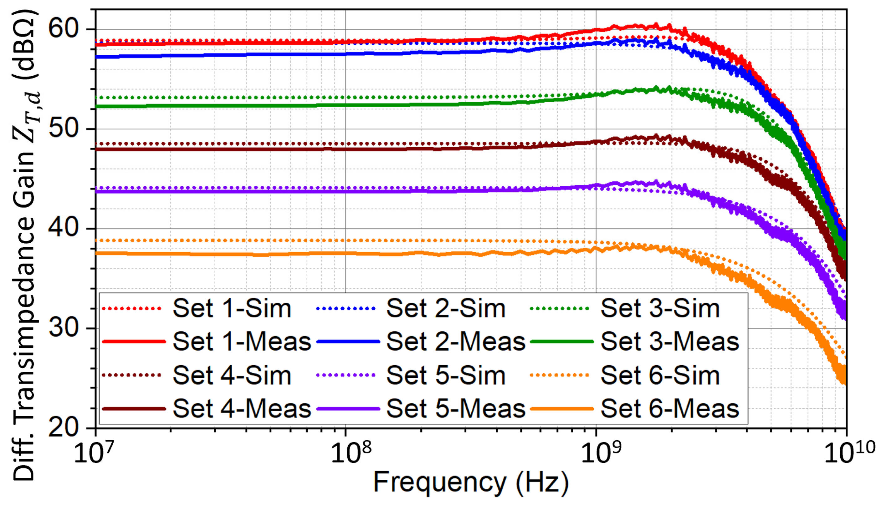
Both the post-layout simulation and measurement results of the proposed TIA differential transimpedance gain frequency response are plotted in Figure 7 at settings 1–6.
The results of the TIA frequency response are in Table 2 below, with taken at 100 MHz and bandwidth at –3 dB of . The measured ranges from 37.5 to 58.7 dBΩ (range of 21.2 dBΩ) across settings 1–6, with bandwidth above 4.15 GHz. The TIA is also stable with limited peaking within the frequency response as shown.
5.2. IP1dB and Gain Compression
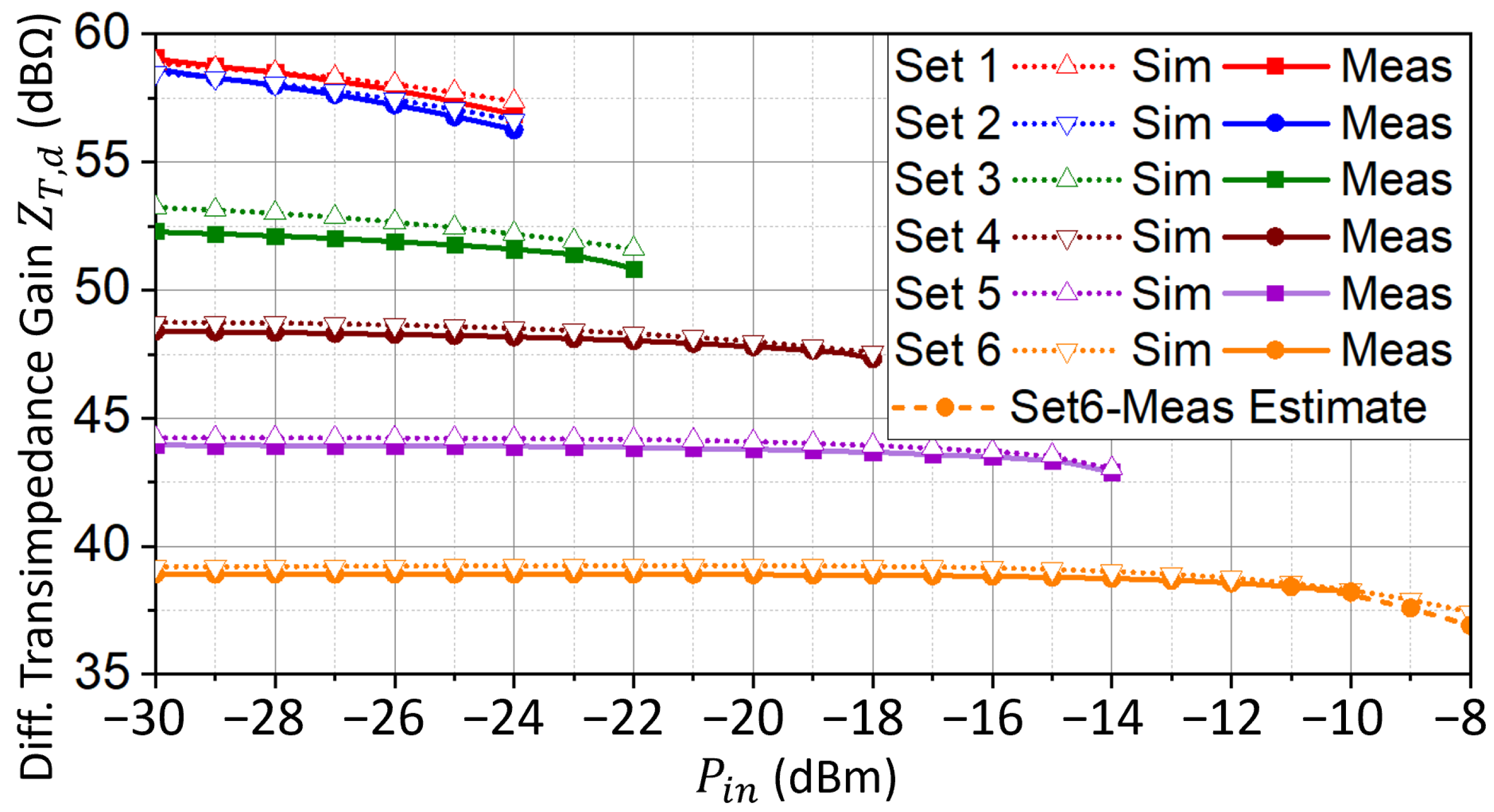
The input-referred 1 dB compression point (IP1dB) is shown in Figure 8 with input power swept at 100 MHz.
The IP1dB ranges from –26.75 to –9.75 dBm across settings 1–6, proving that the gain variation design also greatly increases the IP1dB. The results of the IP1dB are also in Table 2 below.
5.3. Noise and Dynamic Range
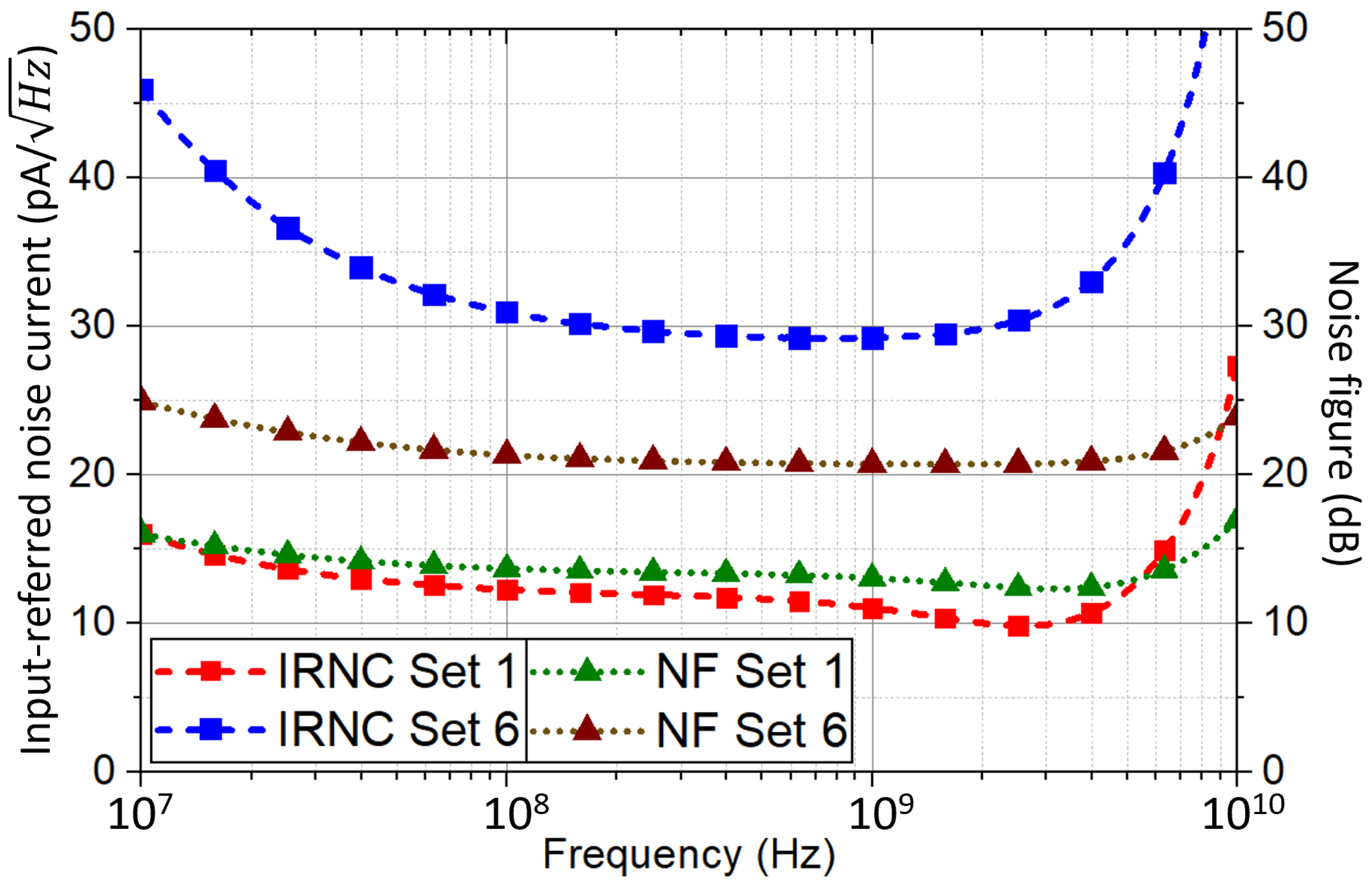
Both the input-referred noise current (IRNC) and noise figure (NF) of the TIA are simulated and plotted in Figure 9.
The IRNC and NF at 4 GHz for the maximum gain setting are 10.7 and 12.4 dB, respectively. The dynamic range lower limit is determined by IRNC at maximum gain and 4 GHz, as well as using a signal to noise ratio (SNR) of 49 for TIA specification [8]. This gives a minimum () of 33.2 µA. The dynamic range upper limit is determined by the IP1dB at minimum gain during high . Using gives a maximum of 1.46 mA. Thus, using the gain range as a parameter allows for both the IRNC and the IP1dB of the TIA design.
5.4. Eye Diagrams
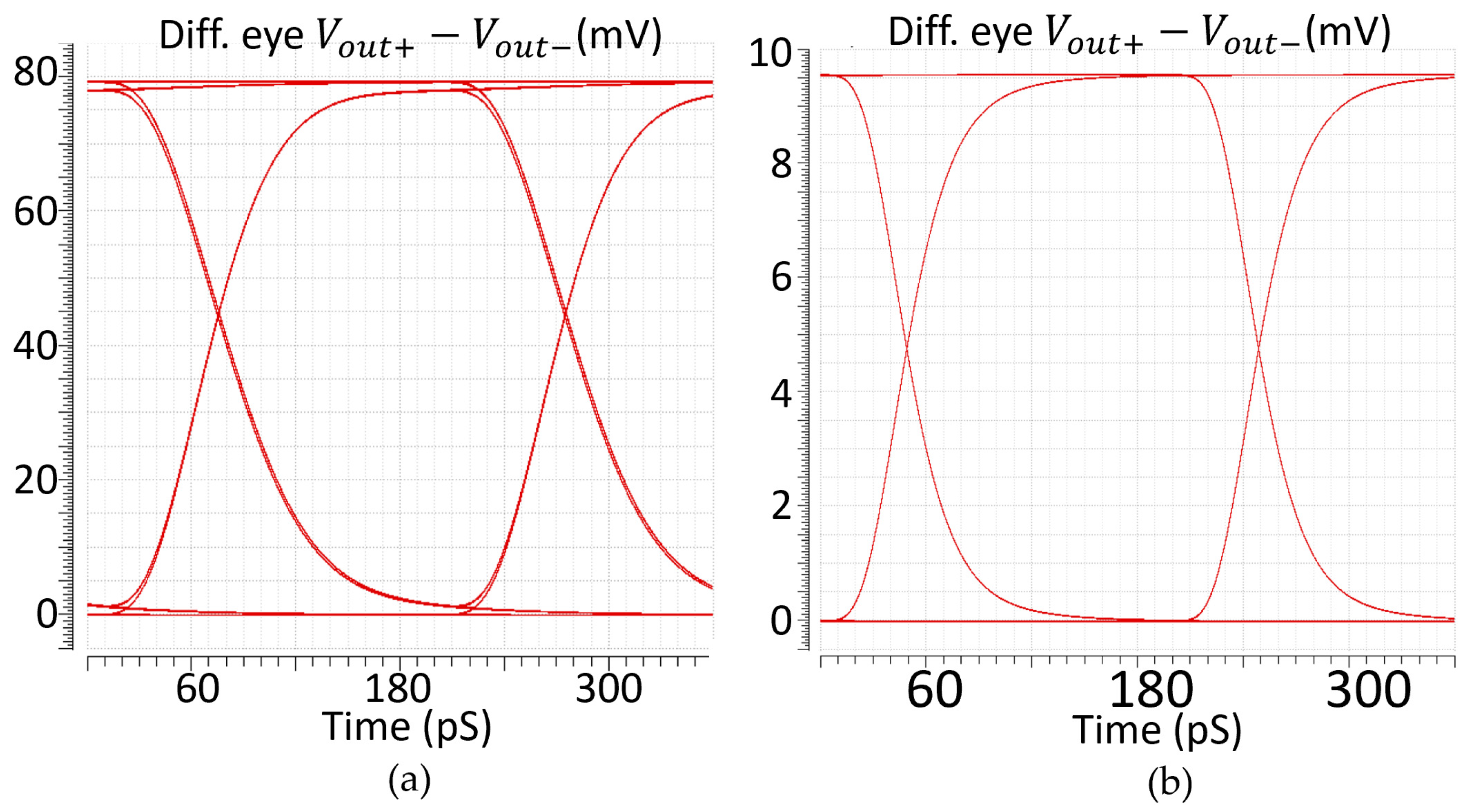
The simulated differential () eye diagrams of the TIA design are plotted in Figure 10 at the maximum and minimum gain settings with a 5 Gb/s 10 m pseudorandom binary sequence (PRBS) input. The PRBS signal is used to prove that the TIA is able to function for any type of sequence of programmed signal.
As shown in Figure 10, the eye openings at both settings are large and clear with little jitter, showing no distortion of the input signal throughout the TIA and thus suitable for VLC.
5.5. Load Capacitance Invariability
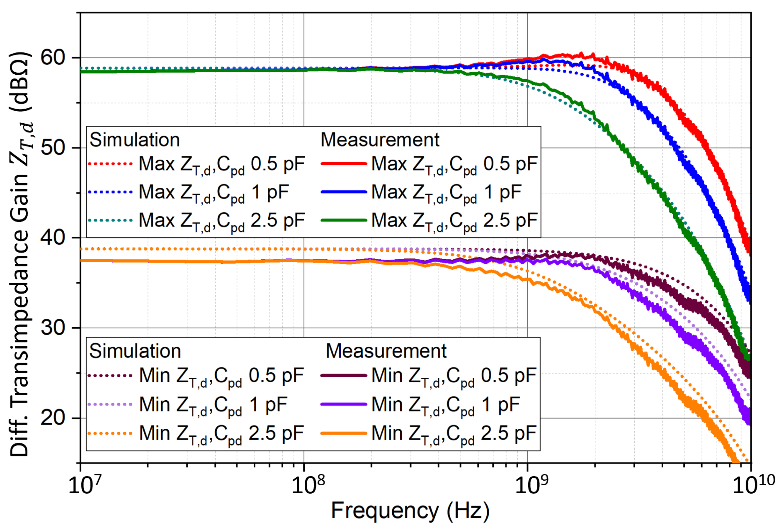
The S-parameter differential transimpedance gain measurement results can also be plotted with a range of larger values to prove its input load shielding and load capacitance invariance ability. The frequency response when the load is varied is shown in Figure 11.
As shown in Figure 11, when is increased from 0.5 pF to 2.5 pF (500%), the measured bandwidth drops from 4.15 GHz to 1.54 GHz, which is only a drop of 63% for the TIA maximum gain setting. Likewise, the bandwidth drops from 4.04 GHz to 1.24 GHz (drop 69%) for the minimum gain setting. The frequency response also does not peak when is increased, proving that it is also a more stable design, unlike [8]. A -invariance TIA design would allow a larger photodiode to be used to absorb more light signal and thus output a more detectable current to input into the TIA. Hence, this increases the range of distance between the transceiver and receiver.
6. Discussion and Comparison
A figure of merit (FOM) is used to compare the TIA designs [8]:
Table 3 compares this TIA design with other recent measured variable-gain TIAs and it has the highest FOM among all the designs.
The architecture of proposed TIA design in this paper is different and improved from the various compared designs. The designs in [13,15,16] only have either a CG, CS or inverter-type input stage, making it difficult to balance the gain-bandwidth trade-off. Conversely, the input stage of the proposed design has both CG and CS in a modified cross-coupled RGC design. This, together with the unique combined active inductor with capacitive degeneration structure in its mid-stage allows it to have a significantly larger bandwidth over [13,15,16], making it suitable for high frequency operation unlike those other designs.
Although the bandwidths of the designs in [8] are larger, their power consumption are much larger due to the multiple CS stages required to increase the gain. The designs in [8] also lack a current mirror current source and thus result in a risk of transistors being biased out of their ideal operating regions, reducing the actual input signal dynamic range. Thus, the TIA presented in this paper is the overall best design based on both its practicability for VLC applications and on the FOM used.
7. Conclusions
The authors present an inductorless variable-gain TIA using the UMC 40 nm CMOS process that has a unique single-to-differential cross-coupled modified RGC input stage and a modified -doubler mid-stage with a unique combined active inductor and capacitive degeneration design for bandwidth enhancement. The measured transimpedance gain range of 37.5–58.7 dBΩ and bandwidth of 4.15 GHz show that the TIA is suitable for practical high-speed visible light communication applications.
Author Contributions
S.B.S.L. contributed to the entire design process, including the circuit schematic, layout, simulation results in software and measurement results of the actual chip of the circuit, as well as the writing of this paper. K.S.Y. is the overall project Principal Investigator. All authors have read and agreed to the published version of the manuscript.
Funding
This research received no external funding.
Acknowledgments
The authors would like to acknowledge the Singapore University of Technology and Design (SUTD) for their support of this research and United Microelectronics Corporation (UMC) for the process design kit.
Conflicts of Interest
The authors declare no conflict of interest.
References
- Karunatilaka, D.; Zafar, F.; Kalavally, V.; Parthiban, R. LED Based Indoor Visible Light Communications: State of the Art. IEEE Commun. Surv. Tutorials 2015, 17, 1649–1678. [Google Scholar] [CrossRef]
- Zhang, Y.; Wang, L.; Wang, K.; Wong, K.S.; Wu, K. Recent Advances in the Hardware of Visible Light Communication. IEEE Access 2019, 7, 91093–91104. [Google Scholar] [CrossRef]
- Romanova, A.; Barzdenas, V. A Review of Modern CMOS Transimpedance Amplifiers for OTDR Applications. Electronics 2019, 8, 1073. [Google Scholar] [CrossRef] [Green Version]
- Säckinger, E. Analysis and Design of Transimpedance Amplifiers for Optical Receivers; Wiley: Hoboken, NJ, USA, 2017. [Google Scholar] [CrossRef]
- Razavi, B. Design of Integrated Circuits for Optical Communications; John Wiley & Sons, Inc.: Hoboken, NJ, USA, 2003. [Google Scholar]
- Lee, S.B.S.; Liu, H.; Yeo, K.S. An inductorless 6-GHz variable gain differential transimpedance amplifier in 0.18-μm SiGe BiCMOS. In Proceedings of the IEEE International Symposium on Circuits and Systems (ISCAS), Sapporo, Japan, 26–29 May 2019. [Google Scholar]
- Lee, S.B.S.; Liu, H.; Yu, X.; Chen, J.-M.; Yeo, K.S. An Inductorless 5-GHz Differential Dual Regulated Cross-Cascode Transimpedance Amplifier using 40 nm CMOS. In Proceedings of the 2019 IEEE 13th International Conference on ASIC (ASICON), Chongqing, China, 29 October–1 November 2019; pp. 1–4. [Google Scholar] [CrossRef]
- Lee, S.B.S.; Liu, H.; Yeo, K.S.; Yu, X.P. Design of differential variable-gain transimpedance amplifier in 0.18-µm SiGe BiCMOS. Electron. J. 2020, 9, 1058. [Google Scholar] [CrossRef]
- Park, S.M.; Yoo, H.-J. 1.25-Gb/s Regulated Cascode CMOS Transimpedance Amplifier for Gigabit Ethernet Applications. IEEE J. Solid-State Circuits 2004, 39, 112–121. [Google Scholar] [CrossRef] [Green Version]
- Costanzo, R.; Bowers, S.M. A Current Reuse Regulated Cascode CMOS Transimpedance Amplifier With 11-GHz Bandwidth. IEEE Microw. Wirel. Components Lett. 2018, 28, 816–818. [Google Scholar] [CrossRef]
- Chen, D.; Yeo, K.S.; Shi, X.; Do, M.A.; Boon, C.C.; Lim, W.M. Cross-Coupled Current Conveyor Based CMOS Transimpedance Amplifier for Broadband Data Transmission. IEEE Trans. Very Large Scale Integr. Syst. 2013, 21, 1516–1525. [Google Scholar] [CrossRef]
- Royo, G.; Sanchez-Azqueta, C.; Aldea, C.; Celma, S.; Gimeno, C. CMOS transimpedance amplifier with controllable gain for RF overlay. In Proceedings of the 12th Conference on Ph.D. Research in Microelectronics and Electronics (PRIME), Lisbon, Portugal, 27–30 June 2016; pp. 1–4. [Google Scholar] [CrossRef]
- Chen, R.Y.; Yang, Z.-Y. CMOS Transimpedance Amplifier for Gigabit-per-Second Optical Wireless Communications. IEEE Trans. Circuits Syst. II Express Briefs 2015, 63, 418–422. [Google Scholar] [CrossRef]
- Taghavi, M.H.; Belostotski, L.; Haslett, J.W.; Ahmadi, P. 10-Gb/s 0.13µm CMOS inductorless modified-RGC transimpedance amplifier. IEEE Trans. Circuits Syst. Regul. Pap. 2015, 62, 1971–1980. [Google Scholar] [CrossRef]
- Ngo, T.-H.; Kim, C.-H.; Kwon, Y.J.; Ko, J.S.; Kim, D.-B.; Park, H.-H. Wideband Receiver for a Three-Dimensional Ranging LADAR System. IEEE Trans. Circuits Syst. I Regul. Pap. 2012, 60, 448–456. [Google Scholar] [CrossRef]
- Royo, G.; Martinez-Perez, A.D.; Sanchez-Azqueta, C.; Aldea, C.; Celma, S. A Highly Linear Low-Noise Transimpedance Amplifier for Indoor Fiber-Wireless Remote Antenna Units. Electronics 2019, 8, 437. [Google Scholar] [CrossRef] [Green Version]
Figure 1.
Architecture of the transmitter and receiver modules of the VLC system.

Figure 2.
(a) Schematic and (b) simplified loop diagram of the proposed TIA single-to-differential input stage.
Figure 2.
(a) Schematic and (b) simplified loop diagram of the proposed TIA single-to-differential input stage.

Figure 3.
Schematic of the modified -doubler mid-stage of the proposed TIA.

Figure 4.
(a) Transistor-level schematic of the CMFB circuit and (b) buffer stage.

Figure 5.
Layout of the TIA input, mid and buffer stages.

Figure 6.
Die microphotographs of different magnifications of the TIA.

Figure 7.
Simulated and measured differential transimpedance gain of the TIA at different gain settings.
Figure 7.
Simulated and measured differential transimpedance gain of the TIA at different gain settings.

Figure 8.
Simulated and measured IP1dB of the TIA at different gain settings.

Figure 9.
Simulated IRNC and NF of the TIA at maximum and minimum gain settings.

Figure 10.
Simulated eye diagrams with 5 Gb/s 10 m PRBS input signal at (a) maximum and (b) minimum gain settings.
Figure 10.
Simulated eye diagrams with 5 Gb/s 10 m PRBS input signal at (a) maximum and (b) minimum gain settings.

Figure 11.
Simulated and measured transimpedance gain of the TIA with range of values.


Table 1.
Bias settings for all DC pads for the TIA design and for the various gain and peaking settings.
Table 1.
Bias settings for all DC pads for the TIA design and for the various gain and peaking settings.
| Bias Settings for All DC Pads | ||||||
|---|---|---|---|---|---|---|
| Pad | DC (V) | Pad | DC (V) | Pad * | DC (V) | I (mA) |
| 1 | 1.6 | 0.7 | 1.4 | |||
| 0.85 | 1 | 0.9 | 2.9 # | |||
| 0.2 | 1 | 1 | 0.12 | |||
| Variable-gain and peaking DC biasings for different settings | ||||||
| TIA gain setting | (V) | (V) | (V) | (V) | ||
| 1 (highest gain) | 1 | 1 | 1 | 1 | ||
| 2 | 1.4 | 1.2 | 1 | 1 | ||
| 3 | 1.6 | 1.4 | 1 | 1 | ||
| 4 | 1.7 | 1.5 | 1 | 1.4 | ||
| 5 | 1.8 | 1.5 | 1.4 | 1.5 | ||
| 6 (lowest gain) | 1.9 | 1.5 | 1.7 | 1.6 | ||
* , are voltage-biased for equivalent biases. # have separate current mirror biasings, hence .
Table 2.
Simulated and measured gain, bandwidth and IP1dB of the TIA.
| TIA Gain Setting | Sim | Sim BW (GHz) | Meas | Meas BW (GHz) | Sim IP1dB (dBm) | Meas IP1dB (dBm) |
|---|---|---|---|---|---|---|
| 1 (highest gain) | 58.9 | 4.17 | 58.7 | 4.15 | −25.25 | −26.75 |
| 2 | 58.6 | 3.96 | 57.5 | 4.35 | −25.75 | −27 |
| 3 | 53.1 | 5.38 | 52.4 | 5.07 | −24 | −23.25 |
| 4 | 48.5 | 5.63 | 48.0 | 4.77 | −18.75 | −18.25 |
| 5 | 44.1 | 5.00 | 43.7 | 4.35 | −14.25 | −14 |
| 6 (lowest gain) | 38.8 | 4.23 | 37.5 | 4.04 | −9.75 | −9.75 * |
* Note that measured IP1dB for set 6 is extrapolated as the measured range is not wide enough; the shape of the measured curve is similar to the simulated curve.
Table 3.
Table of comparison of this TIA design with other recent works.
| Parameter | [8] a | [13] | [15] b | [16] | This Work | |
|---|---|---|---|---|---|---|
| Technology | 0.18 µm CMOS | 0.18 µm CMOS | 0.13 µm CMOS | 65 nm CMOS | 40 nm CMOS | |
| (V) | 1.8 | 1.8 | 3 | 1.2 | 1.6 | |
| (pF) | 0.25 | 0.5 | 2 | 0.45 | 0.5 | |
| Max gain (dBΩ) | 60.6 | 62.8 | 69.3 | 78 | 76 | 58.7 |
| Gain range (dBΩ) | 36.1 | 35 | 13.5 | 30 | 16 | 21.2 |
| BW (GHz) | 6.42 | 5.22 | 1 | 0.64 | 0.3 | 4.15 |
| Power (mW) | 30.7 | 27.5 | 6 | 114 | 6 | 7.84 |
| Area (mm2) | 0.0085 | 0.0085 | 0.0075 | 0.587 | 0.015 | 0.001 |
| 10.3 c | 21.7 c | 9.33 | 5.6 | 2 c | 10.7 c | |
| FOM | 2022 | 2293 | 3282 | 2676 | 2271 | 4831 |
a This paper has two different designs, b for the entire receiver module including TIA, c simulated data.
Publisher’s Note: MDPI stays neutral with regard to jurisdictional claims in published maps and institutional affiliations. |
© 2021 by the authors. Licensee MDPI, Basel, Switzerland. This article is an open access article distributed under the terms and conditions of the Creative Commons Attribution (CC BY) license (https://creativecommons.org/licenses/by/4.0/).
Share and Cite
MDPI and ACS Style
Lee, S.B.S.; Yeo, K.S. A 4 GHz Single-to-Differential Cross-Coupled Variable-Gain Transimpedance Amplifier for Optical Communication. Electronics 2021, 10, 3042. https://0-doi-org.brum.beds.ac.uk/10.3390/electronics10233042
AMA Style
Lee SBS, Yeo KS. A 4 GHz Single-to-Differential Cross-Coupled Variable-Gain Transimpedance Amplifier for Optical Communication. Electronics. 2021; 10(23):3042. https://0-doi-org.brum.beds.ac.uk/10.3390/electronics10233042
Chicago/Turabian StyleLee, Samuel B. S., and Kiat Seng Yeo. 2021. "A 4 GHz Single-to-Differential Cross-Coupled Variable-Gain Transimpedance Amplifier for Optical Communication" Electronics 10, no. 23: 3042. https://0-doi-org.brum.beds.ac.uk/10.3390/electronics10233042
Note that from the first issue of 2016, this journal uses article numbers instead of page numbers. See further details here.