Article

Study of Thermal Stress Fluctuations at the Die-Attach Solder Interface Using the Finite Element Method

School of Materials Science and Engineering, University of Science and Technology Beijing, Beijing 100083, China
*
Author to whom correspondence should be addressed.
These authors contributed equally to this work and should be considered as first co-authors.
Submission received: 19 November 2021 / Revised: 20 December 2021 / Accepted: 20 December 2021 / Published: 25 December 2021
(This article belongs to the Special Issue Thermal Management of Electronic Packaging)

Abstract

:
Solder joints in electronic packages are frequently exposed to thermal cycling in both real-life applications and accelerated thermal cycling tests. Cyclic temperature leads the solder joints to be subjected to cyclic mechanical loading and often accelerates the cracking failure of the solder joints. The cause of stress generated in thermal cycling is usually attributed to the coefficients of thermal expansion (CTE) mismatch of the assembly materials. In a die-attach structure consisting of multiple layers of materials, the effect of their CTE mismatch on the thermal stress at a critical location can be very complex. In this study, we investigated the influence of different materials in a die-attach structure on the stress at the chip–solder interface with the finite element method. The die-attach structure included a SiC chip, a SAC solder layer and a DBC substrate. Three models covering different modeling scopes (i.e., model I, chip–solder layer; model II, chip–solder layer and copper layer; and model III, chip–solder layer and DBC substrate) were developed. The 25–150 °C cyclic temperature loading was applied to the die-attach structure, and the change of stress at the chip–solder interface was calculated. The results of model I showed that the chip–solder CTE mismatch, as the only stress source, led to a periodic and monotonic stress change in the temperature cycling. Compared to the stress curve of model I, an extra stress recovery peak appeared in both model II and model III during the ramp-up of temperature. It was demonstrated that the CTE mismatch between the solder and copper layer (or DBC substrate) not only affected the maximum stress at the chip–solder interface, but also caused the stress recovery peak. Thus, the combined effect of assembly materials in the die-attach structure should be considered when exploring the joint thermal stresses.

1. Introduction

With the development of semiconductor technologies, SiC, GaN and other third-generation semiconductor materials with wide band-gap characteristics are widely used in power modules [1]. The SiC chip is generally attached to the circuit board through a solder layer (i.e., die-attach structure), which provides mechanical support and heat dissipation protection for the chip [2,3]. As power modules often work under high-current, high-power density and high-temperature conditions, higher demands are placed on the die-attach technology to ensure the reliability of the power modules [4,5,6].
In order to meet the requirements of die-attach technologies and the Restriction of Hazardous Substances (RoHS) directive, a series of die-attach materials, such as Sn–Ag, Sn–Ag–Cu (i.e., SAC) solder alloys and sintering silver paste were developed [7,8,9]. Among them, the SAC solder has become a type of widely used lead-free solder in the electronics industry by the virtue of its adequate thermal fatigue properties, strength, and wettability [10]. A firm joint is usually formed by the good metallurgical bond between the solder and the components being joined. However, in the practical application of various related devices, cracking failures of the die-attach structure can often be found [11]. Among them, cracking failures caused by temperature fatigue account for about 55% of die-attach structure failure [12]. Cracks are usually located at the chip–solder interface. For instance, Song et al. performed an accelerated temperature cycling (ATC) test of printed circuit board (PCB) test assemblies (which used five kinds of solders (SAC305, SAC387, SACC, SACS and SCN), respectively) and found that all the PCBs cracked after 4000 cycles of ATC tests. In addition, all the cracks were observed at the chip–solder interface [13]. Therefore, clarifying the causes of cracking during temperature cycling is of great value to power module reliability.
Through temperature cycling tests, it was found that due to the different coefficients of thermal expansion (CTE) between the chip and solder, thermal stress is generated and concentrated at the chip–solder interface during the temperature cycling process [14]. Excessive thermal stress can lead to cracking, which is the main cause of cracking failures [15,16]. By making the solder CTE closer to that of the chip, the thermal stress during thermal cycling can be reduced. However, literature reports show that even materials not directly bonded to the chip or solder may indirectly affect the thermal stress at the chip–solder interface. For instance, Chen et al. added a tungsten film (100 μm thick) to the solder layer in the die-attach structure, and they found that the tungsten film can effectively improve the stress distribution in the solder layer and reduce the shear stress at the chip–solder interface during thermal cycling simulations [17]. Therefore, an accurate analysis of the thermal stress at the chip–solder interface is important to understand its cracking failure behavior.
Usually, it is quite difficult to directly observe the stress changes during temperature cycling by experimental methods. With the development of computer simulation technology, the finite element method (FEM) is widely used as an effective tool in the simulation analysis of stress, strain, and plastic work [18,19]. However, due to differences in model boundary condition and modeling scope, different phenomena can often be observed from thermal stress simulation results. For example, when Otiaba et al. performed a thermal mechanical coupling analysis on a three-layer structure consisting of a chip, solder, and copper substrate (with constraints placed on the top of the chip), they found that the stresses in the solder joints varied monotonically with temperature loading in a periodic manner [3]. While Xie et al. performed a similar simulation (with constraints placed on the bottom of the copper layer), a small stress recovery peak was observed during the heating up stage [20]. Similar stress recovery phenomena can often be seen in temperature cycling simulations, but there is no clear explanation for their formation mechanism and the reasonability [21,22].
In this study, three models which include different assembly materials were built based on a die-attach structure consisting of a SiC chip, a solder layer, and a direct bonded copper (DBC) substrate. Thermal cycling simulations were performed for the three models with the FEM. By analyzing the deformation and stress distribution in the solder layer and the stress change at the chip–solder interface, the effects of the boundary conditions and the modeling scope on the chip–solder interfacial thermal stress were studied. The aim of this work is to investigate the effect of non-directly bonded materials on specific interfacial stress, and the causes of stress recovery peak in temperature cycling simulations.

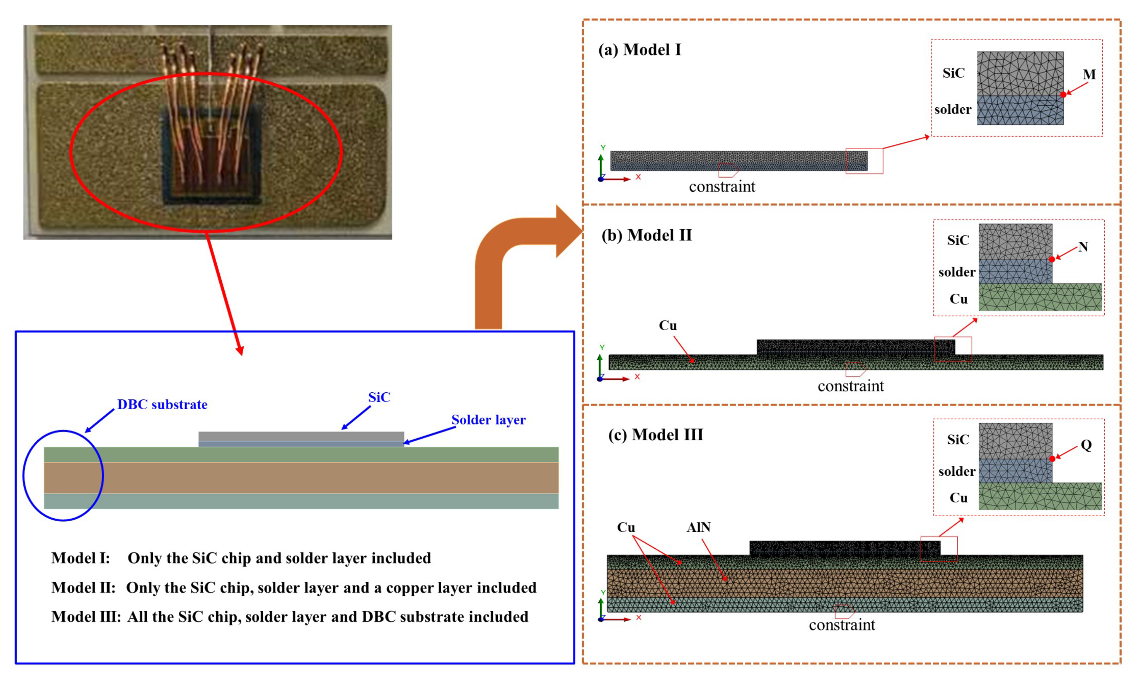
2. Finite Element Modeling

2.1. Finite Element Model Structure

A simplified die-attach structure in typical power modules was employed (Figure 1). It consisted of a SiC chip, a solder layer, and a DBC substrate. To investigate the effect of different modeling scopes on the simulation results, three different two-dimensional models were established with the ANSYS software: model I, a model containing only the chip and the solder layer; model II, a model containing the chip, the solder layer, and the copper layer; and model III, a model containing the chip, the solder layer, and the DBC substrate. Among them, the SiC chip size was 4.00 mm × 0.18 mm, the solder layer size was 4.00 mm × 0.12 mm, the copper layer size was 10.00 mm × 0.30 mm, and the AlN ceramic layer size was 10.00 mm × 0.60 mm. Since the focus was on exploring the effect of CTE mismatch on thermal stress, these materials were ideally interconnected assuming no defects and without considering interfacial reactions. The joint strength was also ignored. The model was meshed using Plane183 elements with 8 nodes, and the mesh elements were triangular elements. The chip–solder interface was locally refined to ensure the accuracy of stress calculation result at the target location (the points M, N and Q in Figure 1, at the corner of the chip–solder interface near the solder side). The mesh for model I consists of 5359 nodes and 2536 elements, model II consists of 11,155 nodes and 5334 elements, model III consists of 15,014 nodes and 7265 elements.

2.2. Material Properties

The lead-free SAC405 solder alloy contains 95.5% tin (Sn), 4.0% silver (Ag) and 0.5% copper (Cu) and is usually described as Sn95.5Ag4.0Cu0.5. It is considered one of the commonly used lead-free solder alloys because of its environmental compatibility and service reliability [23]. AlN ceramic has comprehensive advantages, such as high thermal conductivity, close CTE to Si, good mechanical properties, etc. [24]. As a typical product of AlN ceramic, the AlN-DBC substrate has a high current carrying capacity and plays an important role in power modules. The material parameters used in this study were derived from experimentally measured values reported in the literature (Table 1) [25,26].
Both the SiC chip and AlN ceramic substrate were considered isotropic linear elastic materials. Usually, the solder is described by a unified viscoplastic model or creep model [27,28]. However, the results calculated using these constitutive models are after creep and do not reflect the state of the material before and during creep. In this study, the multilinear kinematic hardening model was used to describe the stress–strain condition in the initial state without creep. The stress–strain curves of SAC405 solder in the elastic deformation stage and uniform plastic deformation stage at different temperatures were obtained from the literature [29].
The Chaboche nonlinear kinematic hardening model was utilized to describe the plastic deformation of copper layer (Table 2) [30]. The corresponding yield criterion was calculated as
F = 3 2 ( { s } { α } ) T [ M ] ( { s } { α } ) Y = 0
where {s} represents the deviatoric stress tensor, {α} is the back stress variable and Y denotes the yield stress. The back stress for the Chaboche constitutive model is shown below:
{ α } = i n { α } i
{ Δ α } i = 2 3 C i { Δ ε p l } γ i { α } i { Δ p } + 1 C i d C i d T Δ θ { α } i
where {∆εpl} is the plastic strain tensor, {∆p} is the accumulated plastic strain tensor, θ is the temperature, Ci and γi respectively represent the material constants of the Chaboche model, and n is the number of superimposed kinematic models in the back stress tensor.

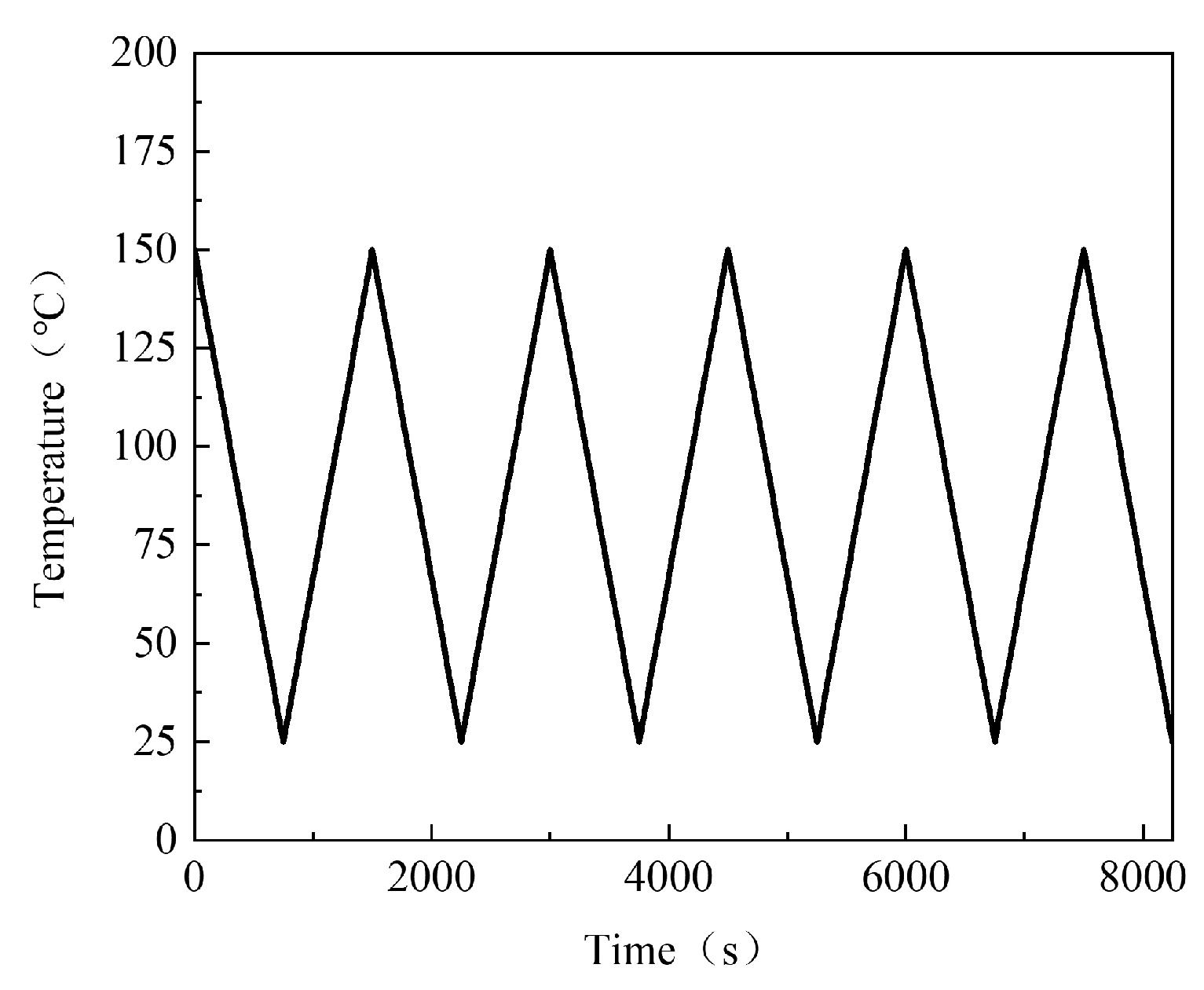
2.3. Load and Boundary Conditions

This study selected 150 °C as the temperature reference point (the structure was stress free) and applied the same homologous temperature load to the three models. As shown in Figure 2, the temperature loading was divided into 11 load steps: the first load step represented the model lowering from the preparation temperature to room temperature (25 °C), and the next 10 load steps represented 5 complete temperature cycles. The range of temperature cycles was 25–150 °C. Considering IEC test standard 60749-25, the temperature change rate was 10 °C/min [31].
To compare the effects of different boundary conditions on the die-attach structure, two boundary conditions were applied to each of the three models. Under the fixed constraint condition, the deformation of the constrained layer was limited (Equation (4)). Under the non-fixed constraint condition, the warpage was neglected and only the deformation of the constrained layer in the y-direction was restricted, while it remained free to deform in the x-direction (Equation (5)). The constraints were set at the bottom edge of the three models (Figure 1).
u ( y ) = u ( x ) = 0
u ( y ) = 0 ,   u ( x ) = free
where u(x) and u(y) represent the displacement in the x and y directions, respectively.

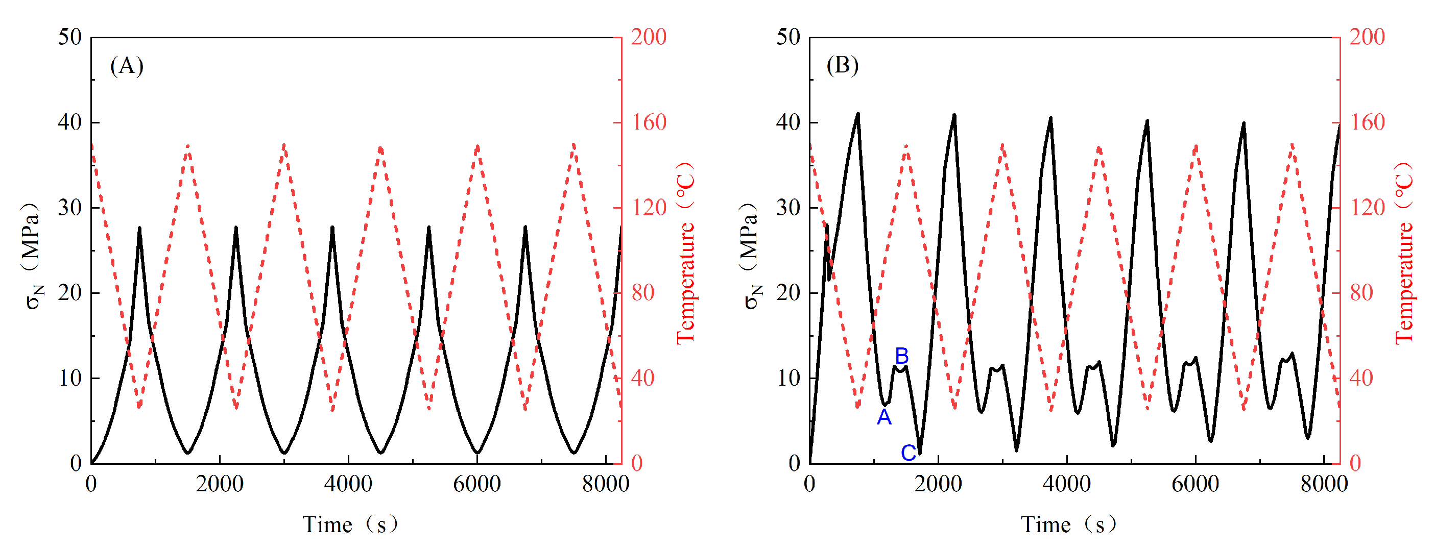
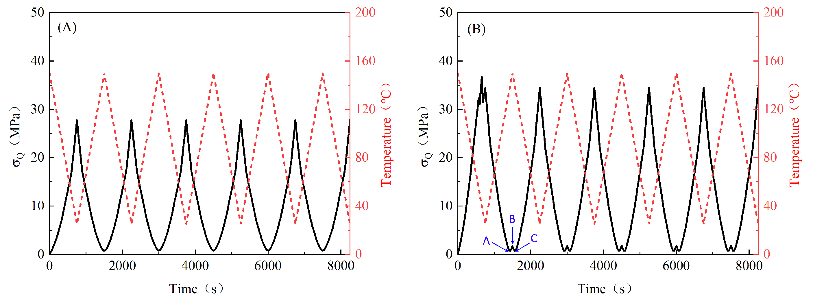
3. Results and Discussion

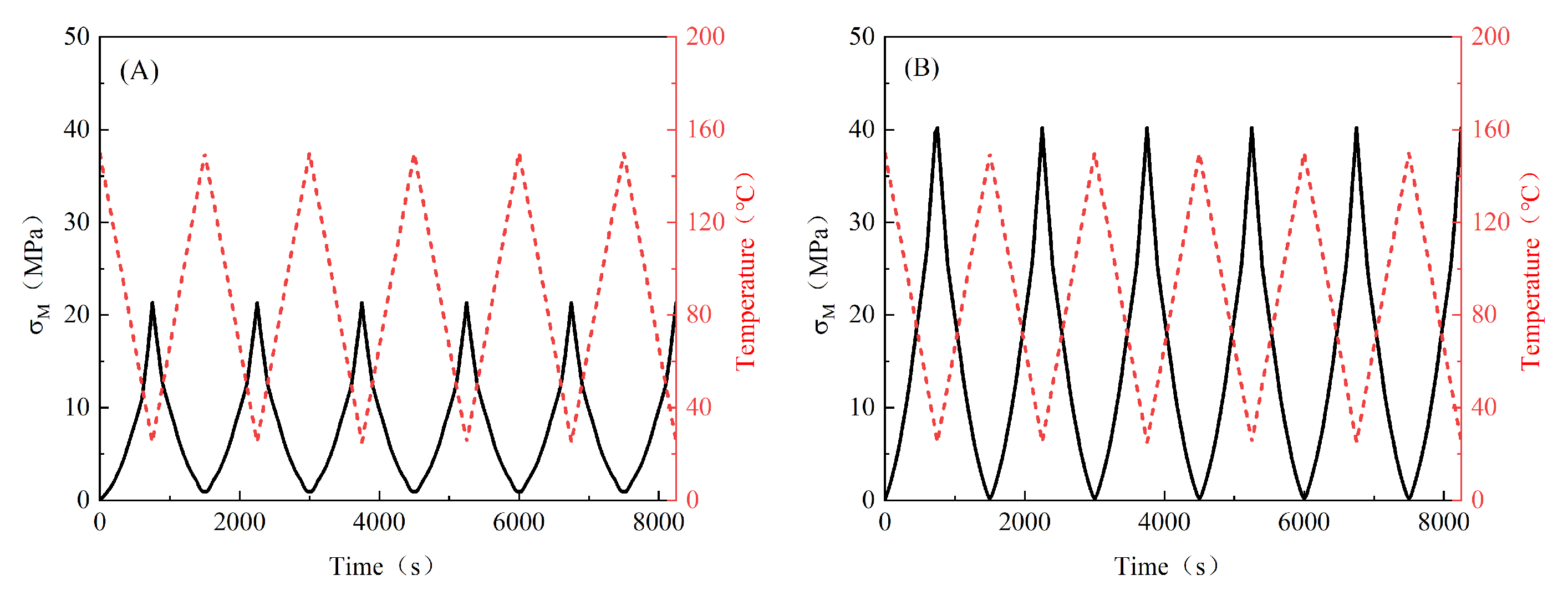
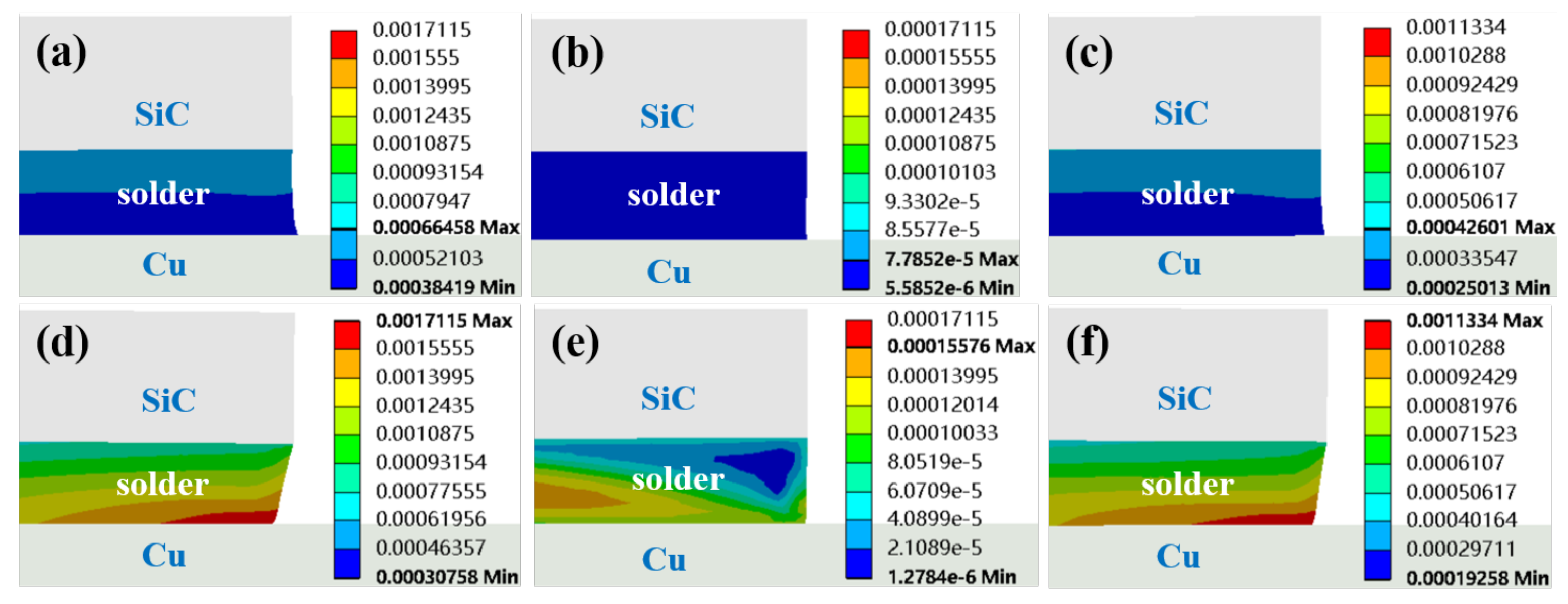
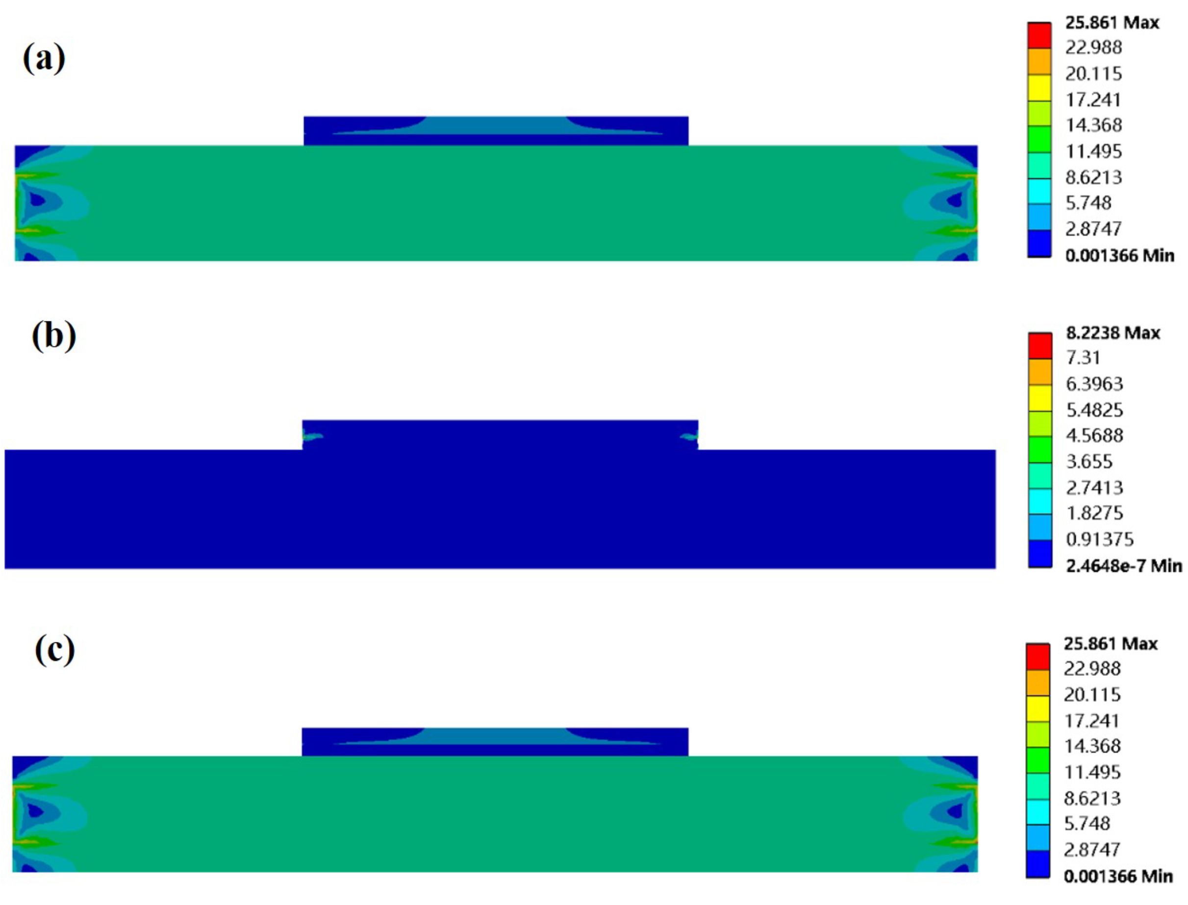
3.1. Effects of Boundary Conditions

For model I (Figure 1a) under the fixed constraint, the stress at point M (σM) varied periodically and monotonically with temperature loading (Figure 3A). The σM decreased when the temperature increased and increased when the temperature decreased. The maximum value of σM was about 21.3 MPa, which corresponded to the lowest temperature. The minimum value of σM was about 0.2 MPa, which corresponded to the maximum temperature. Under the non-fixed constraint condition, the σM also varied periodically and monotonically with the temperature loading (Figure 3B). The maximum and minimum values of σM also corresponded to the minimum and maximum temperatures. However, the maximum value of σM was obviously different, increasing from 21.3 MPa under fixed constraint to 40.2 MPa. It was clear that the only source of σM was the CTE mismatch between the chip and the solder layer. Since the CTE of SAC405 was significantly higher than SiC, the fixed constraint was equivalent to limiting the deformation of the solder layer. This equivalently reduced the degree of chip–solder CTE mismatch. Thus, the maximum value of σM obtained under fixed constraint was significantly smaller than under a non-fixed constraint.
When the thermal cycling simulation was finished, the deformation and stress contour plots of model I were intercepted. In the deformation contour plots, the edge of the solder layer obtained under the fixed constraint had a positive trapezoid shape, while the edge of the solder layer obtained under the non-fixed constraint had an inverted trapezoid shape (Figure 4a,c). Under the fixed or non-fixed constrain conditions, both the chip and solder layer should be in a shrinkage state from the initial stress-free state (150 °C) to the simulation end (25 °C) [32]. The solder layer apparently shrank more under the non-fixed constraint. However, the whole shrinkage of the solder layer was restrained under the fixed constraint. That is, the equivalent CTE of the solder was smaller than that of the solder under non-fixed constraint. The stress contour plots revealed that the maximum stress in the solder layer under fixed constraints located at the bottom side, while it transferred to the chip–solder interface corner under non-fixed constraints (Figure 4b,d). The above results confirmed that the constraints had a significant effect on the deformation and stress distribution of the solder layer, which must be the main factor for the difference in the maximum σM values under different constraints.

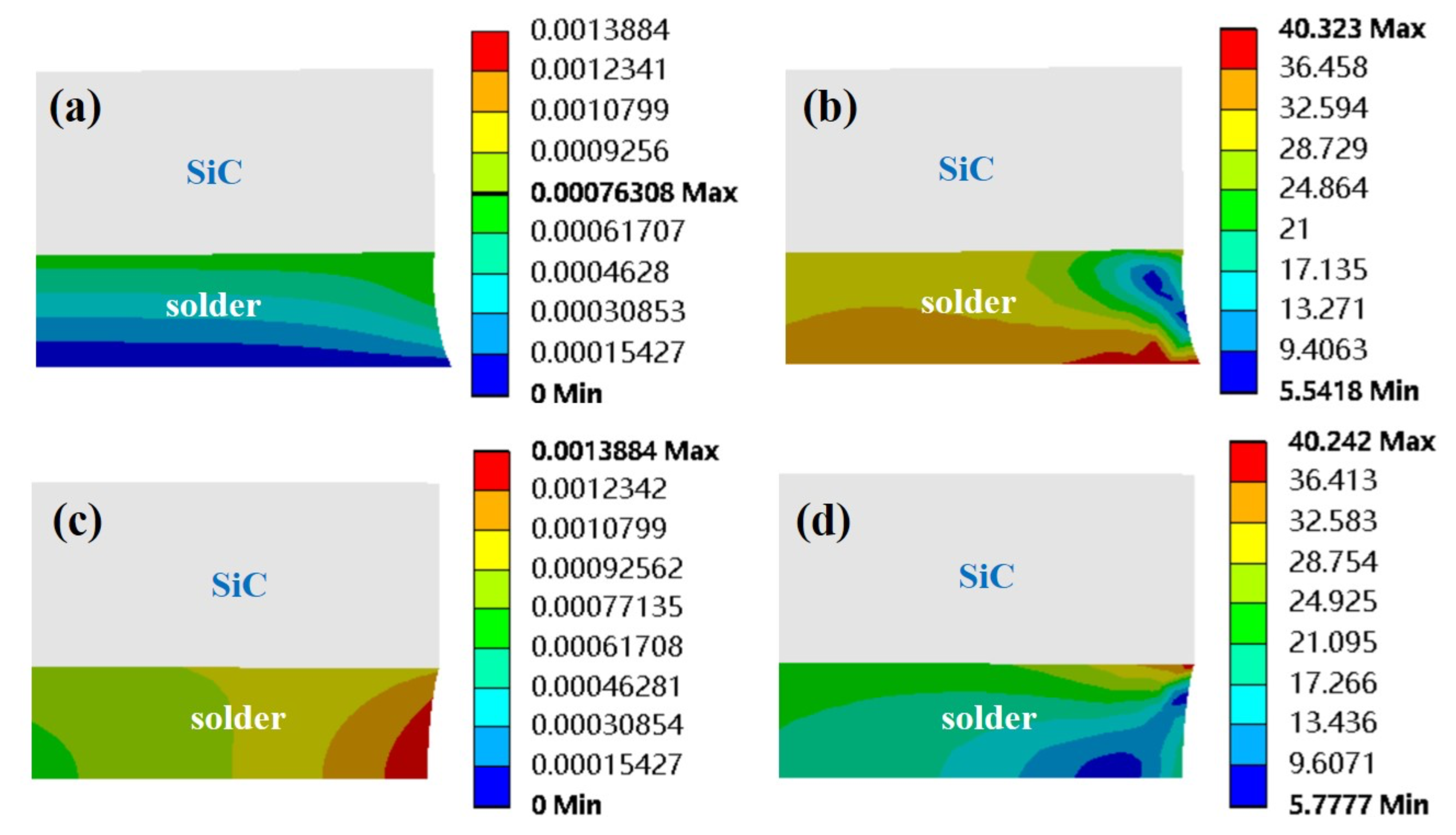
3.2. Effects of Modeling Scope

When model II (Figure 1b) was under a fixed constraint, the N-point stress (σN) still varied monotonically and cyclically with temperature loading (Figure 5A). In that condition, the equivalent CTE of the copper layer was quite small because of its limited deformation. Therefore, the main source of σN was still the CTE mismatch between the chip and the solder layer. Since the fixed copper layer would hinder the shrinkage of the solder layer, the equivalent CTE of the solder layer should be less than 26.0 ppm/K and larger than the value in model I under the fixed constraint. Thus, the actual ΔCTE value of the chip and solder layer in model II (under fixed constraint) was between the ΔCTE values of the fixed and non-fixed constraints in model I. As a result, the maximum σN was about 27.7 MPa (Figure 5A), which was between 20.3 MPa and 40.2 MPa, obtained for the fixed and non-fixed constraints in model I.
Under the non-fixed constraint condition, a distinct stress fluctuation (i.e., the stress recovery peak, about 11.7 MPa) can be observed at the location where σN should be at a minimum (Figure 5B). The stress fluctuation phenomenon was often observed in the thermal stress of joints in temperature cycling simulations. For instance, Zhang et al. evaluated the von Mises stress of different lead-free solder joints in a chip scale package device (consisting of the chip, solder joints and copper pad) under thermal cyclic loading. Distinct stress recovery peaks during the ramp-up of temperature could be observed in all the solder joints [21]. However, Amalu et al. performed a similar simulation, and no distinct stress fluctuations were found in the solder joint, while intermetallic compound layers were added at the up and bottom sides of the solder joints, respectively [31]. Although the stress fluctuation must be caused by the CTE mismatch of the assembly materials in the die-attach structure, the corresponding mechanism and possible impact on module reliability were not clarified.
For the deformation contour plots (Figure 6a–c) corresponding to the stress recovery peak (i.e., points A, B and C in Figure 5B), the internal deformation of solder layer was relatively uniform and slight under fixed constraint. But at the stress recovery peak location under the non-fixed constraint (Figure 6e), the shrinkages of the copper layer and the solder layer should have an interaction and it disturbed the normal deformation of solder layer. Therefore, the stress recovery peak should be attributed to the superposition of two stresses generated by the chip–solder layer CTE mismatch and the solder layer and copper layer CTE mismatch. In addition, probably due to this stress superposition effect, the maximum σN reached 41.1 MPa under the non-fixed constraint [33].

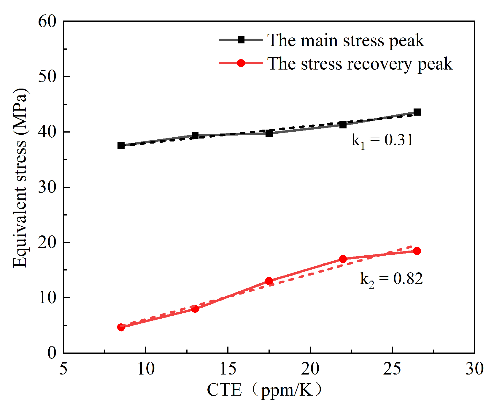
3.3. Effects of Substrates

The Q-point stress (σQ) under temperature cycling was simulated and analyzed using model III (Figure 1c). The DBC substrate consisted of an AlN ceramic layer and double-side copper layers, which were considered as an entirety. Its equivalent thermal expansion coefficient was calculated by the following equation [34]:
α D B C = α c e r a m i c + ( α C u α c e r a m i c ) · E C u · d C u E C u · d C u + E c e r a m i c · d c e r a m i c
where α represents the CTE value, E represents the modulus of elasticity, and d is the thickness of each layer. The equivalent CTE of the overall DBC substrate was about 6.5 ppm/K.
As shown in Figure 7, a stress recovery peak of σQ was observed under the non-fixed constraint condition, with no stress recovery peaks under the fixed constraint. Since the DBC substrate was considered as an entirety (which played a similar role and function as the copper layer in model II), the σQ varied in the same manner as σN under the temperature cycling. However, the stress recovery peak of σQ (1.7 ppm/K, Figure 7B) was significantly smaller than the corresponding stress recovery peak of σN (11.7 ppm/K, Figure 5B).
For the stress recovery peak in Figure 7B, the corresponding stress contour plots of model III are depicted in Figure 8. The corners of the copper and AlN layer interface within the DBC substrate generally had high stresses. When the temperature loading reached its maximum value, the stress at this location basically returned to its initial stress-free state. In contrast, σQ was always smaller. However, while the stress at the corner of the copper–AlN interface returned to the stress-free state, σQ was enhanced. Due to the bonding with the AlN layer, the deformation of the upper copper layer was constrained. Therefore, the CTE mismatch between the solder layer and the upper copper layer in model III was larger than the state in model II. In other words, the DBC substrate limited the deformation of the solder layer more strongly than the individual copper layer, and it could more significantly reduce the CTE mismatch between the chip and the solder layer [35,36]. This was evidenced by the fact that the maximum σQ value in model III (Figure 7B) was lower than the maximum σN value in model II (Figure 5B). This complex interaction also affected the magnitude of stress recovery peak in model III [33].
To further analyze the effect of different substrate types or specifications on the stress recovery peak, the model II was used for σN simulations. The copper layer in model II was assumed to be a substrate, just like the substrate was considered as an entirety in model III. Here, the CTE value of the copper was set virtually to 8.5–26.5 ppm/K for the purpose of simulating different types of substrates [37]. As shown in Figure 9, the stress intensity of both the main peak and stress recovery peak enhanced almost linearly with the increase in the substrate CTE values. The slope of the stress recovery peak (k2 = 0.82) was larger than that of the main peak (k1 = 0.31). Meanwhile, the minimum value deviation method was also applied to compare the sensitivity of the main peak and stress recovery peak to the substrate CTE values [31]. As listed in Table 3, when the substrate CTE increased from 8.5 ppm/K to 26.5 ppm/K, the maximum relative change of the main peak was 16.3% and the maximum relative change of the stress recovery peak was 302.2%. It can be seen that the stress recovery peak value was more sensitive to the change in substrate CTE. This also proved that the stress recovery peak was mainly caused by the CTE difference between the solder layer and the substrate.
Since the DBC substrate could indirectly affect the thermal stress at the chip–solder interface and led to the appearance of stress recovery peak, the potential influence of all assembly materials in the die-attach structure should be considered when conducting studies, such as module life prediction and reliability estimation [38]. Especially when the intermetallic compound layer or additional functional film layer are included in the finite element models, their influence on the thermal stress will be more complex [39,40]. Since this study used a simplified model and did not consider the joint strength, a more in-depth evaluation combining simulation and experiment is needed in future studies to understand the real effect of stress recovery peak on module reliability. It will be meaningful for the design and reliability evaluation of die-attach structures.

4. Conclusions

The finite element method was used to analyze the effects of boundary conditions and modeling scopes on the stress at the chip–solder layer interface during thermal cycling. A simplified power die-attach structure, consisting of a SiC chip, a solder layer and a DBC substrate, was built to explore the influences of boundary conditions and modeling scopes on the thermal stress at the chip–solder interface corner during thermal cycling. The results indicate that the boundary conditions directly affect the stress magnitude and stress distribution in the solder layer. In addition, materials such as the copper layer or DBC substrate, which are not directly bonded to the chip–solder interface, also indirectly affected the chip–solder interfacial stress. Due to the superposition of two stresses generated by the chip–solder layer CTE mismatch and the solder layer and DBC substrate CTE mismatch, stress recovery peaks appear at the chip–solder layer interface stress curve during the ramp-up in temperature. The magnitude of the stress recovery peak will increase with the degree of CTE mismatch between the solder layer and the DBC substrate.

Author Contributions

Conceptualization, K.G. and H.Y.; data curation, J.Y.; formal analysis, L.Y., Y.D., S.Z. and W.B.; funding acquisition, H.Y.; investigation, L.Y., J.Y. and W.B.; methodology, L.Y., H.Y. and Y.W.; software, J.Y.; supervision, K.G., H.Y. and Y.W.; visualization, L.Y. and J.Y.; writing—original draft, J.Y.; writing—review and editing, L.Y. All authors have read and agreed to the published version of the manuscript.

Funding

This study was funded by the Guangdong Major Project of Basic and Applied Basic Research (2019B030302011) and the National Key Research and Development Program of China (2016YFB0700201).

Conflicts of Interest

The authors declare no conflict of interest.

References

  1. Ballestín-Fuertes, J.; Muñoz-Cruzado-alba, J.; Sanz-Osorio, J.F.; Laporta-Puyal, E. Role of wide bandgap materials in power electronics for smart grids applications. Electronics 2021, 10, 677. [Google Scholar] [CrossRef]
  2. Jiang, C.; Guo, W.; Fan, J.; Qian, C.; Fan, X.; Zhang, G. Optimization of reflow soldering process for white LED chip-scale-packages on substrate. In Proceedings of the International Conference on Electronic Packaging Technology, Harbin, China, 16–19 August 2017; pp. 1309–1313. [Google Scholar]
  3. Otiaba, K.C.; Bhatti, R.S.; Ekere, N.N.; Mallik, S. Finite element analysis of the effect of silver content for Sn-Ag-Cu alloy compositions on thermal cycling reliability of solder die attach. Eng. Fail. Anal. 2013, 28, 192–207. [Google Scholar] [CrossRef]
  4. Barbagallo, C.; Rizzo, S.A.; Scelba, G.; Scarcella, G.; Cacciato, M. On the lifetime estimation of SiC power MOSFETs for motor drive applications. Electronics 2021, 10, 324. [Google Scholar] [CrossRef]
  5. Alves, L.F.S.; Lefranc, P.; Jeannin, P.-O.; Sarrazin, B.; Crebier, J.-C. Analysis of the multi-steps package (MSP) for series-connected SiC-MOSFETs. Electronics 2020, 9, 1341. [Google Scholar] [CrossRef]
  6. Fan, J.; Hu, A.; Pecht, M.; Chen, W.; Fan, X.; Xu, D.; Zhang, G. Fatigue damage assessment of LED chip scale packages with finite element simulation. In Proceedings of the International Conference on Electronic Packaging Technology, Shanghai, China, 8–11 August 2018; pp. 1642–1648. [Google Scholar]
  7. Mokhtar, N.Z.M.; Salleh, M.A.A.M.; Sandu, A.V.; Ramli, M.M.; Chaiprapa, J.; Vizureanu, P.; Ramli, M.I.I. Effect of electromigration and thermal ageing on the Tin whiskers’ formation in thin Sn–0.7Cu–0.05Ga lead (Pb)-free solder joints. Coatings 2021, 11, 935. [Google Scholar] [CrossRef]
  8. Yamamoto, M.; Shohji, I.; Kobayashi, T.; Mitsui, K.; Watanabe, H. Effect of small amount of Ni addition on microstructure and fatigue properties of Sn-Sb-Ag lead-free solder. Materials 2021, 14, 3799. [Google Scholar] [CrossRef] [PubMed]
  9. Yang, D.; Huang, Y.; Tian, Y. Microstructure of Ag nano paste joint and its influence on reliability. Crystals 2021, 11, 1537. [Google Scholar] [CrossRef]
  10. Huang, C.M.; Raj, A.; Osterman, M.; Pecht, M. Assembly options and challenges for electronic products with lead-free exemption. IEEE Access 2020, 8, 134194–134208. [Google Scholar] [CrossRef]
  11. Kang, M.S.; Kim, D.S.; Shin, Y.E. The effect of epoxy polymer addition in Sn-Ag-Cu and Sn-Bi solder joints. Materials 2019, 16, 960. [Google Scholar] [CrossRef] [PubMed] [Green Version]
  12. Depiver, J.A.; Mallik, S.; Amalu, E.H. Thermal fatigue life of ball grid array (BGA) solder joints made from different alloy compositions. Eng. Fail. Anal. 2021, 125, 105447. [Google Scholar] [CrossRef]
  13. Song, F.; Lo, J.C.; Lam, J.K.; Jiang, T.; Lee, S. A comprehensive parallel study on the board level reliability of SAC, SACX and SCN solders. In Proceedings of the Electronic Components and Technology Conference, Lake Buena Vista, FL, USA, 27–30 May 2008; pp. 146–154. [Google Scholar]
  14. Chen, Y.L.; Jia, J.Y.; Fu, H.Z.; Zhi, Z. Analysis of the BGA solder Sn-3.0Ag-0.5Cu crack interface and a prediction of the fatigue life under tensile stress. Int. J. Fatigue 2016, 87, 216–224. [Google Scholar] [CrossRef]
  15. Huang, X.G.; Han, Z.Y. Interface singular field analysis and thermal fatigue failure of solder joint in a stacked electronic modules. J. Mater. Sci. Mater. Electron. 2016, 27, 8299–8311. [Google Scholar] [CrossRef]
  16. ZHan, Y.; Huang, X.G. GA-BP in thermal fatigue failure prediction of microelectronic chips. Electronics 2019, 8, 542. [Google Scholar]
  17. Chen, C.; Choe, C.; Zhang, Z.; Kim, D. Low-stress design of bonding structure and its thermal shock performance (−50 to 250 °C) in SiC/DBC power die-attached modules. J. Mater. Sci. Mater. Electron. 2018, 29, 14335–14346. [Google Scholar] [CrossRef]
  18. ZYang, T.; Peng, B.; Gao, L. Research on the thermal fatigue life of CQFN packaging. In Proceedings of the International Conference on Electronic Packaging Technology, Shanghai, China, 8–11 August 2018; pp. 662–666. [Google Scholar]
  19. Psota, B.; Szendiuch, I. Modeling of microelectronic structures and packages using ANSYS software. In Proceedings of the International Spring Seminar on Electronics Technology, Tratanska Lomnica, Slovakia, 11–15 May 2011; pp. 354–357. [Google Scholar]
  20. Xie, X.; Bi, X.; Li, G. Thermal-mechanical fatigue reliability of PbSnAg solder layer of die attachment for power electronic devices. In Proceedings of the International Conference on Electronic Packaging Technology & High Density Packaging, Beijing, China, 10–13 August 2009; pp. 1181–1185. [Google Scholar]
  21. Zhang, L.; Han, J.; He, C.; Guo, Y. Reliability behavior of lead-free solder joints in electronic components. J. Mater. Sci. Mater. Electron. 2013, 24, 172–190. [Google Scholar] [CrossRef]
  22. Xu, Y.; Wang, L.; Wu, F.; Xia, W.; Liu, H. Effect of interface structure on fatigue life under thermal cycle with SAC305 solder joints. In Proceedings of the International Conference on Electronic Packaging Technology, Dalian, China, 11–14 August 2013; pp. 959–964. [Google Scholar]
  23. Waidhas, B.; Proschwitz, J.; Pietryga, C.; Wagner, T. Study of the board level reliability performance of a large 0.3 mm pitch wafer level package. In Proceedings of the Electronic Components and Technology Conference, Las Vegas, NV, USA, 28–31 May 2019; pp. 1159–1164. [Google Scholar]
  24. Kim, Y.; Ahn, C.W.; Choi, J.J.; Ryu, J.; Kim, J.W.; Yoon, W.H.; Park, D.S.; Yoon, S.Y.; Ma, B.; Hahn, B.D. Next generation ceramic substrate fabricated at room temperature. Sci. Rep. 2017, 7, 6637. [Google Scholar] [CrossRef] [PubMed] [Green Version]
  25. Zhang, S.S.; Yan, L.C.; Gao, K.W.; Yang, H.S. Finite element analysis of the effect of TiC or graphite modified composite fillers on the thermal residual stress of AMB ceramic substrates. Ceram. Int. 2019, 45, 19098–19104. [Google Scholar] [CrossRef]
  26. Xu, L.; Liu, Y.; Liu, S. Modeling and simulation of power electronic modules with microchannel coolers for thermo-mechanical performance. Microelectron. Reliab. 2014, 54, 2824–2835. [Google Scholar] [CrossRef]
  27. Chen, G.; Zhao, X.; Wu, H. A critical review of constitutive models for solders in electronic packaging. Adv. Mech. Eng. 2017, 9, 1687814017714976. [Google Scholar] [CrossRef] [Green Version]
  28. Depiver, J.A.; Mallik, S.; Amalu, E.H. Effective solder for improved thermo-mechanical reliability of solder joints in a ball grid array (BGA) soldered on printed circuit board (PCB). J. Electron. Mater. 2021, 50, 263–282. [Google Scholar] [CrossRef]
  29. Li, Y.M.; Zhao, T.Y.; Liu, J.; Huang, B.Z. Research for viscoplastic behaviors of SAC405 Pb-free solder. Adv. Mater. Res. 2013, 690, 2686–2689. [Google Scholar] [CrossRef]
  30. Chaboche, J.L. Constitutive equations for cyclic plasticity and cyclic viscoplasticity. Int. J. Plast. 1989, 5, 247–302. [Google Scholar] [CrossRef]
  31. Amalu, E.H.; Ekere, N.N. Modelling evaluation of Garofalo-Arrhenius creep relation for lead-free solder joints in surface mount electronic component assemblies. J. Manuf. Syst. 2016, 39, 9–23. [Google Scholar] [CrossRef]
  32. Cougo, B.; Morais, L.M.F.; Segond, G.; Riva, R.; Tran Duc, H. Influence of PWM methods on semiconductor losses and thermal cycling of 15-kVA three-phase SiC inverter for aircraft applications. Electronics 2020, 9, 620. [Google Scholar] [CrossRef] [Green Version]
  33. Chang, K.C.; Lii, M.J.; Hsu, S.; Liu, H.C.; Lai, Y.K.; Tsai, S.H.; Hsu, C.H. A novel metal scheme and bump array design configuration to enhance advanced Si packages CPI reliability performance by using finite element modeling technique. In Proceedings of the Electronic Components and Technology Conference, Las Vegas, NV, USA, 28–31 May 2019; pp. 397–404. [Google Scholar]
  34. Curamik. Curamik Ceramic Substrates DBC Technology—Design Rules; Rogers Corporation: Chandler, AZ, USA, 2015. [Google Scholar]
  35. Uchibori, C.J.; Lee, M.; Zhang, X.; Ho, P.S.; Nakamura, T. Impact of Cu/low-k interconnect design on chip package interaction in flip chip package. AIP Conf. Proc. 2009, 1143, 185–196. [Google Scholar]
  36. Kondo, S.; Yu, Q.; Shibutani, T.; Shiratori, M. New reliability assessment method for solder joints in BGA package by considering the interaction between design factors. In Proceedings of the International Workshop on Thermal Investigation of ICs and Systems, Budapest, Hungary, 17–19 September 2007; pp. 26–31. [Google Scholar]
  37. Hong, R.H.; Wang, J. Board level WLCSP 3D thermal stress analysis by submodeling of FEA. In Proceedings of the International Conference on Electronic Packaging Technology & High Density Packaging, Xi’an, China, 16–19 August 2010; pp. 762–766. [Google Scholar]
  38. Xue, T.; Zhu, Y.; Ming, X.; Zhang, G. Analysis on thermo-mechanical reliability of TSV interposer and solder joint. In Proceedings of the International Conference on Electronic Packaging Technology, Changsha, China, 11–14 August 2015; pp. 144–147. [Google Scholar]
  39. Deshpande, A.; Jiang, Q.; Dasgupta, A. Effect of microscale heterogeneities and stress state on the mechanical behavior of solder joints. In Proceedings of the Intersociety Conference on Thermal and Thermomechanical Phenomena in Electronic Systems, Lake Buena Vista, FL, USA, 26–29 May 2020; pp. 1024–1028. [Google Scholar]
  40. Ni, C.Y.; Liu, D.S.; Chen, C.Y. Procedure for design optimization of a T-cap flip chip package. Microelectron. Reliab. 2002, 42, 1903–1911. [Google Scholar] [CrossRef]
Figure 1. The finite element model of (a) chip–solder layer structure, (b) chip–solder layer and copper layer structure and (c) chip–solder layer and DBC substrate structure.
Electronics 11 00062 g001
Figure 2. Temperature cycle profiles used in the simulation.
Electronics 11 00062 g002
Figure 3. Stress evolution at M-point of model I under the (A) fixed constraint and (B) non-fixed constraint.
Electronics 11 00062 g003
Figure 4. The (a) deformation contour plot and (b) stress contour plot of the chip–solder layer structure under the fixed constraint, and the corresponding (c) deformation contour plot and (d) stress contour plot under the non-fixed constraint.
Electronics 11 00062 g004
Figure 5. Stress evolution at N-point of model II under the (A) fixed constraint and (B) non-fixed constraint.
Electronics 11 00062 g005
Figure 6. The deformation contour plot corresponding to the points (a) A, (b) B and (c) C in the stress recovery peak under the fixed constraint, and the (df) corresponding deformation contour plots under the non-fixed constraint.
Electronics 11 00062 g006
Figure 7. Stress evolution at Q-point of model III under the (A) fixed constraint and (B) non-fixed constraint.
Electronics 11 00062 g007
Figure 8. The stress contour plots of model III corresponding to the points (a) A, (b) B and (c) C in the stress recovery peak under the non-fixed constraint.
Electronics 11 00062 g008
Figure 9. The variation of N-point stress along with the change of substrate CTE values.
Electronics 11 00062 g009
Table 1. Material properties for the FEM models.
MaterialDensity
(kg/m3)
Special Heat Capacity
(J/kg·K)
Thermal Conductivity
(W/m·K)
Elastic Modulus
(GPa)
Poisson RatioCTE (ppm/K)
SiC32006903705010.453.4
SAC40574102366225 °C: 8.21
50 °C: 6.33
75 °C: 5.65
100 °C: 4.62
155 °C: 2.58
0.3826.0
Cu89003903831100.3417.5
AlN33007501703100.204.5
Table 2. Chaboche constitutive model parameters of copper.
Temperature (°C)Yield Strength (MPa)C1 (MPa)γ1C2 (MPa)γ2
2021154,0419627211.1
5020852,88010007001.1
15020145,76011006001.1
Table 3. Magnitude and deviation in N-point stress values under non-fixed constraint.
Substrate CTE (ppm/K)σN (MPa)Deviation from the Least Value (%)
Main Stress PeakStress Recovery PeakMain Stress PeakStress Recovery Peak
8.537.54.60.00.0
13.039.47.95.171.7
17.539.713.05.9182.6
22.041.317.010.1269.6
26.543.618.516.3302.2
Publisher’s Note: MDPI stays neutral with regard to jurisdictional claims in published maps and institutional affiliations.

