
Testability Evaluation in Time-Variant Circuits: A New Graphical Method


Department of Information Engineering, University of Florence, 50139 Firenze, Italy
*
Author to whom correspondence should be addressed.
Electronics 2022, 11(10), 1589; https://0-doi-org.brum.beds.ac.uk/10.3390/electronics11101589
Submission received: 28 March 2022
/
Revised: 8 May 2022
/
Accepted: 11 May 2022
/
Published: 16 May 2022
(This article belongs to the Special Issue Diagnosis in Analog Electronic Circuits, Electrical Power Systems and Smart Grids)
Abstract
:DC–DC converter fault diagnosis, executed via neural networks built by exploiting the information deriving from testability analysis, is the subject of this paper. The networks under consideration are complex valued neural networks (CVNNs), whose fundamental feature is the proper treatment of the phase and the information contained in it. In particular, a multilayer neural network based on multi-valued neurons (MLMVN) is considered. In order to effectively design the network, testability analysis is exploited. Two possible ways for executing this analysis on DC–DC converters are proposed, taking into account the single-fault hypothesis. The theoretical foundations and some applicative examples are presented. Computer programs, based on symbolic analysis techniques, are used for both the testability analysis and the neural network training phase. The obtained results are very satisfactory and demonstrate the optimal performances of the method.
1. Introduction
Switching-mode power converters are among the most important circuits used in electronics. In fact, almost all electronic systems are supplied by this kind of device. The most used of them are the pulse width modulated (PWM) DC–DC converters, which convert electrical voltage from one level to another by means of a switching action. Their behavior affects the operation of the supplied systems in such a way that, in some applications, the reliability of the supplied systems is linked to proper behavior of PWM DC–DC converters. Fatal consequences can occur as a result of supply faults if they occur in safety critical applications—for example, in artificial heart implants. Therefore, it is easy to understand how important immediate fault identification and fast restoration action are, because even a small deviation from the nominal conditions could produce an error propagation with consequent catastrophic failures for the connected systems.
The aim of this paper is two-fold. From one side, a procedure for fault diagnosis of DC–DC converters—based on the use of neural networks—is proposed. These networks have already been utilized in several converter applications, as in mitigation problems of power quality [1] and in control algorithm design [2]. Furthermore, applications relevant to converter fault diagnosis have appeared in literature [3], but they are limited to a few circuital topologies, namely boost–buck converters. Other important circuits—such as buck–boost, forward, half-bridge, and full-bridge converters—have yet to be investigated, and some of them are considered in this paper. In particular, a complete diagnosis procedure on a single-ended primary inductance converter (SEPIC) is presented. For this purpose, a multilayer neural network with multi-valued neurons (MLMVN) has been chosen. This algorithm is extremely adaptable in many classification and regression problems, because the use of complex inputs enables the association of information with real and imaginary parts, thus increasing the generalization capability compared to other neural classifiers usually used in literature. Therefore, this document presents the architecture of a very versatile classification tool which can be used in diagnosis and prognosis problems and which does not require the use of derivatives in the learning process. This significantly reduces training times compared to traditional feed-forward networks.
On the other hand, as shown in the paper, a correct operation of any fault diagnosis procedure must include a preliminary testability analysis. The main contribution of this work is to propose a graphical method for the evaluation of testability, which facilitates the identification of the best test points, thereby avoiding situations of ambiguity. Indeed, parametric failures on different passive components could introduce indistinguishable changes in the measurements used. Testability analysis makes it possible to identify how many and which measures are necessary for the detection and exact localization of problems. In the case under consideration, testability analysis is of fundamental importance for designing the neural network architecture, as it is shown in the following sections. The canonical approaches for verifying testability require the symbolic analysis of analytical equations that describe the behavior of the circuit in the time or frequency domain [4,5]. In these methods, the computation of the Jacobian matrix represents a fundamental step, thus requiring a high computational effort and specific software. Differently from existing techniques, the graphical method proposed here does not require the extraction of the analytical transfer function. Therefore, the testability curves obtained with this method allow immediate visualization of the results and are suitable for DC–DC power converters, where different topologies alternate during normal operation. In these cases, in fact, the mathematical approach may not be easily applicable. Furthermore, one of the main advantages of the proposed graphic approach is the possibility of using very common software such as MATLAB (version R2021b, © 1994–2022 The MathWorks, Inc., Natick, MA, USA): all simulations can be performed in the Simulink environment and the curves are obtained through a MATLAB script. Both the canonical and the graphical approach are presented in this paper, because the former constitutes the theoretical basis of the latter in the case of a single failure hypothesis. Applicative examples related to the most traditional converters—buck, boost and buck–boost—and to the SEPIC, containing a larger number of components, are proposed with the aim of validating the second technique, here presented for the first time.
The paper is organized as follows. In Section 2, the concepts of testability and ambiguity groups—which, together, constitute testability analysis—are recalled, by highlighting their importance in neural network-based fault procedures. In Section 3, two techniques of testability analysis are described, one of them completely new. Section 4 is focused on the characteristics of the MLMVN and the main steps of the diagnostic procedure are presented. Section 5 is dedicated to application examples. Section 6 presents the application of a complete diagnostic procedure on a SEPIC converter that has a larger number of components than the traditional converters and, then, is suitable to show the potentialities of both a new testability graphical approach and MLMVN based fault diagnosis method. Furthermore, Section 6 presents a comparison between the MLMVN-based classifier and other algorithms usually used for classification problems. Finally, conclusions are reported in Section 7.
2. Theoretical Concepts
2.1. Testability Analysis
There are two categories of fault: catastrophic faults and parametric faults. In this paper, we are interested in parametric faults—specifically, deviations of parameter values from a given tolerance range. For these kinds of faults, diagnosis approaches called simulation-after-test (SAT) are used. They are based on the identification of the element values carried out by means of a comparison between the circuit responses at the selected test points and input–output relationships. From this comparison, a set of equations is obtained. These equations constitute the so-called fault diagnosis equations, which have the actual values of the parameters as unknowns. The solvability degree of these equations—i.e., the number of determinable unknown circuit parameters—provides the testability of the circuit under analysis. The testability concept gives an a priori quantitative measure of the solvability degree of the fault diagnosis equations obtained through any fault diagnosis algorithm. Thus, it is essential for avoiding wasting time and resources in the attempt to isolate undetectable faults.
As was just now recalled, testability matches the number of the component parameters determinable from fault diagnosis equations or, in other words, it evaluates how many components cannot be diagnosed with the given test point set. Since, in a fault condition, the number of faulty components is generally smaller than the total number of components, the k-fault hypothesis is made, i.e., the number of faulty components is considered to be at most equal to k. In theory, the value of k ranges between one and the total number of circuit parameters. Actually, the maximum achievable value of k depends on the solvability degree of the fault diagnosis equations, which corresponds to the testability value.
The largest testability value is equal to the total number of circuit parameters; however, generally, it is less than the maximum. In the case of low testability, it is important to determine ambiguity groups. They are groups of parameters where it is not possible to uniquely identify the faulty one. An ambiguity group is defined as canonical when it does not contain ambiguity groups of lower order, where the ambiguity group order is the number of parameters contained in the group. Canonical ambiguity groups (CAGs) give information about the solvability of the fault diagnosis problem with respect to each component in the case of k-fault hypothesis [6], because they help to select a set of components whose faults represent the whole set of circuit faults.
Testability evaluation and ambiguity group determination constitute, together, testability analysis, which can determine a set of components representative of all the circuit elements. In this way, it is possible to confine the presence of faults to well-defined groups of components, called fault classes (FCs). They can contain a single component or a group of components, in accordance with the general criteria reported in [6,7,8]. Every FC containing two or more components must be considered as a ‘unique’ element. This means that, if a failure occurs in such an FC, it cannot be further distinguished which component of the class is actually faulty. FC determination is linked to the concept of the global ambiguity group (GAG), an ambiguity group derived from the union of two or more CAGs with at least one common element. Referring to [6,7,8], under the single fault hypothesis (the most likely fault case and the one considered in this paper), it is possible to diagnose all the circuit fault components if all the GAGs are constituted by CAGs of an order at least equal to 3. Therefore, if there is no CAG of order 2, all the parameters are identifiable and each of them is an FC. If there are CAGs of order 2, it is not possible to uniquely identify faults of their components. In this case, all the components not belonging to CAGs of order 2 are identifiable and each of them is an FC. Meanwhile, for the components belonging to CAGs of order 2, there are two cases:
- Each CAG is an FC if all the CAGs of order 2 do not intersect;
- Each GAG constituted by CAGs of order 2 intersecting each other are considered an FC.
Testability analysis is fundamental for neural network-based fault diagnosis techniques. The training phase, typical of neural networks, is performed on the inputs of the network. Since it is useless to train a neural network to identify indistinguishable faults, the network inputs have to correspond with FCs in order to avoid ambiguity. In this sense, testability analysis is fundamental for the network architecture construction, because allowing the determination of the FCs establishes the network inputs. Before now, several approaches based on the use of neural networks have been proposed [9,10,11,12], but they often suffered strong limitations due to the lack of a testability analysis, as demonstrated in [7].
2.2. Testability Analysis of DC–DC Converters
Several testability definitions exist in literature [13,14,15,16,17,18,19,20,21,22,23] for time-invariant analog circuits, but the most popular one is still the one based on multifrequency measurements, introduced by Sen and Saeks in [24], and used in the previous section. Sen and Saeks link testability to the rank of the Jacobian of the network function vector, thereby giving to it a quantitative nature, independent of the component value and the test frequencies. In this way, the testability concept conforms to whatever algorithm is employed for the solution of the fault diagnosis equations. Recently, new algorithms and fully automated procedures for the testability analysis have been presented in literature [25,26,27]. However, the linearity and time-invariance of the circuit under test are always the fundamental hypothesis. In fact, the fault diagnosis equations correspond to network functions expressing the input–output relationships. If the circuit is not linear and/or time-invariant, the network function concept loses significance.
Despite a great quantity of literature dedicated to the linear time-invariant analog circuits, the research concerning the testability analysis of nonlinear time-invariant analog circuits is exiguous [28,29,30], while that relevant to time-variant analog circuits is almost nonexistent. At least to the authors’ knowledge, the only exceptions are [4,5], dedicated to PWM DC–DC converters. These circuits are characterized by the use of a switching cell, constituted of a switch and a diode. This cell is the fundamental part of many DC–DC converters, such as buck, boost, buck–boost. In other converter circuits—such as Cùk, flyback, and forward—the switch and diode are not connected to the same node, but their combination always acts as a device alternatively diverting the inductor current through the switch and the diode. The presence of the switch and diode cell makes these circuits time-variant. In fact, they can operate under two different ways, continuous current mode (CCM) and discontinuous current mode (DCM). When the converter operates under CCM, it runs through two different circuit topologies; when the converter operates under DCM, the circuit runs through three circuit topologies. For this reason, PWM DC–DC converters cannot be directly analyzed with standard methods based on Laplace transform [31,32,33,34,35,36]. Consequently, testability analysis also cannot be addressed with the classical multifrequency approach. However, in [5] it has been shown that it is possible to circumvent this strong limitation through a trick, as summarized in the following section [4].
3. Methods for Testability Analysis
3.1. First Method: Analitycal Evaluation of Testability
A testability analysis approach related to time-domain measurements is adopted in [5]. In steady-state conditions, the following steps have to be followed in order to determine testability and ambiguity groups:
- choice of a specific working phase (i.e., a specific state of the switches) and its sampling in n different instants;
- determination of the vector corresponding to the constant input samples;
- determination of the output sample vector,
- determination of the fault diagnosis equation:
where is the vector of the np unknown parameters and is the vector of the measurements corresponding to the output sample vector;
- determination of testability value through the Jacobian matrix of the fault equations evaluated at the nominal values of the circuit parameters ;
- determination of CAGs corresponding to the minimal sets of linearly dependent columns of the Jacobian matrix.
The achieved testability is independent of measurement errors, sampling times, and nominal values of parameters. Furthermore, testability analysis can give different results moving from a time interval to another one [5]. Therefore, by suitably choosing the time interval, it is possible to increase the number of distinguishable parameters by considering a higher testability and/or a smaller number of second order CAGs.
In [5], it has been demonstrated that the simplest way to realize a computer program implementing this algorithm is based on the equivalence, in terms of testability and ambiguity group determination, of the above-mentioned Jacobian matrix to the Laplace transform of its extension to all the positive time semi-axis. In this way, a link with the frequency domain may be built up, which can exploit the results in [25] for setting up a fully numerical algorithm for the testability analysis of DC–DC converters. The program implementing this algorithm is called TAPSLIN (testability analysis for periodically switched linear networks) [5]. It is able to identify the correct FCs, and then the inputs of a neural network. TAPSLIN exploits SapWinPE (SapWin for power electronics) [37], a program for simulating analog switching circuits. It is included in the software package SapWin (Symbolic Analysis Program for Windows, version SapWin4, Department of Information Engineering, University of Florence, Florence, Italy) [38] and exploits symbolic analysis techniques.
3.2. Second Method: Graphical Evaluation of Testability
An interesting technique for testability analysis of linear time-invariant networks—under the single-input, single-output, and single-fault hypotheses—is proposed in [27], where the fault model in the form of a geometric locus in the complex plane, is based on the following reasoning. Consider a circuit represented by a frequency response relevant to an input–output pair. At a fixed frequency value , it is possible to obtain a locus in the complex plane for each circuit parameter , considered as the only variable of , having fixed all the other parameters to their nominal values:
where is the vector of the nominal values with the exception of . If is the parameter number, the obtained loci are and are defined signature curves. For each locus, when the corresponding variable parameter assumes its own nominal value, the nominal value —evaluated at the chosen frequency value—is obtained. This means that all the signature curves must pass through the point representative , in the complex plane, where is the vector of nominal values, with dimension . Now, let and be the actual value assumed by and the experimentally measured counterpart of , respectively. Then, under the single-fault hypothesis, only one of the two situations can occur:
- and hence ;
- and then there must exist exactly one such that ; this means that, if , then the circuit is healthy, if and , then the circuit is faulty and is the fault source.
This observation means also that, if, for a certain i, one k exists such that , and constitute a CAG of order two in correspondence of the frequency , because they produce the same fault situation. Furthermore, the number of distinct signature curves gives the number of identifiable parameters—i.e., it gives the testability measure. If more than two signature curves overlap, this means that the corresponding parameters form a GAG derived from the union of CAGs of order two constituted by all the possible couples of the involved parameters. In this way, an alternative method for testability analysis under the hypothesis of a single fault has been introduced. The application of this technique to the fault location is not as easy as it could appear. In fact, in the case of fault diagnosis, it is not possible to disregard the effects of parameter tolerances and measurement errors differently from testability analysis, and this requires some precautions which are yet to be analyzed in depth.
The above-described method requires drawing the variation of the input–output relationship versus each circuit parameter in a unique plane. In the case of linear, time-invariant, analog circuits a network function represents the required equation. In the frequency domain, once the frequency value has been fixed, it is possible to draw, for each parameter within the range [0, +∞], the imaginary part versus the real part of , thereby obtaining the signature curves.
In the case of DC–DC converters, it is possible to proceed in this way by considering the network function relevant to a specific working interval, since the methodology summarized in the previous subsection demonstrated how, once the steady state status is achieved, the behavior can change from interval to interval. The steady state operation is guaranteed by the use of the frequency response, which can be obtained by SapWinPE. This program can determine the network functions of DC–DC converters in the Laplace domain, and then, by replacing the Laplace variable with , the frequency responses. They depend on the parameters representing the state of switch and diode in each working interval and on the initial conditions of inductor and capacitor [39,40]. For each working interval, both switch and diode parameters and initial conditions change. This means that these network functions do not have the classical meaning and then cannot be used for determining the frequency domain behavior of the whole circuit. If a traditional frequency domain simulation is required, it is necessary to replace the switch-diode cell with a time-invariant equivalent circuit [41,42,43,44,45,46,47] so that the circuit is linearized. However, the SapWinPE network functions can be used to determine the signature curves, as described above, within each of two or three possible working intervals of a converter, depending on the operating mode. This is due to the independence of testability analysis from parameter values and time instants and to its dependence on circuit topology, which in turn also justifies the possibility of having different testability analysis results in different converter working phases. Nevertheless, this way of proceeding is very onerous in terms of time consumption.
An alternative method for obtaining the signature curves for DC–DC converters is to proceed in the time domain. In fact, the signature curves need only to draw circuit characteristics with respect to each parameter variation independently on the domain. In the case of DC–DC converters, it is easier obtain steady-state responses in time rather than in frequency. In the time domain, different characteristics of the typical quantities (for example mean value, maximum value and ripple) of the steady-state response can be considered and the signature curves can be obtained by drawing one versus the other for each parameter variation once a time is fixed for every operation mode. Proceeding in this manner, different groups of signature curves are obtained, each group corresponding to a different working interval. The results, in terms of testability and ambiguity groups, are equal to those obtained by using frequency responses. The advantages consist in the fact that time domain simulations are faster, and any simulation program can be used for the extraction of the required quantities. Since it is necessary to run many simulations for each parameter value, a symbolic simulation program is by far preferable.
4. Classification Tool
4.1. Multilayer Neural Network with Multi-Valued Neurons
In this paper, the classification tool proposed to define the state of health of DC–DC converters is a feed-forward neural network based on multi-valued neurons [48]. In this type of neural network, the weights are complex numbers, as are the inputs used to obtain classification results. Thanks to these characteristics, MLMVN-based classifiers are easily adaptable for analyzing electrical quantities in the frequency domain, which are expressed by phasors. When the measured quantities are expressed in the time domain, they are real numbers, but there are several signal processing methods that can be used to create the complex inputs. The most popular approach consists in the use of a real quantity as phase of a complex number with magnitude equal to 1. For example, the real number R is used as input of the neural classifier in the following form.
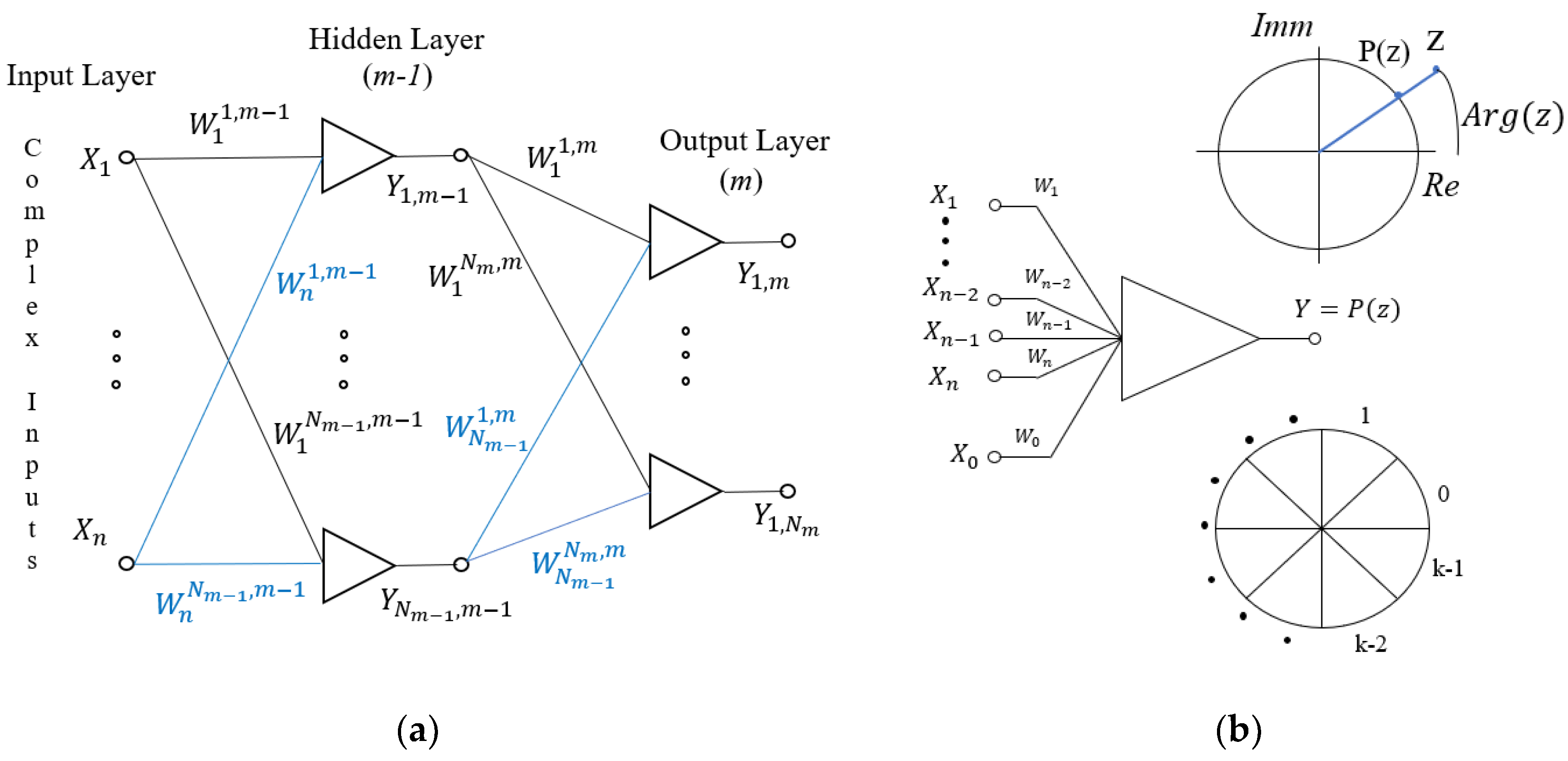
In the case of the diagnosis of DC–DC converters, currents, and voltages are extracted in a specific time interval at the ends of the passive components selected by the testability analysis. Consequently, mean values and ripples of the measured quantities are calculated and processed as shown in (4). As shown in Figure 1a, the neural classifier used in this case is constituted of three layers: the input layer, hidden layer, and output layer.
In the first layer, the complex inputs are created starting from the values belonging to the dataset matrix. Hence, they are connected to the hidden neurons through complex weights. These neurons are characterized by a continuous activation function,
where Arg(z) is the argument of the weighted sum calculated by (6),
in which is the i-th weight of the considered neuron and is the i-th input. In order to clarify the meaning of these terms, Figure 1b shows a graphical representation of the multi-valued neuron. Therefore, all inputs belonging to the same sample are used to calculate a weighted sum (6) for each hidden neuron. These neurons use the discrete activation Function (5), which generates an output on the unit circumference of the complex plane corresponding to the division of the weighted sum by its magnitude.
Therefore, MLMVN neurons have multiple inputs and one complex output located on the unit circle. When the final purpose is the classification of input patterns, each neuron belonging to the output layer divides the complex plane into k equal sectors and the following activation function is used,
where j is one of the possible k sectors and is the argument of the weighted sum. This means that the neurons belonging to the last layer are discrete and each output corresponds to the lower border of the sector that contains the weighted sum of the inputs.
During the training phase of the classifier, the values of the weights are corrected in order to minimize classification errors. These errors are complex numbers, each of which is calculated as the difference between the desired output and that obtained by processing specific inputs. In fact, MLMVN is based on a supervised learning algorithm and this means that the dataset matrix must contain the inputs and the corresponding desired output for each neuron in the last layer.
One of the most important advantages of the MLMVN compared to other machine learning methods is the absence of derivative terms in the training procedure. In fact, the backpropagation procedure is not based on the gradient calculation and the following formula is used,
where is the correction for the -th weight of the -th neuron belonging to the layer , is the corresponding learning rate, is the number of the inputs equal to the number of the outputs of the previous layer, is the magnitude of the weighted sum, is the output error, and is the conjugate-transposed of the input. This learning rule is used for the correction of the weights and is repeated for each sample () belonging to the dataset matrix. Therefore, the dataset matrix must contain numerous examples of all possible situations and their classification. The backpropagation procedure here described is an iterative method in which all corrections are calculated Ns times for each weight (training epoch).
Alternatively, algorithms based on linear least square (LLS) methods can be used in order to reduce the computational cost [49]. In this case, all output errors are saved in a specific matrix,
and the corrections of the weights are calculated by solving an oversized system of equations at the end of each training epoch. These solutions can be calculated through various techniques, such as Q-R decomposition or singular value decomposition (SVD). The system is oversized because the number of samples belonging to the dataset is higher than the number of corrections to be calculated. It can be written in a compact form as
and the solution obtained with the LLS method satisfies this condition
where the superscript indicates the number of the neuron taken into account, is the pseudo-inverse of the matrix and is its conjugate transpose. Moreover, the soft margin method is used to improve the classification rate, changing the target for each output to the bisector of the desired sector [50].
4.2. Diagnostic Procedure
The neural classifier described in the previous subsection is used to validate the selection of measurements based on the testability analysis. The main purpose is the diagnosis of parametric faults in DC–DC converters and the choice of test points plays a fundamental role in providing significant quantities to the MLMVN. In fact, the use of measures that have indistinguishable variations, when different malfunctions occur, is completely useless.
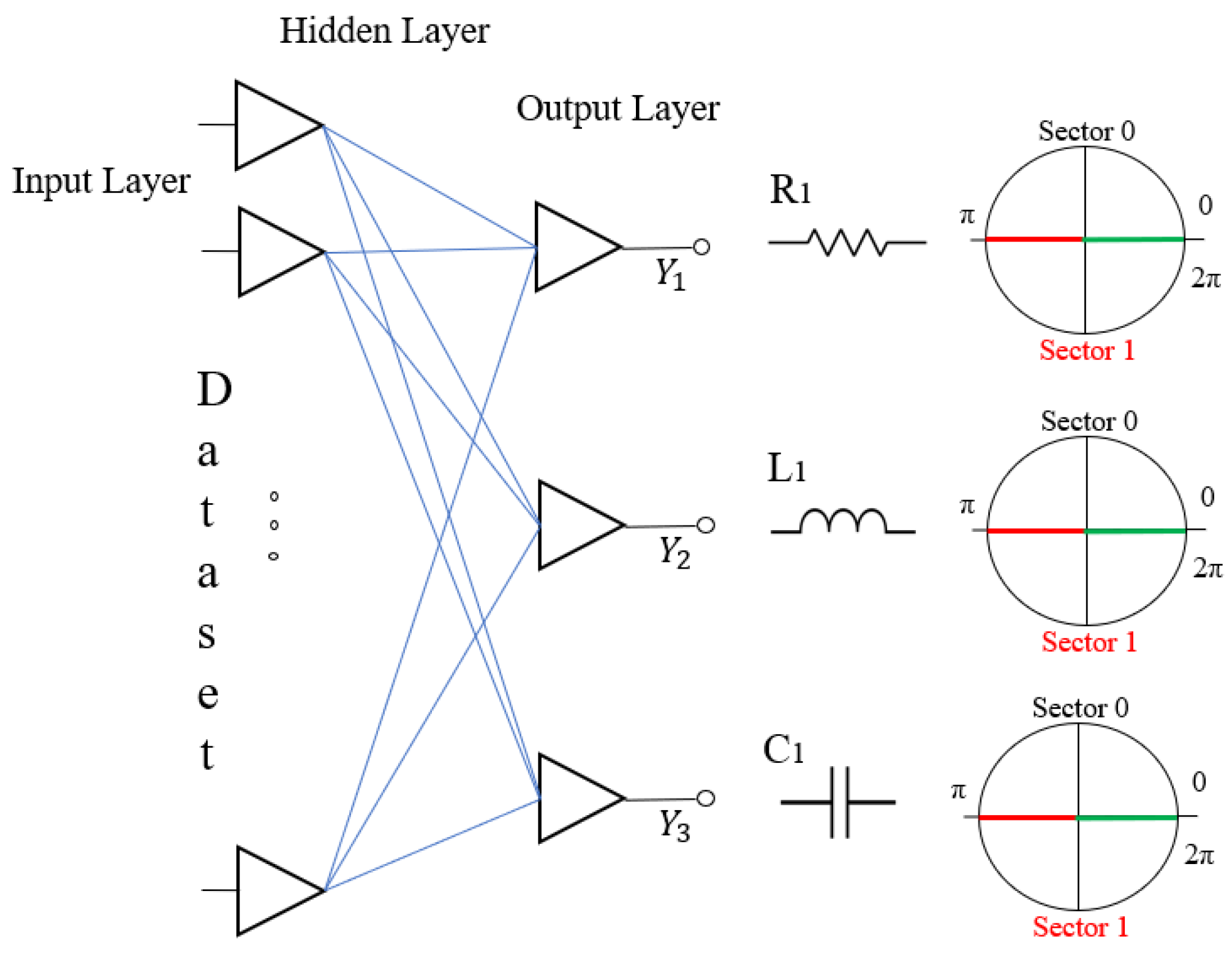
Since the objective is the detection and localization of malfunctions in a specific component, the number of fault classes depends on the number of passive elements. When the testability is maximum and the single failure hypothesis is assumed, each converter component can be considered faulty, but one at a time. Therefore, one neuron is used in the output layer of the MLMVN for each passive component that can be considered variable. These neurons are binary, because they must distinguish the nominal condition of each element from its malfunction condition. For example, Figure 2 describes the output layer of an MLMVN used to detect the state of health of three passive components.
Each neuron belonging to the output layer divides the complex plane into two sectors: the first of them corresponds to the upper half plane (0, π) and is encoded by the value 0, while the second sector is the lower half plane (π, 2π) and is encoded by the value 1. The term 0 is used to describe the nominal condition of the corresponding component and the number 1 is used to indicate its malfunction. When all outputs are equal to zero, the whole system is functioning correctly. Therefore, the diagnostic procedure can be summarized as follows:
- definition of the converter topology;
- definition of the nominal value for each passive component and application of a specific tolerance;
- testability analysis and subsequent selection of test points in order to classify as many components as possible;
- according to the testability analysis, the distinguishable components are considered as variable terms, while other components are fixed to their nominal values;
- creation of the neural classifier used as neurons in the output layer as the number of potentially faulty components;
- creation of the dataset matrix;
- learning phase of the MLMVN;
- validation and test phase.
5. Application Examples
5.1. Testability Analysis of a Buck Converter
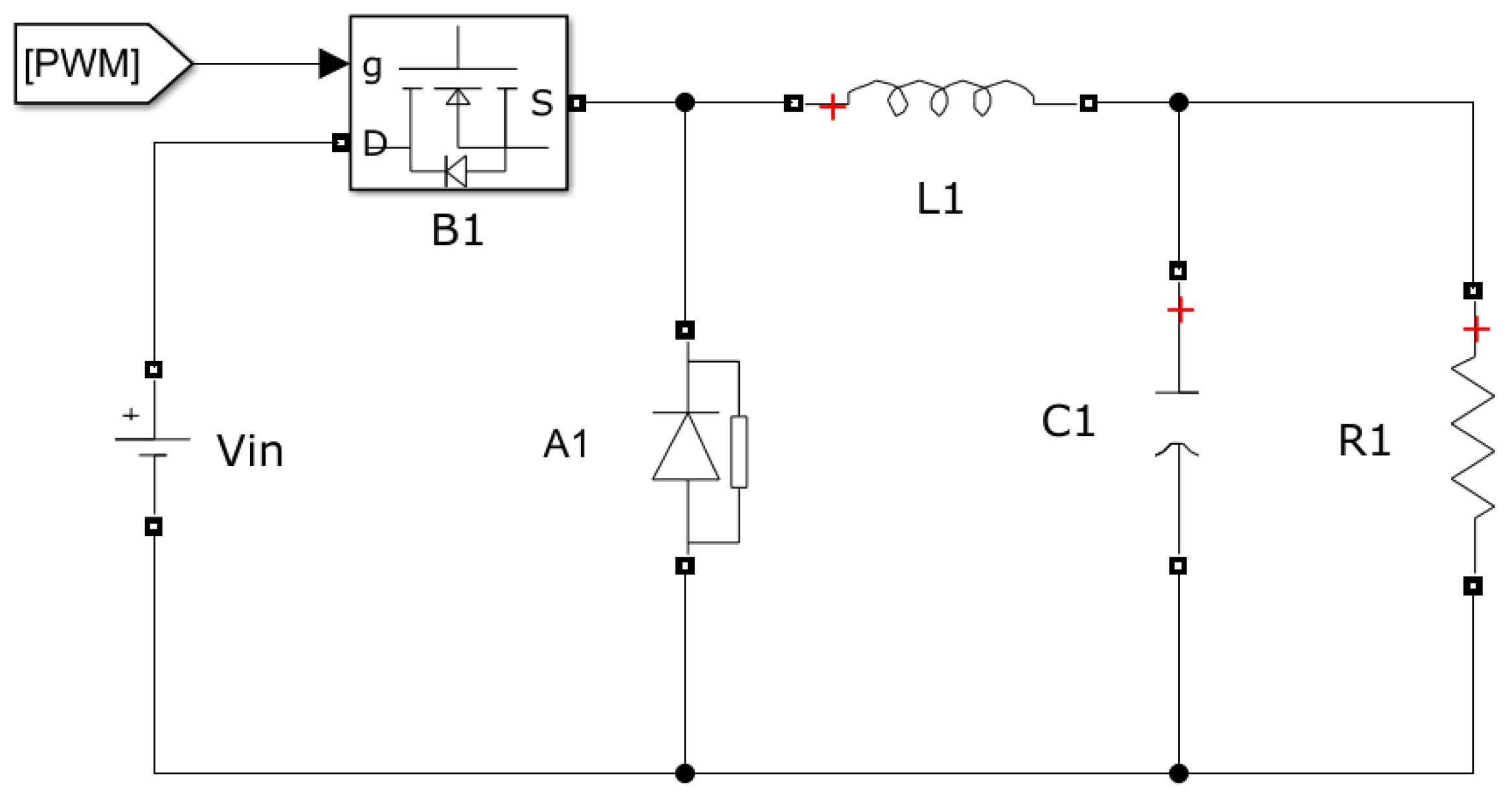
The first topology taken into consideration is a buck converter shown in Figure 3, in which there are three passive components: two reactive elements (L1 and C1) and a resistive load R1. This is a switching converter driven by a pulse width modulation (PWM) capable of reducing the input DC voltage with high efficiency [51]. The output voltage is measured at the ends of the resistive load and, in CCM, it can be calculated as
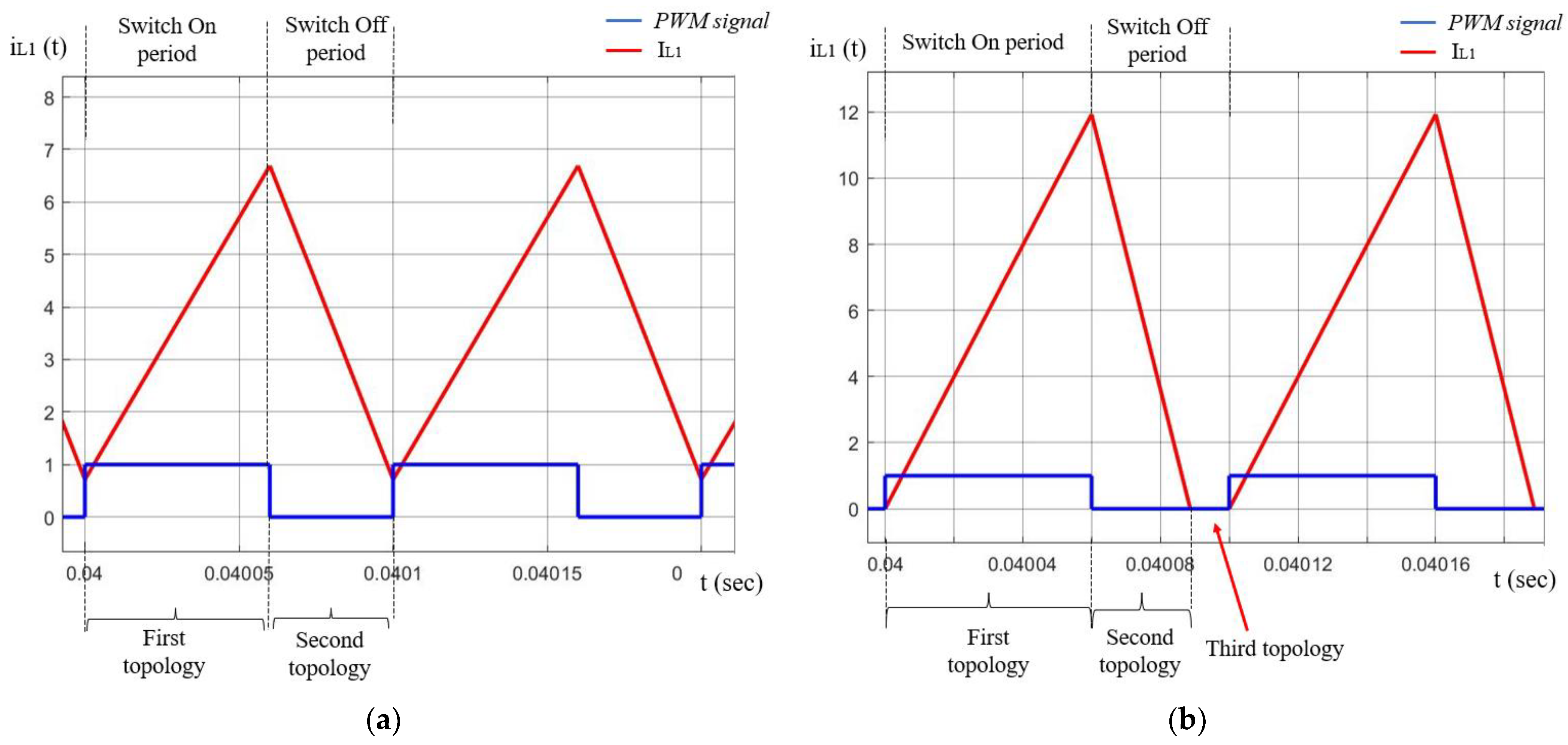
where D is the duty cycle of the PWM signal and is the DC source. During the operation of the converter, it is possible to distinguish two different periods: switch-on period and switch-off period. They are related to the state of the active components (B1 and A1), which are alternately conductive and interdicted. During the switch-on period, B1 is in conduction, while A1 is off; during the switch-off period, the state of the active elements is opposite.
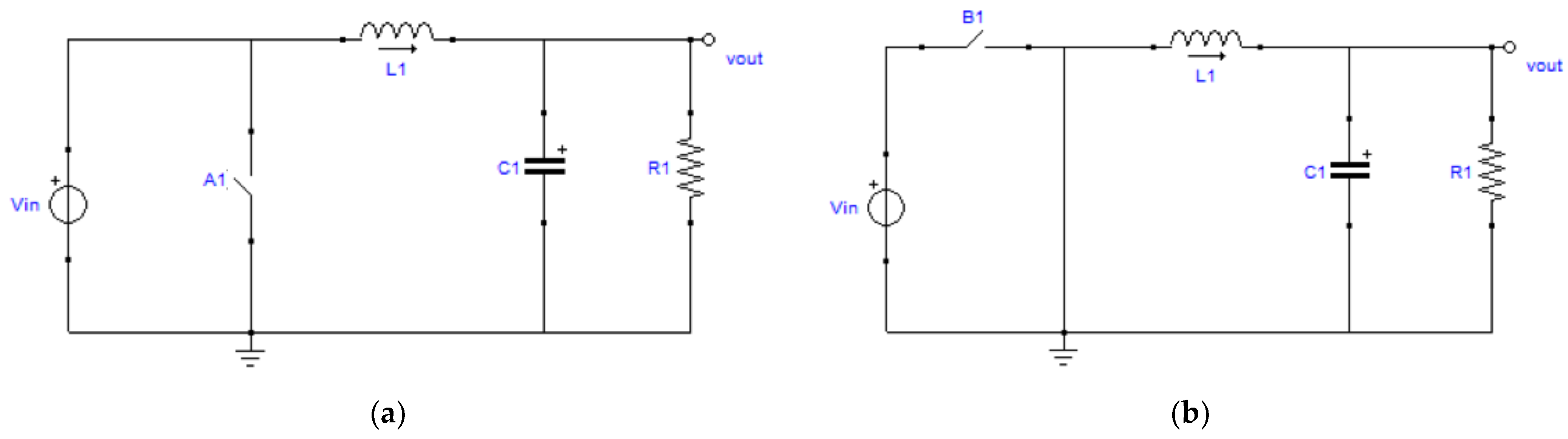
As said before, the time-varying nature of DC–DC converters makes the testability analysis more complex, because different topologies are obtained depending on the time interval taken into consideration. Figure 4 shows the two different circuit configurations obtained during the on period and the off period in CCM.
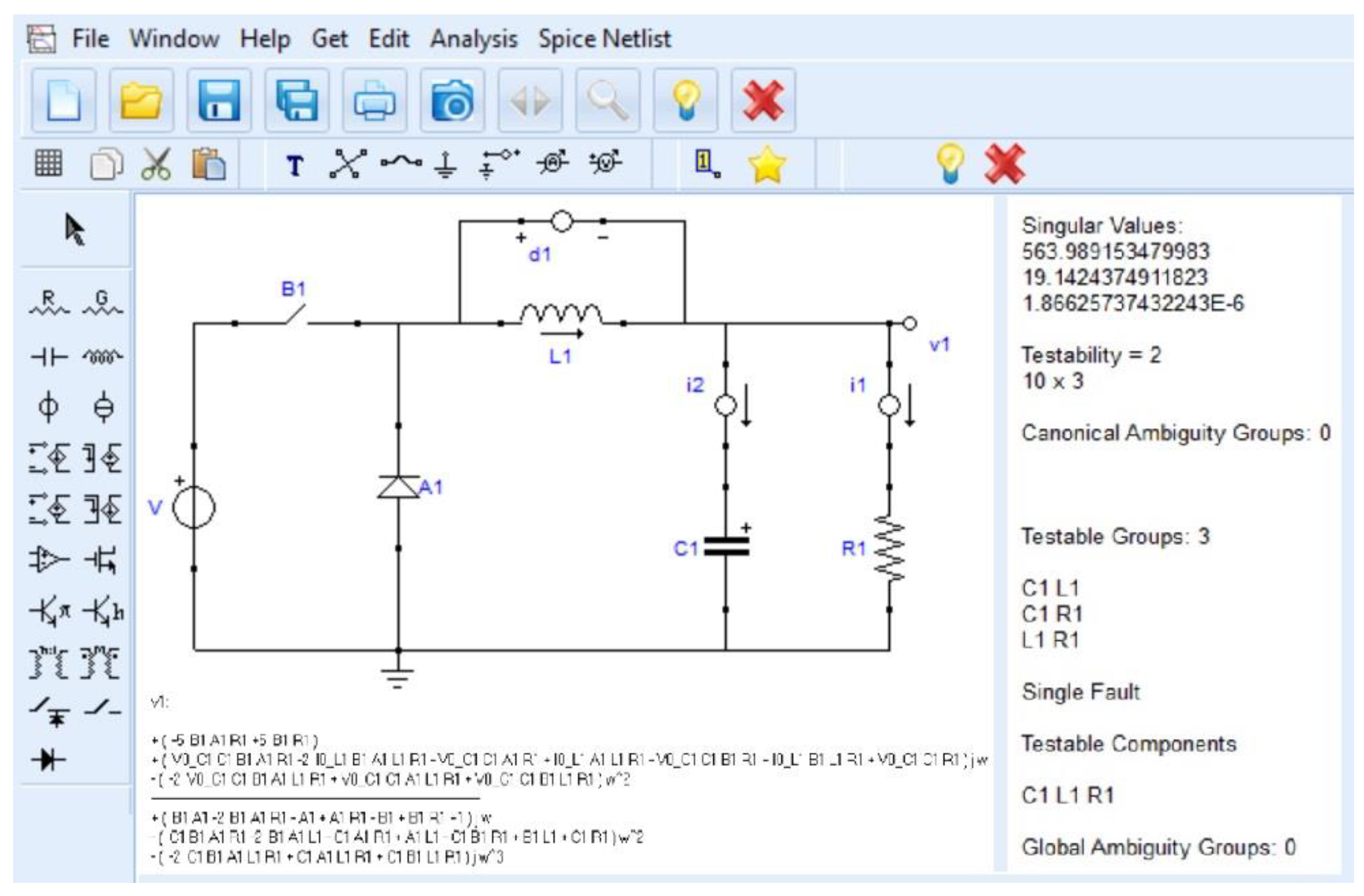
The first step for verifying the equivalence of the two approaches described in Section 3 is to evaluate the testability in the frequency domain using the TAPSLIN software (first version developed by the Department of Information Engineering, University of Florence, Florence, Italy). In this case, the symbolic form of the transfer functions relating to the two circuits of Figure 4a,b are analyzed individually, and the rank of the Jacobian matrix corresponds to the testability value. It should be noted that multiple test points can be used obtaining different transfer functions and testability levels.
The second step is the analysis of the converter in the time domain using the same test points. In this case, the Simulink/Simscape model of the buck converter is used to extract the voltage and current waveforms by varying the values of the passive components. Therefore, by processing these quantities, it is possible to create graphs in which the ripple is on the ordinate axis and the average value is on the abscissa axis.
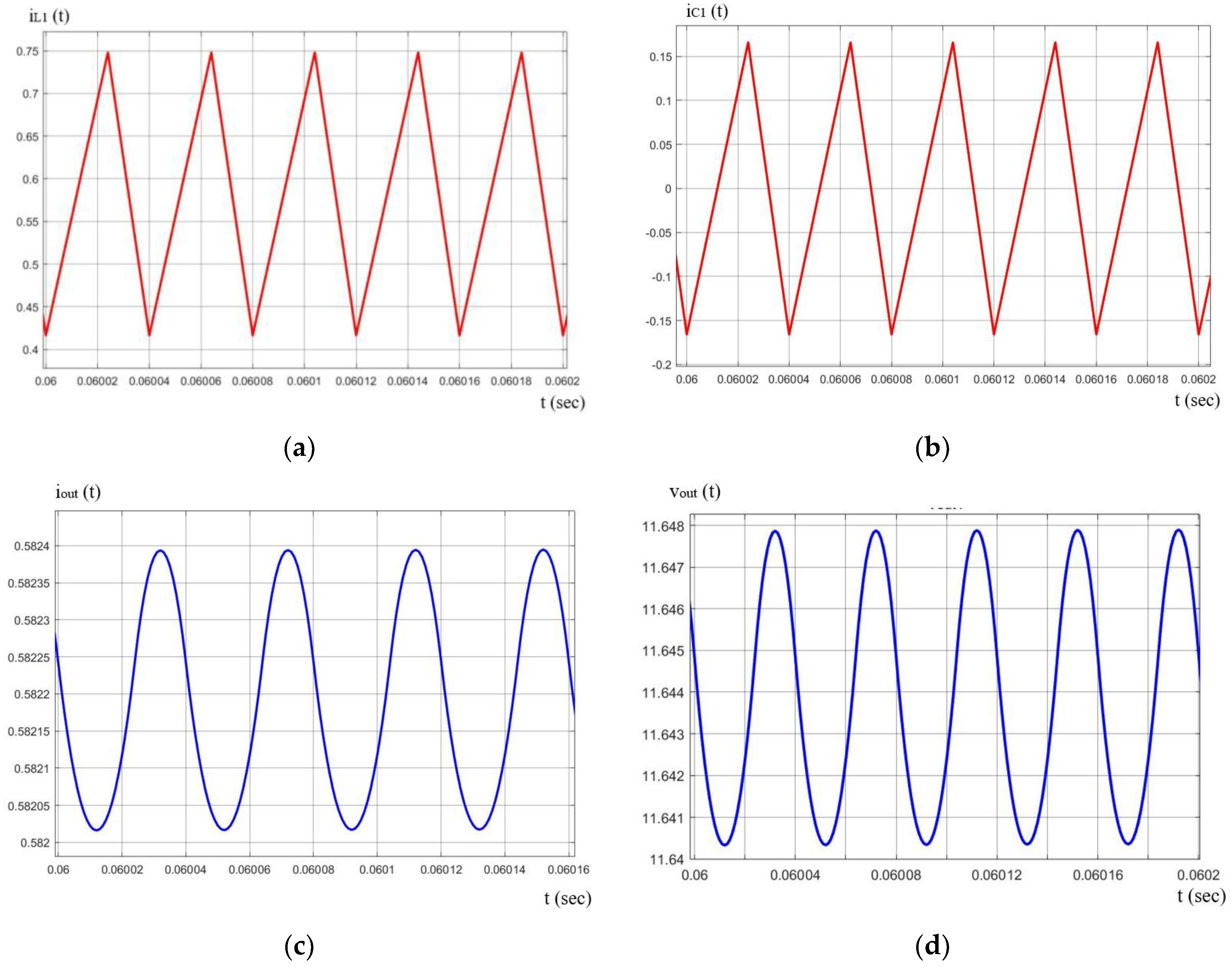
By analyzing these curves, it is possible to obtain information about testability and testable groups. In fact, when two or more curves are superimposed or very close together, the corresponding components cannot be considered faulty at the same time. Figure 5 shows some of the characteristic waveforms of the converter operation in CCM using a DC source of 20 V and D = 0.6.
5.1.1. First Method: Testability Analysis of a Buck Converter in the Frequency Domain
The results obtained through the TAPSLIN software are summarized in Table 1 (TG—i.e., Testable Group—is a parameter group that can be considered unknown). In this case, the test points taken into consideration allow the measurement of the output voltage and the capacitor current. By considering only one of them at a time, the analysis in the switch-on period and that in the off period show the same results—i.e., the test point related to the output voltage, as also the test point relevant to the capacitor current, give a result in terms of testability equal to 2. The same situation occurs if the two test points are simultaneously considered. Figure 6 shows the TAPSLIN user interface and the testability analysis performed for the buck converter.
In this situation, there are no differences in the testability analysis for the two topologies shown in Figure 4 and the testability level is lower than the total number of passive components. This means that one of the elements must be fixed to its nominal value and it cannot be considered as a faulty component during the diagnostic procedure.
In order to increase the testability value, it is necessary to modify the test points considered. For example, by simultaneously using the output voltage and the inductor current as measurements, it is possible to obtain the maximum testability. Furthermore, this choice shows a difference between the testability calculated during the switch-on period and that calculated using the second topology (Figure 4b).
Table 2 summarizes these results.
5.1.2. Second Method: Testability Analysis of a Buck Converter in the Time Domain
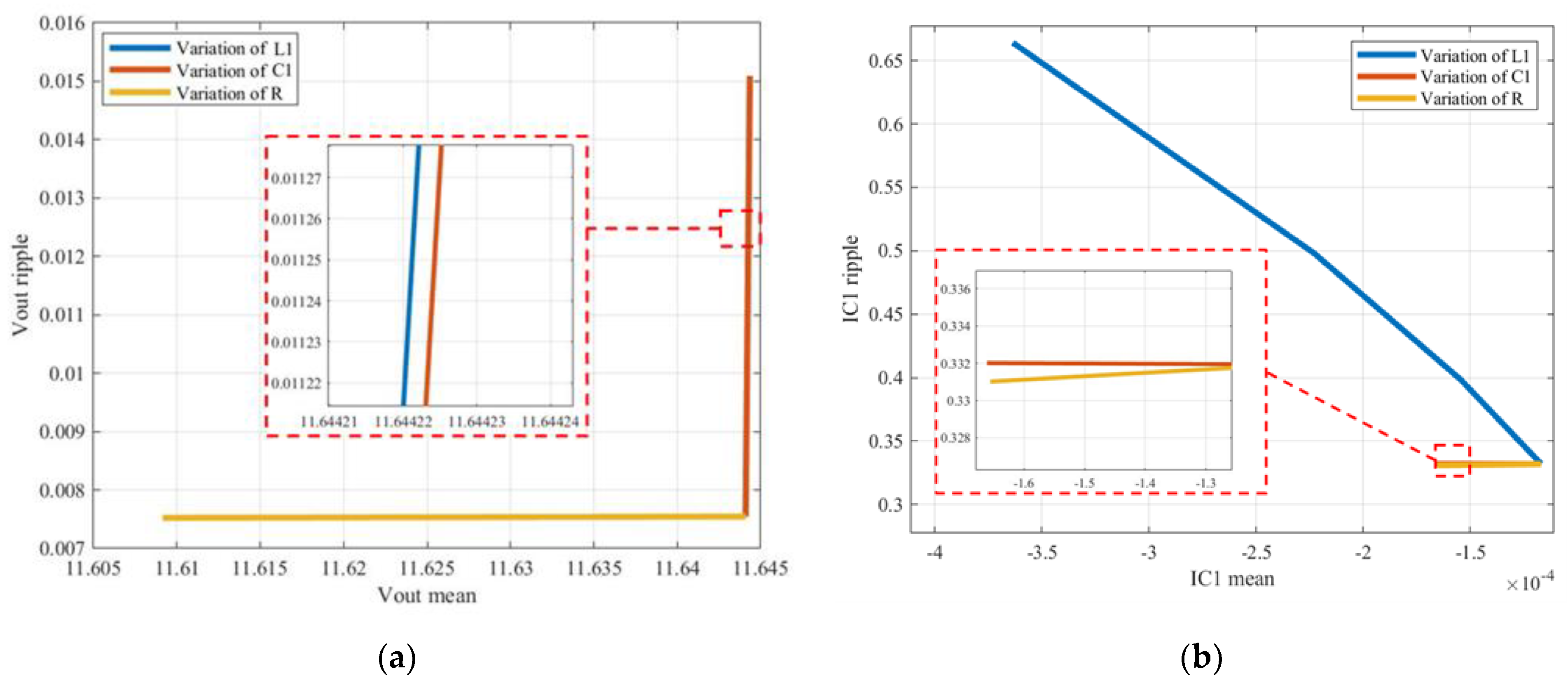
The second approach for the testability assessment is based on the Simulink/Simscape model of the buck converter. Several simulations are carried out by varying the values of the passive components one at a time. The selected measurements are then extracted when the steady state condition is reached by the converter. Finally, the measured quantities are processed to obtain the ripple and the mean value. In order to validate the first results obtained in the previous subsection, the output voltage and the current on the capacitor are considered. Figure 7 shows the corresponding testability curves.
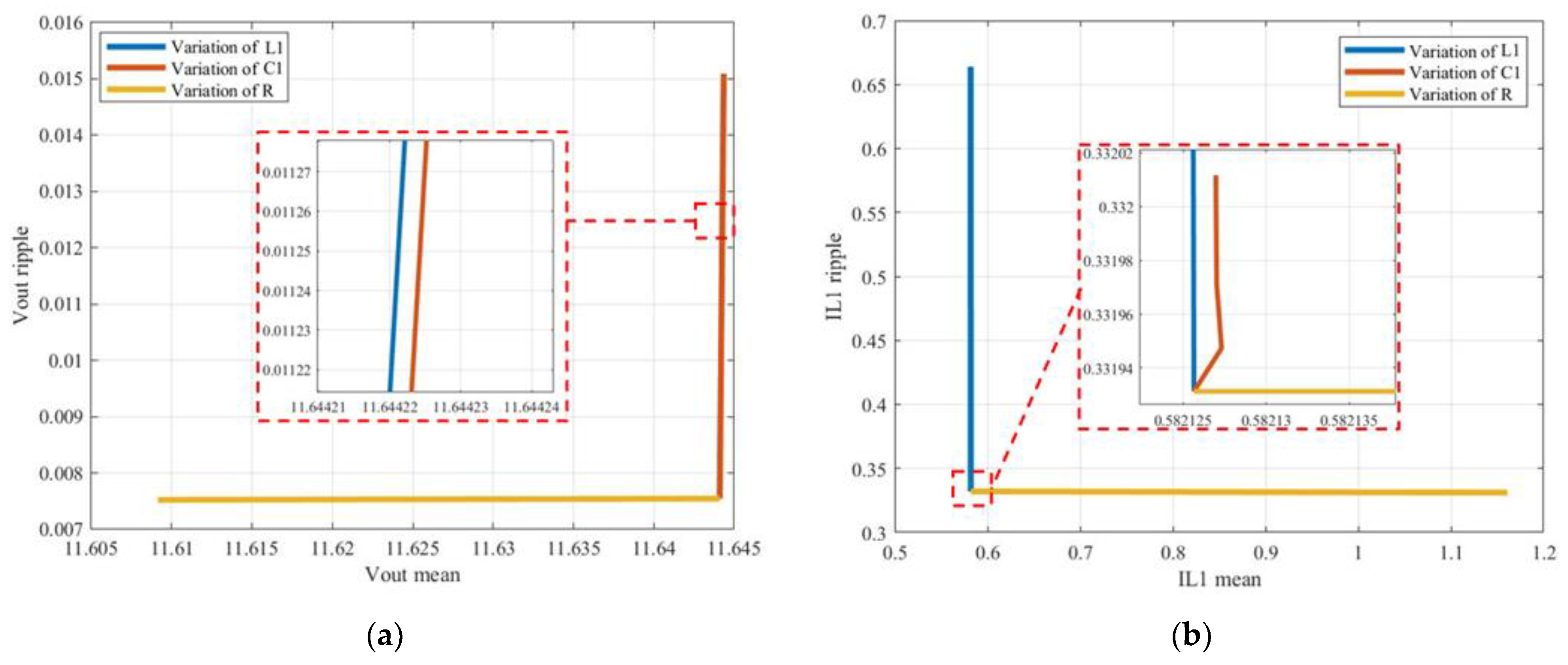
The curves presented in Figure 7 show that the testability value is 2 and each pair of passive components can be considered as a testable group. The curves obtained during the switch-off period offer the same results and confirm the content of Table 1. As regards the use of the output voltage and current on the inductor as test points, the curves shown in Figure 8 are obtained during the switch-on period. In this case, the effect of the variations of C1 in Figure 8b is absolutely negligible. This determines maximum testability and, consequently, there is only one testable group containing all three passive components, if both the test points are simultaneously considered.
5.2. Testability Analysis of a Boost Converter with Parasitic Resistances
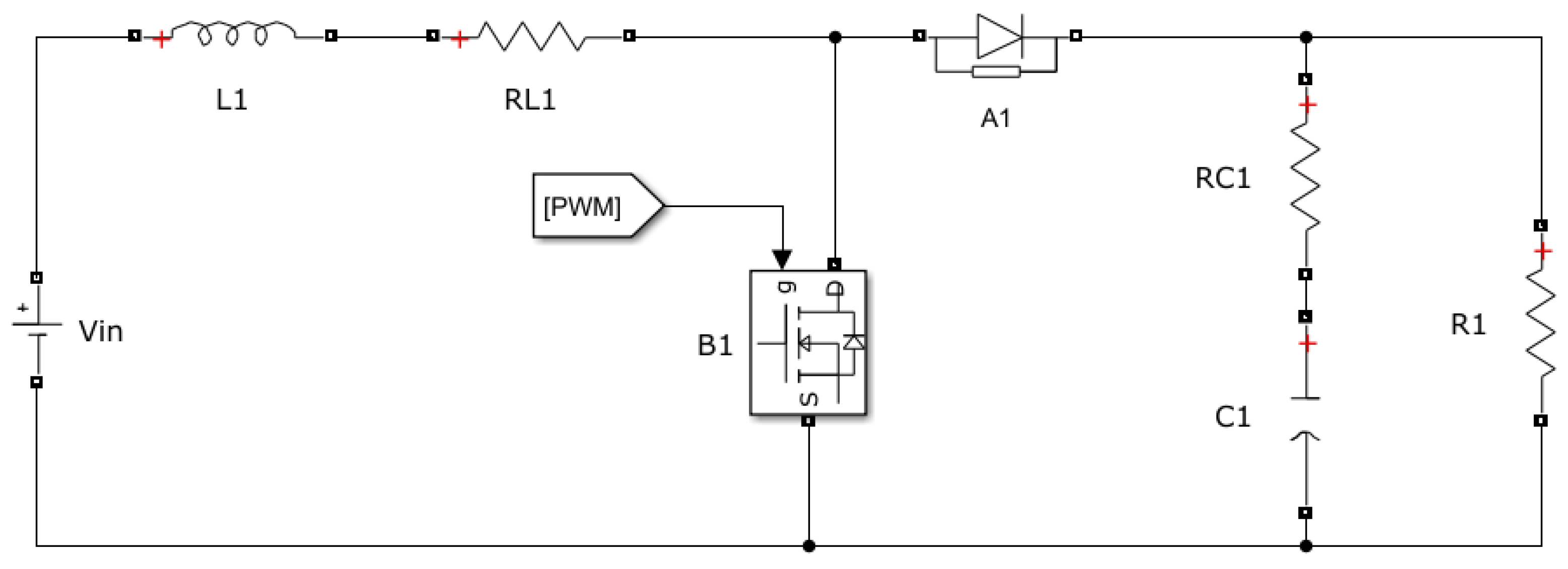
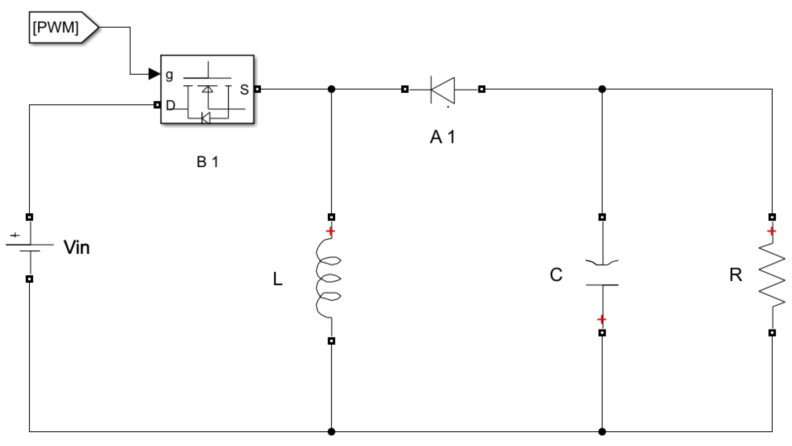
One of the most important aspects in the new graphical method here proposed is its easy application on different circuit topologies. Furthermore, there are no restrictions on the total number of passive elements that can be taken into consideration. This plays a fundamental role when parasitic effects must be included in the diagnostic procedure. In this subsection, a boost converter is analyzed, which is used in many devices powered by a battery in order to increase the voltage level. The circuit taken into consideration is presented in Figure 9, in which parasitic resistances are introduced for both the inductor and the capacitor.
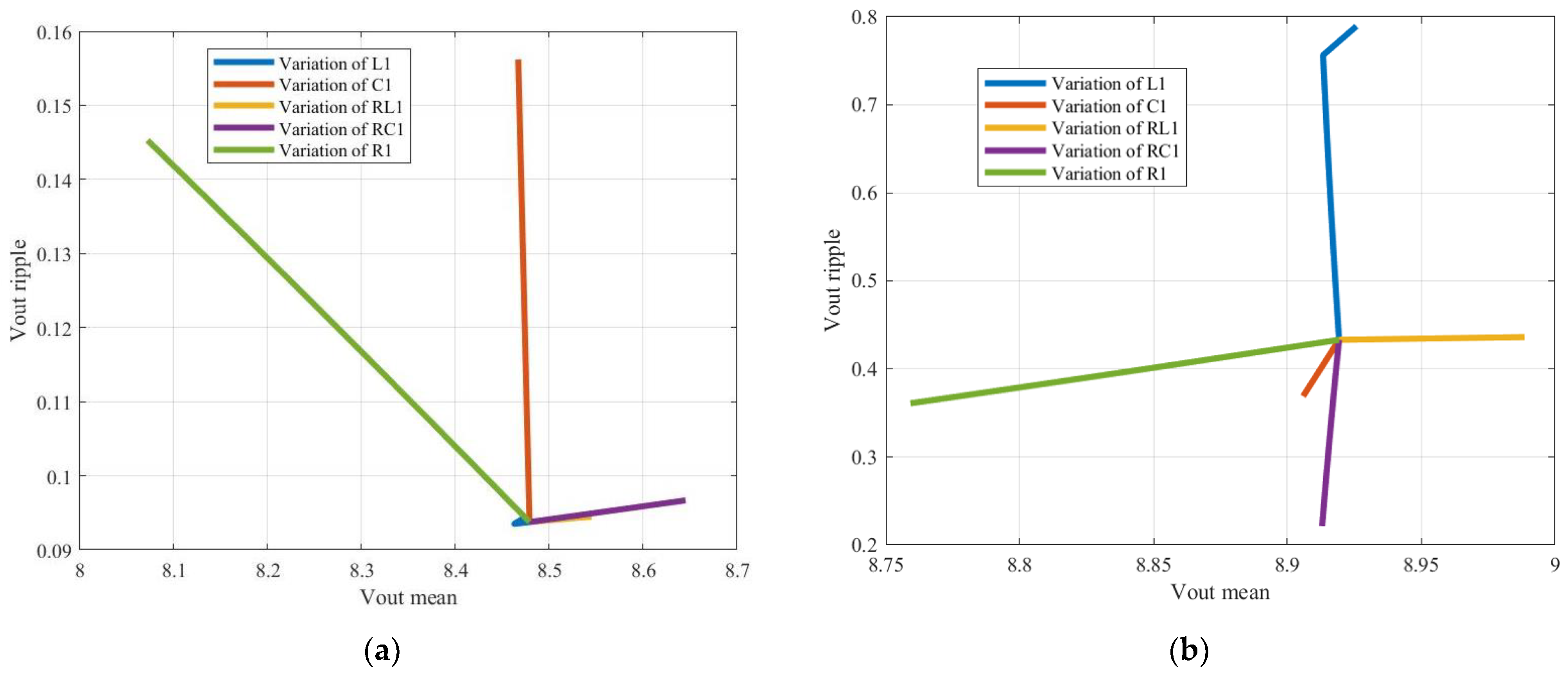
The first simulation presented for this converter is performed considering the output voltage as a single test point during the switch-on period. As shown in Figure 10a, the effects produced by R1 and C1 are easily identifiable, while the consequence of changes in L1 cannot be detected and those introduced by RL1 and RC1 are not distinguishable. Therefore, by setting the values of L1 and RL1 (or alternatively RC1), it is possible to diagnose three parametric faults. This means that the testability level is 3.
By changing the switching period considered, the curves shown in Figure 10b are obtained and the testability is equal to the maximum value 5. However, the effects induced by changes in C1 are very small and their identification depends on the sensitivity of the measuring instrument.
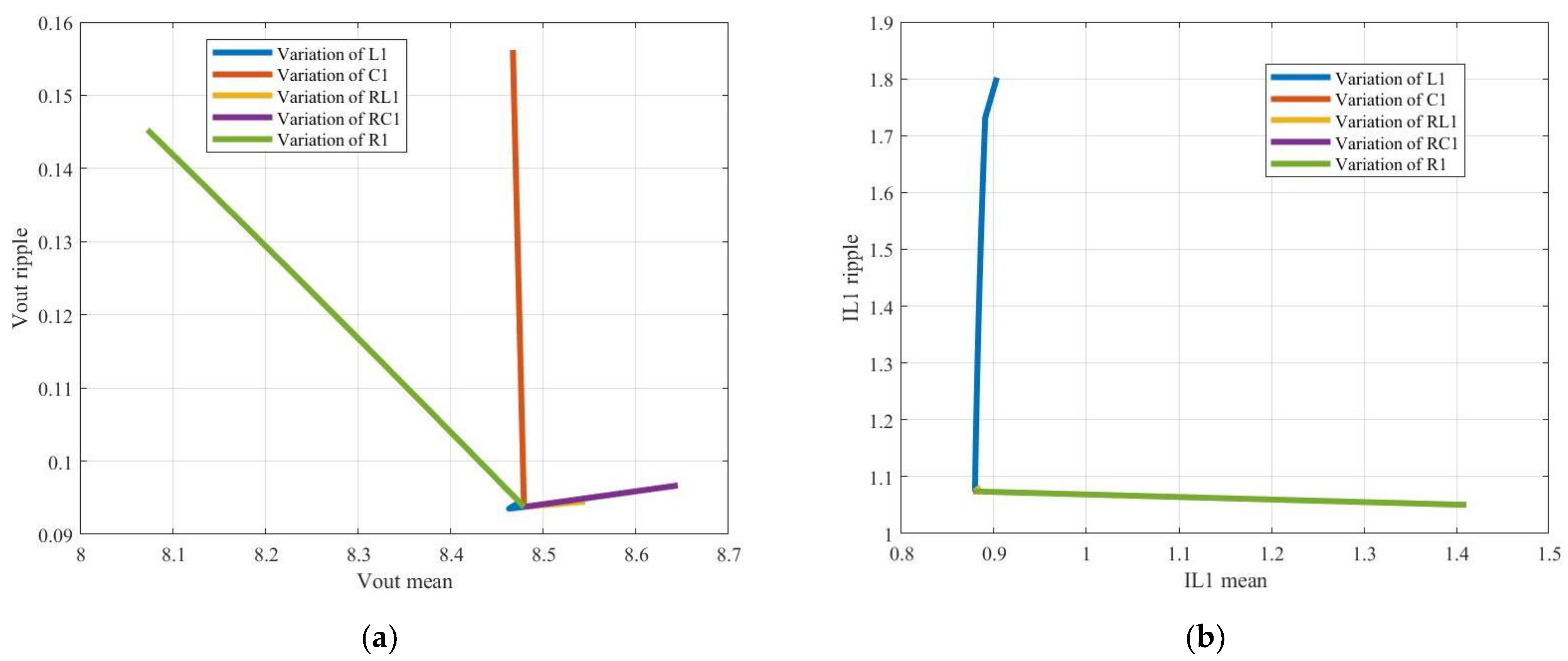
To increase testability during the switch-on period, it is necessary to use additional test points. For example, by introducing the measurement of the current on the inductor, it is possible to increase the testability from 3 to 4. In fact, in this case the variations of L1 become distinguishable. Figure 11 shows this condition. It should be noted that increasing the number of test points means increasing the intrusive level of the diagnosis system. This means that monitoring the off period of the boost converter offers significant benefits.
5.3. Testability Assessment of a Buck–Boost Converter
To conclude the discussion of the most common power converters, in this subsection a buck–boost converter is considered. The basic topology of this circuit is shown in Figure 12 and the nominal values of the electrical components are presented in Table 3. The variation range used to create the testability curves extends up to a reduction of 70% starting from these values.
Since the inverting topology is considered, the voltage gain G of the converter in CCM is expressed by Formula (13),
where D is the duty cycle used. Regarding the limiting level of the inductance between CCM and DCM, it can be calculated through the Formula (14),
where T is the switching period, Vin is the input voltage, and IO is the output current. As for the initial condition on parameters L and C, it should be noted that both the voltage on the capacitor and the current through the inductor are zero.
The graphical study of testability for a buck–boost converter in the time domain is carried out using the Simulink model shown in Figure 12. To present a complete view of the possible situations, the testability curves obtained on all measurable electrical quantities and in all switching periods are presented.
It is necessary to highlight that in addition to the two topologies corresponding to the on and off periods, it is possible to carry out the testability study in a third topology, corresponding to the DCM situation. In fact, if in the off period the current on the inductor becomes zero before the next commutation, a new circuit topology is obtained.
Figure 13a shows the situation in CCM, where only two topologies can be examined: the first one in correspondence with the on period and the second one in correspondence with the off period. Figure 13b indicates the presence of the third topology during the off period of the DCM operation.
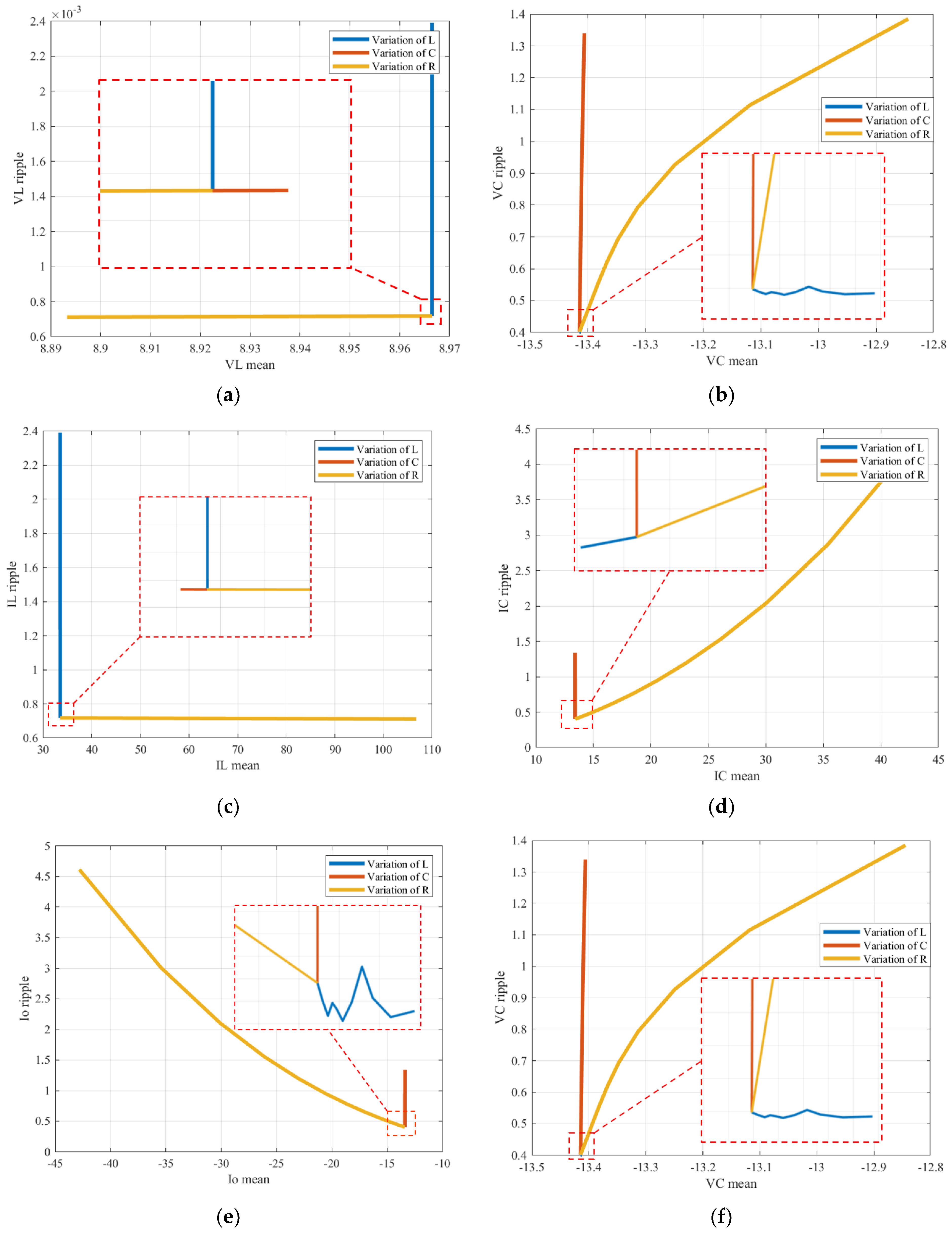
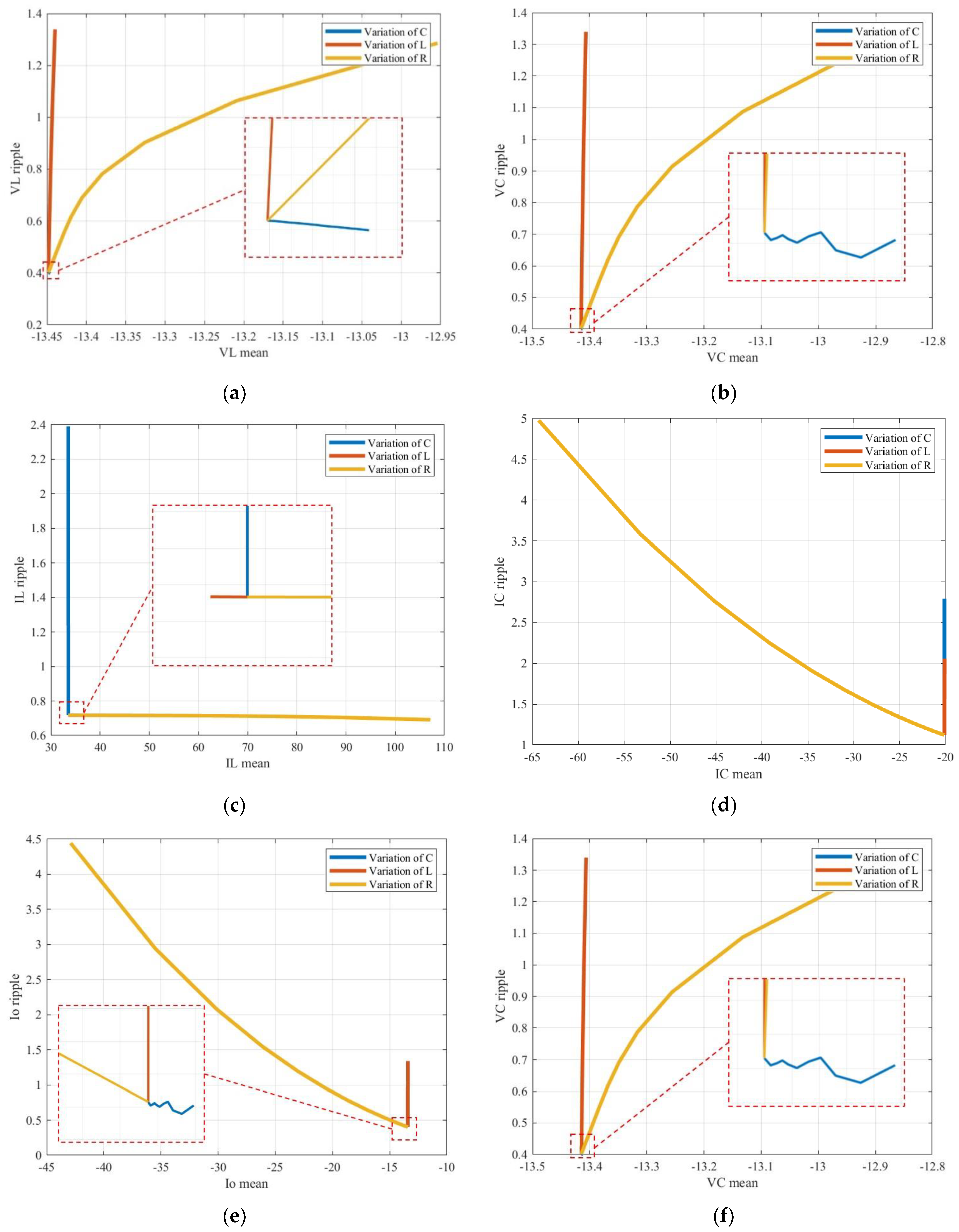
Figure 14 a–d shows the testability curves obtained during the switch-on period in CCM, while Figure 15 a–d refers to the switch-off period in the same conduction mode.
The curves obtained in this case confirm the possibility of having maximum testability by choosing at least two proper measures. For example, the use of the output voltage and the current on the inductor guarantees the identification of all possible malfunctions.
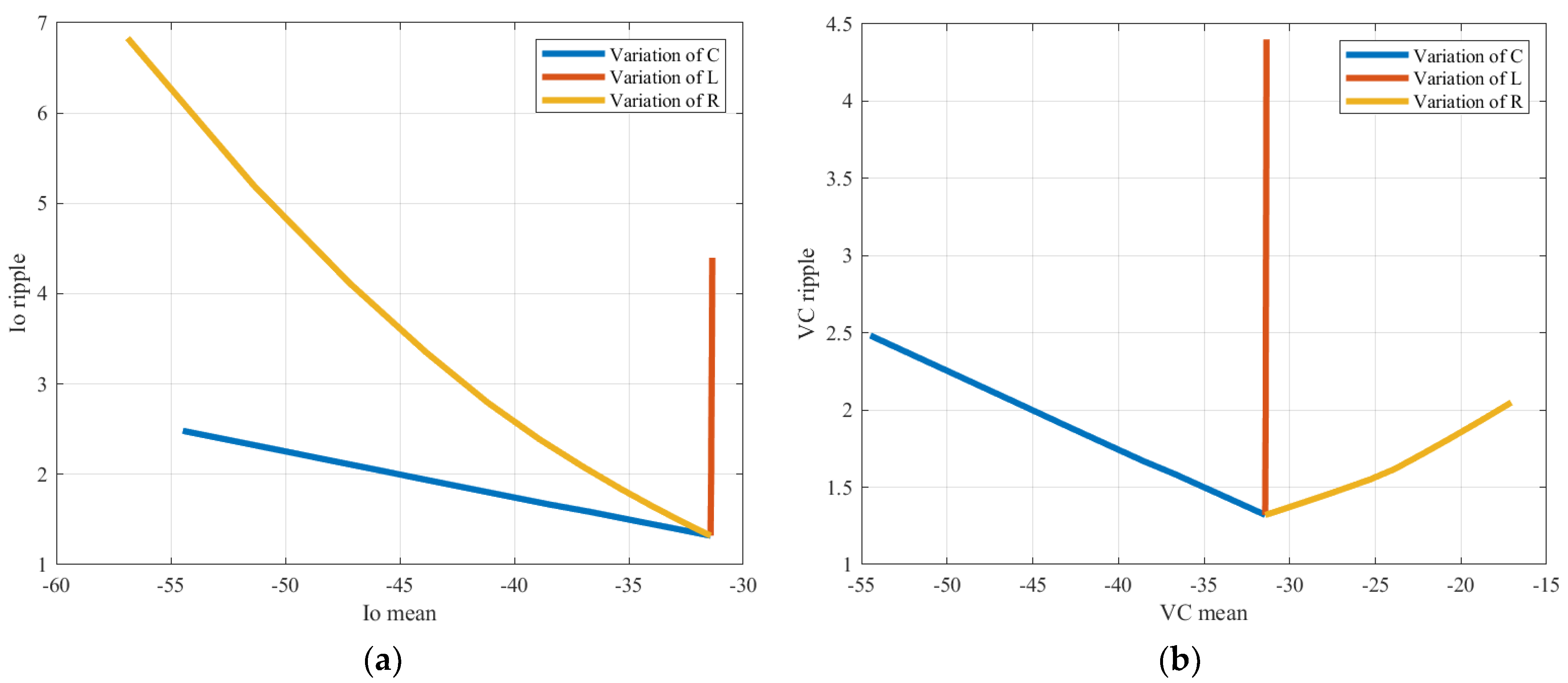
As for the third topology, it is possible to achieve maximum testability using only one measure. For example, Figure 16 shows that—by using the output voltage or the output current individually—it is possible to realize a complete monitoring of the passive components in a buck–boost converter.
6. Classification Results
Fault Diagnosis in a SEPIC Converter
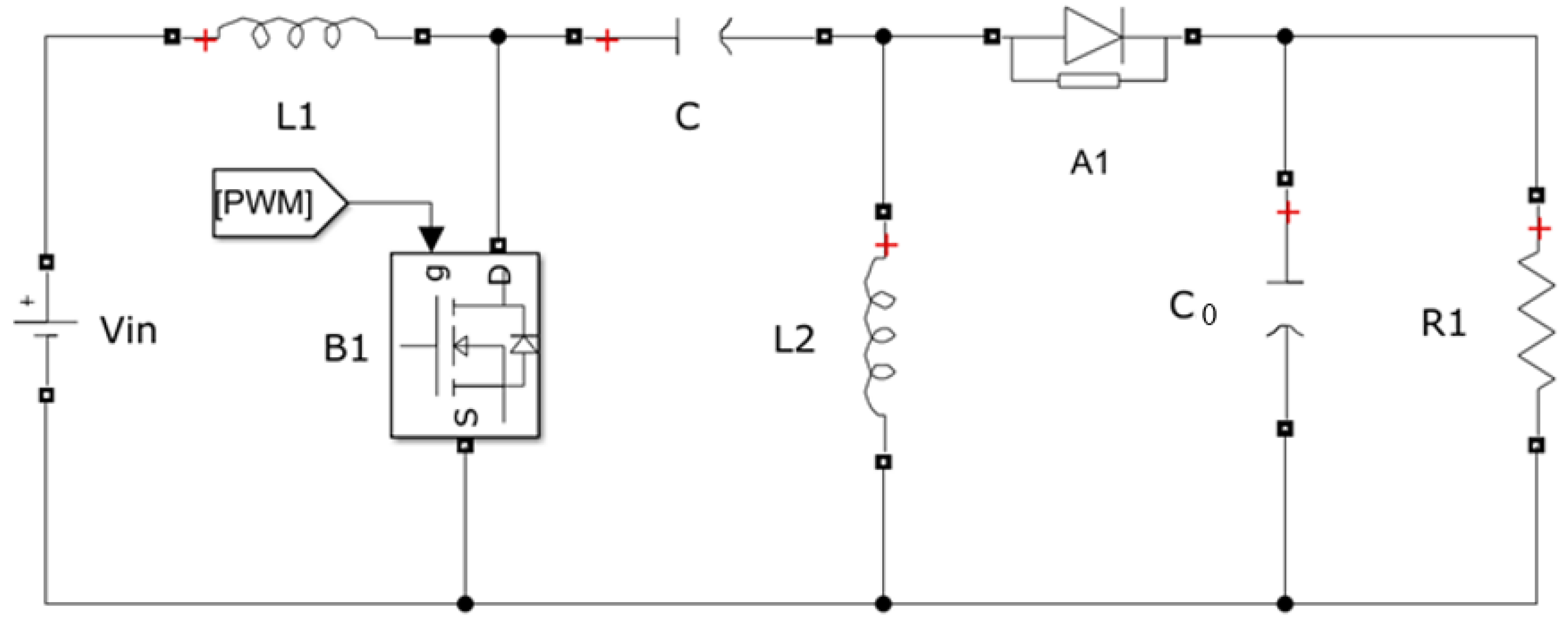
To show a complete diagnosis procedure, from the testability study to the classification of components by MLMVN, a SEPIC converter is considered in this section. This converter is a step-up/step-down circuit with non-inverted output and this represents one of the main advantages of the SEPIC converter compared to other types of buck–boost converters. Furthermore, thanks to the presence of a series capacitor, the SEPIC converter offers isolation between output and input. Figure 17 shows the circuit topology of this converter.
The converter components have been dimensioned as shown in [52] ensuring an output ripple of less than 5% during normal operation. The main objective of the diagnostic method is to detect variations of these elements beyond a tolerance of 10% with respect to nominal values.
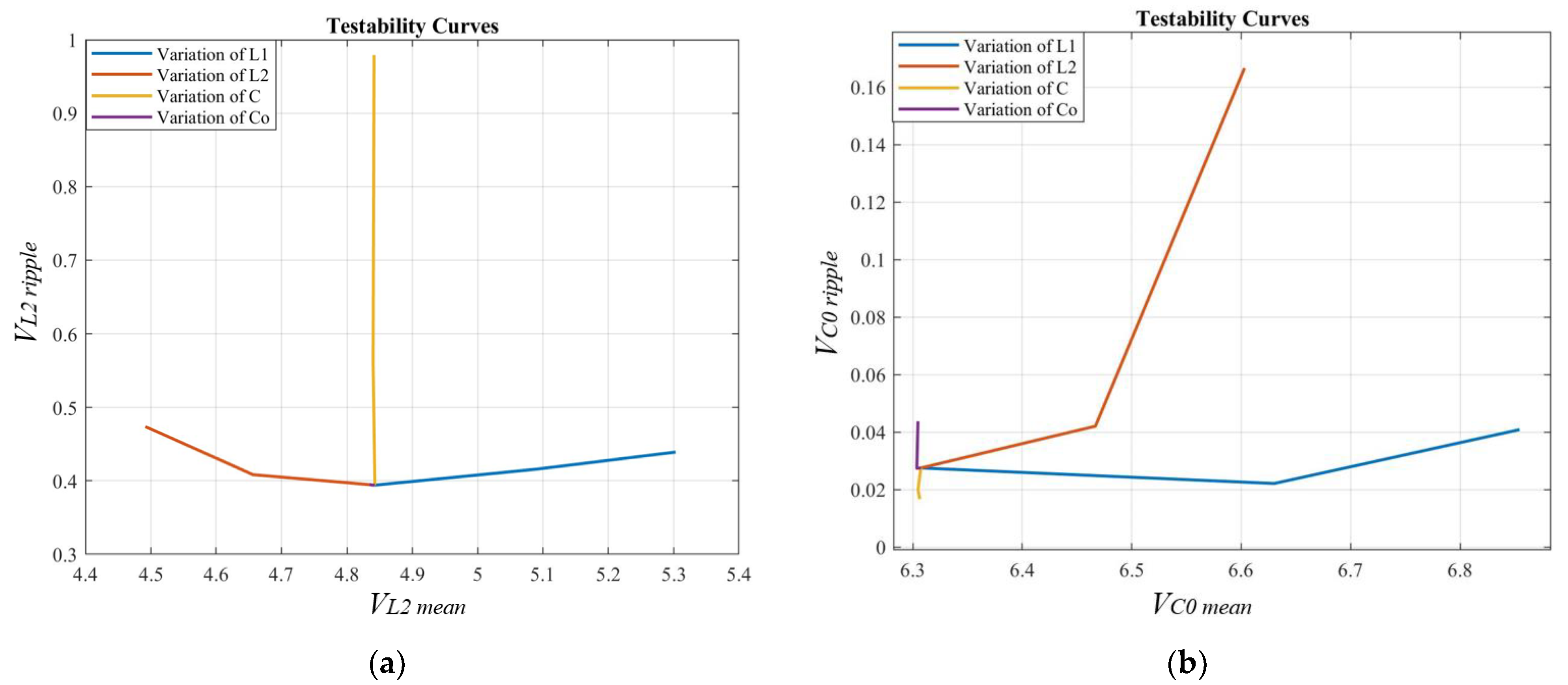
In this case, four potentially faulty components are considered: L1, L2, C, C0. Before training the neural classifier, it is necessary to define what measurements are needed. Therefore, the Simulink/Simscape model of the converter is used. The four components are varied starting from the nominal value until a reduction of 70% is reached. A simulation is carried out for each of these values by bringing the converter to the steady state. By analyzing the obtained results, it is possible to choose the measures that eliminate ambiguities and make all four components testable. The results relevant to the best test points are shown in Figure 18: they are the voltage on L2 and the voltage on C0. It should be noted that other measurements would also enable reaching the maximum testability, but, in this case, the voltages are chosen because they can be practically made with a less intrusive level. As it can be noted in Figure 18b, the curves relevant to each component are present, then the testability is maximum—i.e., equal to 4—with the only voltage on C0 as test point. However, the curve of C—completely distinguishable in Figure 18a—is very little in Figure 18b, so it is preferable to consider two test points.
Once the measurements have been chosen on the basis of the testability analysis, it is necessary to create a dataset matrix for training the neural classifier. As mentioned before, a multilayer neural network with multivalued neurons is used. Therefore, real measures are used as phases of unit module complex numbers, which are used as input to the classifier. Since the testability analysis takes into account the ripple and the mean value of each quantity, these characteristics belong to the dataset (15),
where, for example, is the first sample of the mean value of the voltage across L2 and is its ripple. The last element of each row in the dataset matrix is the number of the corresponding fault class. These values are defined as shown in Table 4.
NS simulations of the Simulink/Simscape model are performed to create the dataset matrix by modifying the values of the passive elements. When class 0 is simulated, each component of the converter is randomly selected within the range defined by the nominal value and a tolerance of ±10%. When the malfunction condition on a component is simulated, its value can have a maximum reduction of 70% from the nominal value. In this paper, 50 samples for each fault class are used and this means that NS = 250.
Before training the MLMVN, it is necessary to convert the indices of the failure classes into the desired outputs for the neurons belonging to the last layer. As stated in Section 4, one discrete neuron is used in the output layer of the classifier for each passive element. Since binary neurons are considered, the output corresponding to the nominal condition is the upper half plane (value 0), while that of the malfunction condition is the lower half plane (value 1). Consequently, each fault class is a specific combination of four binary numbers (Table 5). Therefore, the four complex numbers present in each row of the dataset (15) are considered as phases of complex numbers having a magnitude equal to 1 and are processed by the neural network. The neurons of the hidden layer generate outputs on the unit circle that correspond to the inputs of the output level. The neurons of this layer are binary and produce an output equal to 1 or equal to 0 according to the Equation (7). Therefore, there is a combination of four outputs, in which only one must be equal to 1. If the combination of the outputs does not correspond to the desired one (Table 5), one error is calculated for each neuron and proceed with the backpropagation described in Section 4. When the converter works in a wrong way, a combination other than four zeros is obtained at the output of the neural network, because at least one of the weighted sums falls into the negative half plane. This allows the detection of the problem and the localization of the faulty component. It should be noted that the ‘winner takes all’ rule is used in the case of two outputs equal to 1. In the case of the soft margin technique, this method keeps at a high level only the output closest to the bisector of the desired sector.
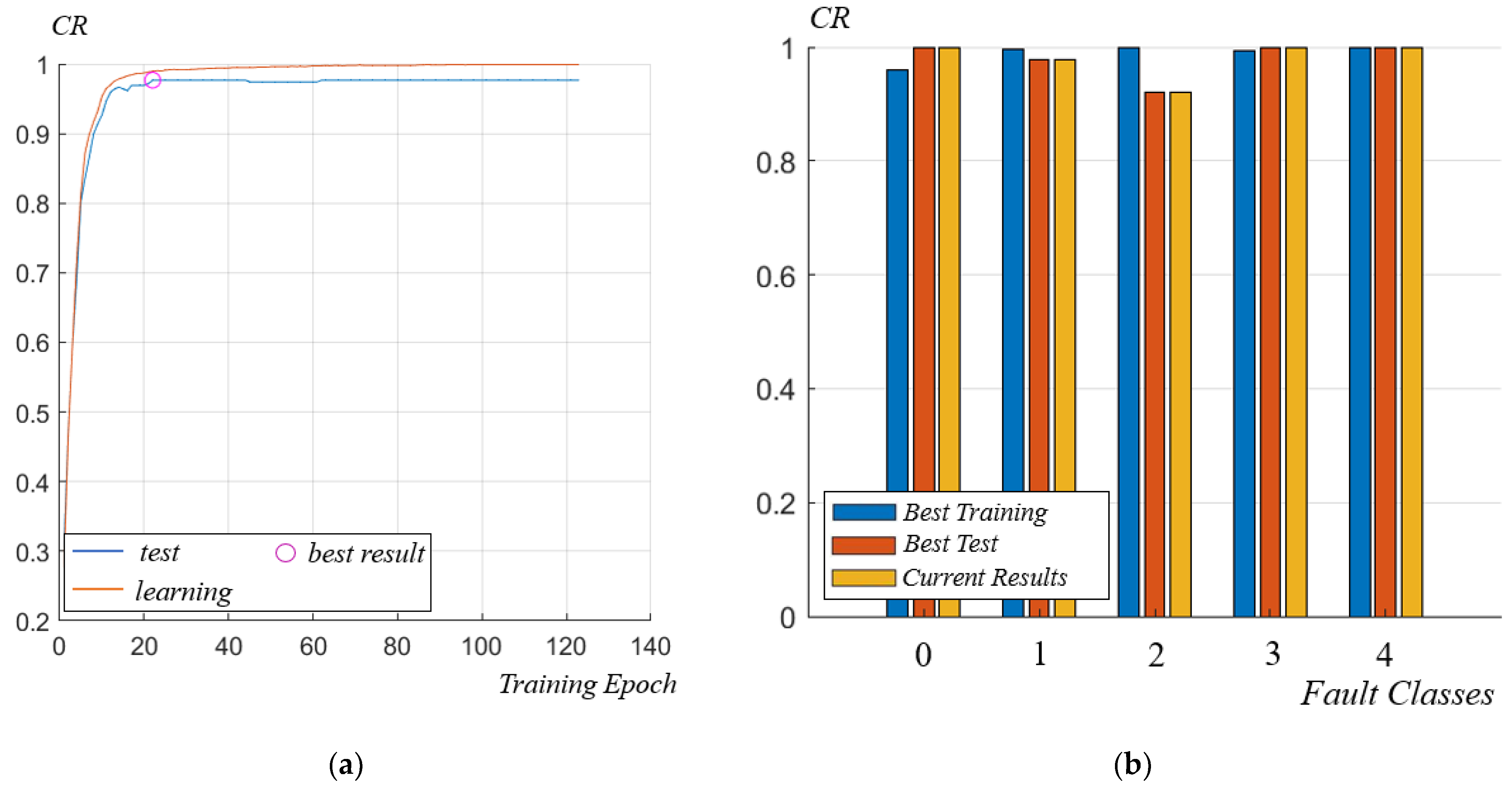
Finally, it is possible to train the neural classifier. Figure 19 shows the classification rate (CR) obtained using 70 neurons in the hidden layer. The training procedure has been performed using the hold out validation technique, this means that 80% of the data belonging to the dataset are used for the correction of the weights, while the remaining 20% is used to verify the performance. For this reason, the classification rate can be assessed in two different stages: learning phase and test phase.
The classification results obtained are excellent and guarantee the possibility of identifying parametric failures while preventing catastrophic ones. In this way, it is possible to organize maintenance operations, reducing recovery times and increasing the reliability of the converter. Finally, these excellent results validate the selection of measurements based on the graphical testability assessment. Table 6 summarizes all the classification results.
As mentioned above, these results are obtained through a holdout validation, in which 80% of the data is used during the training phase and the remaining 20% is used for validation. In order to propose a more accurate assessment of the performance, it is possible to repeat the hold out validation five times by modifying the data used for training and validation at the end of each process. In this way, each sample is used in both phases and the analysis of the results is more accurate. This method is called cross validation and, in this case, confirms the excellent performances shown in Table 6 and the fact that the number of false positive errors is greater than false negative ones. This is a very important aspect in industrial applications because false negative errors make it impossible to detect malfunctions and can lead to catastrophic consequences by putting the converter out of service. At each stage of training, class 0 has the lowest classification rate and there are some incorrect classifications between class 1 and class 3. Mistakes made on class 0 are defined as false positives, while errors between class 1 and class 3 only produce an incorrect localization of the problem. False negatives are therefore rare events and occur when one of the classes from 1 to 4 is incorrectly classified as class 0. Analyzing the data obtained with the cross validation, it can be noted that the false negative rate is about 2% during the phase of training.
Finally, other neural algorithms are trained using the same dataset in order to compare the MLMVM performances. Table 7 summarizes the percentual classification rate (CR%) of the considered classifiers. Several algorithms based on different theoretical approaches are considered: Bayesian classifier, decision tree based classifiers, K-nearest neighbor (KNN) classifiers, and support vector machine. It can be noted that the MLMVN guarantees the best performance in terms of classification rate. However, the choice of test points on the basis of the testability study guarantees excellent results with other classifiers as well. Therefore, the graphical method plays a fundamental role because it facilitates the evaluation of testability.
7. Conclusions
The new method for the testability evaluation proposed in this paper is based on time domain measurements of voltages and currents. It allows the selection of test points without ambiguities by reducing the intrusive level and ensuring the correct operation of the diagnostic system. The main advantage of this approach is the possibility to determine the testability level from a graphical point of view. This facilitates the study of time-variant circuits, such as DC–DC converters, which have different topologies depending on the time interval taken into consideration. In addition, this method can be easily applied to different topologies and operating conditions. Starting from this testability assessment, it is possible to train a machine learning algorithm to identify the parametric failures of the converter components. A classifier based on a multilayer neural network with multivalued neurons is used in this paper and its application in the failure prevention for a SEPIC converter is presented. The classification results are excellent and validate the choice of measurements. The proposed prognostic method could be applied during converter operation without interrupting the power flow. In fact, the measurements are extracted in a few seconds while the converter works in a fixed duty cycle, the one used for the training phase. As a result, the measurements are processed by the neural classifier to obtain the health state of the converter and the location of the problems. No special equipment is therefore required, the intrusive level and the loss of efficiency are very low.
Author Contributions
Problem identification M.C.P.; Investigation and conceptualization M.B. and A.L.; Theoretical investigation of testability analysis M.C.P.; DC–DC converters F.G.; Neural network application, S.M. and A.L.; Procedure development, M.B., M.C.P., and A.L.; Simulations, M.B. All authors have read and agreed to the published version of the manuscript.
Funding
This research received no external funding.
Conflicts of Interest
The authors declare no conflict of interest.
References
- Arya, S.R.; Singh, B. Neural network based conductance estimation control algorithm for shunt compensation. IEEE Trans. Ind. Inform. 2014, 10, 569–577. [Google Scholar] [CrossRef]
- Qasim, M.; Khadkikar, V. Application of artificial neural networks for shunt active power filter control. IEEE Trans. Ind. Inform. 2014, 10, 1765–1774. [Google Scholar] [CrossRef]
- Luchetta, A.; Manetti, S.; Piccirilli, M.C.; Reatti, A.; Corti, F.; Catelani, M.; Ciani, L.; Kazimierczuk, M.K. MLMVNNN for Parameter Fault Detection in PWM DC–DC Converters and Its Applications for Buck and Boost DC–DC Converters. IEEE Trans. Instrum. Meas. 2019, 68, 439–449. [Google Scholar] [CrossRef]
- Aizenberg, I.; Bindi, M.; Grasso, F.; Luchetta, A.; Manetti, S.; Piccirilli, M.C. Testability Analysis in Neural Network Based Fault Diagnosis of DC-DC Converter. In Proceedings of the 2019 IEEE 5th International forum on Research and Technology for Society and Industry (RTSI), Florence, Italy, 9–12 September 2019; pp. 265–268. [Google Scholar] [CrossRef]
- Fontana, G.; Luchetta, A.; Manetti, S.; Piccirilli, M.C. A Testability measure for DC-excited periodically switched networks with applications to DC-DC converters. IEEE Trans. Instrum. Meas. 2016, 65, 2321–2341. [Google Scholar] [CrossRef]
- Fedi, G.; Manetti, S.; Piccirilli, M.C.; Starzyk, J. Determination of an optimum set of testable components in the fault diagnosis of analog linear circuits. IEEE Trans. Circuits Syst.—Part I 1999, 46, 779–787. [Google Scholar] [CrossRef]
- Cannas, B.; Fanni, A.; Manetti, S.; Montisci, A.; Piccirilli, M.C. Neural network-based analog fault diagnosis using testability analysis. Neural Comput. Appl. 2004, 13, 288–298. [Google Scholar] [CrossRef]
- Grasso, F.; Luchetta, A.; Manetti, S.; Piccirilli, M.C. Symbolic techniques in neural network based fault diagnosis of analog circuits. In Proceedings of the 2010 XIth International Workshop on Symbolic and Numerical Methods, Modeling and Applications to Circuit Design (SM2ACD, Gammarth, Tunisia, 4–6 October 2010. [Google Scholar] [CrossRef]
- Spina, R.; Upadhyaya, S. Linear circuit fault diagnosis using neuromorphic analyzers. IEEE Trans. Circuits Syst.—Part II 1997, 44, 188–196. [Google Scholar] [CrossRef]
- Aminian, M.; Aminian, F. Neural network based analog-circuit fault diagnosis using wavelet transform as preprocessor. IEEE Trans. Circuits Syst.—Part II 2000, 47, 151–156. [Google Scholar] [CrossRef]
- Aminian, M.; Aminian, F.; Collins, H.W. Analog fault diagnosis of actual circuits using neural networks. IEEE Trans. Instrum. Meas. 2002, 51, 544–550. [Google Scholar] [CrossRef]
- Aminian, M.; Aminian, F. A modular fault-diagnosis system for analog electronic circuits using neural networks with wavelet transform as a processor. IEEE Trans. Instrum. Meas. 2007, 56, 1546–1554. [Google Scholar] [CrossRef]
- Berkowitz, R. Conditions for network-element-value solvability. IRE Trans. Circuit Theory 1962, 9, 24–29. [Google Scholar] [CrossRef]
- Dejka, W.J. A review of measures of testability for analog systems. In Proceedings of the International Automatic Testing Conference (AUTOTESTCON), Hyannis, MA, USA, 2–4 November 1977; pp. 279–284. [Google Scholar]
- Stenbakken, G.N.; Souders, T.M.; Stewart, G.W. Ambiguity groups and testability. IEEE Trans. Instrum. Meas. 1989, 38, 941–947. [Google Scholar] [CrossRef]
- Navid, N.; Willson, A. A theory and an algorithm for analog circuit fault diagnosis. IEEE Trans. Circuits Syst. 1979, 26, 440–457. [Google Scholar] [CrossRef]
- Huang, W.H.; Wey, C.L. Diagnosability analysis of analogue circuits. Int. J. Circuit Theory Appl. 1998, 26, 439–451. [Google Scholar] [CrossRef]
- Huang, Z.F.; Lin, C.; Liu, R. Node-fault diagnosis and a design of testability. In Proceedings of the 20th IEEE Conference on Decision and Control including the Symposium on Adaptive Processes, San Diego, CA, USA, 16–18 December 1981; pp. 1037–1042. [Google Scholar]
- Lin, C.; Huang, Z.F.; Liu, R. Topological conditions for singlebranch-fault. IEEE Trans. Autom. Control 1983, 28, 689–694. [Google Scholar] [CrossRef]
- Starzyk, J.A.; El-Gamal, M.A. Diagnosability of analog circuits, a graph theoretical approach. In Proceedings of the IEEE International Symposium on Circuits and Systems, Espoo, Finland, 7–9 June 1988; pp. 945–948. [Google Scholar]
- Priester, R.W.; Clary, J.B. New measures of testability and test complexity for linear analog failure analysis. IEEE Trans. Circuits Syst. 1981, C-30, 884–888. [Google Scholar]
- Stenbakken, G.N.; Souders, T.M. Test-point selection and testability measures via QR factorization of linear models. IEEE Trans. Instrum. Meas. 1987, IM-36, 406–410. [Google Scholar] [CrossRef]
- Cannas, B.; Fanni, A.; Montisci, A. Testability evaluation for analog linear circuits via transfer function analysis. In Proceedings of the IEEE International Symposium on Circuits and Systems (ISCAS), Kobe, Japan, 23–26 May 2005; pp. 992–995. [Google Scholar]
- Sen, N.; Saeks, R. Fault diagnosis for linear systems via multifrequency measurements. IEEE Trans. Circuits Syst. 1979, 26, 457–465. [Google Scholar] [CrossRef]
- Fontana, G.; Luchetta, A.; Manetti, S.; Piccirilli, M.C. An unconditionally sound algorithm for testability analysis in linear time-invariant electrical networks. Int. J. Circ. Theor. Appl. 2016, 44, 1308–1340. [Google Scholar] [CrossRef]
- Fontana, G.; Luchetta, A.; Manetti, S.; Piccirilli, M.C. A fast algorithm for testability analysis in large linear time invariant networks. IEEE Trans. Circ. Syst. I Regul. Pap. 2017, 64, 1564–1575. [Google Scholar] [CrossRef]
- Fontana, G.; Grasso, F.; Luchetta, A.; Manetti, S.; Piccirilli, M.C.; Reatti, A. Testability analysis based on complex-field fault modeling. In Proceedings of the 15th International Conference on Synthesis, Modeling, Analysis and Simulation Methods and Applica-tions to Circuit Design, SMACD’18, Prague, Czech Republic, 2–5 July 2018. [Google Scholar]
- Visvanathan, V.; Sangiovanni-Vincentelli, A. Diagnosability of nonlinear circuits and systems—Part I: The dc case. IEEE Trans. Circuits Syst. 1981, 28, 1093–1102. [Google Scholar] [CrossRef]
- Saeks, R.; Sangiovanni-Vincentelli, A.; Visvanathan, V. Diagnosability of nonlinear circuits and systems—Part II: Dynamical systems. IEEE Trans. Circuits Syst. 1981, 28, 1103–1108. [Google Scholar] [CrossRef]
- Fedi, G.; Giomi, R.; Manetti, S.; Piccirilli, M.C. A symbolic approach for testability evaluation in fault diagnosis of nonlinear analog circuits. In Proceedings of the 1998 IEEE International Symposium on Circuits and Systems, Monterey, CA, USA, 31 May–3 June 1998; Volume 6, pp. 9–12. [Google Scholar]
- Saini, D.K.; Ayachit, A.; Reatti, A.; Kazimierczuk, M.K. Analysis and Design of Choke Inductors for Switched-Mode Power Inverters. IEEE Trans. Ind. Electron. 2018, 65, 2234–2244. [Google Scholar] [CrossRef] [Green Version]
- Ayachit, A.; Reatti, A.; Kazmierczuk, M.K. Magnetising Inductance of Multiple-Output Flyback DC-DC Convertor for Discontinuous- Conduction Mode. IET Power Electron. 2017, 10, 451–461. [Google Scholar] [CrossRef] [Green Version]
- Luchetta, A.; Manetti, S.; Piccirilli, M.C.; Reatti, A.; Kazimierczuk, M.K. Comparison of DCM operated PWM DC-DC converter modelling methods including the effects of parasitic components on duty ratio constraint. In Proceedings of the IEEE 15th International Conference on Environment and Electrical Engineering, Rome, Italy, 10–13 June 2015; pp. 766–771. [Google Scholar]
- Ayachit, A.; Reatti, A.; Kazimierczuk, M.K. Small-Signal Modeling of PWM Dual-SEPIC DC-DC Converter by Circuit Averaging Technique. In Proceedings of the 42nd Annual Conference of IEEE Industrial Electronics Society, Florence, Italy, 24–27 October 2016; pp. 3606–3611. [Google Scholar]
- Reatti, A.; Piccirilli, M.C.; Kazimierczuk, M.K.; Grasso, F.; Ayachit, A.; Albertoni, L.; Matteucci, J. Analysis and design of full-bridge Class-DE inverter at fixed duty cycle. In Proceedings of the 42nd Annual Conference of IEEE Industrial Electronics Society, Florence, Italy, 24–27 October 2016; pp. 5609–5614. [Google Scholar]
- Catelani, M.; Ciani, L.; Reatti, A. Critical components test and reliability issues for Photovoltaic Inverter. In Proceeding of the 20th IMEKO TC-42014—International Workshop on ADC and DAC Modelling and Testing, Benevento, Italy, 17 September 2014; pp. 592–596. [Google Scholar]
- Fontana, G.; Grasso, F.; Luchetta, A.; Manetti, S.; Piccirilli, M.C.; Reatti, A. A new simulation program for analog circuits using symbolic analysis techniques. In Proceedings of the 2015 International Conference on Synthesis, Modeling, Analysis and Simulation Methods and Applica-tions to Circuit Design (SMACD), Istanbul, Turkey, 7–9 September 2015; pp. 1–4. [Google Scholar]
- Grasso, F.; Manetti, S.; Piccirilli, M.C.; Reatti, A. A Laplace transform approach to the simulation of DC-DC converters. Int. J. Numer. Model. 2019, 32, e2618. [Google Scholar] [CrossRef]
- Grasso, F.; Luchetta, A.; Manetti, S.; Piccirilli, M.C.; Reatti, A. SapWin4.0—A new simulation program for electrical engineering education using symbolic analysis. Comput. Appl. Eng. Educ. 2016, 24, 44–57. [Google Scholar] [CrossRef]
- Grasso, F.; Luchetta, A.; Manetti, S.; Piccirilli, M.C. Symbolic Techniques in DC-DC Converter Simulation. In Proceedings of the 2019 IEEE 5th International forum on Research and Technology for Society and Industry (RTSI), Florence, Italy, 9–12 September 2019. [Google Scholar]
- Piccirilli, M.C.; Grasso, F.; Luchetta, A.; Manetti, S.; Reatti, A. Simulation of Pulse Width Modulation DC-DC Converters Through Symbolic Analysis Techniques. Adv. Sci. Technol. Eng. Syst. J. 2021, 6, 275–282, ISSN:2415-6698. [Google Scholar] [CrossRef]
- Sun, J.; Mitchell, D.M.; Greuel, M.F.; Krein, P.T.; Bass, R.M. Averaged modeling of PWM converters operating in discontinuous conduction mode. IEEE Trans. Power Electron. 2001, 16, 482–492. [Google Scholar]
- Luchetta, A.; Manetti, S.; Piccirilli, M.C.; Reatti, A.; Kazimierczuk, M.K. Effects of parasitic components on diode duty cycle and small-signal model of PWM DC-DC buck converter in DCM. In Proceedings of the IEEE 15th International Conference on Environment and Electrical Engineering, Rome, Italy, 10–13 June 2015; pp. 772–777. [Google Scholar]
- Luchetta, A.; Manetti, S.; Piccirilli, M.C.; Reatti, A.; Kazimierczuk, M.K. Derivation of network functions for PWM DC-DC buck converter in DCM including effects of parasitic components on diode duty-cycle. In Proceedings of the IEEE 15th International Conference on Environment and Electrical Engineering, Rome, Italy, 10–13 June 2015; pp. 778–783. [Google Scholar]
- Davoudi, A.; Jatskevich, J.; Chapman, P.L. Averaged modelling of switched-inductor cells considering conduction losses in discontinuous mode. IET Electr. Power Appl. 2007, 1, 402–406. [Google Scholar] [CrossRef]
- Sun, J. Unified averaged switch models for stability analysis of large distributed power systems. In Proceedings of the APEC 2000, Fifteenth Annual IEEE Applied Power Electronics Conference and Exposition, New Orleans, LA, USA, 6–10 February 2000; pp. 249–255. [Google Scholar]
- Saini, D.; Reatti, A.; Kazimierczuk, M.K. Average current-mode control of buck DC-DC converter with reduced control voltage ripple. In Proceedings of the 42nd Annual Conference of IEEE Industrial Electronics Society, Florence, Italy, 24–27 October 2016; pp. 3270–3275. [Google Scholar]
- Aizenberg, I. Complex-Valued Neural Networks with Multi-Valued Neurons; Springer: New York, NY, USA, 2011. [Google Scholar]
- Aizenberg, I.; Luchetta, A.; Manetti, S. A modified learning algorithm for the multilayer neural network with multi-valued neurons based on the complex QR decomposition. Soft Comput. 2012, 16, 563–575. [Google Scholar] [CrossRef]
- Aizenberg, I. MLMVN With Soft Margins Learning. IEEE Trans. Neural Netw. Learn. Syst. 2014, 25, 1632–1644. [Google Scholar] [CrossRef]
- Kazimierczuk, M.K. Pulse-Width Modulated DC-DC Power Converters, 2nd ed.; John Wiley & Sons: Hoboken, NJ, USA, 2015. [Google Scholar]
- Babaei, E.; Seyed Mahmoodieh, M.E. Calculation of Output Voltage Ripple and Design Considerations of SEPIC Converter. IEEE Trans. Ind. Electron. 2014, 61, 1213–1222. [Google Scholar] [CrossRef]
Figure 1.
MLMVN: (a) global structure of a three−layer neural network; (b) multi−valued neuron.

Figure 2.
Configuration of the output layer of the MLMVN (example).

Figure 3.
Simulink/Simscape model of the buck converter.

Figure 4.
Topologies of a buck converter: (a) switch-on period; (b) switch-off period.

Figure 5.
Measured quantities: (a) current on the inductor; (b) current on the capacitor; (c) output current; (d) output voltage.
Figure 5.
Measured quantities: (a) current on the inductor; (b) current on the capacitor; (c) output current; (d) output voltage.

Figure 6.
TAPSLIN user interface.

Figure 7.
Testability curves during the switch-on period: (a) variations introduced in the output voltage; (b) variations introduced in the capacitor current.
Figure 7.
Testability curves during the switch-on period: (a) variations introduced in the output voltage; (b) variations introduced in the capacitor current.

Figure 8.
Testability curves during the switch-on period: (a) variations introduced in the output voltage; (b) variations introduced in the inductor current.
Figure 8.
Testability curves during the switch-on period: (a) variations introduced in the output voltage; (b) variations introduced in the inductor current.

Figure 9.
Simulink/Simscape model of the boost converter.

Figure 10.
Testability assessment for a boost converter using only output voltage: (a) switch-on period (b) switch-off period.
Figure 10.
Testability assessment for a boost converter using only output voltage: (a) switch-on period (b) switch-off period.

Figure 11.
Testability assessment for a boost converter during the switch-on period: (a) measurement of output voltage; (b) measurement of inductor current.
Figure 11.
Testability assessment for a boost converter during the switch-on period: (a) measurement of output voltage; (b) measurement of inductor current.

Figure 12.
Simulink/Simscape model of the buck–boost converter.

Figure 13.
Testability assessment for a buck–boost converter: (a) definition of the two possible topologies in CCM; (b) definition of the three possible topologies in DCM.
Figure 13.
Testability assessment for a buck–boost converter: (a) definition of the two possible topologies in CCM; (b) definition of the three possible topologies in DCM.

Figure 14.
Testability curves for the buck–boost converter in the switch-on period: (a) changes in the inductor voltage; (b) changes in the capacitor voltage; (c) changes in the inductor current; (d) changes in the capacitor current; (e) changes in the output current; (f) changes in the output voltage.

Figure 15.
Testability curves for the buck–boost converter in the switch-off period: (a) changes in the inductor voltage; (b) changes in the capacitor voltage; (c) changes in the inductor current; (d) changes in the capacitor current; (e) changes in the output current; (f) changes in the output voltage.

Figure 16.
Testability assessment for a buck–boost converter in correspondence of the third topology in DCM: (a) output current; (b) output voltage.
Figure 16.
Testability assessment for a buck–boost converter in correspondence of the third topology in DCM: (a) output current; (b) output voltage.

Figure 17.
Simulink/Simscape model of the SEPIC converter.

Figure 18.
Testability assessment for SEPIC converter in CCM during the switch-on period: (a) voltage across L2 (b) voltage across C0.
Figure 18.
Testability assessment for SEPIC converter in CCM during the switch-on period: (a) voltage across L2 (b) voltage across C0.

Figure 19.
Classification results: (a) classification rate obtained during the learning phase (red line) and classification rate obtained during the test phase (blue line); (b) classification performance for each fault class.
Figure 19.
Classification results: (a) classification rate obtained during the learning phase (red line) and classification rate obtained during the test phase (blue line); (b) classification performance for each fault class.


Table 1.
Testability analysis in the frequency domain for a buck converter.
| Test Points | Switching Period | B1 | A1 | TGs | Testability |
|---|---|---|---|---|---|
| , | On | 1 | 0 | C1, L1 C1, R1 L1, R1 | 2 |
| Off | 0 | 1 | C1, L1 C1, R1 L1, R1 | 2 |
Table 2.
Testability analysis in the frequency domain for a buck converter using output voltage and inductor current.
Table 2.
Testability analysis in the frequency domain for a buck converter using output voltage and inductor current.
| Test Points | Switching Period | B1 | A1 | TGs | Testability |
|---|---|---|---|---|---|
| On | 1 | 0 | C1, L1, R1 | 3 | |
| Off | 0 | 1 | C1, L1 C1, R1 L1, R1 | 2 |
Table 3.
Characteristics of the buck–boost converter.
| L | C | R | f |
|---|---|---|---|
| 750 μH | 2 mF | 1 Ω | 10 kHz |
Table 4.
Fault classes.
| Fault Class | Description |
|---|---|
| 0 | All passive components are in the nominal conditions |
| 1 | L1 is in malfunction condition |
| 2 | L2 is in malfunction condition |
| 3 | C is in malfunction condition |
| 4 | C0 is in malfunction condition |
Table 5.
Desired outputs of the MLMVN.
| Fault Class | Output Combination |
|---|---|
| 0 | 0 0 0 0 |
| 1 | 0 0 0 1 |
| 2 | 0 0 1 0 |
| 3 | 0 1 0 0 |
| 4 | 1 0 0 0 |
Table 6.
Classification results.
| Learning Phase | Test Phase | |
|---|---|---|
| Global classification rate | 97.75% | 99% |
| Class 0 | 95.99% | 100% |
| Class 1 | 99.68% | 97.73% |
| Class 2 | 100% | 91.95% |
| Class 3 | 99.38% | 100% |
| Class 4 | 100% | 100% |
Table 7.
Comparison with other machine learning techniques.
| Classifier | Classification Rate (%) |
|---|---|
| MLMVN-based classifier | 97.75% |
| Gaussian naïve Bayes | 89% |
| Linear support vector machine | 92% |
| Quadratic support vector machine | 94.5% |
| 1-nearest neighbor | 90.5% |
| 100-nearest neighbor | 92% |
| Decision tree | 87.5% |
Publisher’s Note: MDPI stays neutral with regard to jurisdictional claims in published maps and institutional affiliations. |
© 2022 by the authors. Licensee MDPI, Basel, Switzerland. This article is an open access article distributed under the terms and conditions of the Creative Commons Attribution (CC BY) license (https://creativecommons.org/licenses/by/4.0/).
Share and Cite
MDPI and ACS Style
Bindi, M.; Piccirilli, M.C.; Luchetta, A.; Grasso, F.; Manetti, S. Testability Evaluation in Time-Variant Circuits: A New Graphical Method. Electronics 2022, 11, 1589. https://0-doi-org.brum.beds.ac.uk/10.3390/electronics11101589
AMA Style
Bindi M, Piccirilli MC, Luchetta A, Grasso F, Manetti S. Testability Evaluation in Time-Variant Circuits: A New Graphical Method. Electronics. 2022; 11(10):1589. https://0-doi-org.brum.beds.ac.uk/10.3390/electronics11101589
Chicago/Turabian StyleBindi, Marco, Maria Cristina Piccirilli, Antonio Luchetta, Francesco Grasso, and Stefano Manetti. 2022. "Testability Evaluation in Time-Variant Circuits: A New Graphical Method" Electronics 11, no. 10: 1589. https://0-doi-org.brum.beds.ac.uk/10.3390/electronics11101589
Note that from the first issue of 2016, this journal uses article numbers instead of page numbers. See further details here.