Article

A Thorough Evaluation of GaN HEMT Degradation under Realistic Power Amplifier Operation

1
Department of Engineering, University of Ferrara, 44121 Ferrara, Italy
2
Department of Physics, University of Milano-Bicocca, 20126 Milano, Italy
3
Electronics Engineering Department, University of Rome Tor Vergata, 00133 Roma, Italy
4
BIOMORF Department, University of Messina, 98125 Messina, Italy
*
Author to whom correspondence should be addressed.
Submission received: 25 May 2023 / Revised: 19 June 2023 / Accepted: 29 June 2023 / Published: 4 July 2023

Abstract

:
In this paper, we experimentally investigate the effects of degradation observed on 0.15-µm GaN HEMT devices when operating under realistic power amplifier conditions. The latter will be applied to the devices under test (DUT) by exploiting a low-frequency load-pull characterization technique that provides information consistent with RF operation, with the advantage of revealing electrical quantities not directly detectable at high frequency. Quantities such as the resistive gate current, play a fundamental role in the analysis of technology reliability. The experiments will be carried out on DUTs of the same periphery considering two different power amplifier operations: a saturated class-AB condition, that emphasizes the degradation effects produced by high temperatures due to power dissipation, and a class-E condition, that enhances the effects of high electric fields. The experiments will be carried out at 30 °C and 100 °C, and the results will be compared to evaluate how a specific RF condition can impact on the device degradation. Such a kind of comparison, to the authors’ knowledge, has never been carried out and represents the main novelty of the present study.

1. Introduction

The unique properties of Gallium Nitride (GaN) technology make it one of the enabling factors pushing forward the development of microwave electronics, ranging from mobile communication and radar systems to satellite communications [1,2,3,4,5,6,7]. The success of this technology lies in the physical properties of GaN [8,9], such as its high electron mobility and the wide bandgap. These allow high-frequency operation, high power density, and the ability to sustain high electric fields, providing intrinsic robustness to the devices [10].
In this context, the analysis of the technology reliability plays a fundamental role to identify and understand the mechanisms of degradation of the electron devices that can lead to a limited performance or even to a premature failure, especially when the technology is pushed towards its limits to fulfill the challenging specifications of the demanding emerging applications.
DC stress tests are a well-established technique adopted for investigating technology reliability [11,12,13,14,15]. In these tests, a high-voltage bias point is applied to the device, sometimes gradually, to activate specific degradation mechanisms, such as hot-electrons (i.e., carriers with a mean kinetic energy greater than the lattice thermal energy [16]), a typical issue in GaN devices [17,18], especially under large-signal dynamic operation, when the transistor continuously switches between the on and the off state [19]. This type of experiment is easy to implement since it requires simple instrumentation and provides accurate results. Nevertheless, if we consider the typical applications of microwave devices, DC operation is far from being a realistic condition, and RF stress tests are usually required [20,21,22,23]. It has been demonstrated that the application of a realistic stress condition can lead to very different results with respect to DC stress tests because of the degradation mechanisms that can be triggered or accelerated by RF signals [24,25]. Although RF tests provide a better understanding of the device reliability issues, the setups required for this characterization present some limitations. First, their complexity is higher than that of DC setups, which directly impacts the accuracy of the measurements [26,27,28]. Indeed, proper calibration procedures are required at RF [28,29,30], and they need to remain valid for the entire duration of the stress tests, which can reach hundreds or even thousands of hours. Second, the need of RF instrumentation increases the overall costs of the experiments, considering that such long-lasting measurements require dedicated setups, which become unavailable for other activities when stress tests are ongoing. Another limitation is related to the levels of power manageable at RF. In fact, if dealing with complete circuits, e.g., power amplifiers, could be relatively easy at high frequencies, the investigation of the technology’s reliability issues needs to be performed at the transistor level, which can pose significant challenges when large peripheries need to be characterized, in terms of both power management and stability [27,29].
In this paper, we propose a characterization technique for reliability investigation that tries to overcome the aforementioned limitations, whilst, nevertheless, providing accurate and consistent results directly comparable with RF stress results. It is based on a time-domain load-pull setup [31] operating at a few megahertz, that mixes the advantages of low-frequency measurements and the possibility of stressing the device under test setting realistic operating conditions, thereby enabling access to data not directly available at microwaves [32,33]. We will prove the effectiveness of the characterization technique by showing the results of two stress experiments carried out using samples from a 0.15-µm GaN HEMT technology, where devices with the same periphery are tested under different realistic operating conditions, i.e., a class-AB operation and a class-E operation, with the aim of highlighting their different impact from a degradation perspective.
The paper is organized as follows. Section 2 exhaustively describes the characterization technique, focusing on the capabilities of the adopted setup and its advantages when compared with other characterization techniques. Section 3 describes the general implementation of the stress measurement, whereas the details on the experiments carried out with this technique will be given in Section 4. In Section 5, the measurement results will be presented, whereas conclusions will be drawn in Section 6.

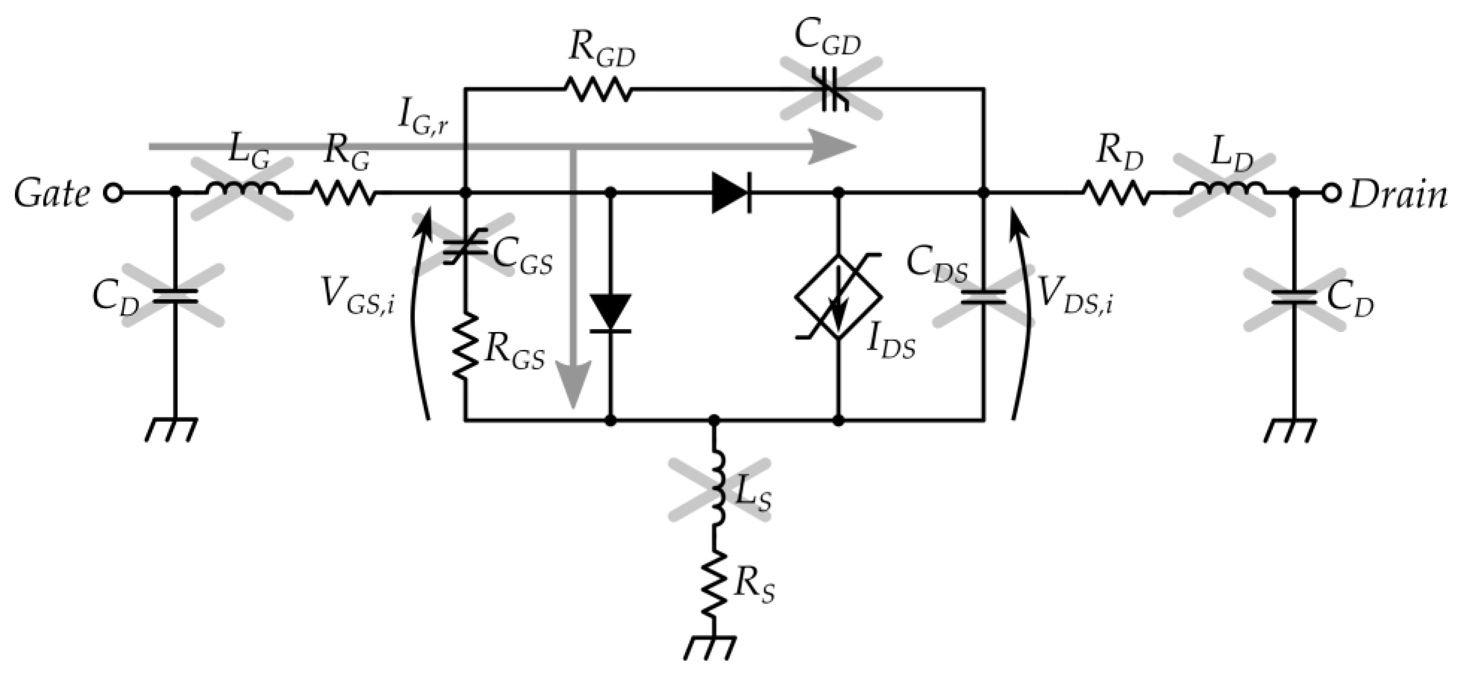
2. Characterization Technique

The proposed technique for evaluating the degradation effects on microwave transistors is based on the exploitation of low-frequency time-domain load-pull measurements. The term “low frequency” as defined herein refers to an operating frequency in the megahertz range, at which the microwave device behaves approximately as a “resistive” component, since the reactive effects associated with the parasitic elements and the intrinsic nonlinear capacitances produce negligible effects (Figure 1) [33]. This enables the access to electrical quantities that cannot be directly monitored under a microwave regime, such as the resistive gate current, i.e., the current flowing through the gate Schottky junction in a HEMT when excited under forward and/or reverse conduction. This quantity is usually hidden at microwave frequencies due to contributions of the reactive currents, which are orders of magnitude higher, leaving the average gate current as the only indicator related to the Schottky junction conduction regime. Nevertheless, this might lead to misleading information. As an illustrative example, Figure 2 shows two different gate current waveforms having the same average value but representing very different conditions. The blue waveform shows only the forward conduction of the Schottky junction (i.e., the positive current), whereas the red one also exhibits the reverse conduction, with a consequent increase of the forward current to keep the average value constant. Clearly, the latter is a more critical condition for the device, but it is impossible to infer only based on the average current.
Operating at a low frequency also enables the direct access to the so-called current-generator plane of the transistor, i.e., the intrinsic active part of the device. Power amplifier design techniques are generally related to this reference plane, defining the waveforms and/or the load terminations that the transistor current generator must experience to implement a specific class of operation [34,35]. The direct access to this plane enables the possibility of accurately controlling and monitoring the operating condition of the device by properly setting the input signals and the load conditions.
The choice of an operating frequency in the megahertz range for the characterization of microwave devices also allows one to account for the so-called low-frequency dispersion phenomena, i.e., the effects of thermal and trapping phenomena, which influence the electrical characteristics of the transistor [36,37,38,39,40]. Thermal effects depend on the junction temperature, i.e., the temperature that the device channel reaches during operation because of the power dissipation. Trapping phenomena are related to the presence of electron traps into the layers of material composing the transistor and consisting of energy levels that the carriers can occupy, being subtracted from conduction. These phenomena depend on the electric fields applied to the device, which are strictly related to the operating condition, especially in GaN devices where fast-trapping is an unavoidable issue connected to the maximum field instantaneously applied to the transistor [41]. Thermal and trapping effects are intrinsically intertwined [39,42,43] and are characterized by time constants relatively low when compared to the timing of a microwave signal [33,36,39,40], as well as that of the low-frequency characterization. Therefore, the data gathered from the low-frequency measurements are consistent with the microwave behavior of the device, being the cut-off frequency of these effects below a few megahertz.
The schematic of the setup that implements the measurement technique is reported in Figure 3. The device under test (DUT) is biased by a DC source measure unit (SMU, HP 4155B) with a high resolution (4 µV; 20 fA) and accuracy (V: 0.05%, I: 0.2%). On the input side, a commercial bias tee is used (Minicircuit ZX85-12G-S+, frequency range: 200 kHz–12 GHz), whereas on the output side a dedicated bias tee has been designed to support high-power levels (frequency range: 200 kHz–200 MHz, maximum voltage: 100 V, maximum current: 2 A, and power handling: 30 W). They provide DC-to-AC isolation and prevent low-frequency instabilities. Incident and reflected waves at the DUT ports are separated by two dual-directional couplers (frequency range: 10 kHz–400 MHz) and sent to a 12-bit 350-MHz 4-channel oscilloscope (Tektronix MSO54) for the acquisition. The input signal is provided by an arbitrary function generator (Tektronix AFG 3252). Regarding the load condition, it is important to stress that, by operating at a few megahertz, we can directly control the current-generator load. Therefore, once the class of operation to be investigated is defined, we can know and synthesize the corresponding load condition at the fundamental and harmonic frequencies. To this purpose, we designed and produced an electronically controllable tuner coupled with a frequency multiplexer, which controls the load impedance up to the third harmonic, allowing the synthesis of both conventional and high-efficiency classes of operation that require a harmonic manipulation of the load (e.g., class-F conditions). In case this is not sufficient, we can easily design a customized board that also implements the terminations required for the characterization at higher harmonics (if required) which can also be dimensioned to sustain high power levels, thus enabling the possibility of characterizing devices with very large peripheries.
The setup is fully controlled by an internally developed software, that includes the possibility of implementing a stress-measurement routine to evaluate the degradation effects of the specific operating condition applied to the DUT. In this context, an important role is played by the calibration, which must be stable over time. This is easily achieved at megahertz frequencies, where the time-varying characteristics of instruments and components have negligible effects and provide a stable system for long periods of time.

3. Implementation and Definition of the Stress Measurement

The software controlling the measurement setup allows the user to organize a set of automatic measurements that will be carried out sequentially on the DUT. The user can choose between stress measurements and control measurements. In the first case, a defined operating condition is applied to the DUT for a certain period of time, during which the main electrical quantities of interest are periodically monitored and sampled. The control measurements, instead, are thought to be carried out in between stress sessions to check the status of the DUT under operating conditions different from the one selected for the stress. Stress measurements can be chosen among:
  • DC stress: a bias point is applied to the DUT for a time T s t r e s s , during which the DC currents and voltages are periodically measured with a sampling time T s , D C . In this case, no signal is applied to the DUT.
  • Low-frequency stress: a large-signal operating condition at a low frequency is applied to the DUT for a time T s t r e s s , during which both average currents and voltages as well as the incident and reflected waveforms are periodically measured. The sampling time for the DC quantities ( T s , D C ) and for the waveforms ( T s , A C ) can be different.
The available control measurements are:
  • DC measurements: DC I/V characteristics are measured over a grid of bias points defined by the user.
  • Low-frequency measurements: a large-signal low-frequency characterization is carried out on the DUT. The investigated condition can be different with respect to the one used for the stress measurement and the user can choose among a single load line, a power sweep, a load sweep or both.
Although the software provides great flexibility in the definition of the measurement sequence, the typical choice, which has been used also for the characterization presented in this paper, is schematically depicted in Figure 4. A preliminary set of control measurements is carried out on the DUT to obtain its initial state. Then, the total stress time is divided into several stress sessions followed by intermediate control measurements to evaluate the degradation of the DUT under different conditions and to monitor the evolution of its state. Eventually, a final set of control measurements is carried out to characterize the final state of the DUT.

4. Measurement Description

The aim of this experiment is to verify how different operating conditions act on the device degradation. Therefore, we selected two samples from the same 0.15 µm gallium nitride HEMT technology with 600 µm total periphery and characterized each of them with a different stress condition. A preliminary characterization of the technology, which is not reported here for the sake of brevity, has shown an extremely low level of process dispersion between samples, which was necessary to guarantee a fair comparison between the selected samples.
The investigated stress conditions were selected in order to emphasize two possible degradation mechanisms. The first one puts the device under thermal stress, by exploiting a large-signal condition with a high level of power dissipation. To this aim, we selected the tuned-load class-AB operation [35,44] under saturated output power. The second one, on the contrary, has a lower level of power dissipation but forces the device to sustain high electric fields. That is a class-E condition [45,46], which is characterized by a load line that reaches very high drain voltage values [47,48]. We want to point out that the effects of high temperature and electric fields can be (and usually are) investigated by DC measurements. Nevertheless, that condition is not realistic, whereas the low-frequency characterization provides data under nonlinear dynamic operation that could be directly related to the microwave performance of the device.
Each stress condition was initially applied to a fresh device for a total time of 60 h, keeping the backside temperature at 30 °C. The total stress time was divided into eight shorter sessions of different durations, with DC control measurements in between. Then, the same measurement was repeated on each sample with the same timings but whilst increasing the substrate temperature up to 100 °C.
We report a summary of the measurement sequence in Table 1, whereas the details of the two stress conditions applied to the devices are reported in Table 2. The latter are the results acquired at the very beginning of the measurement at 30 °C, corresponding to the waveforms reported in Figure 5. Figure 5c clearly represents one of the advantages of the low-frequency characterization, i.e., the acquisition of the resistive gate current waveform. In the class-AB condition under saturated power, the forward conduction of the gate junction is evident, with a maximum instantaneous value of about 9 mA/mm. Under class-E operation, there is no forward conduction, but the drain voltage reaches a maximum value that is 63% higher with respect to the class-AB operation.
The load lines synthesizing the two classes of operation, i.e., tuned-load class AB and class E, were not selected with the aim of designing best-in-class amplifiers, but in order to evidence the theoretical differences existing between the two classes. In particular, the investigated load lines enforced a nonlinear dynamic regime for the device, showing a different drain-gate voltage peak, and the conduction of the Schottky junction, as well as efficiency and output power level.
The variations in the RF performance, expected during a degradation experiment, could be partly related to some drift of the load condition during such a long-lasting characterization. To manage this issue, the adopted load terminations were carefully designed to minimize the impact of the operating condition (e.g., dissipated power) on their value. Also, external factors, such as the ambient temperature, were controlled to limit their influence on the circuits implementing the load. Indeed, the load condition, which can be monitored directly from the acquired data, demonstrated an excellent stability, and its variations were limited to less than 1 Ω for both the selected stress conditions at both the fundamental and harmonics.

5. Experimental Results

In the following six subsections, we will describe the achieved experimental results for each of the investigated stress conditions and compare them to analyze how they impact differently on the device degradation.

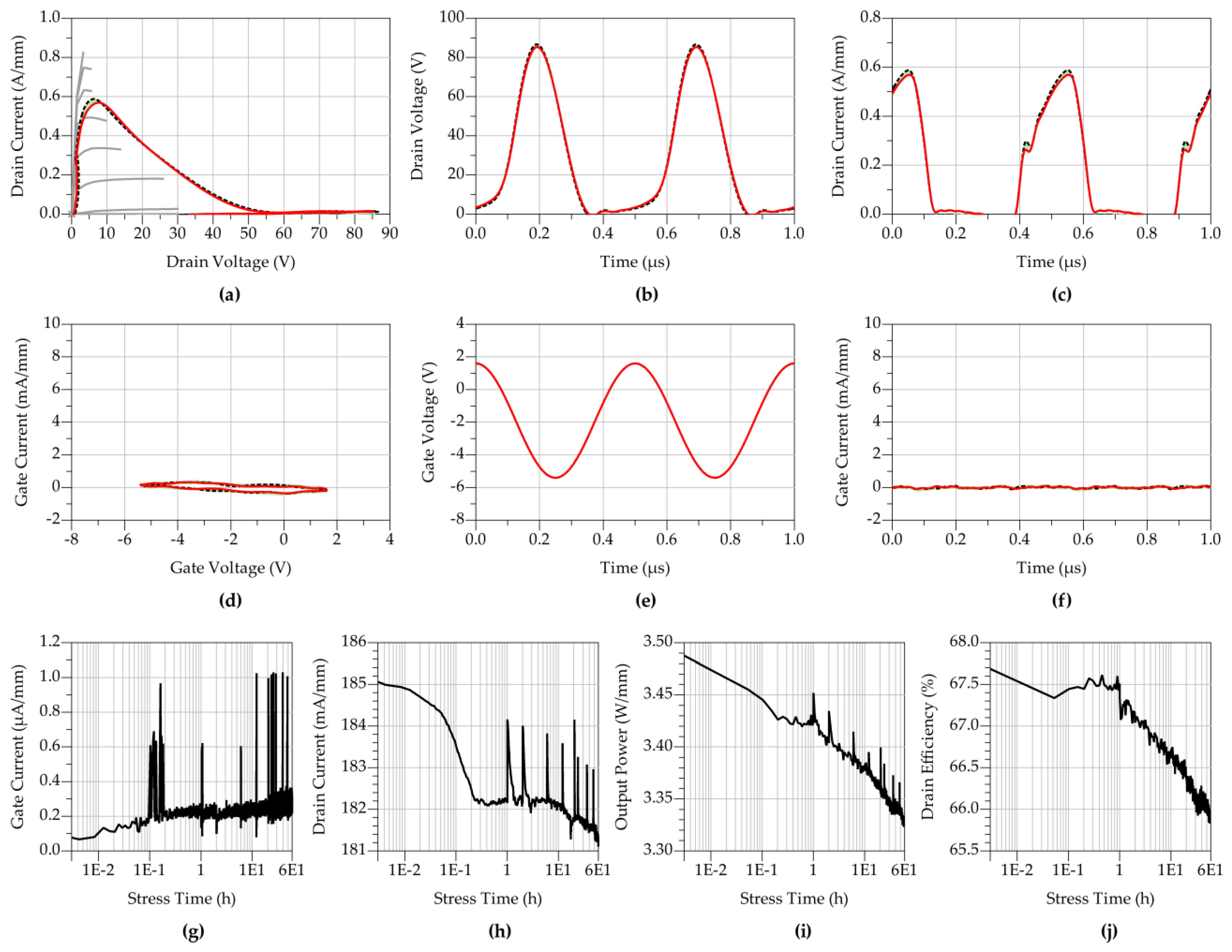
5.1. Tuned-Load Class-AB Stress at 30 °C

The stress condition has been applied to the DUT at 30 °C for a total of 60 h. We report the measured data in Figure 6, where both the waveforms and the performance are shown over the stress time. We can observe a slight variation in the load line (Figure 6a), mainly due to a reduction in the drain current, visible in Figure 6c. This translates into a decrease in the output power from 5.14 W/mm to 5.00 W/mm (–2.7%), and in the drain efficiency, from 65% to 64.4%, as shown in Figure 6i,j, respectively. Concerning the input side, no significant change was observed for the gate voltage waveform, whereas the peak of the gate current tended to decrease with the stress time from 9.3 mA/mm to 8.5 mA/mm (–8.6%), as depicted in Figure 6f, reducing the average gate current consequently from 634 µA/mm to 562 µA/mm (–11.4%, Figure 6g).
It is worth highlighting that the average currents, especially on the gate side, presented some sudden increases. This behavior was caused by the temporary suspension of the stress condition to perform the intermediate control measurements. During this time, the device experienced some recovery because of the change in the applied operating condition. Nevertheless, such a recovery was not permanent, since, as clearly shown in Figure 6g, after a brief transient, the data aligned to the previous data. This behavior was independent of the applied stress condition and, therefore, is present in all the results shown in the following.
In Figure 7, we report the data collected from the DC control measurements executed in between stress sessions. We note a mild reduction of the saturated drain current from 851 mA/mm to 833 mA/mm (−2.1%, Figure 7b) and a small variation of the threshold voltage, here represented in Figure 7c, where the gate voltage that provides a drain current of 100 mA/mm is reported as function of the stress time.

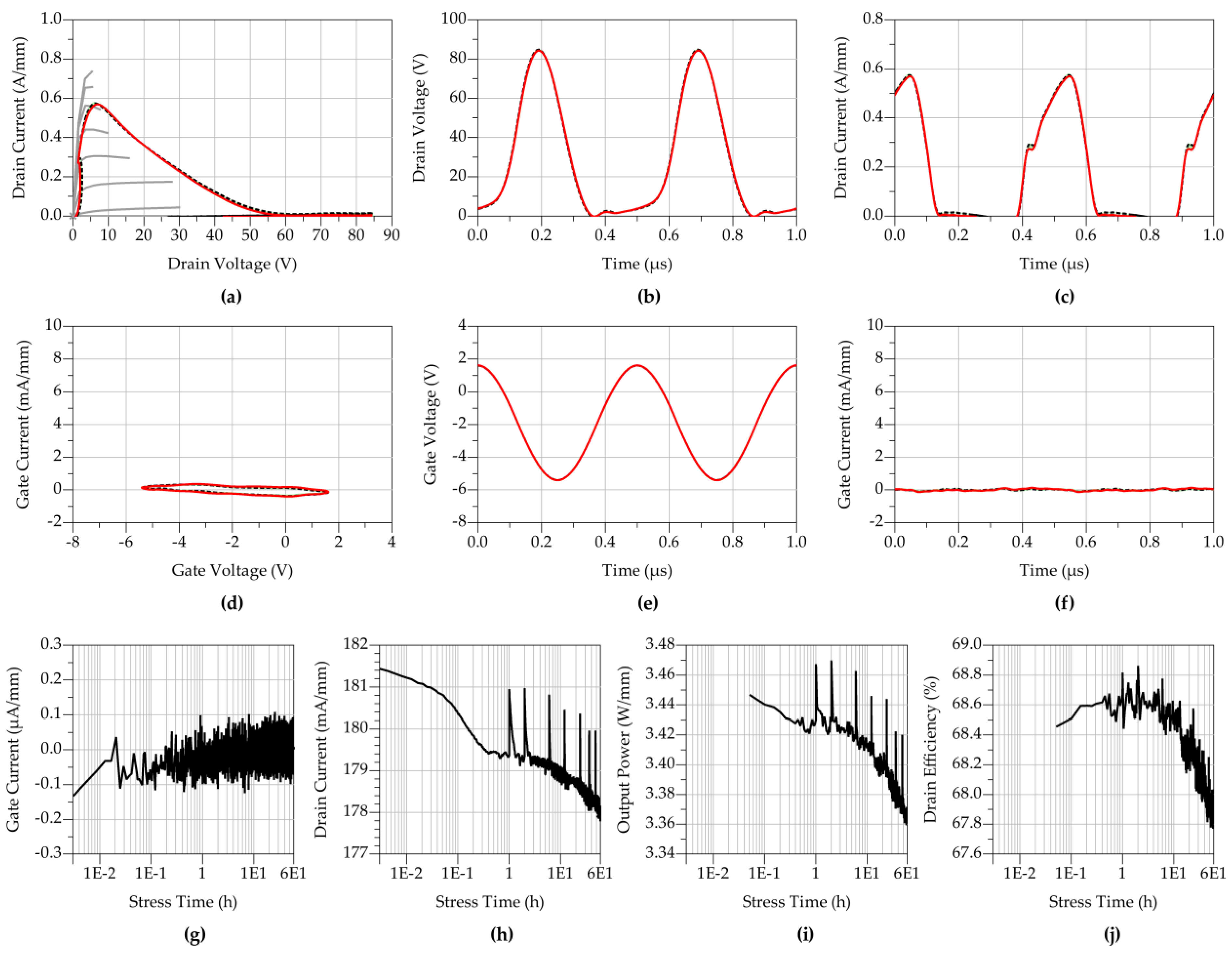
5.2. Class-E Stress at 30 °C

As in the previous case, the class-E stress condition was applied to a new sample at 30 °C for a total of 60 h. We report the waveforms and the performance evolution throughout the stress measurement in Figure 8. We can observe a slight variation of the load line (Figure 8a), this time due to a reduction in both the drain voltage and the drain current, whose peak value decreased from 86.7 V to 85.3 V (−1.6%), as illustrated in Figure 8b,c. This produces a reduction in the output power from 3.48 W/mm to 3.33 W/mm (−4.6%), and in the drain efficiency, from 67.7% to 66.0%, as shown in Figure 8i,j, respectively. In this case, the gate current was negligible throughout the entire experiment, since neither forward nor reverse conduction of the Schottky junction was present. Therefore, no significant change was observed in the input waveforms (Figure 8d–f). The evolution of the average currents over the stress time is also interesting. The average gate current was slightly positive but very small and became very noisy after approximately 0.1 h from the beginning of the measurement. The average drain current also exhibited a peculiar behavior. The largest variation appeared at the very beginning of the test, with a sharp decrease around 0.1 h. Then, it seemed to settle for 10 h, and to decrease again until the end of the measurement. It is interesting to observe that when the average drain current shows the faster variations, the average gate current becomes noisier, highlighting that the device behavior is changing due to some degradation mechanism.
In Figure 9, we show the data collected from the DC control measurements executed in between stress sessions. The results show a similar trend to the previous ones, although the decrease in the DC drain current (from 866 mA/mm to 820 mA/mm, −5.3%) and the change in the device threshold seem more accentuated.

5.3. Comparison of the Degradation Obtained at 30 °C

Some of the differences between the two investigated stress conditions have been already discussed. Nevertheless, we can now compare the level of degradation achieved by the devices after the stress tests.
Since the stress conditions are different, we will compare quantities normalized with respect to their initial values, also to compensate for some small process variations always present between samples, although very limited in our case. Therefore, the comparisons shown in Figure 10 are related to the relative percentage variation of various parameters, following the definition in Equation (1):
Δ X % = 100 X ( t ) X ( 0 ) X ( 0 )
where X ( t ) represents the generic quantity X after a time t from the beginning of the stress experiment ( t = 0 s).
From the data reported in Figure 10, the class-E operation produces a higher degradation of the device performance with respect to the class-AB condition in this first experiment. This suggests that the higher drain voltage reached by the class-E load line accelerates the degradation mechanisms. An interesting result confirming this phenomenon can be seen in the different trends of the average drain current (Figure 10b). For the class-E condition, the largest variation of the current appears within the first 20 min, whereas under class-AB the degradation appears more gradual throughout the stress.
Regarding the leakage gate current, one of the most important indicators of the device degradation, we observed a similar variation for both stress conditions. Here, the class-E condition seems less critical, although the measurements of this quantity were very noisy, and a conclusion based only on this parameter is not clear. This is highlighted also in Figure 11, where we compare the complete I-V characteristics measured before and after the stress measurement. By looking at the ID-VD characteristics, the global degradation seems negligible, thus suggesting that the effect of the applied stress is mainly related to the dynamic behavior of the transistors.

5.4. Tuned-Load Class-AB Stress at 100 °C

After the class-AB stress measurement at 30 °C was completed, it was repeated on the same device while raising the backside temperature to 100 °C. By doing this, we expected an acceleration in the degradation phenomena. The results of this characterization are reported in Figure 12 and Figure 13. It is immediately visible that the drain current was lower as compared to the previous cases, which is expected because of the reduction of the carrier mobility due to the higher temperature. During the stress, the load line showed a bigger variation, leading to a reduction in the output power and drain efficiency, respectively from 4.80 W/mm to 4.55 W/mm (−5%) and from 63.6% to 62.0%, as illustrated in Figure 12i,j.
Interesting results can be seen in the behavior of the gate port. First, the maximum value of the gate current waveform was significantly reduced with respect to the 30 °C case, which was, again, expected because of the higher temperature. The peak on the current reduced with stress time from 3.4 mA/mm to 2.3 mA/mm (−15%), although it seemed to settle after 10 h (Figure 12f), which is confirmed by the data related to the average gate current (Figure 12g). We also note that, during the stress, the shape of the current waveform changed, and a small current appeared when the Schottky junction operated below its threshold. As the gate current is a good indicator of the degradation of the transistor, this clearly confirms that the state of the device changed. We also point out that this kind of variation would be unknown if the measurements were carried out at microwaves frequencies.
The data concerning the DC control measurements are presented in Figure 13. Again, we observed a reduction in the saturated drain current from 720 mA/mm to 690 mA/m (−4.2%, Figure 13b), whereas the device threshold voltage changes during the stress but after 60 h settles on approximately the same value measured before the stress.

5.5. Class-E Stress at 100 °C

The same experiment at 100 °C was carried out on the second device sample, already stressed under class-E operation at 30 °C. The results are reported in Figure 14 and Figure 15. Looking at the waveforms reported in Figure 14, it is immediately evident that the status of the device changed less when compared to the previous measurement. The maximum drain voltage along the load line decreases from 84.7 V to 84.2 V (−0.6%). The output power goes from 3.45 W/mm before the stress to 3.36 W/mm after the stress (−0.3%), and, consequently, the drain efficiency reduces from 68.5% to 67.9%, as shown in Figure 14i,j, respectively.
No significant change was observed on the gate waveforms, where the gate current remained negligible throughout the entire experiment (Figure 14d–f). Looking at the small average gate current over the stress time (Figure 14g), we note very noisy data which became even noisier towards the end of the experiment, although on average they did not highlight any significant variation. The drain current instead has a behavior similar to the one observed at a lower temperature, with a sudden change around 0.1 h, a stable phase up to 5 h and then a more gradual decrease till the end of the experiment.
Figure 15 shows the results from the 100 °C DC control measurements, which have a similar trend with respect to the ones achieved at 30 °C, although the entity of the variations of the drain current (from 722 mA/mm to 705 mA/mm, −2.4%) and of the device threshold are more limited.

5.6. Comparison of the Degradation Obtained at 100 °C

Following the same approach adopted in Section 5.3, we will now compare the level of degradation obtained from the two operating conditions at 100 °C.
Looking at the results presented in Figure 16, in this case the class-AB operation is the one that provides a higher degradation of the device performance. All the reported parameters, including the gate leakage current, show how the performance of the class-E condition remains more stable and produces a lower alteration of the device behavior also under DC operation. This kind of result suggests that the thermal state of the device is the dominant factor in the degradation mechanisms and therefore, in this context, the class-AB operation is unfavorable compared to class-E condition, because of the higher power dissipation.
We report the complete I-V characteristics measured before and after the stress measurement in Figure 17. Again, these results confirm the previous observations, with the class-AB case showing the largest variation in the DC characteristics. In this case, the different levels of degradation achieved by the two conditions were clearly visible on the gate leakage current, which experienced the biggest variation (−62% vs. −32%) when the device operated under saturated class AB.

6. Conclusions

In this paper, we investigated how a realistic power amplifier operating condition can impact on the performance degradation of a GaN HEMT microwave devices. We compared the effects of a saturated class-AB condition and a high-efficiency class-E condition by means of stress experiments carried out using a low-frequency load-pull system. The thorough comparison of the experimental results clearly shows that:
  • The level of degradation reached by the device under test depends on the actual RF operating condition adopted for the stress experiment. This confirms the need for realistic stress tests to understand what specific degradation mechanisms can impact on the active device when used in actual applications and estimate its realistic lifetime.
  • Thermal degradation effects, magnified by the saturated class-AB condition, are more critical than the effects due to high fields, and dominant when the active device was operated under class-E condition.
  • The developed characterization methodology and the achieved experimental findings can be used to accurately and deeply investigate the degradation and failure mechanisms affecting microwave technology to enhance its performance and robustness for realistic operation in practical microwave applications.

Author Contributions

Conceptualization, G.B. and A.R.; methodology, G.B. and A.R.; software, G.B.; validation, G.B., A.R. and V.V.; formal analysis, G.B., A.R. and V.V.; investigation, G.B. and A.R.; resources, A.R. and R.G.; data curation, G.B.; writing—original draft preparation, G.B. and A.R.; writing—review and editing, V.V., R.G., G.C. and G.V.; supervision, A.R. and G.V.; project administration, A.R.; funding acquisition, A.R. and G.V. All authors have read and agreed to the published version of the manuscript.

Funding

This research was funded in part by the Italian Ministry of University and Research (MUR) through the PRIN 2017 Project under Grant 2017FL8C9N.

Data Availability Statement

Not applicable.

Conflicts of Interest

The authors declare no conflict of interest.

References

  1. Formicone, F.; Burger, J.; Custer, J.; Bosi, G.; Raffo, A.; Vannini, G. Solid-state RF power amplifiers for ISM CW applications based on 100 V GaN technology. In Proceedings of the 11th European Microwave Integrated Circuits Conference, London, UK, 3–4 October 2016. [Google Scholar]
  2. Pace, L.; Colangeli, S.; Ciccognani, W.; Longhi, P.E.; Limiti, E.; Leblanc, R.; Feudale, M.; Vitobello, F. Design and validation of 100 nm GaN-On-Si Ka-band LNA based on custom noise and small signal models. Electronics 2020, 9, 150. [Google Scholar] [CrossRef] [Green Version]
  3. Camarchia, V.; Quaglia, R.; Piacibello, A.; Nguyen, D.P.; Wang, H.; Pham, A.-V. A review of technologies and design techniques of millimeter-wave power amplifiers. IEEE Trans. Microw. Theory Tech. 2020, 68, 2957–2983. [Google Scholar] [CrossRef]
  4. Ramella, C.; Pirola, M.; Florian, C.; Colantonio, P. Space-Compliant Design of a Millimeter-Wave GaN-on-Si Stacked Power Amplifier Cell through Electro-Magnetic and Thermal Simulations. Electronics 2021, 10, 1784. [Google Scholar] [CrossRef]
  5. Ghisotti, S.; Pisa, S.; Colantonio, P. S-band hybrid power amplifier in GaN Technology with Input/Output Multi Harmonic Tuned Terminations. Electronics 2021, 10, 2318. [Google Scholar] [CrossRef]
  6. Nasri, A.; Estebsari, M.; Toofan, S.; Piacibello, A.; Pirola, M.; Camarchia, V.; Ramella, C. Broadband class-J GaN Doherty power amplifier. Electronics 2022, 11, 552. [Google Scholar] [CrossRef]
  7. Scappaviva, F.; Bosi, G.; Biondi, A.; D’Angelo, S.; Cariani, L.; Vadalà, V.; Raffo, A.; Resca, D.; Cipriani, E.; Vannini, G. Advances in Ku-Band GaN single chip front end for space SARs: From system specifications to technology selection. Electronics 2022, 11, 2998. [Google Scholar] [CrossRef]
  8. Zeng, F.; An, J.X.; Zhou, G.; Li, W.; Wang, H.; Duan, T.; Jiang, L.; Yu, H. A comprehensive review of recent progress on GaN high electron mobility transistors: Devices, fabrication and reliability. Electronics 2018, 7, 377. [Google Scholar] [CrossRef] [Green Version]
  9. Meneghini, M.; De Santi, C.; Abid, I.; Buffolo, M.; Cioni, M.; Khadar, R.A.; Nela, L.; Zagni, N.; Chini, A.; Medjdoub, F.; et al. GaN-based power devices: Physics, reliability, and perspectives. J. Appl. Phys. 2021, 130, 181101. [Google Scholar] [CrossRef]
  10. McGenn, W.; Benedikt, J.; Tasker, P.; Powell, J.; Uren, M. RF waveform investigation of VSWR sweeps on GaN HFETs. In Proceedings of the 6th European Microwave Integrated Circuit Conference, Manchester, UK, 10–12 October 2011. [Google Scholar]
  11. Meneghesso, G.; Verzellesi, G.; Danesin, F.; Rampazzo, F.; Zanon, F.; Tazzoli, A.; Meneghini, M.; Zanoni, E. Reliability of GaN high-electron-mobility transistors: State of the art and perspectives. IEEE Trans. Device Mater. Relib. 2008, 8, 332–343. [Google Scholar] [CrossRef]
  12. Joh, J.; Del Alamo, J.A. Critical voltage for electrical degradation of GaN high-electron mobility transistors. IEEE Electron Device Lett. 2008, 29, 287–289. [Google Scholar] [CrossRef]
  13. Pazirandeh, R.; Wurfl, J.; Trankle, G. Comparison of DC measurement methods to determine GaN HEMT reliability. In Proceedings of the Reliability of Compound Semiconductors Digest, Greensboro, NC, USA, 11 October 2009. [Google Scholar]
  14. Meneghini, M.; Rossetto, I.; Rizzato, V.; Stoffels, S.; Van Hove, M.; Posthuma, N.; Wu, T.-L.; Marcon, D.; Decoutere, S.; Meneghesso, G.; et al. Gate stability of GaN-Based HEMTs with P-Type gate. Electronics 2016, 5, 14. [Google Scholar] [CrossRef]
  15. Rodriguez, J.A.; Tsoi, T.; Graves, D.; Bayne, S.B. Evaluation of GaN HEMTs in H3TRB reliability testing. Electronics 2022, 11, 1532. [Google Scholar] [CrossRef]
  16. Menozzi, R. Hot electron effects and degradation of GaAs and InP HEMTs for microwave and millimetre-wave applications. Semicond. Sci. Technol. 1998, 13, 1053–1063. [Google Scholar] [CrossRef]
  17. Meneghini, M.; Stocco, A.; Silvestri, R.; Meneghesso, G.; Zanoni, E. Degradation of AlGaN/GaN high electron mobility transistors related to hot electrons. Appl. Phys. Lett. 2012, 100, 233508. [Google Scholar] [CrossRef]
  18. Ruzzarin, M.; Meneghini, M.; Rossetto, I.; Van Hove, M.; Stoffels, S.; Wu, T.-L.; Decoutere, S.; Meneghesso, G.; Zanoni, E. Evidence of hot-electron degradation in GaN-Based MIS-HEMTs submitted to high temperature constant source current stress. IEEE Electron Device Lett. 2016, 37, 1415–1417. [Google Scholar] [CrossRef]
  19. Tanaka, K.; Morita, T.; Ishida, M.; Hatsuda, T.; Ueda, T.; Yokoyama, K.; Ikoshi, A.; Hikita, M.; Toki, M.; Yanagihara, M.; et al. Reliability of hybrid-drain-embedded gate injection transistor. In Proceedings of the IEEE International Reliability Physics Symposium, Monterey, CA, USA, 2–6 April 2017. [Google Scholar]
  20. McGenn, W.; Choi, H.; Lees, J.; Uren, M.J.; Benedikt, J.; Tasker, P.J. Development of a RF waveform stress test procedure for GaN HFETs subjected to infinite VSWR sweeps. In Proceedings of the IEEE/MTT-S International Microwave Symposium Digest, Montreal, QC, Canada, 17–22 June 2012. [Google Scholar]
  21. Brazzini, T.; Casbon, M.A.; Sun, H.; Uren, M.J.; Lees, J.; Tasker, P.J.; Jung, H.; Blank, H.; Kuball, M. Study of hot electrons in AlGaN/GaN HEMTs under RF Class B and Class J operation using electroluminescence. Microelectron. Reliab. 2015, 55, 2493–2498. [Google Scholar] [CrossRef]
  22. Saugnon, D.; Tartarin, J.G.; Franc, B.; Maher, H.; Boone, F. Fully automated RF-thermal stress workbench with S-parameters tracking for GaN reliability analysis. In Proceedings of the 13th European Microwave Integrated Circuits Conference, Madrid, Spain, 23–25 September 2018. [Google Scholar]
  23. Moultif, N.; Latry, O.; Joubert, E.; Ndiaye, M.; Moreau, C.; Goupy, J.-F.; Carton, P. Reliability assessment of AlGaN/GaN HEMTs on the SiC substrate under the RF stress. IEEE Trans. Power Electron. 2021, 36, 7442–7450. [Google Scholar] [CrossRef]
  24. Joh, J.; Del Alamo, J.; Chowdhury, U.; Jimenez, J. Correlation between RF and DC reliability in GaN high electron mobility transistors. In Proceedings of the Reliability of Compound Semiconductors Workshop, Monterey, CA, USA, 12 October 2008. [Google Scholar]
  25. Chini, A.; Fantini, F.; Di Lecce, V.; Esposto, M.; Stocco, A.; Ronchi, N.; Zanon, F.; Meneghesso, G.; Zanoni, E. Correlation between DC and rf degradation due to deep levels in AlGaN/GaN HEMTs. In Proceedings of the International Electron Devices Meeting, Baltimore, MD, USA, 7–9 December 2009. [Google Scholar]
  26. Verspecht, J. Large-Signal Network Analysis. IEEE Microw. 2005, 6, 82–92. [Google Scholar] [CrossRef]
  27. Teppati, V.; Ferrero, A.; Pisani, U. Recent Advances in Real-Time Load-Pull Systems. IEEE Trans. Instrum. Meas. 2008, 57, 2640–2646. [Google Scholar] [CrossRef] [Green Version]
  28. Teppati, V.; Bolognesi, C.R. Evaluation and reduction of calibration residual uncertainty in load-pull measurements at millimeter-wave frequencies. IEEE Trans. Instrum. Meas. 2012, 61, 817–822. [Google Scholar] [CrossRef]
  29. Benedikt, J.; Gaddi, R.; Tasker, P.J.; Goss, M. High-power time-domain measurement system with active harmonic load-pull for high-efficiency base-station amplifier design. IEEE Trans. Microw. Theory Tech. 2000, 48, 2617–2624. [Google Scholar] [CrossRef]
  30. Rumiantsev, A.; Ridler, N. VNA Calibration. IEEE Microw. 2008, 9, 86–99. [Google Scholar] [CrossRef]
  31. Raffo, A.; Di Falco, S.; Vadalà, V.; Vannini, G. Characterization of GaN HEMT low-frequency dispersion through a multiharmonic measurement system. IEEE Trans. Microw. Theory Tech. 2010, 58, 2490–2496. [Google Scholar] [CrossRef]
  32. Vadalà, V.; Raffo, A.; Di Falco, S.; Bosi, G.; Nalli, A.; Vannini, G. A load–pull characterization technique accounting for harmonic tuning. IEEE Trans. Microw. Theory Tech. 2013, 61, 2695–2704. [Google Scholar] [CrossRef]
  33. Raffo, A.; Bosi, G.; Vadalà, V.; Vannini, G. Behavioral modeling of GaN FETs: A load-line approach. IEEE Trans. Microw. Theory Tech. 2014, 62, 73–82. [Google Scholar] [CrossRef]
  34. Cripps, S.C. RF Power Amplifiers for Wireless Communications; Artech House: Boston, MA, USA, 2006. [Google Scholar]
  35. Colantonio, P.; Giannini, F.; Limiti, E. High Efficiency RF and Microwave Solid State Power Amplifiers; J. Wiley: Chichester, UK, 2009. [Google Scholar]
  36. Nalli, A.; Raffo, A.; Avolio, G.; Vadalà, V.; Bosi, G.; Schreurs, D.M.M.-P.; Vannini, G. Extremely low-frequency measurements using an active bias tee. In Proceedings of the 2013 IEEE MTT-S International Microwave Symposium, Seattle, WA, USA, 2–7 June 2013. [Google Scholar]
  37. Raffo, A.; Avolio, G.; Vadalà, V.; Bosi, G.; Vannini, G.; Schreurs, D. Assessing GaN FET performance degradation in power amplifiers for pulsed radar systems. IEEE Microw. Wirel. Comp. Lett. 2018, 28, 1035–1037. [Google Scholar] [CrossRef]
  38. Gryglewski, D.; Wojtasiak, W.; Kamińska, E.; Piotrowska, A. Characterization of self-heating process in GaN-based HEMTs. Electronics 2020, 9, 1305. [Google Scholar] [CrossRef]
  39. Angelotti, A.M.; Gibiino, G.P.; Florian, C.; Santarelli, A. Trapping dynamics in GaN HEMTs for millimeter-wave applications: Measurement-based characterization and technology comparison. Electronics 2021, 10, 137. [Google Scholar] [CrossRef]
  40. Raja, P.V.; Subramani, N.K.; Gaillard, F.; Bouslama, M.; Sommet, R.; Nallatamby, J.-C. Identification of buffer and surface traps in Fe-doped AlGaN/GaN HEMTs using Y21 frequency dispersion properties. Electronics 2021, 10, 3096. [Google Scholar] [CrossRef]
  41. Wang, W.; Liang, Y.; Zhang, M.; Lin, F.; Wen, F.; Wang, H. Mechanism analysis of dynamic on-state resistance degradation for a commercial GaN HEMT using double pulse test. Electronics 2021, 10, 1202. [Google Scholar] [CrossRef]
  42. Cioni, M.; Zagni, N.; Selmi, L.; Meneghesso, G.; Meneghini, M.; Zanoni, E.; Chini, A. Electric field and self-heating effects on the emission time of iron traps in GaN HEMTs. IEEE Trans. Electron Devices 2021, 68, 3325–3332. [Google Scholar] [CrossRef]
  43. Modolo, N.; De Santi, C.; Baratella, G.; Bettini, A.; Borga, M.; Posthuma, N.; Bakeroot, B.; You, S.; Decoutere, S.; Bevilacqua, A.; et al. Compact modeling of nonideal trapping/detrapping processes in GaN power devices. IEEE Trans. Electron Devices 2022, 69, 4432–4437. [Google Scholar] [CrossRef]
  44. Raffo, A.; Colantonio, P.; Cipriani, E.; Vadalà, V.; Bosi, G.; Martin-Guerrero, T.M.; Vannini, G.; Giannini, F. Theoretical consideration on harmonic manipulated amplifiers based on experimental data. In Proceedings of the Integrated Nonlinear Microwave and Millimetre-Wave Circuits Workshop, Taormina, Italy, 1–2 October 2015. [Google Scholar]
  45. Musio, A.; Vadalà, V.; Scappaviva, F.; Raffo, A.; Di Falco, S.; Vannini, G. A new approach to Class-E power amplifier design. In Proceedings of the 2011 Workshop on Integrated Nonlinear Microwave and Millimetre-Wave Circuits, Vienna, Austria, 18–19 April 2011. [Google Scholar]
  46. Camarchia, V.; Cipriani, E.; Colantonio, P.; Pirola, M.; Quaglia, R.; Cabria, L.; Ayllon, N. Characterization of a high power GaN device for class E PA design with non-sinusoidal stimulus. In Proceedings of the 11th European Microwave Integrated Circuits Conference, London, UK, 3–4 October 2016. [Google Scholar]
  47. Mediano, A.; Sokal, N.O. A Class-E RF power amplifier with a flat-top transistor-voltage waveform. IEEE Trans. Power Electron. 2013, 28, 5215–5221. [Google Scholar] [CrossRef]
  48. Mikolajewski, M. An off-nominal class E amplifier—Design oriented analysis. Electronics 2023, 12, 2203. [Google Scholar] [CrossRef]
Figure 1. Equivalent-circuit model of a microwave field-effect transistor operating at a low frequency.
Electronics 12 02939 g001
Figure 2. Examples of gate current waveforms having the same average value but representing very different conditions: forward and reverse conduction (red line), and only forward conduction (blue line).
Electronics 12 02939 g002
Figure 3. Block diagram of the low-frequency time-domain load-pull setup used for the characterization of microwave devices.
Electronics 12 02939 g003
Figure 4. Typical sequence for a stress experiment.
Electronics 12 02939 g004
Figure 5. Investigated stress conditions described in Table 1, i.e., tuned-load class AB (red continuous lines) and class E (blue dashed lines): (a) load lines, (b) gate voltage waveforms, (c) gate current waveforms, (d) drain voltage waveforms, and (e) drain current waveforms.
Electronics 12 02939 g005
Figure 6. Stress measurement results for the 2 MHz tuned-load class-AB condition at 30 °C: (a) load lines vs. initial DC I/V characteristics (grey lines), (b) drain voltage waveforms, (c) drain current waveforms, (d) input loci, (e) gate voltage waveforms, (f) gate current waveforms with the evolution of its maximum instantaneous value in the inset, (g) average gate current, (h) average drain current, (i) output power, and (j) drain efficiency. From (af), the black dashed lines represent the initial state of the DUT, whereas the red continuous lines represent the final state of the DUT.
Electronics 12 02939 g006
Figure 7. DC control measurements for the 2 MHz tuned-load class-AB condition at 30 °C: (a) ID-VG trans-characteristic measured before (black dashed line) and after (red continuous line) the stress, (b) saturated drain current at VG = 2 V versus stress time, and (c) gate voltage for ID = 100 mA/mm versus stress time.
Electronics 12 02939 g007
Figure 8. Stress measurement results for the 2 MHz class-E condition at 30 °C: (a) load lines vs. initial DC I/V characteristics (grey lines), (b) drain voltage waveforms, (c) drain current waveforms, (d) input loci, (e) gate voltage waveforms, (f) gate current waveforms, (g) average gate current, (h) average drain current, (i) output power, (j) and drain efficiency. From (af), the black dashed lines represent the initial state of the DUT, whereas the red continuous lines represent the final state of the DUT.
Electronics 12 02939 g008
Figure 9. DC control measurements for the 2 MHz class-E condition at 30 °C: (a) ID-VG transcharacteristic measured before (black dashed line) and after (red continuous line) the stress, (b) saturated drain current at VG = 2 V versus stress time, and (c) gate voltage for ID = 100 mA/mm versus stress time.
Electronics 12 02939 g009
Figure 10. Comparison between the degradation achieved from the class-AB (red continuous lines) and the class-E (blue dashed lines) stress conditions. Variations, along 60 h of stress, of (a) output power, (b) average drain current, (c) drain efficiency, (d) threshold voltage at ID = 100 mA/mm, (e) saturated drain current at VG = 2 V and VD = 4 V, and (f) gate leakage current at VG = −4 V and VD = 30 V.
Electronics 12 02939 g010
Figure 11. Complete I-V characteristics measured before (black dashed lines) and after (red and blue continuous lines) the 60 h stress. Data collected for the (a,c) class-AB stress and (b,d) class-E stress.
Electronics 12 02939 g011
Figure 12. Stress measurement results for the 2 MHz tuned-load class-AB condition at 100 °C: (a) load lines vs. initial DC I/V characteristics (grey lines), (b) drain voltage waveforms, (c) drain current waveforms, (d) input loci, (e) gate voltage waveforms, (f) gate current waveforms with the evolution of its maximum instantaneous value in the inset, (g) average gate current, (h) average drain current, (i) output power, and (j) drain efficiency. From (af), the black dashed lines represent the initial state of the DUT, whereas the red continuous lines represent the final state of the DUT.
Electronics 12 02939 g012
Figure 13. DC control measurements for the 2 MHz tuned-load class-AB condition at 100 °C: (a) ID-VG trans-characteristic measured before (black dashed line) and after (red continuous line) the stress, (b) saturated drain current at VG = 2 V versus stress time, and (c) gate voltage for ID = 100 mA/mm versus stress time.
Electronics 12 02939 g013
Figure 14. Stress measurement results for the 2 MHz class-E condition at 100 °C: (a) load lines vs. initial DC I/V characteristics (grey lines), (b) drain voltage waveforms, (c) drain current waveforms, (d) input loci, (e) gate voltage waveforms, (f) gate current waveforms, (g) average gate current, (h) average drain current, (i) output power, and (j) drain efficiency. From (af), the black dashed lines represent the initial state of the DUT, whereas the red continuous lines represent the final state of the DUT.
Electronics 12 02939 g014
Figure 15. DC control measurements for the 2 MHz class-E condition at 100 °C: (a) ID-VG trans-characteristic measured before (black dashed line) and after (red continuous line) the stress, (b) saturated drain current at VG = 2 V versus stress time, and (c) gate voltage for ID = 100 mA/mm versus stress time.
Electronics 12 02939 g015
Figure 16. Comparison between the degradation achieved from the class-AB (red continuous lines) and the class-E (blue dashed lines) stress conditions. Variations, along 60 h of stress of (a) output power, (b) average drain current, (c) drain efficiency, (d) threshold voltage at ID = 100 mA/mm, (e) saturated drain current at VG = 2 V and VD = 4 V, and (f) gate leakage current at VG = −4 V and VD = 30 V.
Electronics 12 02939 g016
Figure 17. Complete I-V characteristics measured before (black dashed lines) and after (red and blue continuous lines) the 60 h stress. Data collected for the (a,c) class-AB stress and (b,d) class-E stress.
Electronics 12 02939 g017
Table 1. Summary of the stress measurement sequence.
PhaseDescriptionDetails
Preliminary/Final
Control Measurements
Full DC I/V CharacteristicsVG = −4–2 V, step 0.5 V, VD = 0–30 V, step 2 V
DC IGVD TranscharacteristicVG = −4 V, VD = 0–30 V, step 0.5 V
DC IDVG TranscharacteristicVG = −4–2 V, step 0.1 V, VD = 4 V
Stress SessionsLow-Frequency Tuned-Load Class AB60 h total stress time divided into 8 sessions
(1 h–1 h–4 h–6 h–12 h–12 h–12 h–12 h)
Low-Frequency Class-E
Intermediate
Control Measurements
DC IGVD TranscharacteristicVG = −4 V, VD = 0–30 V, step 0.5 V
DC IDVG TranscharacteristicVG = −4–2 V, step 0.1 V, VD = 4 V
Table 2. Stress conditions applied at 30 °C.
ParameterSymbolTuned-Load Class ABClass-E
Quiescent Gate VoltageVGQ−1.8 V−1.9 V
Quiescent Drain VoltageVDQ *28 V28 V
Quiescent Drain CurrentIDQ80 mA/mm60 mA/mm
Fundamental Frequencyf02 MHz2 MHz
LoadZL60.5 + j4.7 Ω ∙ mm @ f085.3 + 112 Ω ∙ mm @ f0
4.6 − j0.2 Ω ∙ mm @ 2f035.8 − 144 Ω ∙ mm @ 2f0
3.7 + j0.4 Ω ∙ mm @ 3f06.40 − j64.0 Ω ∙ mm @ 3f0
Average Gate CurrentIG00.63 mA/mm≈0 mA/mm
Average Drain CurrentID0285 mA/mm185 mA/mm
Input Power AvailablePav16.3 dBm14.9 dBm
Output PowerPout5.1 W/mm3.5 W/mm
Dissipated PowerPdiss2.7 W/mm1.4 W/mm
Drain EfficiencyηD65%67.8%
Maximum Drain VoltagevDmax53.2 V86.7 V
* Suggested by the foundry.
Disclaimer/Publisher’s Note: The statements, opinions and data contained in all publications are solely those of the individual author(s) and contributor(s) and not of MDPI and/or the editor(s). MDPI and/or the editor(s) disclaim responsibility for any injury to people or property resulting from any ideas, methods, instructions or products referred to in the content.

