Article

Design and Realization of a Compact High-Frequency Band-Pass Filter with Low Insertion Loss Based on a Combination of a Circular-Shaped Spiral Inductor, Spiral Capacitor and Interdigital Capacitor

Radio Frequency Integrated Centre (RFIC), Kwangwoon University, Kwangwoon-ro, Nowon-gu, Seoul 01897, Korea
*
Author to whom correspondence should be addressed.
Submission received: 31 July 2018 / Revised: 10 September 2018 / Accepted: 10 September 2018 / Published: 12 September 2018
(This article belongs to the Special Issue Selected Papers from IEEE ICKII 2018)

Abstract

:
In this study, the proposed bandpass filter (BPF) connects an interdigital and a spiral capacitor in series between the two symmetrical halves of a circular intertwined spiral inductor. For the mass production of devices and to achieve a higher accuracy and a better performance compared with other passive technologies, we used integrated passive device (IPD) technology. IPD has been widely used to realize compact BPFs and achieve the abovementioned. The center frequency of the proposed BPF is 1.96 GHz, and the return loss, insertion loss and transmission zero are 26.77 dB, 0.27 dB and 38.12 dB, respectively. The overall dimensions of BPFs manufactured using IPD technology are 984 × 800 μ m 2 , which is advantageous for miniaturization and integration.

Graphical Abstract

1. Introduction

With the rapid development of mobile phones in the last few decades, the demand for bandpass filters (BPFs) with high performance and integration has increased. The main function of a BPF in a transmitter is to limit the bandwidth of the output signal to the band of the BPF. This will prevent the transmitter from interfering with other parts. At the receiver, the BPF prevents unwanted frequency signals from passing through and can receive or decode signals in the selected frequency range. BPFs optimize the signal-to-noise ratio and sensitivity by preventing noise in the receiver. Therefore, the performance of RF transmission and reception in the wireless communication system needs to be increased by removing noise signals and unnecessary frequency harmonic components other than the desired frequency band. When considering mobile phones and their products, compact size is an important requirement [1,2,3]. Most handheld devices have particularly stringent miniaturization requirements to meet market expectations.
For this reason, mobile phones demand BPFs with high performance and integration, as well as a compact size and low weight. According to this trend, researchers had used low temperature co-fired ceramic (LTCC) technology, and it was reported in [4,5,6]. Liquid crystal polymer (LCP) substrates were reported in [7,8]. However, LTCC and LCP are not only higher in cost and bigger in size, but also capacitance densities are low and process tolerance immature compared to the integrated passive device (IPD) technology. IPD technology has been widely used to realize compact BPFs and achieve these demands. IPD technology has advantages that include mass production of devices, high accuracy and better performance compared with other passive technologies. With IPD technology, it is possible to integrate individual passive components into a microwave device or system. IPD technology can now be applied to applications that use the entire passive device and is already applied to the front-end module of mobile systems. Many functional blocks such as filters, baluns, diplexers, transformers, directional couplers and power dividers in mobile telecommunication systems can be created using IPD technology. To obtain a compact BPF and an inductor with a high Q-factor, Yook et al. realized a BPF with a suspended spiral inductor on the substrate of an anodized aluminum oxide, but its insertion loss and return loss performances needed to be improved [9]. Chia et al. used two coupled spiral inductors integrated on an Al2O3 substrate, but it suffered from a high insertion loss [10].
In this paper, we present a BPF based on a combination of a circular-shaped spiral inductor, an interdigital capacitor and a spiral capacitor. The overall dimensions of the BPF manufactured using IPD technology are 984 × 800 μ m 2 which is advantageous for the telecom industry where miniaturization and integration are required. The loss due to the parallel capacitor between the signal electrode and ground electrodes can be reduced using a GaAs substrate. For applications to mobile phones, the BPF has been designed with a center frequency of 2.0 GHz, an insertion loss of 0.27 dB and a return loss of 26.76 dB. In addition, the transmission zero of 5.22 GHz in the stopband region of the filter suppresses signals above 38 dB to generate a wide stopband response.

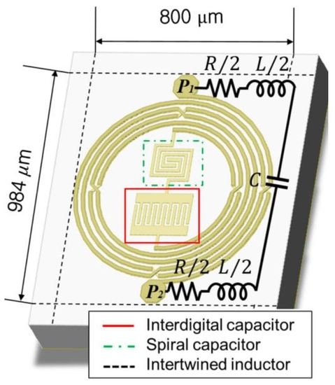
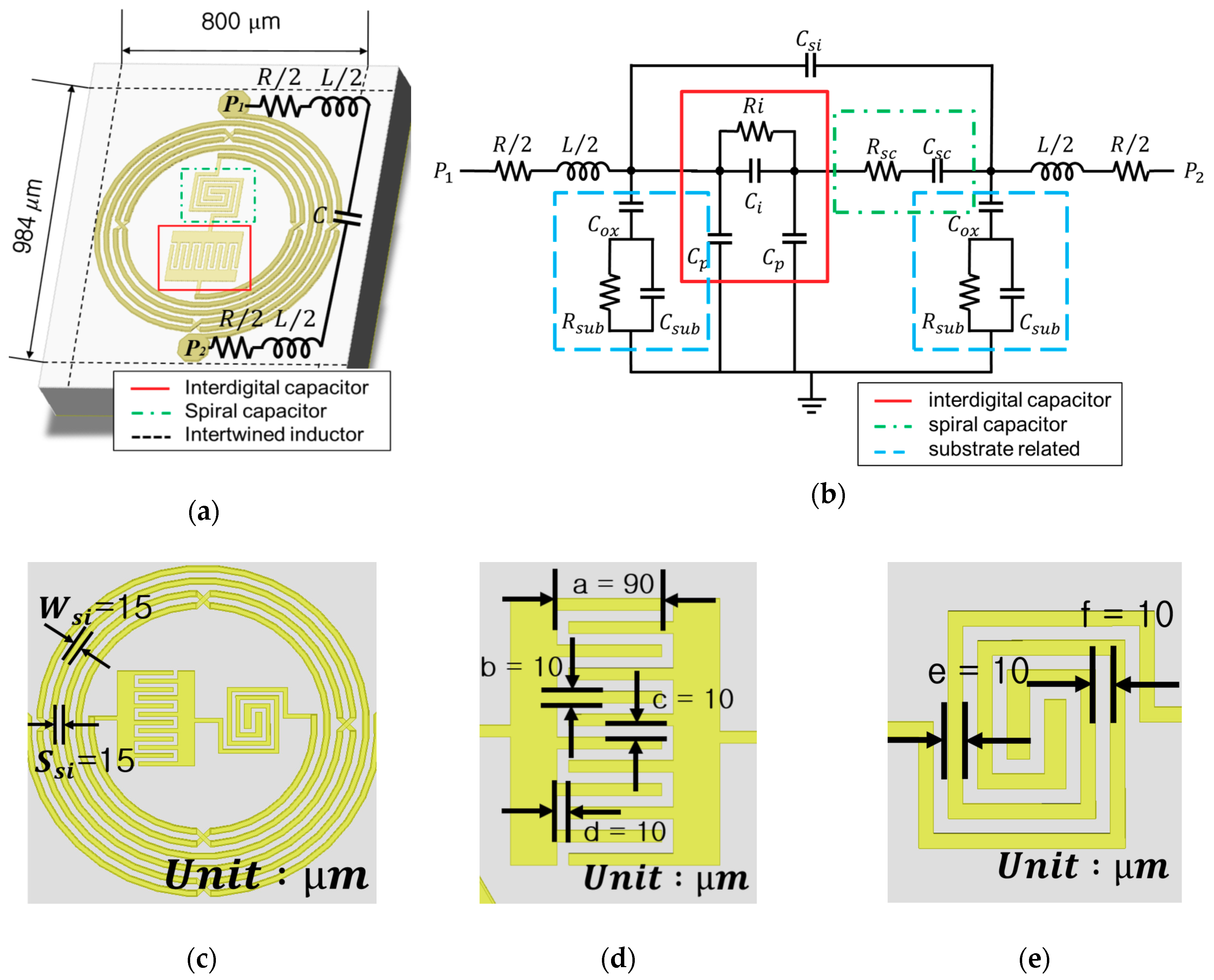
2. Materials and Methods

In order to improve the return loss and insertion loss performances, the proposed BPF is used on a GaAs substrate that can accept high speed microelectronics. High inductance can be achieved by fabricating two spiral inductors with SiNx between them. Thus, inductance can be improved by the mutual induction effect. Based on this technology, spiral and interdigital capacitors are connected in a circular intertwined spiral inductor to reduce return loss and insertion loss and to have a high Q-factor. By utilizing the internal space, it is possible to manufacture chips with a compact size. We designed the layout by using Agilent Advanced Design System (ADS) software (Version 2016. 01, Keysight Technologies, Inc., Santa Rosa, CA., USA) for the proposed BPF and simulated the results.
The proposed BPF connects the interdigital capacitor and spiral capacitor in series between the two symmetrical halves of a circular intertwined spiral inductor, as depicted in the schematic in Figure 1a. The substrate used for fabrication was a GaAs substrate with a diameter of 6 inch and a thickness of 200 μ m . The dielectric constant εr is 12.85, and the loss tangent is 0.006. A standard IPD manufacturing process is followed for filter fabrication [11].
Figure 1b shows the equivalent circuit of the proposed BPF. R denotes the resistance loss of the circular intertwined spiral inductor of inductance (L) with the substrate-related parameters COX, CSUB and RSUB. Csc and Rsc denote the coupling capacitance and loss resistance of the spiral capacitor [12,13]. Csi is the feedthrough capacitance. Ci and Ri represent the total capacitance and loss resistance of the interdigital capacitor. Cp represents the capacitance effect due to direct flux from the signal electrode to the ground electrode of the interdigital capacitor [14,15]. As shown in Figure 1c, the circular intertwined spiral inductor is deposited on the GaAs substrate and a 2000 Å-thick SiNx is placed between the two inductors. The inductance of a planar circular spiral inductor can be expressed as follows [16]:
L = μ 0 n 2 d a v g c 1 2 [ l n ( c 2 / ρ ) + c 3 ρ + c 4 ρ 2 ]
According to the expression based on the current sheet expression, c1, c2, c3 and c4 are layout-dependent coefficients, and their values are 1.00, 2.46, 0.00 and 0.20 for the circular inductor, respectively. The average diameter davg is 0.5 (dout + din), and dout and din denote the outer and inner diameters, respectively. N is the number of turns, and ρ is the fill ratio, which is expressed as ρ = (dout − din)/(dout + din).
In Figure 1d, the interdigital capacitors can be expressed as follows [17]:
C i = [ ε 0 ( 1 + ε s 2 )   K ( 1 + k 2 ) K ( k ) + ε 0 t a ] ( N 1 ) L
where ε 0 is the free space permittivity, ε s is the permittivity of the GaAs substrate and k = a/b and K (k) represent the first type of elliptic integral. N is the number of windings, and L is the length of the interdigital electrode.
Similarly, the spiral capacitor shown in Figure 1e can be expressed as follows [18]:
C s c = [ ε 0 ( 1 + ε s 2 )   K ( 1 + k 2 ) K ( k ) + ε 0 t a ] L c
where ε 0 and ε s denote the free space permittivity and permittivity of the GaAs substrate. The other part is Lc, and Lc is the total length of the spiral capacitor line.
The equivalent circuit of an intertwined spiral inductor, a spiral capacitor and an interdigital capacitor is shown in Figure 1b. The resonance frequency of the BPF is given as follows:
f 0 = 1 2 π L C
where L and C are the total inductance and capacitance of the proposed BPF, respectively.
Q = f 0 B 3 d B ,   B 3 d B = f H f L
The Q-factor determines the bandwidth of the resonator according to the center frequency. A high value of the Q-factor indicates that the energy loss is less than the energy stored in the resonator.

3. Results and Discussion
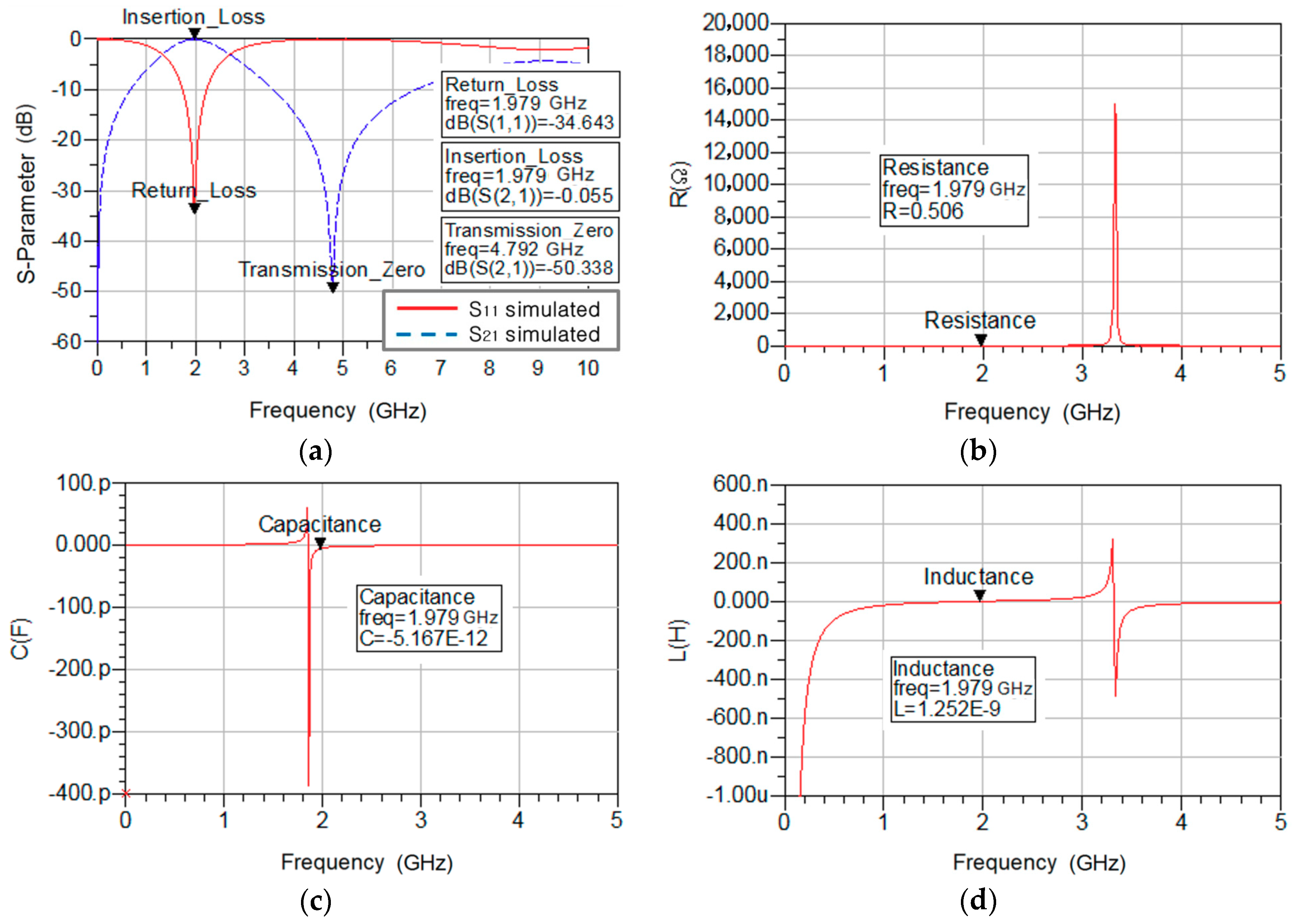
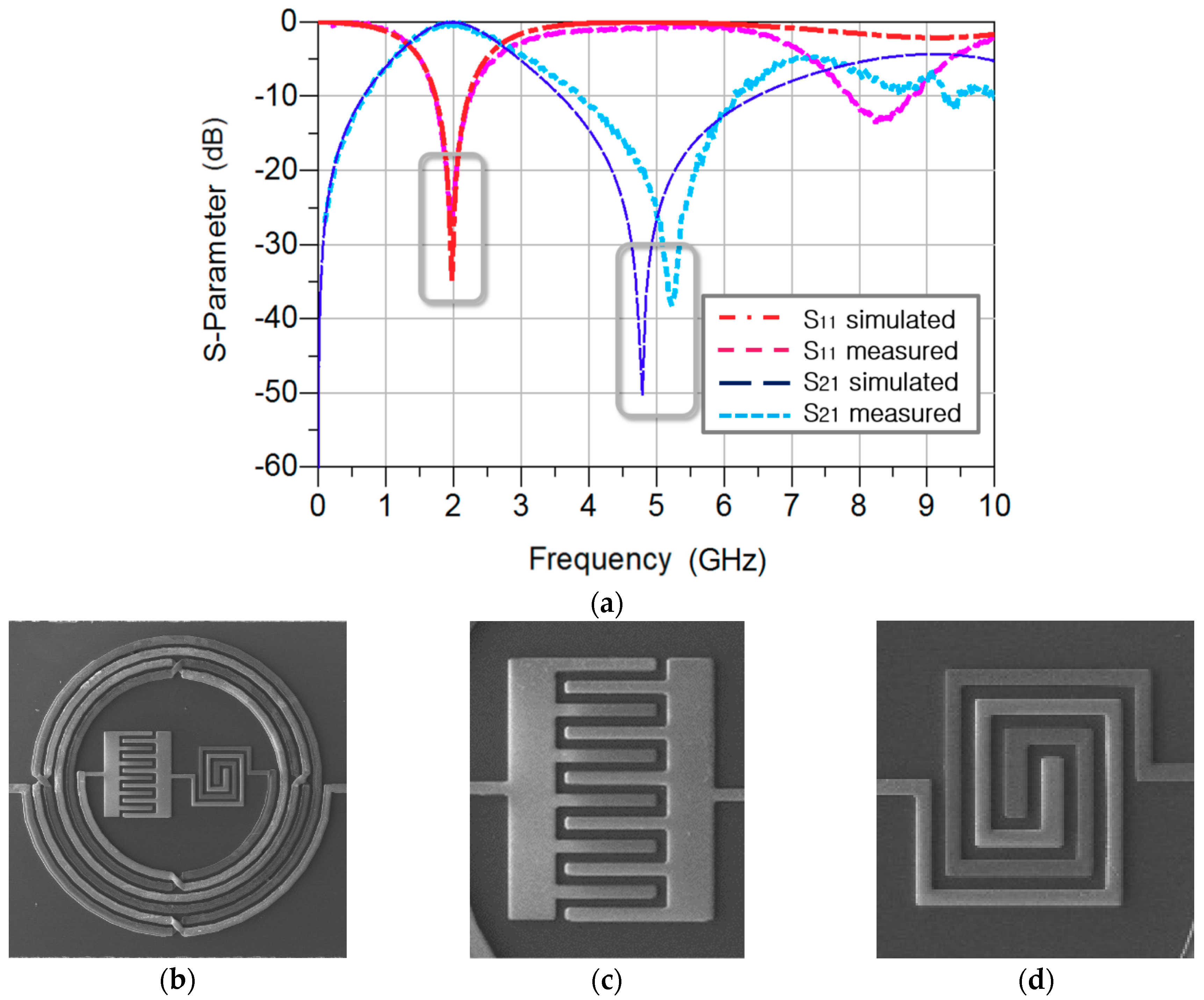
3.1. Results

The proposed BPF had a center frequency of 2 GHz and was simulated by ADS software to verify it. The center frequency of the BPF obtained from the simulation results was 1.98 GHz, and the return loss, insertion loss and Q-factor were 34.64 dB, 0.06 dB and 1.45, respectively. The optimized dimensions of the circular intertwined spiral inductor, spiral capacitor and interdigital capacitor are as follows.
  • • The circular intertwined spiral inductor is shown in Figure 1c:
  • : d i n = 530   μ m , d o u t = 800   μ m , L c = 1850   μ m , N = 5 , W s i = 15   μ m , S s i = 15   μ m
  • • Interdigital capacitor in Figure 1d:
  • : a = 90   μ m , b = 10   μ m , c = 10   μ m , d = 10   μ m ,
  • • Spiral capacitor in Figure 1e:
  • : e = 10   μ m , f = 10   μ m , n = 2
Figure 2 shows the simulation results of the BPF designed with the above parameters, and the frequency characteristics were confirmed by the S-parameter of the BPF. The frequency characteristics of the resistor, the capacitor and the inductor in Figure 1a are shown.
The Agilent 8510 vector network analyzer was used to identify the center frequency and characteristics of the fabricated BFP, as shown in Figure 3. The measured center frequency was 1.96 GHz, which was downshifted by approximately 20 MHz from the expected result of 1.98 GHz. The measured return loss, insertion loss and transmission zero were also changed. The measured return loss, insertion loss and transmission zero were 26.77 dB, 0.27 dB and 38.12 dB, respectively. The difference between the simulation results and measured results for the return loss, insertion loss and transmission zero was 7.87 dB, 0.21 dB and 12.22 dB, respectively, and there was a difference between the two results. For transmission zero, the frequency was upshifted to 431 MHz, and the Q-factor changed slightly from 1.45 to 1.41. The reason for the difference between simulation results and measurement results was caused by the dielectric loss of the substrate, the loss in the inductor bending and the accuracy of the physical dimensions. Because of that reason, resistance (from 0.51 Ω–1.74 Ω), capacitance (from 5.17 pF–6.37 pF) and inductance (from 1.25 nH–1.04 nH) also changed. Figure 3b–d displays the scanning electron microscopy (SEM) images of fabricated bandpass filters, interdigital capacitors and spiral capacitors, respectively.

3.2. Discussion

The main purpose of this study was to show that the performance and size of filters fabricated through the IPD process were unique and performed better when compared to other works. The proposed bandpass filter was a combined inductor and two capacitors including an intertwined spiral inductor, an interdigital capacitor and a spiral capacitor. By equivalent circuit, the series and parallel capacitor can be integrated into one capacitor. Because of this, the proposed filter can be analyzed by first-order inductor and capacitor (LC) BPF as the simulation and measurement result. The performance of the proposed filter was better than other works because the losses were reduced using a GaAs substrate. Especially, the insertion loss was greatly reduced. The manufactured filter using IPD technology made it difficult to know if the filter was fabricated well or not because of its small scale. Through SEM images, we can check that there is no problem in the process.
Table 1 indicates that the proposed BPF has a more compact size and a lower number of metal layers, which reduces the cost and fabrication complexity of the device. Further, the proposed BPF had a smaller insertion loss and a higher return loss compared with other reported BPFs. Table 1 shows a comparison of the parameters of the developed BPF with several recently reported IPD BPFs. IPD technology can realize the fabrication of small-sized BPF better than LTCC BPF [21]. Monolithic Microwave Integrated Circuit (MMIC) BPF is almost the same as IPD BPFs [10], but in order to have a high cut-off frequency, the overall size of the filter must be fabricated small. When considering the different center frequency IPD and MMIC technology, IPD BPFs can be realized as a small size and fabricated better than MMIC BPF. The BPF of this work had the lowest insertion loss, and the BPF could be easily and simply fabricated compared to other BPFs because we used only two metal layers.

4. Conclusions

In order to realize high performance BPFs along with miniaturization and integration required in the mobile industry, IPD technology was used in this study. IPD technology can achieve miniaturization and integration. When using the same substrate, it is possible to fabricate more BPFs that are miniaturized by IPD technology compared with BPFs manufactured by different processes on one substrate. This can lower the price of the BPF, which is advantageous for the mobile industry. To fabricate a BPF with good performance, the number of metal layers is increased. In this study, we used the space of the interdigital capacitor and spiral capacitor inside the circular intertwined spiral inductor by using only two metal layers. By using the GaAs substrate, it is possible to obtain a sharp band pass skirt selectivity with a small insertion loss and a large return loss. By reducing the number of metal layers, the structure is simplified, and the number of manufacturing steps can be reduced to lower the manufacturing cost. In the future, the mobile industry is expected to demand compact BPFs with a better performance. Thus, it is necessary to continue developing IPD technology to meet the future demands of the mobile industry.

Author Contributions

Conceptualization, K.-H.L.; Formal analysis, K.-H.L.; Investigation, E.-S.K.; Methodology, K.-H.L.; Resources, J.-G.L.; Supervision, N.-Y.K.; Writing—original draft, K.-H.L.; Writing—review & editing, J.-G.L. and N.-Y.K.

Funding

This research received no external funding.

Acknowledgments

This research was supported by the basic research project conducted with support from the Korea Research Foundation (NRF) and the government (Ministry of Education) in 2018 (No. 2018R1A6A1A03025242), as well as a 2018 research grant from Kwangwoon University.

Conflicts of Interest

The authors declare no conflict of interest.

References

  1. Yeung, L.K.; Wu, K.L. A Compact Second-Order LTCC Bandpass Filter With Two Finite Transmission Zeros. IEEE Trans. Microw. Theory Technol. 2003, 51, 337–341. [Google Scholar] [CrossRef]
  2. Zhang, S.; Rao, J.Y.; Hong, J.S.; Liu, F.L. A Novel Dual-Band Controllable Bandpass Filter Based on Fan-Shaped Substrate Integrated Waveguide. IEEE Microw. Wirel. Compon. Lett. 2018, 28, 308–310. [Google Scholar] [CrossRef]
  3. Xue, Q.; Jin, J.Y. Bandpass Filters Designed by Transmission Zero Resonator Pairs with Proximity Coupling. IEEE Trans. Microw. Theory Technol. 2017, 65, 4103–4110. [Google Scholar] [CrossRef]
  4. Wu, M.C.; Chung, S.J. A Small SiP Module Using LTCC 3D Circuitry for Dual Band WLAN 802.11a/b/g Front-End Solution. In Proceedings of the IEEE Topical Meeting on Silicon Monolithic Integrated Circuits in RF Systems, San Diego, CA, USA, 18–20 January 2006; pp. 174–177. [Google Scholar] [CrossRef]
  5. Ko, Y.J.; Park, J.Y.; Ryu, J.H.; Lee, K.H.; Bu, J.U. A Miniaturized LTCC Multi-layered Front-end Modulefor Dual Band WLAN (802.1 la/b/g) Applications. In Proceedings of the 2004 IEEE MTT-S International Microwave Symposium Digest, Fort Worth, TX, USA, 6–11 June 2004; pp. 563–566. [Google Scholar] [CrossRef]
  6. Kundu, A.; Mellen, N. Miniaturized Multilayer Bandpass Filter with Multiple Transmission Zeros. IEEE MTT-S Int. Microw. Symp. Dig. 2006, 760–763. [Google Scholar] [CrossRef]
  7. Swaminathan, M.; Bavisi, A.; Yun, W.; Sundaram, V.; Govind, V.; Monajemi, P. Design and Fabrication of Integrated RF Modules in Liquid Crystalline Polymer (LCP) Substrates. In Proceedings of the Conference of IEEE Industrial Electronics Society, Raleigh, NC, USA, 6–10 November 2005; pp. 2346–2351. [Google Scholar] [CrossRef]
  8. Sarkar, S.; Palazarri, V.; Wang, G.; Papageorgiou, N.; Thompson, D.; Lee, J.H.; Pinel, S.; Tentzeris, M.M.; Papapolymerou, J.; Laskar, J. RF and mm-wave SOP Module Platform using LCP and RF MEMS Technologies. In Proceedings of the Conference IEEE MTT-S International Microwave Symposium Digest, Fort Worth, TX, USA, 6–11 November 2004; pp. 567–570. [Google Scholar] [CrossRef]
  9. Yook, J.M.; Kim, K.M.; Kwon, Y.S. Suspended Spiral Inductor and Band-Pass Filter on Thick Anodized Aluminum Oxide. IEEE Microw. Wirel. Compon. Lett. 2009, 19, 620–622. [Google Scholar] [CrossRef]
  10. Chia, S.W.; Chiu, H.C.; Lin, Y.F. Microwave band-pass filter and passive devices using copper metal process on Al2O3 substrate. Microw. J. 2008, 19, 620–622. [Google Scholar]
  11. Wang, C.; Lee, W.S.; Zhang, F.; Kim, N.Y. A novel method for the fabrication of integrated passive devices on SI-GaAs substrate. Int. J. Adv. Manuf. Technol. 2011, 52, 1011–1018. [Google Scholar] [CrossRef]
  12. Kim, E.S.; Kim, N.Y. Micro-Fabricated Resonator Based on Inscribing a Meandered-Line Coupling Capacitor in an Air-Bridged Circular Spiral Inductor. Micromachines 2018, 9, 294. [Google Scholar] [CrossRef]
  13. Li, Y.; Wang, C.; Kim, N.Y. A high performance compact Wilkinson power divider using GaAs-based optimized integrated passive device fabrication process for LTE application. Solid-State Electron. 2014, 103, 147–153. [Google Scholar] [CrossRef]
  14. Chuluunbaatar, Z.; Adhikari, K.K.; Wang, C.; Kim, N.Y. Micro-fabricated bandpass filter using intertwined spiral inductor and interdigital capacitor. Electron. Lett. 2014, 50, 1296–1297. [Google Scholar] [CrossRef]
  15. Li, Y.; Wang, C.; Kim, N.Y. Design of Very Compact Bandpass Filters Based on Differential Transformers. IEEE Micrw. Wirel. Compon. Lett. 2015, 25, 439–441. [Google Scholar] [CrossRef]
  16. Mohan, S.S.; Hershenson, M.D.M.; Boyd, S.P.; Lee, T.H. Simple Accurate Expressions for Planar Spiral Inductances. IEEE J Solid State Circuits 1999, 34, 1419–1422. [Google Scholar] [CrossRef]
  17. Bryan, H.E. Printed inductors and capacitors. Tele-Tech Electron. Ind. 1955, 14, 68. [Google Scholar]
  18. Ong, K.G.; Grimes, C.A. A resonant printed-circuit sensor for remote query monitoring of environmental parameters. Smart Mater. Struct. 2000, 9, 421–428. [Google Scholar] [CrossRef]
  19. Liu, K.; Frye, R.; Emigh, R. Band-Pass-Filter with Balun Function from IPD Technology. In Proceedings of the IEEE Electronic Components and Technology Conference, Lake Buena Vista, FL, USA, 27–30 May 2008; pp. 718–723. [Google Scholar] [CrossRef]
  20. Li, N.; Li, X.Z.; Xing, M.J.; Chen, Q.; Yang, X.D. Design of Super Compact Bandpass Filter Using Silicon-Based Integrated Passive Device Technology. In Proceedings of the IEEE International Conference on Electronic Packaging Technology (ICEPT), Harbin, China, 16–19 August 2017; pp. 1069–1072. [Google Scholar] [CrossRef]
  21. Zhang, X.Y.; Dai, X.; Kao, H.L.; Wei, B.H.; Cai, Z.Y.; Xue, Q. Compact LTCC Bandpass Filter With Wide Stopband Using Discriminating Coupling. IEEE Trans. Microw. Theory Technol. 2014, 4, 656–663. [Google Scholar] [CrossRef]
Figure 1. Proposed bandpass filter (BPF) based on integrated passive device (IPD) technology combined circular intertwined spiral inductor, interdigital capacitor and spiral capacitor: (a) the layout of the proposed BPF; (b) the equivalent circuit of the proposed BPF; (c) the layout of the proposed BPF; (d) enlarged layout of the interdigital capacitor; (e) enlarged layout of the spiral capacitor.
Electronics 07 00195 g001
Figure 2. Proposed BPF simulation result to get: (a) the S-parameter; (b) resistance; (c) capacitance; and (d) inductance.
Electronics 07 00195 g002
Figure 3. Proposed BPF: (a) comparison of simulated and measured results of BPF; (b) the scanning electron microscopy (SEM) image of the proposed BPF; (c) enlarged SEM image of the interdigital capacitor; (d) enlarged SEM image of the spiral capacitor.
Electronics 07 00195 g003
Table 1. Parameter comparison between proposed BPF and reported BPFs. LTCC, low temperature co-fired ceramic.
Ref.TechnologyCutoff Frequency (GHz)Insertion Loss (dB)Return Loss (dB)Size (mm2)Metal Layers
[19]Silicon IPD2.452.2301.5 × 1.53
[20]Silicon IPD1.72.0251.0 × 0.53
[21]LTCC2.42.4152.6 × 2.64
[9]Aluminum IPD2.452.8142.2 × 1.84
[10]Al2O3 MMIC5.22.529.10.81 × 0.683
[12]GaAs IPD1.630.424.20.88 × 1.02
[14]GaAs IPD2.270.826.10.9 × 0.72
This workGaAs IPD1.960.2726.80.8 × 9.82

